Introduction
Printed circuit boards (PCBs) are essential components in nearly all modern electronic devices. As such, PCB design software is a critical tool for electrical engineers and hardware developers. Two of the most popular PCB design programs are Solidworks PCB and Altium Designer. But what exactly sets these two platforms apart?
In this in-depth comparison guide, we’ll examine the key differences between Solidworks PCB and Altium when it comes to features, interface, pricing, and more. Whether you’re looking to choose between the two for a new project or simply want to learn about their respective capabilities, read on for a detailed look at how these rival PCB design solutions stack up.
Overview of Solidworks PCB and Altium Designer

Before diving into a feature-by-feature comparison, let’s briefly introduce both Solidworks PCB and Altium Designer.
Solidworks PCB
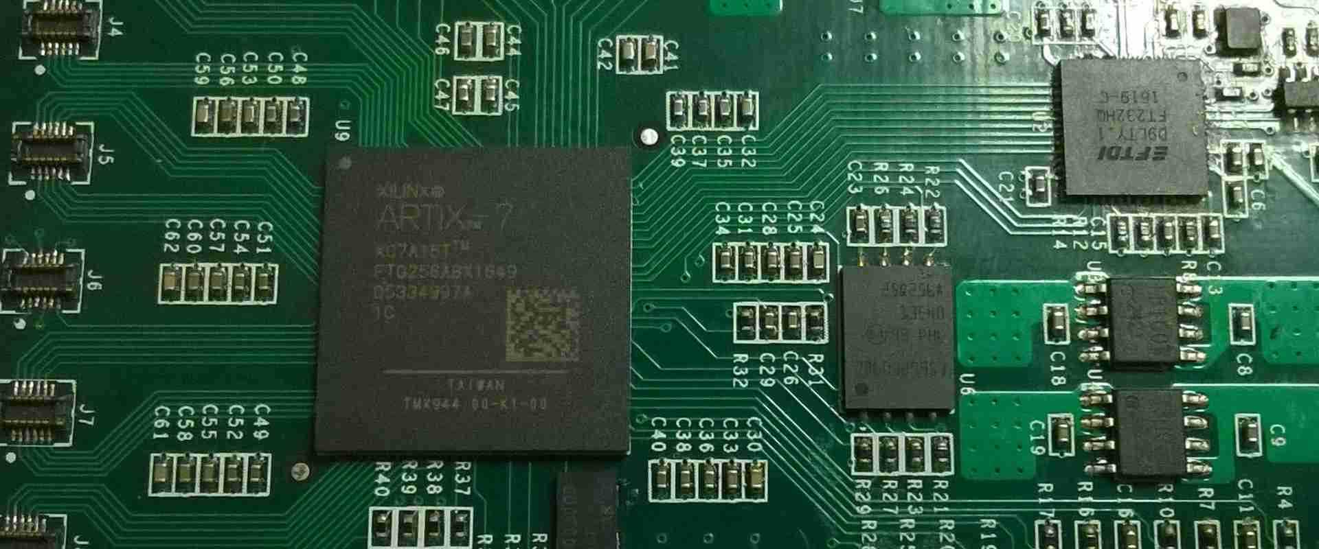
Solidworks PCB is a printed circuit board design software offered under the Solidworks brand, which is owned by Dassault Systèmes. It is tightly integrated with the Solidworks 3D mechanical CAD program, allowing users to design electronics and enclosures together in one unified workspace.
Solidworks PCB offers tools for schematic capture, PCB layout, component placement, design rule checking, and more. It generates manufacturing-ready outputs including Gerber files, NC drill files, assembly drawings, and IPC netlists.
As its name implies, Solidworks PCB is primarily marketed to existing Solidworks users. However, it can also be purchased as a standalone electronics design package.
Altium Designer
Altium Designer is a feature-rich PCB design tool developed by Altium Limited. It provides a unified environment for schematic capture, PCB layout, component management, signal integrity analysis, documentation generation, and FPGA design.
Altium Designer has a long history dating back to the mid-1980s. Over three decades of development, it has evolved into one of the most fully-featured and capable PCB design platforms available.
Whereas Solidworks PCB mainly targets mechanical engineers, Altium Designer is used by a wide range of professionals including electrical engineers, PCB designers, and embedded systems developers. It is an industry-standard electronics design solution.
Now that we’ve introduced both tools, let’s look at how they differ across some key categories.
Feature Comparison
The most significant differences between Solidworks PCB and Altium Designer come down to their respective features and functionality. Let’s compare them across some major areas:
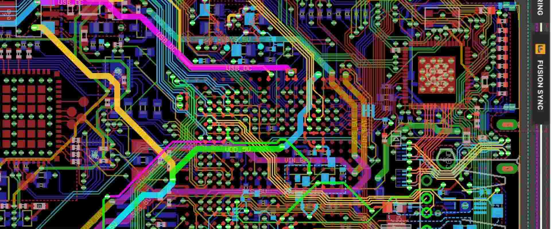
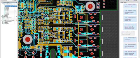
PCB Layout Tools
When it comes to PCB layout, Altium Designer provides more specialized and advanced capabilities versus Solidworks PCB.
Key advantages of Altium include:
- More customizable and automated routing options
- Interactive length tuning and matching for signals
- Extensive high-speed and differential pair routing tools
- Blind/buried via support and via stitching
- Sophisticated functionality for power planes and polygons
- Better support for rigid-flex PCB capabilities
Solidworks PCB has simplified routing that gets the job done for basic layouts. But Altium gives engineers finer-grained control and supports more complex PCB design challenges.
Library and Component Management
Both tools allow you to build custom component libraries and access integrated vendor libraries. However, Altium Designer has a clear edge when it comes to features and flexibility around part management.
Advantages of Altium include:
- Larger collection of ready-made manufacturer parts
- Ability to index external component databases
- Parametric components with full lifecycle support
- Part choice locking and revision tracking
- Parts for various design domains including FPGA, embedded, and multi-board
Solidworks PCB has sufficient components for common tasks. But Altium makes it easier to customize, organize, and reuse components across large enterprises and diverse design teams.
Design Reuse and PLM Integration
Altium also excels when it comes to supporting design data reuse and integration with product lifecycle management (PLM) systems.
Benefits include:
- Native integration with platforms like SVN, Git, and Teamcenter PLM
- Automatic linkage between schematics, layouts, and documentation
- Re-use of templates, macros, components, and sub-circuits
- Design variant and version management
- Support for manufacturing-ready data packages and handoff
By comparison, Solidworks PCB has lighter PLM capabilities focused mainly on integration with Solidworks CAD tools. The focus is more on managing individual PCB documents rather than enterprise-level design data.
Simulation and Analysis
Both platforms include tools for simulation and analysis to verify circuit behavior and PCB performance before manufacturing.
Altium Designer offers a wider array of options such as:
- SPICE, IBIS, and mixed-signal circuit simulation
- Power plane analysis for voltage drop and decoupling
- DFM analysis for manufacturability
- Signal integrity analysis for crosstalk and reflection
- 3D field solving for electrical and electromagnetic performance
Solidworks PCB covers the basics for simulation but once again has fewer advanced capabilities tailored to complex analysis.
Documentation and Outputs
Documentation is a key part of the design process. Both Solidworks PCB and Altium Designer can generate detailed drawings, schematics, BOMs, fabrication files, and other outputs.
Altium provides stronger documentation capabilities through features like:
- Customizable manufacturing documentation assemblies
- Automated BOM generation with supply chain linkage
- Automated PDF generation and report creation
- Scripting support for mass document production
- 3D PDF export for interactive visualization
As a CAD-integrated tool, Solidworks PCB excels at creating traditional engineering drawings. But Altium offers more flexibility for manufacturing files, BOMs, and intelligent documentation.
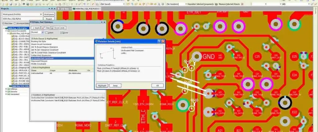
Design Rule Checking
Design rule checking (DRC) is an essential function that validates PCB layouts against fabrication constraints. It is used to avoid costly manufacturing errors.
Both Solidworks PCB and Altium Designer have robust DRC engines. Altium provides additional capabilities like:
- Rules can be customized using VBScript or JavaScript
- Supports length tuning rules for high-speed signals
- Per-net and per-differential pair rule settings
- Real-time and batch DRC checking modes
- Detailed reports to waive and document violations
Solidworks PCB has the basics covered for DRC. But Altium makes it easier to define detailed and advanced checking for complex boards.
Pricing Comparison
Another major difference between Solidworks PCB and Altium Designer is how they are licensed and priced.
Solidworks PCB pricing includes:
- Bundled with Solidworks CAD seat ($4,295 base price)
- Standalone license around $7,000 per seat
- Lower cost options for educational licenses
Altium Designer pricing includes:
- Subscription from $2,205/year to $7,900/year
- Perpetual license from $9,720 to $21,500
- Volume discounts available for teams
- Free limited functionality option
Solidworks PCB is very reasonably priced when bundled with Solidworks CAD tools. But as a standalone PCB solution, Altium Designer offers more flexibility including subscription options.
For large teams and enterprise customers, Altium Designer tends to provide greater value through volume discounts. But Solidworks PCB can make sense for smaller groups already bought into the Solidworks ecosystem.
User Interface Comparison
In addition to features and pricing, the user interface of each platform is worth considering.
Altium Designer uses a unified interface for schematic capture, PCB layout, library management, and other functions. Some benefits include:
- Consistent user experience across modules
- Live connectivity between schematics and PCB
- Highly customizable UI with dockable/tabbed panels
- Keyboard-driven workflow for speed and efficiency
Solidworks PCB has separate modes for schematic versus PCB editing. The interface will be familiar to Solidworks CAD users. Pros include:
- Integrates into Solidworks look-and-feel
- Clean, simple UI focused on core tools
- Easy transition for mechanical engineers
- 3D view link between electronics and enclosure
For electrical engineers doing heavy PCB work, Altium often provides a quicker and more tailored workflow. Solidworks offers a simpler interface targeting mechanical users.
Strengths and Weaknesses Summary
Based on the detailed comparison above, here is a high-level summary of the strengths and weaknesses of each platform:
Solidworks PCB
Strengths:
- Tight integration with Solidworks CAD
- Easy to learn for mechanical engineers
- Lower cost when bundled with Solidworks
- Sufficient for basic PCB layout needs
Weaknesses:
- Limited advanced functionality for complex designs
- Weaker library/component management
- Less flexibility around licensing models
- Less capable for large enterprises and teams
Altium Designer
Strengths:
- Very robust, full-featured PCB design environment
- Advanced tools for high-speed, RF, FPGA, flex, etc.
- Strong part creation/management capabilities
- Great for complex documentation and reporting
- Flexible licensing models to suit different needs
Weaknesses:
- Steeper learning curve than Solidworks PCB
- Overkill for simple or hobbyist PCB projects
- Can be more expensive as a standalone tool
As shown above, Altium Designer is the superior solution for advanced PCB work, but has a steeper price and learning curve. Solidworks PCB is a more basic tool, but benefits from tight CAD integration and bundle pricing.
Which Should You Choose?
With this exhaustive feature and capability comparison complete, should you choose Solidworks PCB or Altium Designer for your next project?
Here are some guidelines:
- If you already use Solidworks CAD, stick with Solidworks PCB for simplicity and bundle value. It can handle basic PCB needs when mechanical integration is a priority.
- For advanced electrical engineering work on high-speed or complex boards, Altium Designer is likely the better choice. It provides deeper functionality and tools tailored to the practicing PCB expert.
- If you’re part of a small team starting out, Solidworks PCB has a gentler learning curve and lower cost. Altium Designer scales better for large enterprises.
- For flexibility, Altium’s licensing model with subscription and perpetual pricing provides more options. Solidworks PCB access is tied to Solidworks bundles.
- Altium Designer has a steeper initial learning investment but can pay dividends on complex projects. Solidworks PCB is quicker to pick up but less capable for extensive designs.
The best option depends heavily on your specific needs. But this guide should help reveal the detailed pros and cons of each platform and guide your purchasing decision. Both Solidworks PCB and Altium Design offer compelling options—understanding their respective strengths is key to determining which solution makes the most sense for your next PCB project.
Frequently Asked Questions
What are the key differences between Solidworks PCB and Altium Designer?
The main differences are:
- Altium provides more advanced PCB layout tools while Solidworks PCB focuses on basics
- Altium has superior library/component management capabilities
- Altium integrates better with enterprise PLM/version control systems
- Altium offers more advanced simulation/analysis functionality
- Solidworks PCB pricing can be lower when bundled with CAD
- Altium provides more licensing flexibility including subscription
- Altium has a steeper learning curve but more powerful long-term capabilities
Which is better for mechanical engineers doing PCB design?
For mechanical engineers new to PCB design, Solidworks PCB is likely the better choice. It will feel familiar from using Solidworks CAD, and the integration between mechanical and electrical design makes collaboration easy. Altium Designer has a steeper learning curve for those without an ECAD background.
When does it make sense to choose Altium over Solidworks PCB?
Altium Designer makes more sense when you need advanced functionality like high-speed routing, differential pairs, RF design, or analysis features that Solidworks PCB lacks. The robust toolset of Altium is also preferred for complex or enterprise-level PCB work. When basic layout capabilities are sufficient, Solidworks PCB is a fine choice.
How does the pricing compare for small teams?
For smaller teams, Solidworks PCB can provide better value when purchased alongside Solidworks CAD tools. The bundle pricing is cost-effective for groups already using Solidworks. Altium Designer is price-competitive with Solidworks on a standalone basis through subscription licensing, but generally more expensive upfront on a perpetual license.
Can Solidworks PCB and Altium Designer work together?
While the tools have different native file formats, it is possible to convert files between Solidworks PCB and Altium Designer. There are reference guides available for moving PCB designs and libraries between the platforms. This allows some interoperability, though it’s best to pick one tool as the primary design environment.
Conclusion
Solidworks PCB and Altium Designer both provide capable PCB design environments with distinct strengths and target use cases. Solidworks PCB is simple to adopt for mechanical users and integrates smoothly with CAD. Altium Designer is the superior solution for advanced functionality and enterprise-level design teams, albeit with a steeper initial learning curve.
By understanding the in-depth comparison presented here between features, interfaces, pricing models, and intended users, both electrical and mechanical engineering professionals can make an informed choice between these leading PCB design platforms.
What is Solidworks PCB ?
SOLIDWORKS PCB delivers the needed productivity to quickly design PCBs. This is ensured with a unique partnership formed between 3D mechanical and electrical design teams. This provides a clear benefit where the ECAD-MCAD partnership is very important for the general success of the design of electronic products.
This PCB design system is easy to use. Also, it delivers a strong and effective set of design tools that help in developing some electronic products. This was designed to suit those that are new or not used to electronics design systems. SOLIDWORKS PCB 2020 provides a unique and refined design environment. Asides from this, they offer advanced features to ensure bidirectional interaction with the MCAD process.
By experimenting with the SOLIDWORKS PCB software, you can easily explore its features and interface.
The Environment of SOLIDWORKS PCB
SOLIDWORKS PCB integrates a lot of PCB design tools, which features an easy-to-use and modern design interface. It has a user interface feature, which supports a workflow that is smooth and intuitive. This can be seen in the PCB design solidworks, schematic, and even in the design release stage. These features include:
- A refined menu system of ribbon-style
- Multi-tab, flexible, design editor windows
- User configuration preferences
- Dockable panels, which helps when working with design documents
- A complete set of command shortcut keys
- web-based and context-sensitive help reference
While moving between tasks in the design workflow of SOLIDWORKS PCB, its system responds to the present requirements. It does this by opening the ribbon menu set, panels, and design editors, which you may need for the current task. The design environment maintains a consistent feel and look, and changes dynamically to present the right windows and tools as you design. The elements of the user interface are nevertheless consistent when it comes to function, positioning, and style.
- You can open multiple documents for editing, with each giving you a separate Document Tab, which can be found on top of the workspace.
- While switching between different documents, for example from a PCB design to a schematic sheet, the tool options, and ribbon menu will change automatically.
- The commands seen in the File tab of the ribbon remain unchanged, regardless of the type of document.
- Workspace controls like panels can be docked along any of the workspace’s edges, at the side, or float on top of the application.
Ribbon Command System
The ribbon-style menu of the SOLIDWORKS PCB offers a highly visual and dynamic control system. With this feature, you can quickly find the commands needed.
The arrangement of the menus and commands buttons are done in groups under some series of tabs, which will all change to work with the current task. What results is a command interface that is easy to use and efficient. This makes the best use of the screen space available.
Making use of the ribbon menu is just as easy as choosing the right tab, or flicking through them quickly to locate some commands suitable for your present needs.
To gain access to editing commands and common files easily, the ribbon menu includes a Quick Access Bar area which can be found above the ribbon tabs. It provides buttons to open as well as save a document directly. You can also use the redo and undo buttons for the edits you made last. The leftmost icon button of the SOLIDWORKS PCB offers window controls like Close, Minimize, Maximize, etc.
Start page
The start page of the SOLIDWORKS PCB is opened when you install the software for the first time. This offers a central location where you can access several system configuration options and system tasks.
The page is specially designed to provide a direct and simple way to gain access to the software’s routinely used areas
- To manage the software license of the SOLIDWORKS PCB, Select My Account. This will also help you to sign in and out, as well as change your Account Preferences.
- If you want to begin a new project (blank), or make use of one from the supplied templates list, click on Start a new PCB Project.
- To load a library or PCB project you have already started working on, click Open Project
- From the shortcut list of your recent projects, you can choose a project you have previously opened. You can then open it using SOLIDWORKS PCB.
- From the shortcut list of your Reference Projects, you can choose one of the reference projects. You can then open it using SOLIDWORKS PCB.
- To see your currently active project documents’ graphical preview, just click Project Documents. Then to open a document in SOLIDWORKS PCB, just click a preview twice.
- To install and access extension modules, which add to the functionality of the SOLIDWORKS PCB and software updates of the system core, click “Extension and Updates.”
Document Windows
When a document is opened in the major design window of the SOLIDWORKS PCB, it is now the active document seen in the associated editor.
You can open multiple documents simultaneously. Each of these documents has a selection tap, which can be seen on top of the design window.
The whole workspace can be occupied with documents. Also, you can share the workspace between many open documents through Split commands, which can be seen in the Window menu. You can then drag these documents from any split region to the other.
Reasons why you should choose SOLIDWORKS PCB

You can define the rigid-flex layer with angles and bend lines and validation with component clearance checking and 3D folding to ensure the correctness of the layout.
Data and Design Management
With the SOLIDWORKS PDM-based design, SOLIDWORKS PCB-PDM Connector, and the data management workflow, you can design files, manage projects, and make proper documentation.
You can also index and store and design data securely for quick retrieval. You don’t have to worry about data loss and version control. Also, it is possible to collaborate on design data from more than one location.
ECAD-MCAD Design Collaboration
The collaboration and integration of the ECAD-MCAD with SOLIDWORKS is unmatched. This unifies design data and enforces changes to both sides of the design project.
PCB Design Engine
It features an Altium-based, industry-proven design engine. This helps in the routing and layout of PCBs – printed circuit boards.
Modern Schematic Entry
The Altium solidworks has a schematic capture tool that has great and extensive electrical rules, libraries, and drafting capabilities.
Its Interface is Streamlined
It has an easy-to-use and intuitive interface. Asides from this, it has a use-model and consistent editor between the board layout and schematic capture.
The ECAD-MCAD Engineering Change Order (ECO) process is managed
A managed ECO process handles changes in design. This includes cutouts, mounting holes, component placement, and board shape. This ensures that designs are kept in sync.
3D Clearance Checking
Using components present in the mechanical composure, you can visualize the PCB. This is to help in reducing expensive prototypes by making sure that the board, as well as its components, is perfect for the mechanical enclosures with 3D clearance checking.
SPICE 3f5 Simulator (Mixed-Mode)
You can analyze and simulate mixed and analog-signal circuits from inside the schematic editor. This will help in preventing unnecessary design revisions and making design trade-offs by carrying out a functional validation on the designs before manufacturing or layout.
Supplier Links
Here, you can search online supplier links and databases or fix parametric data to the components of your design. This will help you match pricing, real-time device parameters, and availability. Asides from this, this equips you with updated information all through the whole design process.
By having this information, you will be able to make quick decisions to meet deadlines, budget, and electrical requirements.
Version Control
Compare and manage all the changes made and history to design files and gain higher control over the changes that have been made to your design. By this, you will know exactly what type of changes was made and who made them.
Component Database Support
From a corporate database, you can place the parametric data of the component directly. This keeps the components that have been utilized in your design synchronized with the database’s stored data.
Great File Support
With the 3D file support of SOLIDWORKS, you can be assured knowing the intentions of your mechanical designer. This offers a very pure and precise version of component enclosures and models. This makes sure that your check process offers a very good picture on board fit.
Revision Management and Design Commenting
Here, you can take total control of the process your design passes through and understand the changes made to the board design and the time it was made. Comprehensive design revision comments will let you see the history of changes made and with the ability to reject or accept the changes.
Conclusion
The SOLIDWORKS PCB design system is easy to use. It delivers a strong and effective set of design tools that help in developing some electronic products. Also, it provides a unique and refined design environment.