Step-by-Step Guide to PCB Design and Manufacturing

PCB Design and Manufacturing

Introduction

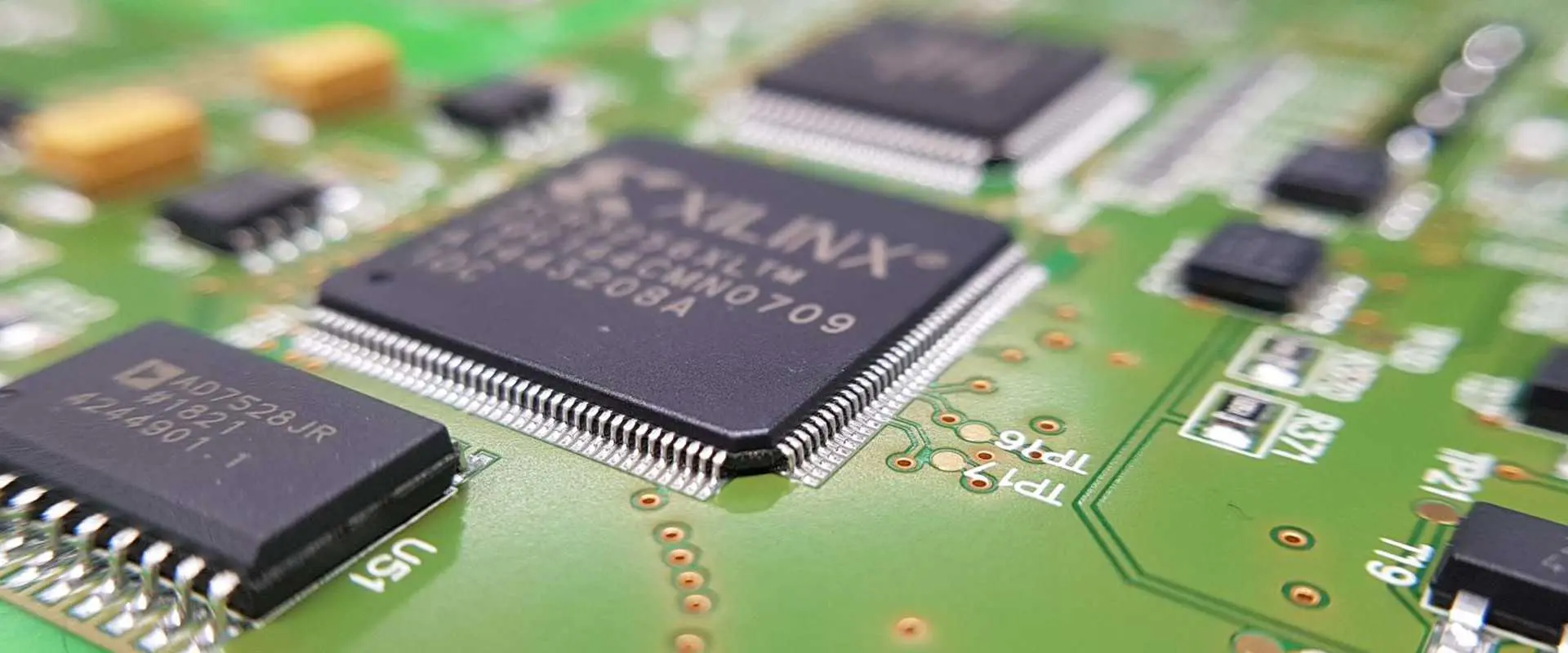
A printed circuit board (PCB) forms the backbone of an electronic product, providing the foundation to mount and interconnect components. Designing and manufacturing high-quality PCBs is a complex, multi-step process requiring expertise across electrical engineering, industrial processes, and quality control.

This guide will walk through the end-to-end PCB production process spanning design, fabrication, assembly, and testing phases. Understanding the big picture helps streamline executing each step smoothly. Weโ€™ll cover key concepts like schematic capture, layout considerations, generating manufacturing files, selecting materials and finishes, assembly methods, and inspection processes.

Letโ€™s get started on a step-by-step journey following a PCB from initial concept through volume production!

PCB Design Phase

Modular PCB Design
Modular PCB Design

Before manufacturing, a PCB design must be created and optimized. This frontend design process involves:
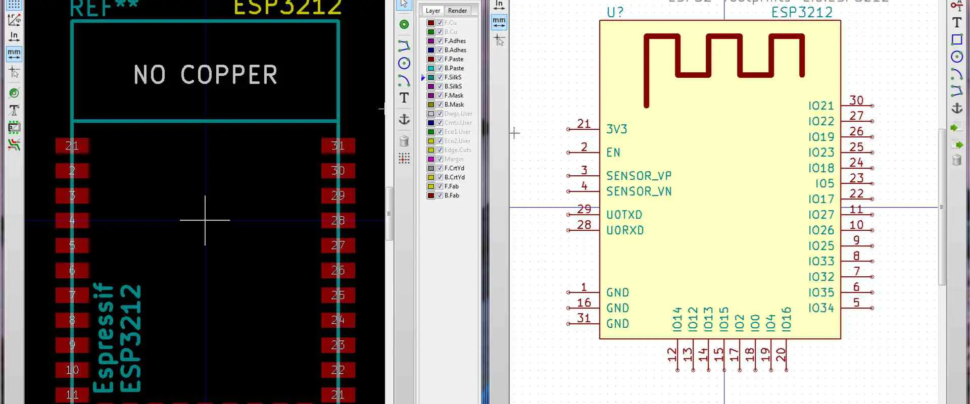
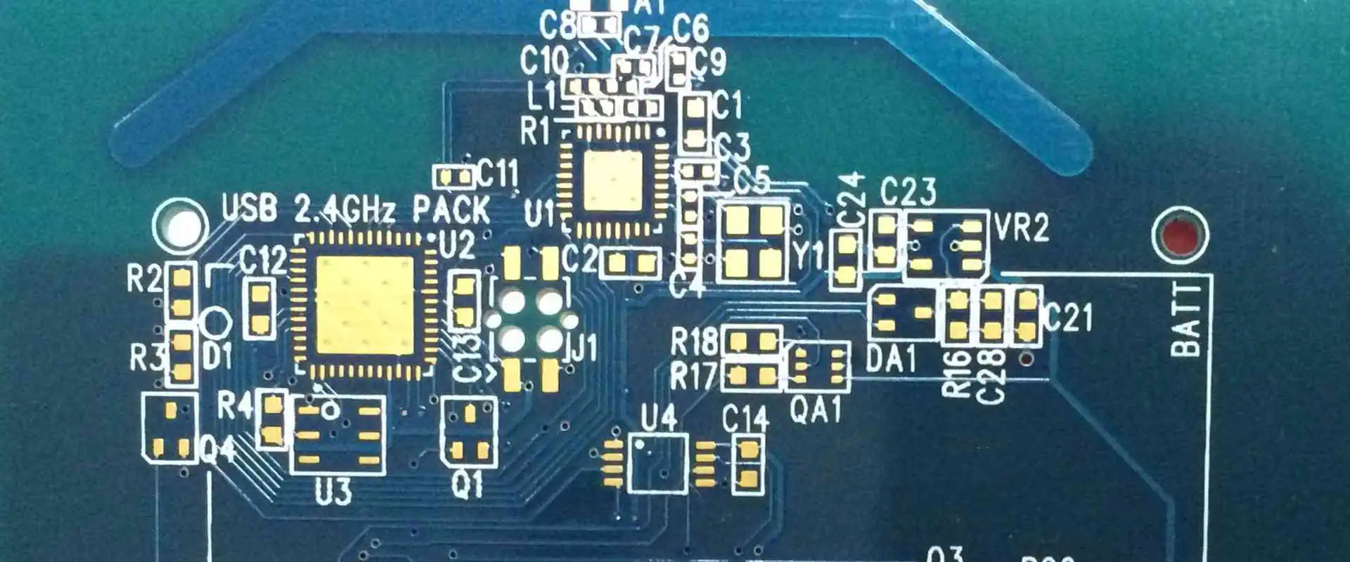
Schematic Capture

A schematic in CAD software connects symbolic representations of components logically using wires showing connectivity and net names. This turns an electrical concept into a virtual circuit diagram.

Simulation and Verification

The schematic gets simulated using SPICE models to verify proper component behaviour prior to physical layout.

PCB Layout

The schematic nets then get assigned physical connections and routed on board layers respecting electrical and physical design constraints.

Layout Optimizaton

The layout gets iteratively improved to enhance manufacturability, testability, and performance using guidelines like:

  • Component placement for efficient routing and assembly
  • Thermal management of heat-generating parts
  • Matching trace lengths and widths to signals
  • Minimizing loop inductance and maximizing decoupling
  • High-speed topologies like controlled impedance traces
  • Partitioning for panelization and board sections

Design Rule Checking

The finished layout gets programmatically checked against a myriad of fabrication and assembly rules to avoid both physical and functional issues.

3D Modeling

An optional 3D model of the board and components provides a realistic visualization of the final product.

With the design optimized, manufacturing output files are generated.

Manufacturing Data Processing

To fabricate and assemble PCBs, the design data gets processed into specialized formats like:

  • Gerber files – Standard files describing copper layers, solder masks, silkscreens, drilling info, etc.
  • Drill files – NC drill files with tools for all required hole sizes
  • Assembly drawings – Documentation for fabrication, test, inspection, etc.
  • BOM files – Bills of materials with part numbers, values, quantities
  • Netlists – Connectivity listings for assembly testing

Additional outputs like centroid data, testpoint reports, and IPC-2581 manufacturing archives help enable production. The data then gets transferred to the PCB fabrication facility and assembly house.

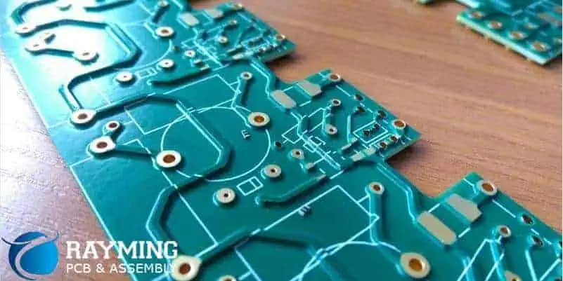
PCB Fabrication Process

The PCB fabrication process transforms the design files into physical boards ready for part mounting. Key fabrication steps include:

Substrate Preparation

The laminate substrate material gets conditioned through processes like cleaning, graining, desmearing, and via hole metallization.

Photolithography

A photosensitive dry film gets laminated onto the substrate then exposed to UV through the Gerber masks and developed to form the conductive pattern.

Copper Plating

The boards get electroplated to build up etched copper on exposed tracks to the target thickness defined in the design.

Etching

Chemical etching removes unwanted copper leaving only the desired conductive traces on the laminate.

Stripping and Etchback

The remaining photoresist gets stripped away and roughened copper gets etched back.

Soldermask

The soldermask layer gets laminated using the solder mask Gerber file exposing only solderable pads.

Silkscreen

Ink or epoxy graphics are applied for the silkscreen layer according to the silkscreen Gerber outline.

Surface Finish

The conductive traces get plated with solder, gold, or other finishes per specification to protect copper and facilitate soldering.

Routing

Mechanical routing cuts board outlines from the panel based on the fabrication drawing.

Testing

Bare boards get electrically tested against the netlist prior to component assembly.

The completed boards are now ready for part population by the contract manufacturer.

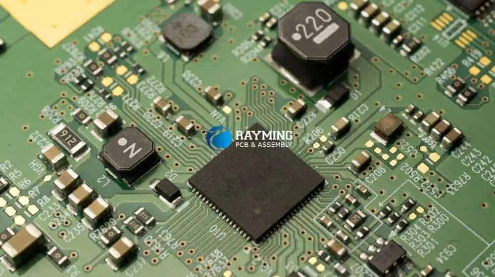
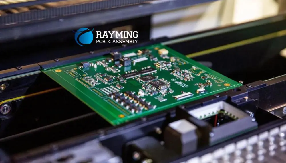
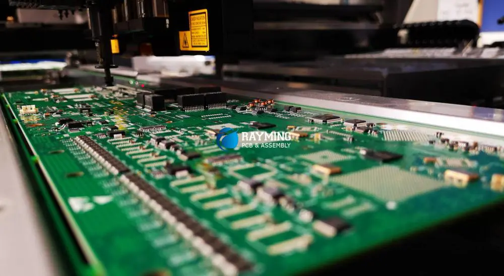
PCB Assembly Process

Consumer Electronics Assembly

Once fabricated boards are received, the assembly process populates components onto the boards. This involves:

Printing Solder Paste

Solder paste gets printed onto pads through a stencil aligned to the PCB.

Pick-and-Place Assembly

Robotic pick-and-place machines populate components onto pads according to the bill of materials and centoid data.

Reflow Soldering

The boards pass through a reflow oven melting the paste to form solder joints securing components.

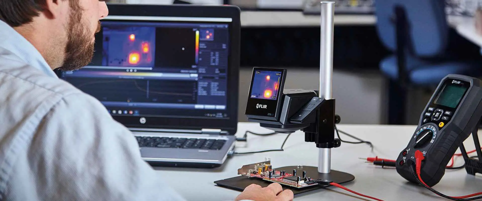
Inspection and Testing

PCBs get inspected for defects using automated optical inspection and other techniques, then tested for proper function pre-enclosure.

Conformal Coating

A protective coating gets applied to shield components from environmental factors.

Backplane/Daughter Card Assembly

For larger systems, boards and modules get mechanically assembled into card cages and rack infrastructure.

Enclosure Assembly

PCBs get integrated into plastic or metal product enclosures through alignment pins, clips, and fasteners.

This completes the board-level assembly process, with fully populated boards installed into final products.

PCB Manufacturing Quality

Throughout fabrication and assembly, quality standards are upheld through:

  • Statistical process control tracking defect and scrap rates
  • Extensive inspection checking operation output
  • Regular calibration and maintenance of machines
  • Conformance to stringent industry standards like IPC and ISO
  • Strict supplier quality management systems
  • Quality assurance oversight of manufacturing floor environment
  • Comprehensive testing of raw materials, in-process, and finished boards
  • Continuous improvement initiatives to drive down defects

Attention to quality ensures reliable, consistent PCB production.

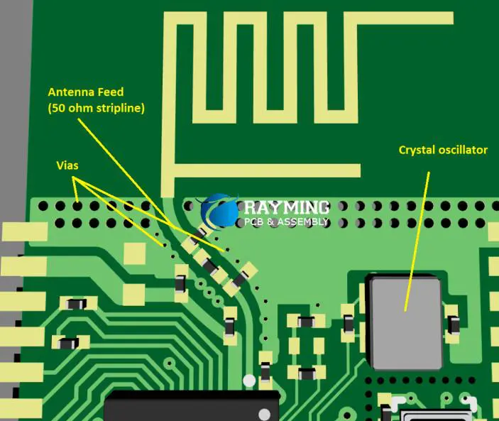
PCB Design Key Factors

To summarize, when architecting your PCB design, keep in mind these vital elements for manufacturing success:

Electrical

  • Component placement minimizing wire length
  • Trace widths matched to current
  • Controlled impedance on high-speed nets
  • Decoupling capacitance placed near ICs
  • Minimal antenna risks and crosstalk

Mechanical

  • Adequate clearance between traces and pads
  • Thermal relief to dissipate heat
  • Large pads and traces for higher current
  • Connectors placed with clearance for cables
  • Stress relief on components susceptible to vibration/shock

Manufacturing

  • Standard PCB dimensions for panel utilization efficiency
  • Test points designed for probing process validation
  • Component spacing within pick-and-place tolerances
  • Thermal profiles optimized for soldering
  • Assembly fixtures designed upfront

Getting the design right from the start smooths the entire downstream production process resulting in a functional, reliable, manufacturable PCB.

Conclusion

This comprehensive guide walked through the journey of a PCB from initial schematic design through factory fabrication, assembly, inspection, and testing based on real-world manufacturing processes. Understanding the sequence of steps provides helpful context for electrical engineers designing boards destined for volume production.

Key takeaways include laying out PCBs with manufacturing in mind, generating quality design data, communicating effectively with fabrication and assembly partners, and upholding rigorous quality assurance to ensure robust boards ready for installation in products. By following this PCB production roadmap, electrical engineers can transform ideas into fielded products reliably and efficiently.

Frequently Asked Questions

pcb-assembly-san-jose

What design practices help make PCBs easy to manufacture?

Some best practices include providing clearance between traces, avoiding tiny cutouts in planes, using standard component sizes and pitches, labeling layers clearly, and designing with the assembly process in mind through strategies like maximizing access to connectors and minimizing component height variations.

How long does PCB fabrication and assembly normally take?

For prototype volumes, fabrication can typically be completed in 5-10 days, with assembly requiring another 1-2 days. In production, fabrication lead times are usually 3-4 weeks, with assembly adding another 1-2 weeks. More complex designs may require even longer.

What are some key tests performed during PCB production?

Bare boards get electrically tested. After assembly, boards are visually inspected, undergo in-circuit testing, get programmed, experience functional validation testing, and undergo environmental stress screening through thermal cycling, vibration, and other techniques before shipping.

What tolerances should PCB layout accommodate?

Critical tolerances include solder mask registration (ยฑ0.075mm), hole position accuracy (ยฑ0.1mm), hole size variation (ยฑ0.075mm), conductor width and spacing (ยฑ0.075mm), and conductor thickness variation (10%).

How can I get quotations for PCB fabrication and assembly?

Reach out to manufacturing partners with your board files, BOM, target quantities, and any specialty requirements. Most will provide free assessments and quotations analyzing your design for manufacturability and providing estimated pricing.

Conclusion

Designing a board is only the first step – seamlessly navigating manufacturing processes transforms the ideas into reality. By understanding the progression from design to high-volume production, engineers can make decisions ensuring smooth fabrication and assembly resulting in functional, cost-effective boards. This PCB production primer provides helpful guidance for getting robust products to market.

Electronics rely heavily on printed circuit boards, as it helps in the transmission of electric signals to satisfy the deviceโ€™s mechanical and electrical circuit requirements. As such, printed circuit boards become indispensable to the proper functioning of electronic devices. Every economic sphere has increasingly relied on digitization, increasing the demand for computational electronics and thus PCBs.

PCB Design Manufacturing

As a circuit designer, the aspect of visiting and communicating your PCB designing and fabrication needs to a fabricator proves critical. However, physical visits have increasingly become impractical as major clients outsource their inquiries regarding PCB manufacturing needs to overseas manufacturers and suppliers. Therefore if you need a company to manufacture your design, you only have to contact them virtually. What’s more, online PCB design and manufacture instructions exist today, something that can become valuable if you want to design and produce one by yourself at home.  In this section, I intend to demonstrate the relevant processes of PCB manufacturing to help you design and produce printed circuit boards.

Process Steps

Once completed and approved, the PCB design can now go into production. As the designer, you have to export your design in a suitable format that the manufacturer can support. One renowned and agreeable output format is the Gerber. Additionally, please note that diverse PCB design and manufacturing tools require distinctive generation steps of the Gerber file. It encodes all-inclusive and important information that includes drill drawing, copper tracking, component notations, apertures, etc. All the design aspects undergo checks at this stage, where the program executes oversight algorithms to make sure that no errors pass undetected. At this point, you can also study the plan, especially aspects like the spacing of the board edge, track width, hole, and track spacing, besides hole size.  After that, the PCB design can then get forwarded to manufacturers like RayMing PCB & Assembly. Here, the DFM gets carried out to ascertain that the PCB design meets the minimum tolerance requirements under production.     

pcb designing and fabrication
  • Conversion from the file into film
  • Once you have developed the schematic files and the manufacturer also completes the DFM check successfully, printing can start. Most manufacturers use a plotter to develop photo films, instrumental in the printing of the circuit boards. The films get used for imaging the PCBs by the laser printer, proving incredibly precise in providing a detailed film.  

What results from the process includes a unique plastic sheet complete with a black-inked photo negative. The black ink denotes the PCB’s conductive copper segments, while the clear part represents the non-conductive material. A similar pattern happens for the outer layer though this happens in reverse: clear denoting copper and black denoting the segment to get etched away.

Every solder mask and PCB layer gets its black and clear film sheet, and this implies that a double-layer PCB will require four sheets. Remember, all the sheets have to get used with one corresponding to the other. Additionally, you have to punch registration holes through every film to realize a perfect alignment.

  • The inner layer’s printing process
  • Here, the intention entails printing the mapped-out copper path created on the film on a foil of copper. It acts as a preparatory step in the PCBโ€™s manufacturing process. The laminate, composed of fiberglass or epoxy resin substrate, acts as an ideal platform to receive the copper, which provides structure to the PCB. It not only provides a platform but a dust-resistant and sturdy material to support the PCB fabrication. Since copper proves pre-bonded on either side of the substrate, this process entails whittling it away to divulge the design.

Cleanliness becomes a crucial part of the PCB construction process, and thus, the copper-sided laminate has to get cleaned and passed through a decontaminated. During the decontamination process, avoid any dust particles from settling on the PCB laminate. Otherwise, it can end up making the circuit short or open.    

In the next stage, the panel gets a photo-sensitive film layer called the photoresist. It comprises elements that end up toughening upon exposure to UV. It ensures a perfect match in the photoresist as it had proved on the photo film.

After preparation, the board must get washed with an alkaline liquid to eliminate all the unhardened photoresist. Subsequently, the pressure wash that follows will leave the surface spotless and free from anything remnants. It then undergoes drying before another round of examination by a technician to eliminate errors. Remember the step applies to multi-layer boards only.

  • Removal of unwanted copper. The next stage entails the elimination of the unwanted copper using a copper solvent liquid. Remember the weight of the board determines the quantity of solvent used.  Another round of washing happens after the removal of the unwanted copper. Here, the hardened resists safeguarding the desired copper gets washed off. You will end up with the glistening copper substrate needed for the printed circuit board.
  • Optical inspection and layer alignment
  • Now the layers prove clean and ready to punch the alignment holes to ensure a proper alignment. The next step in this stage entails aligning the registration holes of both inner and outer layers. The layers get optically punched to allow exact correspondence.  Remember, once placed together; the layers cannot get corrected for any inner layer errors. Because of this, another round of automatic optical scrutiny to ensure the panels are free from defects. Here, the Gerber acts as the standard and digitally compares the image with the original. Any inconsistency gets displayed for immediate attention, and once it passes the test, it moves to the final phases of the printed circuit board production.
  • Layer up before bonding. All the different layers get fused, with the outer layers joined with the FR4/substrate. The process has a two-step process of fusing the substrate with copper. The next step entails bonding where the layers get fit on the table-attached pins. It becomes crucial to secure it snuggly and avert shifting when aligning.  Once every layer gets fit and layered properly over each other, you can now go ahead with pressing. The process gets carried out by a bonding-press computer that determines and organizes the automatic heating besides determining the pressure points to act on. It then follows an unpacking process after every layer gets molded together to form a PCB sandwich. Here, the pins used to restrain the board gets removed, and the upper pressure plate is discarded.     
FULL PCB MANUFACTURING Quote
  • Drill. It entails boring holes into the board stack. The minuscule nature of the holes demands precision, as every other component that comes later depends on this precision. The drill target location gets determined by an x-ray finder before drilling and subsequent hole registration.  Additionally, the micro-movement of this drill gets controlled by a computer, which controls the movement by using prior design details. The extra copper lining the edges gets removed using a profiling device.
  • Copper deposition and plating. It is the next step after the drilling process. Here, you get a fusion of diverse layers using chemical deposition. After that, the panel has to go through subsequent chemical baths, with each bath depositing a thin copper layer on the panelโ€™s surface, covering the new holes.  
  • Imaging of the outer layer. It involves applying the photoresist again, though it concentrates on the PCB panel‘s outer layer. It has to go through a similar process explained earlier to gain the toughness. Further, black ink film gets held by pins in preventing any misalignment until after exposure to high UV rays. After that, any unhardened resist material gets removed.
  • Plating. The plating process proves similar to the one illustrated in the eighth step. It entails electroplating with copper before a subsequent plating with tin. It will allow the elimination of extra copper left. Further, the tin safeguards the panel section that remains encased in copper in the subsequent etching stage. Etching always removes any undesirable copper foil on the panel.
  • Final etching. The tin layer safeguards the copper during this phase, where the undesired copper (including from beneath any resist layer) gets removed. Chemical solutions get applied to eliminate the extra copper. At this point, all the connections and conducting areas prove properly established.
  • Application of the solder mask. Clean and cover the panel with epoxy solder ink before applying the solder mask. After that, it receives another UV light blast that toughens the uncovered segments while the covered and soft segments await removal. It then has to get heated to cure the applied solder mask.
  • Surface finish. In this stage, the application of silver and gold coats happens, which incorporates additional solder-ability.  Additionally, hot-air leveling ensures uniform pads and leads to surface finish generation.
  • Silkscreen. The almost complete board has to receive an ink-jet surface writing to indicate crucial details concerning the printed circuit board. It then passes through the coating and subsequent curing phases.
  • Electrical test. It then becomes crucial for the PCB to undergo an electrical test as the ultimate precaution.
  • V-scoring and profiling represent the last process where the board gets cut using a v-groove or router.

The Vital Details about Button PCB

Button PCB

The importance of circuit boards to the functionality of electronics cannot get stated enough. It ensures proper mechanical and electrical signaling within the circuit. However, circuit boards come in many forms and types, and it cannot surprise me if you have never heard of a button PCB. The PCB comes as an uncommon type, complete with a circuit board button. Therefore, if you love circuit boards, perhaps it would do you some good to dig and understand this printed circuit board.

The Button Printed Circuit Board

Button PCBs have widespread application, and perhaps because of the simplicity of their application, not many people know how often they interact with them. The simple yet effective PCB button pad example includes everyone inadvertently using a remote control device. Rings a bell now? A button PCB contains a markedly visible coil pattern, all crucial single-layer PCB components, but besides these, it also possesses buttons to complete or break circuits.

Inner Dynamic of a Button PCB You Must Know

pcb circuit board button

Many individuals, including experienced PCB designers and manufacturers, often prove unaware of how a button-printed circuit board works. To understand this, imagine a product with the capacity to sense and react to the immediate surrounding. Such a product will need the correct components to make it operational. If this product involved a circuit board, then one of these key components would become a switch.

Switches come under two categories of โ€œoffโ€ or โ€œon.โ€ The โ€œoffโ€ implies that you must turn the switch โ€œonโ€ while the “on” switch always stays in a single mode. PCB buttons, therefore, get inferred as on/off switches. Consequently, such a printed circuit board gets referred to as a power button PCB.

A button PCB proves popular for electronic projects, primarily as a PCB layout. The component layout of such a PCB layout gets deployed in the fabrication of buttons. Therefore, you should not get surprised to discover its importance in controlling the digital touch knob. It uses a simple pushbutton to key in data when pressed and uses a LED matrix in displaying information.  

A button PCB contains diverse features, including multiple interface types that allow it to get powered off or on, resetting it, or determining anything else you need to perform.  It also contains four LEDs that prove programmable, where you can program them with different colors besides timing restrictions.

The Button PCB has many different features, including multiple interfaces that enable the user to turn it on or off, reset it, or generally determine what they want it to do. The Button PCB also has four LEDs (light-emitting diodes) that can be programmed with different colors and timing restrictions for RGB lighting effects.

A button PCB comes as a small and standard circuit equipped with a power supply system that accepts wall adapters and batteries when it comes to powering your device. Therefore, it got developed to allow individuals to deploy them for their additional circuitry needs and personal use. Moreover, since a button PCB programming process proves simple, it acts as an incredible device for learning and prototyping circuits without investing further.

How a Button PCB Works

Here, it becomes instrumental in plugging the device into a button PCB before connecting the wires emanating from your power cables to each input pin. For powering low-voltage devices such as the sine wave, deploy a single wire for every button. However, if you have to power high-power devices, then dual (two) have to get fixed to each button. For instance, if you have three wires for powering the RGB LED strips, you should use two of the wires for the “on” and a single one for the “off” button. The outcome will encompass cutting off the power to a selected device when you get to press that button. Consequently, it makes the automation of homes easy while computer hacking also becomes more convenient. For instance, you can decide to program your home’s button PCB to switch on the lights when you leave the house and back on when you enter.

PCB touch button and socket

The pcb touch button, which is usually completely encapsulated in a plastic case, contains the actual electronics and controls the button’s opening and closing action. The pcb touch button can be used as a standard button. It can also be configured to produce customized clicks via embedded software. The contacts that plug into your device are often located at or near the bottom of the PCB. This is due to how shallow the PCBโ€™s cavity is in order to maximize area for the touch button and minimize space needed for its components. This means that the buttons are laid out in a way that makes them easier to manufacture or assemble.

Vital Terminologies Used in Button PCB

  • Circuit board button. It represents a modest circuit that comprises limited components like the LED, button, and resistor R1. Some instances see an IC (integrated circuit) which acts as the circuit controller. A controller gets deployed as a blend with further circuits and printed circuit boards that it regulates. You can connect components to the PCB or opt to solder them. Whenever you press the PCB button, you short-circuit the IC pins and trigger specific responses. Upon release, the integrated circuit pin connection breaks, and therefore it will no longer respond.   

It also becomes crucial to present some vital concepts like the touchpad, power supply pin, and a PE circuit. If you use these concepts, designing a stable printed circuit board with an enhanced outcome becomes a reality.

  • Printed-electrolysis circuit (PE). It is a circuit that gets primarily used to supply power to your button pad. It often proves concealed between the copper plate and the silicon rubber. The PE utilizes the electrolysis in generating the 5V power via the copper and other elements (chemical) contained around that spot. Therefore, you have no cause to stress about proving an unknown quantity as its operation proves simple to comprehend. Additionally, it is similar to other chemical reactions.
  • The power supply pin. It comes as two copper pads, with one acting as the ground and the other the positive. The pads are located in the middle of the printed circuit board. It functions as power supply conduits to the integrated circuit or BP (button pad). However, it also becomes necessary to avoid confusing the pins with the GND connection as they possess a lower voltage compared to normal PCB buttons. ย Therefore, you cannot deploy it to supply power by connecting it to the IC directly. Consequently, the existence of a PE circuit becomes essential, especially in dealing with this challenge. ย ย 
  • Touchpad. It becomes essential to get familiar with touchpads, especially after building a printed circuit board. A touchpad denotes the area responsible for sensing any finger touch. The area gets isolated from other adjoining areas (from 50% to 100%) to provide an almost zero parasitic capacitance. It is for this reason that it gets inferred to as the touchpad. Typical touchpads come as one-layer, two-layer, and three-layer printed circuit boards, with diverse characteristics.

Caution

FULL PCB MANUFACTURING Quote

It becomes crucial to avoid creating the circuit for your touchpad, especially if you make printed circuit boards. The reason lies in the complexity involved. For instance, placing plenty of capacitors on a parallel arrangement will lead to an incidence of parasitic capacitance, where these tally up fast to create a high-impendence input (where the capacitors turn into equals with one another). Consequently, your printed circuit board will end up malfunctioning. It proves a typical problem that most people experience with their circuits as it becomes stuck)

As an astute PCB designer, it becomes crucial to comprehend a PCBAโ€™s power supply pin well. It will help you avoid the prevalence of working with unstable PCBs. Additionally, the highly-impedance touchpads demand careful consideration from you.

However, if you cannot go about this the correct way, then it will become ideal to contact and outsource the services of RayMing PCB and Assembly Company to create such a complex touchpad for you. You will get quality guidelines on the ordering process on their website and get a fair deal within a reasonable time. What’s more? You will get excellent customer service as you await your touchpad circuit.

In short, it becomes instrumental in understanding everything concerning PE circuits besides the power supply pin contained in PCBs, especially for people who yearn to design and handle printed circuit boards. You then have to design your intended signal output in line with the relevant rules to ensure you keep it stand and working every time. ย ย 

Final Thoughts

In the article, we have enclosed some elementary details concerning the button-printed circuit boards and, by extension, the PCB industry. We have shared all the necessary details to understand some typical challenges predominant in the world of button boards. Therefore, if you hold an interest in making your design, do not fail to focus on these crucial points. Additionally, if you have questions, you can always visit RayMing PCB and Assembly company website to get more details about printed circuit boards, procuring these services and products, and understanding circuits in general. Happy reading.

Top 25 SMT Companies in 2023

smt company

Introduction

Surface mount technology (SMT) has become the predominant method for assembling printed circuit boards (PCBs) in electronics manufacturing. Utilizing robotic pick-and-place machines to populate boards with surface mount components enables highly automated assembly with miniaturized components.

Hiring an experienced surface mount assembly services provider is crucial to guarantee quality and reliability for an electronics product. This article will explore the top 25 companies providing SMT manufacturing globally based on factors like capabilities, reputation, scale, and technology leadership.

Read on for an overview of the top contract manufacturers advancing the state of the art in surface mount productions, as we count down the top 25 SMT companies in 2023.

Ranking Methodology

through-hole assembly process

Companies were evaluated and ranked based on the following key criteria:

  • Technical capabilities – SMT line diversity, maximum board size, component size range, and other production capabilities demonstrating advanced technical competence.
  • Geographic reach – Number of manufacturing locations, countries, and regions served demonstrating global scale and presence.
  • Certifications – Holding demanding certifications for quality management and environmental standards from bodies like ISO, IATF, and others.
  • Industry reputation – Feedback and recommendation from electronics industry experts, customers, and associations gauging SMT quality and reliability.
  • Technology adoption – Use of innovative techniques like AOI inspection, 3D solder paste inspection, automated optical shaping, and more cutting-edge automation.
  • Key customers – Experience serving premier electronics brands with demanding high-volume production needs.

With these criteria in mind, here are the top 25 global surface mount technology assembly providers in 2023:

#25 – VTech EMS

  • Headquartered in Dongguan, China
  • 10 manufacturing facilities across China
  • Diverse electronic product expertise including consumer, telecoms, medical, automotive, IoT
  • ISO 13485 and ISO 14001 certified
  • Services from PCB assembly through full box build support

#24 – altus AG

  • Based in Germany with factories across Eastern Europe
  • Focus on automotive, transportation, industrial, and medical customers
  • Ample SMT lines featuring Fuji NXT and AIMEX equipment
  • Rigorous quality control standards per ISO 9001, ISO 13485, IATF 16949, and more
  • High mix/low-mid volume manufacturing ideal for European regional support

#23 – Suntsu Electronics

  • Taiwanese EMS company with sites across Asia
  • Broad capabilities for consumer electronics, computers, peripherals, and communications equipment
  • SMT production using latest Yamaha and Juki machinery
  • Veteran provider serving customers for over 25 years
  • Robust quality certifications including ISO 9001, ISO 13485, ISO 14001

#22 – New Kinpo Group (Cal-Comp)

  • Headquartered in Taiwan with dozen manufacturing sites across Asia and Mexico
  • Massive capacity with 100+ SMT lines and over 15,000 employees
  • Focuses on computers, networking gear, consumer electronics, IoT, and smart home products
  • Industry 4.0 initiatives around automation, analytics, and smart factory
  • Joint design and manufacturing services under one organization

#21 – Zollner Elektronik

  • German full-service EMS provider with factories across Central Europe
  • Diverse industry expertise in industrial control, medical, measurement, automotive, aerospace, and engineering services
  • Comprehensive quality management system certified to multiple ISO and industry standards
  • 300+ injection molding machines and fully automated SMT lines featuring Fuji AIMEX equipment
  • Renowned for high-mix, high-complexity, and flexible production

#20 – SIIX

  • Subsidiary EMS division of Japanese conglomerate MinebeaMitsumi
  • Global manufacturing presence across Asia, Europe, Mexico, and Brazil
  • Scale to produce up to 500 million PCB assemblies per year
  • Highly automated production using latest Yamaha SMT equipment
  • Broad capabilities serving aerospace, defense, telecoms, networking, IoT, and automotive verticals

#19 – Fabrinet

  • Headquartered in Thailand with sites across Asia Pacific
  • Foundry model providing optimized flexibility and speed
  • High complexity PCBs with 01005 components and 0.3mm pitch BGAs
  • Smart factory initiatives include automated optical inspection, 3D solder paste inspection, and advanced analytics
  • Large optics manufacturing capabilities supporting camera modules, LiDAR, sensors

#18 – Key Tronic

  • Global sites across North America, Europe, and Asia
  • Leading medical, aerospace, automation, and computing ODM services
  • Collaborative design engineering engagement for manufacturability
  • Quality certifications include ISO 9001, ISO 13485, AS9100D, and IATF 16949
  • Diverse precision electromechanical, plastics, and metal fabrication capabilities

#17 – hiking (Kin Yip)

  • Headquartered in Hong Kong with sites across Asia
  • High-complexity, high-reliability manufacturing
  • Specializes in consumer, communications, automotive electronics
  • Highly automated production with 3D AOI, 3D SPI, component traceability
  • Certifications include IATF 16949, AS9100D, ISO 13485, ISO 14001

#16 – Enics

  • Swiss EMS provider with sites across Europe and Asia
  • Diverse expertise in industrial, automotive, medical, aerospace/defense, instrumentation, and building technologies
  • Focus on low-mid volume, high-mix production
  • Certified for ISO 13485, IATF 16949, AS9100, ISO 14001
  • Design support, NPI, and aftermarket services under one roof

#15 – Sumitronics

  • Japanese EMS founded in Malacca, Malaysia with sites across Asia
  • Scale of 500 SMT lines producing over 100 million PCBs annually
  • Broad capabilities serving computing, consumer electronics, communications, automotive, industrial
  • Investments in smart factory automation technologies
  • Certified for ISO 9001, ISO 14001, ISO 13485, IATF 16949

#14 – Ducommun

  • Global EMS headquartered in Southern California
  • Provides advanced integration and system-level assemblies for aerospace/defense, space, and industrial technology
  • Leading expertise for high-reliability, high-complexity designs
  • AS9100D and Nadcap accreditation at all sites
  • Design engineering collaboration and NPI

#13 – Jabil Circuit

  • One of the largest and most geographically diverse EMS providers
  • Over 25 million square feet of manufacturing space worldwide
  • Expertise across defense, aerospace, automotive, healthcare, computing, storage, and packaging verticals
  • Design support services augmented by automated DFM analysis
  • Top certifications like IATF 16949, ISO 9001, ISO 13485, AS9100

#12 – Natel Engineering

  • Silicon Valley contract manufacturer founded in 1974
  • Highly automated SMT production with 3D AOI inspection
  • Leading medical, industrial, aerospace/defense, instrumentation expertise
  • Natel Design Services team aids product development
  • Certified to ISO 13485, ISO 9001, AS9100

#11 – Creation Technologies

  • Global EMS headquartered in Canada with sites across North America and Europe
  • Diverse expertise across consumer products, telecoms, medical, test and measurement, cleantech
  • Vertically integrated plastics, precision metal, and final assembly
  • Design for manufacturing analysis and NPI launch support
  • Certifications include ISO 9001, ISO 13485, IATF 16949, AS9100

#10 – Flex Ltd.

  • Global EMS giant with sites across 30 countries
  • Massive capacity of over 100 million square feet of manufacturing space
  • Leading aerospace, automotive, computing, consumer, health, industrial capabilities
  • Flex Enablement Program provides manufacturing input starting from early design phases
  • Top certifications like ISO 13485, IATF 16949, AS9100

#9 – Benchmark Electronics

  • One of the largest US-based EMS providers
  • 8 million square feet of manufacturing across Americas, Asia, Europe
  • Diverse expertise in medical, aerospace/defense, computing, telecoms, test and measurement, controls
  • Benchmark Operational Excellence drives quality, reliability, and efficiency
  • Certified to ISO 9001, ISO 13485, AS9100, IATF 16949

#8 – Sanmina Corporation

  • Global EMS leader based in California with sites worldwide
  • Massive technology portfolio spanning high-tech industries
  • Scale of over 5 billion components managed and 2 million PCBs shipped per day
  • Innovations in digital twin, predictive maintenance, and analytics
  • Certifications include ISO 14001, ISO 13485, AS9100, IATF 16949

#7 – Kimball Electronics

  • Top global EMS founded 1967 and headquartered in Indiana
  • Specializes in automotive, medical, industrial, and public safety markets
  • 8 million square feet of manufacturing across facilities in US, Mexico, Poland, Thailand, China
  • Collaborative product lifecycle management and value-engineering
  • Certified to IATF 16949, ISO 9001, ISO 13485, ISO 14001

#6 – Plexus Corp.

  • EMS innovator founded in Wisconsin in 1979
  • Leading expertise in medtech, defense and aerospace, industrial, networking, and telecoms
  • Engineering solutions across full product lifecycle
  • Smart factory initiative optimizing IoT, automation, visibility
  • Certified to AS9100, ISO 13485, ISO 9001, IATF 16949

#5 – Foxconn (Hon Hai)

  • The worldโ€™s largest electronics manufacturing giant
  • Unparalleled scale as a key Apple, HP, Dell, Nintendo, Sony partner
  • Massive production capacity across China and India factories
  • Highly optimized automated assembly lines
  • Rigorous quality control for premier consumer brands

#4 – USI Electronics

  • Headquartered in Taiwan with sites across Asia
  • Leading high-precision SMT capabilities
  • Diverse expertise across networking, telecom, medical, industrial, automotive
  • Design, systems integration, logistics, and aftermarket repair services
  • Global certifications include IATF 16949, ISO 13485, TL 9000

#3 – Pegatron

  • Spun off from Asus as a leading EMS focused on quality, flexibility, delivery
  • Scale of over 40 million square feet of manufacturing space
  • Key manufacturing partner for global computing brands
  • Stringent process control with automation and AI
  • Certified to ISO 14001, OHSAS 18001, IATF 16949

#2 – Quanta

  • Global EMS leader headquartered in Taiwan
  • Premier ODM partner for top computing, networking and telecom brands
  • Unmatched expertise and capacity optimized for high-volume production
  • End-to-end manufacturing including components, modules, and final assembly
  • Industry 4.0 initiatives such as AI quality inspection

#1 – Rayming Technology

  • Founded in China in 2002, now a leading global EMS provider
  • Flagship facility in Dongguan spanning over 6 million square feet
  • Complete range of electronic manufacturing services
  • Highly automated SMT production with 3D AOI and SPI
  • Rigorous quality system certified to ISO 13485, ISO 9001, IATF 16949

Key Takeaways

This list of the top 25 SMT assembly companies provides a benchmark of premier manufacturing partners serving diverse industries. Key takeaways include:

  • Leading providers offer unmatched expertise, capabilities, scale, and certifications
  • Global sites provide regional manufacturing options and supply chain resilience
  • Automation, analytics, and smart factory initiatives drive continuous advancement
  • SMT leadership enables the ongoing electronics revolution in every sector

For those seeking an experienced surface mount assembly partner, this list offers a framework of the top-tier EMS leaders delivering manufacturing excellence worldwide. SMT competence underpins nearly all cutting-edge product development today. By collaborating with these leading innovators, electronics companies can bring robust, reliable products to life.

Frequently Asked Questions

What are some key SMT capabilities to look for in a CM?

Top capabilities include 01005 and microBGA assembly, advanced AOI inspection, proficiency with high-density PCBs, extensive DFM analysis, thermal process expertise, flexibility with low to high volumes, and turnkey box build support.

How can I evaluate an SMT company as a potential partner?

Tour facilities to witness capabilities firsthand. Review industry certifications and quality procedures. Discuss your specific project needs and assess responsiveness. Request referrals from existing customers. Start with a small test order first before ramping up.

What emerging technologies are impacting SMT manufacturing?

Key trends include data analytics, machine learning inspection, collaborative robots, digital twin simulation, augmented reality visualization, additive processes like printing, and overall smart factory connectivity.

How are lead times at SMT companies lately?

Due to component shortages and supply chain issues, lead times have been extended significantly – often over 20 weeks currently from order to delivery. Careful planning is crucial.

What questions should I ask prospective SMT partners about quality?

Inquire about defect rates, soldering process controls, quality certifications, employee training procedures, repair/rework/scrap rates, traceability practices, and continuous improvement strategies aimed at driving defects to zero.

Conclusion

As consumer appetite for sophisticated electronics continues to accelerate, partnering with an exceptional SMT manufacturing provider becomes crucial. This list offers a guide to the most capable global assembly houses leading the evolution of surface mount technology into the future. By leveraging the expertise of these elite SMT innovators, engineers can transform designs into products with the quality and reliability end users demand.

Overview of the SMT Market

The SMT industry represents a sizeable, lucrative, and growing market with an estimated value of USD 5.42 billion by 2022. It arises from the increasingly on-demand need for printed circuit board miniaturization. The five-year period forecast by category that started from 2017 offers better insights.

  • By equipment
  • The inspection equipment category represents a significant SMT market category with a 28% market share. It is a market class that gets propelled by the ever-improving product tech, reliability, responsiveness, and inspection quality. Increased demand during the forecast period is especially accounted for by the automotive, telecom, consumer electronics, computing, and storage.
  • By application
  • In the forecast period, the application segment of consumer electronics gets expected to account for the lion’s share of the SMT market. The demand gets propelled by the increasing preference for small-sized devices, in which SMT technology plays an instrumental role. SMT components prove small, lighter, and thinner compared to through-hole packages.
  • APAC. It gets estimated that it will account for the lion’s share when it comes to market size. The projection also entails rapid growth during this five-year forecast period, accounted for by the telecommunication sector. The key driver for this SMT segment entails the growing demand for the 3G/4G networks. Companies within this market segment deploy growth approaches like fresh product launches, agreements, collaborations, partnerships, and acquisitions.      

Overview of an SMT Company

A surface mount technology company infers a company within the PCB electronics industry that provides SMT products and services. While some of these companies specialize solely in surface mount technology, most tend to deliver products in the broader category of printed circuit boards. However, these companies still provide SMT and SMD products through their qualified teams of engineers and designers.

The SMT company not only has to possess the required financial and human resource capacity to deliver quality SMT devices but prove licensed to operate by the relevant authorities besides having a demonstrated history of working on printed circuit boards and surface mount technology. These companies’ products and services often include SMDs (surface mounted devices), SMT software design tools, manufacturing, and assembly services.

An excellent example of an SMT company includes the RayMing PCB and Assembly Company. The company has its base in China and has a fifteen-year demonstrated track record of providing state-of-the-art PCB tech products and top-rate quality standards in the electronics industry. It prides itself in meeting your PCB demands, including SMT products and services. It starts from the small volume level to mass PCB production, regardless of the simplicity or complexity of your design.

Features of a Surface Mount Technology Company

smt technology

An SMT company needs to have specific attributes to offer you quality and trusted PCB products and services, including surface mount devices, surface mount technology, etc. To better understand this aspect, I will detail our company, RayMing PCB, and assembly as an example.

  • Demonstrated capacity to offer SMT and other PCB services
  • With over fifteen years of offering their PCB services and products, RayMing PCB and Assembly demonstrates the capacity to provide SMTs and other printed circuit board products and services. It includes manufacturing, fabrication, testing, and assembly services for PCBs. Additionally, it has many professionals working on your orders besides an excellent customer relation service. Services include SMT stencil assembly among Flex PCB, prototype PCB, box build, IC programming, PCBA testing, electronic components, etc.
  • Certifications and approval to operate. A reputable SMT company needs to demonstrate its certification of the products and services it provides. Because of the increased overseas nature of PCB companies, the companyโ€™s website needs to have these certifications displayed on the home page.
  • An updated company website. Most printed circuit board companies and, by extension, SMTs rely heavily on their visibility online to respond to inquiries, receive orders, communicate, and advertise their products and services. Therefore, websites become pivotal, and any misinformation or outdated PCB product and service information typify the company as unreliable. Reliability and quality are everything in this industry.
  • Physical address. Any serious company must have a physical address, let alone a big and reliable PCB company. To get a reputable company, even if it’s based overseas, try and check if it has a physical address.

The SMT Manufacturing and Assembly Services

The importance of understanding the best SMT Company across your region or the globe requires comprehension of the SMT product or service you want.  Therefore, it would help if you took time and considered the diverse types of SMTs and the process involved in the manufacturing process.

  • The printed circuit board material possesses solder pads that lack holes. Therefore, the solder paste needs get applied via the screen-printing-like technique. Here, a stencil template gets used to control the placement to ensure that the material gets smeared on the vital regions.
  • Computerized machines get used for the component placement after selection; after that, it becomes instrumental in positioning the desired SMDs besides extra components correctly on the printed circuit board. The components after that get fed via reels into the machine. However, for particular components like the IC (integrated circuits), the delivery happens via the static-free media.
  • After this, the boards undergo soldering, and here, the heating process of the solder pads proceeds until the solder melts and attaches with the components on the PCB board. In specific settings where either side of the PCB has to get used for components, the soldering/placement processes are repeated on the alternate side.
  • Components proving heat-sensitive can get integrated within the PCB at this point and after the programmed soldering process finishes. Please note that the process can proceed manually or through safe processes that will not disfigure the component.
  • After this, your PCB board gets โ€œwashedโ€ to jettison any excess solder deposit or flux, and which can lead to component short-circuiting as a result of their corresponding placement tolerance.
  • Once finalized, washed, and dried out, the printed circuit board is subjected to inspection to ensure its quality. The inspection aims to look for missing components, soldering, and alignment problems that can cause malfunctions. However, one excellent piece of news comes in access regarding the automated and inspection equipment.
  • Inspected boards subsequently proceed to the next stage, where testing for functionality happens.

Why You Have to Procure the Services of an SMT Company

FULL PCB MANUFACTURING Quote

Surface mount technology, originally inferred as planar mounting, proves instrumental in equal measure, especially as the perfect alternative to through-hole technology. It has the benefit of reduced weight and smaller-sized PCBs. Additionally, the components can get aligned closer to each other, leading to a lightweight and compact end product. The two not only prove the sole benefits of SMTs. To understand why you need SMT companies in getting your SMT printed circuit boards, consider the following.

  • SMT companies have machines and technologies to ensure autocorrecting of component placement. Consequently, it results in reduced errors and increases the operational efficiency of the PCB.
  • Small-sized SMDs cost less compared to the through-hole component equivalents. Procuring the services of an SMT company not only taps into this cost-reduction strategy but also taps into the economies of scale, especially if you want mass orders.
  • At times combining the SMT and through-hole technologies on one board becomes difficult. By procuring the services of an SMT company, you will get the advantage of using machine techniques besides tapping into the expertise of their engineers to combine the two techs. Additionally, the use of SMT makes it a possibility.
  • SMT companies possess the expensive machines and technologies of producing complex SMT PCBs; therefore, you can tap into this possibility to design and develop a complex PCB. Further, your PCB will have a better electromagnetic conductivity because of the low lead inductions.
  • You can also experience better performance due to the stability of SMT connections, especially in shaky conditions. Another key reason to consider this tech and having your SMT PSB manufactured by an SMT company.
  • You also get to enjoy selective soldering, quality, and quantity all rolled into one, multitasking capabilities, and lower induction, which improve efficiency and reduce production costs. It is another key reason why you have to take advantage and get an SMT company to manufacture your printed circuit boards.

Final Words

Surface mount technology proves instrumental in the miniaturization of printed circuit boards, improving operational capacity and efficiency. For this reason, you have to consider this as your go-to tech for almost all your PCB needs. However, understanding all the aspects of SMT proves the foundation, and researching and finding the best SMT Company to produce your SMT PCB completes.

What’s more? You should not look further, as we have all the necessary tools and experience at RayMing PCB and Assembly to bring your SMT printed circuit board design into a reality.

What is PCB Library ?

PCB Library

When it comes to the PCB library, a lot of things have to be learned. The printed circuit board has a library, but this library does not contain books. It ordinarily contains the PCB footprints. These footprints stand not just for physical pad structure. When you hear of the PCB library, what comes to your mind? Some PCB designers assume that the library contains some books where they can learn about just designing. However, you need a super standard PCB library. At the same time, there could be some difficulties with creating a standard PCB library. It is not only about creating the library, you need to maintain it.

YouTube video

In this article, you shall learn what a PCB library means. You shall also read about your library maintenance and the library parts. Also, there is the need to learn how you can create your PCB footprint. Enjoy your reading!

What Does a PCB Library Mean?

Generally, a PCB library comprises some PCB footprints that typify both physical pad collections with some mechanical characteristics of the element or unit. One can selectively pick the PCB library he wants to incorporate into his design techniques. The reason one can pick from the PCB library is because there are different types. It is paramount that you become aware that there are different kinds of PCB libraries. This greatly helps with the ability to pick from the wide library categories and selections.

Different library strategies always meet different client exigencies. The PCB library requires that you understand how it works. One may get it all wrong if proper care is not taken. With the wrong PCB library set up, your PCB layout methods may fail you. However, with the right and accurate PCB library, you can have a successful board design.

The PCB library always needs factual or confirmed schematic segment ensign or totem. Also, it requires footprints that are quality so as to block weak or deficient fragments from landing on the production chains. One can know of these deficiencies via visual exploration. The footprints are important components of your PCB library.

The footprints are mostly known as some landing configurations. One must note that the footprints have to be structured according to the required industry standard for the right grouping of the PCB. The PCB design gear positions notation and footprints from a section library. It is noteworthy that the standard of your library can have explicit significance on your design. Sometimes, sections in your library can become so outdated.

The kinds of sections an engineer selects in the course of designing matter so much. Various vendors come with several solutions when it comes to the PCB library. However, each tool that one uses differs based on the client. Different users have what is best suitable for them. Users should know that the moment your PCB library is perky, your panel unavoidably becomes thronged with details relating to the composite footprints of your library.

The panel in a way provides you the capability to make effect on any corrections created on them straight away to the PCB design document. One thing is, panels can be patterned to be wafting in the editor intercosmic space or probably berth to angles of the windbreak. The library is regarded as a solution provider. This is because it mostly helps solve problems related to designs.

Your PCB library may have just a PCB footprint. It is not in all scenarios that your library has multiple footprints. However, the PCB library will always portray the organic pad compact and other fixed characteristics of the component. You should always ensure you inspect or analyze all designs before deciding to produce your layout.

This is the standard most professional designers follow through in the course of their designs. With a very good PCB library, you save a lot of time when designing. This is because of the fixed arrangements of each of the components in the library. With a quality library, you are also certain of accuracy in your design.

Some employ the service of a PCB library executive who helps supervise the library components at all times. This is because the executive has some experience in the proper management of the library. One’s parts library can become equipped with useful tools. It will then meet the standard of the industry.

Your PCB library needs to be updated regularly. Maintenance is very crucial and it is good for your productivity. You need to update it with fresh, innovative, and trendy component sections, schematic codes, footprints, and quality 3D designs.

When having your PCB library, make sure the parts symbols with the footprints are well structured. Note that the part library could be a kind of problem for any PCB layout. This problem arises when you do not manage your library professionally. All you need is easy schematic codes for every component of the library.

What are the Library Parts?

altium library

Earlier in our discussion, we made mention of “part library”. You may have begun to wonder what the library parts are.

In the generic sense, the PCB library comprises different sections. Hope you remember discussing  component sections earlier? So, the library has multiple sections that are important to it. Some of these sections include the; Periodicals Section, Circulation Section, Cataloguing Section, Acquisition Section, and the Reference Section among others.

Each section is responsible for the accurate functioning of the library. One thing about these sections is that they help you easily get the needed documentation you need. These sections may be present in physical libraries as well. However, with the PCB library, there are slight differences there. But it has some major components related to the “common” libraries.

What Does A PCB Footprint Mean?

Yes, this is one of the most asked questions about the PCB library. In fact, it is an unavoidable question people ask. In the PCB library as well as design, there is a footprint. Above, we mentioned footprints when discussing the library.

A footprint simply means the configuration for a thermionic component that gets soldered in the library. Be it via a hole interface, a surface rouse electrical condenser, or a massive ball grid array (BGA), each part solders into the PCB must get a footprint. Note that the moment each pad is not well-positioned, then the part may develop difficulty because it does not solder the right way.

The footprint arrangements and scheme must also be rightly placed. Problems arise when the footprints are not fully in the right place. The PCB library parts must be given full attention. One needs to strictly adhere to the tips when creating PCB footprints. If otherwise, there are a lot of challenges you may likely face. The difficulties are highlighted below;

Incorrect Spacing for Pads: At the end of the day, one of the issues one is confronted with is the bad spacing for pads. When the pads become so close, it can create problems. This is also the same when they are so far from each other.

Wrong Pad Sizes: This is certainly another difficulty one ends up experiencing. You get to fix the wrong Pad Sizes. Any small pad may eventually create any form of breakout challenge for the hole components. Trace routing may develop as a result of bigger pads.

More on the PCB Library

Altium library: One can get the documentation for the PCB footprints of the library online.

Eagle Arduino library: this library is linked with some SFE Eagle Library. It is a designer library.

Altium library download: This is an inadvertent accretion of models. One can download this library freely online.

Library Altium designer: This is a library for every PCB designer. One can get the right components for this library and use them quite appropriately.

Altium component library: Designers can use this library to improve their designing skill. It is crucial to add this footprint to one’s library.

Eagle Cad libraries: The Eagle Cad library is simple to use. It is one strong tool designers can use for their PCB designs.

PCB footprint library: One can design quicker using this library. This is as a result of the basics tools it has.

Autodesk eagle library: Be assured that it is not difficult to use this Library. It has been designed for every designerโ€™s comfort. It is electronic software that designers use for PCB.

How to Make a PCB Library

A PCB library contains the component symbols and footprints needed to design schematics and layouts. With a robust, customizable library, engineers can rapidly populate their boards with all the necessary parts for fabrication and assembly.

This guide will walk through the typical contents of a PCB library, the tools for creating and managing libraries, best practices for generating components, and tips for organizing libraries for maximum efficiency. Weโ€™ll mainly focus on building libraries for use in Altium Designer, one of the leading PCB design platforms. The concepts translate broadly across various EDA tools. Letโ€™s get started!

Whatโ€™s in a PCB Library?

A PCB library contains packages representing real components that can be instantiated on the design canvas. These packages include:

Symbols – The schematic symbol graphics and connectivity representing a componentโ€™s functional model. Includes pins, gates, opamps, etc.

Footprints – The physical land patterns that will be fabricated on a PCB to mount and solder the component. Includes pads, thermal relief, 3D body.

Models – Optional 3D models allowing visualization of components on the board. STEP and other CAD formats.

Parameters – Attributes like reference designators, part numbers, ratings, and material properties.

Behaviors – Simulation behaviors models like IBIS for signal integrity.

Metadata – Manufacturing information like datasheets, suppliers, lifecycle status, etc.

These elements allow components to be fully defined and used through schematic capture, simulation, layout, and manufacturing. Now letโ€™s look at constructing libraries.

Creating a Library in Altium Designer

Altium Designer provides advanced tools for constructing and managing component libraries. Here is an overview of the process:

Set up the Database

First, create a new blank component library database to store the packages. Give it a relevant name like โ€œMyCompany_Standard_Libraryโ€.

Build Schematic Symbols

Next, design schematic symbols for each component needed. Use the Symbol Editor and follow best practices like:

  • Logical pin arrangement and naming
  • Standardized styles and aesthetics
  • Parameterization for scalable reuse
  • Clear graphical meaning

Create Footprints

Then design footprints to match chosen component packages using the Footprint Editor:

  • Follow manufacturer recommendations
  • Use standard pad shapes and naming
  • Add 3D body model if relevant
  • Parameterize dimensions where possible

Link Symbols to Footprints

Once created, link symbols and footprints together into unified components. This associates the schematic representation to the physical land pattern.

Configure Parameters

Enter relevant parameters for each component such as:

  • Manufacturer part numbers
  • Component type and ratings
  • Material properties
  • Datasheet links
  • Description and keywords

Add Metadata

Populate metadata fields to complete the component records:

  • Manufacturer information
  • Supplier links for procurement
  • Default variant descriptions
  • Life-cycle status and ratings
  • Cost information

The components are now ready to use in designs! Next weโ€™ll look at strategies for effective library organization.

Organizing PCB Libraries

Careful organization of the library simplifies component lookup and reuse during projects. Some key tips include:

  • Group components into logical folders by type like โ€œMicrocontrollersโ€, โ€œPassivesโ€, โ€œPowerโ€, etc.
  • Use a consistent component naming scheme that encodes type, ratings, package, etc.
  • Keep component variations together with main record using lifecycle status to identify latest version
  • Cross-link related components that share symbols or footprints
  • Provide search keywords, tags, and aliases for easy lookups
  • Mark frequently used components as favorites
  • Utilize database tools for revision tracking and version control

With a well-structured library hierarchy and metadata, designers can rapidly locate components needed for their boards.

Library Best Practices

Some additional library creation best practices include:

  • Standardize – Use consistent naming, aesthetics, layout standards across components
  • Parameterize – Components should be customizable and overrideable, not fixed
  • Verify – Validate symbology, footprint accuracy, correctness of metadata
  • Reuse – Make use of existing trusted libraries before reinventing
  • Maintain – Keep library updated as components evolve over time
  • License – Consider using open-source or company standard libraries when possible for easier collaboration

Following these guidelines results in robust, quality libraries with maximum design efficiency.

Sharing and Synchronization

For team workflows, PCB library sharing and synchronization becomes important:

  • Use source control like Git to share a central library repository
  • Automate database backup processes for disaster recovery
  • Allow library requests and submissions from designers
  • Handle updates through automated versioning scripts
  • Give designers read-only access for snapshots to avoid collisions

Proper library lifecycle management ensures the entire team has access to up-to-date components.

Library Tools Comparison

While weโ€™ve focused on Altium Designer, most PCB design tools include library utilities. Here is a brief comparison:

ToolLibrary FormatCapabilities
Altium DesignerDatabase fileAdvanced editing/management
Eagle CADXML filesLimited organization
KiCadMultiple file foldersScripted automation possible
OrCADBinary filesSimpler features
Solidworks PCBPack-and-go filesIntegration with 3D CAD models

The capabilities differ, but the core principles of effective component creation remain the same. Libraries integrate the real-world parts into virtual designs.

Conclusion

Creating, organizing, and sharing PCB component libraries is an essential foundation for executing successful printed circuit board projects. Carefully constructed libraries avoid reinventing the wheel for routine components while also providing the customization needed for specialized parts.

This guide explored typical PCB library contents, how to build libraries using Altium Designer as an example, strategies for effective organization and maintenance, and tools for collaboration. The library creation concepts translate across various EDA platforms.

With an investment in learning library skills, engineers can reap dividends through improved design efficiency and consistency. The effort to master component library best practices pays continuous rewards over the course of a PCB design career.

Frequently Asked Questions

What are some online resources for open PCB libraries?

Some good sources of library content include Ultra Librarian, SnapEDA, SymbolHub, and GitHub repositories like KiCad-Libraries. These provide symbols, footprints, and models.

Whatโ€™s the best way to learn PCB library creation?

The best approach is to examine manufacturer datasheets for sample components and practice recreating symbols and footprints. Matching published recommendations trains skills. Sourcing manufacturer models also helps with 3D consistency.

How can team library updates be handled smoothly?

Using source control, scripted database syncing, and read-only access, designers can leverage centralized libraries. Consistent library organization also aids team use. Access controls prevent conflicting edits.

When should custom footprints be created vs manufacturer pads?

For common components, manufacturer-recommended footprints are best to avoid reinventing. But for specialized cases like tight layouts or exposed-pad tuning, customized footprints may be warranted based on experience.

What are good strategies for library troubleshooting?

Keep symbols and footprints under version control for easy rollback and comparison. Parameterize to isolate issues. Use consistent naming and aesthetics. Follow datasheets closely. Validate outputs like netlists. Keep logs of issues and fixes.

Conclusion

PCB component libraries encapsulate real-world parts for use in EDA tools. Careful construction ensures symbols, footprints, and metadata align to component datasheet specifications. Organization, collaboration, and maintenance routines improve efficiency. With practice, electrical engineers can become adept at the art of professional PCB library creation to smooth their entire design workflow.

How To Open PCB Gerber Files?

Open PCB Files

Introduction

Gerber files are the standard format used to transfer printed circuit board (PCB) design data to manufacturers for fabrication. They encode copper layers, solder masks, silkscreens, drill data, and other information required to produce a physical PCB.

Opening and inspecting Gerber files is an essential skill for PCB designers. Reviewing the files before sending them out for fabrication helps catch any errors in the data. Understanding how to translate raw Gerber data into human-readable information is key.

This guide will walk through the basics of the Gerber format, the types of Gerber files, the tools available for viewing them, and how to open Gerbers in the leading PCB software. With the right knowledge, even novice users can learn to visualize PCB designs from the underlying Gerber files.

What are Gerber Files?

Gerber files use a specific CAD file format native to the Gerber scientific plotting device invented in the 1960s. They have since become a standard exchange format in PCB fabrication and assembly due to benefits like:

  • Vendor neutral data exchange
  • Capability to represent all fabrication data
  • Human readable text codes
  • Reliable validation tools

Some key facts about Gerber files:

  • ASCII text format describing PCB images in Cartesian coordinates
  • Contains codes for primitives like move, draw, flash apertures
  • Includes netlist info and various metadata
  • Individual files represent copper layers, silkscreens, solder masks, drill data, etc.

By combining multiple Gerber files together, manufacturers can fully reconstruct PCB designs. Next weโ€™ll look closer at the typical file types.

Types of Gerber Files

A complete PCB fabrication dataset will consist of multiple different Gerber files carrying specific design data. Here are some of the most common types:

File TypeDescription
Copper LayersThe conductive copper traces and shapes on each layer
Soldermask LayersThe insulating soldermask regions and openings
Silkscreen LayersThe visible silkscreen graphics and markings
Drill DrawingLocations and sizes of all drilled holes
Drill DataThe NC drill file with drill hole tools
Assembly DrawingsMechanical drawings showing PCB outlines, etc.
NetlistsConnectivity data for manufacture testing

Additional files like Inner Layer drawings, testpoints drawings, and scoring lines may also be included.

Knowing the purpose of each layer is crucial for understanding the PCB images when opening the Gerber files.

Why Open Gerber Files?

Before sending Gerber data to a PCB manufacturer, designers will want to open and inspect the files for multiple reasons:

  • Visual validation – Verify images match intended PCB layout
  • Error checking – Look for missing copper, silkscreen issues, etc.
  • Data validation – Confirm all necessary layers are present
  • Manufacturing review – Check for producibility issues like isolation, annular rings, etc.

By reviewing the compiled data files, errors and problems can be caught early before costly PCB fabrication begins. The ability to open and inspect Gerbers is therefore an essential skill for avoiding issues.

Tools for Viewing Gerber Files

There are a variety of options available for opening, viewing, and inspecting Gerber data files. Here are some of the most common solutions:

PCB Design Software

Most PCB design packages like Altium Designer, Eagle, KiCad, OrCAD, and others have native capabilities to import and visualize Gerber files. These tools allow validation directly against the source design.

Gerber Viewers

Standalone Gerber viewers like GC-Prevue and Kicad StepUp provide dedicated Gerber and drill file visualization. They render all layers and offer measurement tools, but lack editing capabilities.

Text Editors

Since they use ASCII text, Gerber files can be opened in text editors like Notepad or Sublime Text. This allows parsing the raw data codes but doesnโ€™t visualize images.

CAM Software

CAM toolchains like Genesis 2000 and Ucamco integrate various validation tools like DRC checking for deeper analysis of Gerber datasets.

Online Gerber Viewers

There are also various free online Gerber viewers that allow file uploads for visualization and sharing of designs. These are accessible to anyone with just a web browser.

In the following sections, weโ€™ll provide specific guidance on opening Gerbers across the leading options.

Opening Gerber Files in Altium Designer

Altium Designer is one of the most popular PCB design systems used to generate Gerber files. It also provides excellent built-in Gerber viewing capabilities:

  1. Select File > Import > Gerber File
  2. Choose the files and select import in single layer mode
  3. Files will appear as new layers in the CAM document
  4. Enable the desired layers in the layer tabs
  5. View the rendered images and measure as needed
  6. Validate against source PCB file if available

Additional functions like performing DRC checks, overlaying drill holes, and generating fabrication outputs are also available.

Opening Gerbers in Eagle CAD

Different software have different method to generate Gerber,EAGLE

The free version of Eagle CAD has limited support for Gerber files, but the premium version includes sophisticated viewing tools:

  1. Use the File > CAM Processor tool
  2. Under modes, choose to enter the CAM editor
  3. Import the Gerber files from the job panel
  4. organizing individual layers as needed
  5. Switch between layers to inspect images
  6. Validate against board file by overlaying layers

Eagle also provides an automated DRC tool for analyzing Gerber datasets.

Viewing Gerbers in KiCad

The open-source KiCad tool has an advanced GerbView utility for inspecting Gerber files:

  1. Launch GerbView from the KiCad main menu
  2. Use File > Load Gerber Files to import a folder of files
  3. Files will appear as layers in the layer manager
  4. Toggle layer visibility to inspect images
  5. Adjust transparency to overlay multiple layers
  6. Perform measurements and export images

KiCadโ€™s GerbView provides extensive options for manipulating, analyzing, and validating Gerber data.

Using Online Gerber Viewers

For quick online viewing, online tools like Pentalogix ViewMate offer straightforward Gerber inspection:

  1. Navigate to www.pentalogix.com/viewmate.html
  2. Drag and drop Gerber files onto the page
  3. Click the layers button to enable different files
  4. Pan, zoom, and measure the PCB images
  5. Optionally export images or share URL

Online tools provide easy collaborative viewing without any software install.

Tips for Inspecting Gerbers

When reviewing Gerber files, here are some useful inspection tips:

  • Check silkscreen layers for desired text and logos
  • Look for complete copper fills with no voids
  • Ensure adequate annular rings around plated holes
  • Look for any exposed copper that should be covered by soldermask
  • Verify board outlines, cutouts, notches all aligned between layers
  • Cross-check any layer misregistration with fab tolerance

Finding potential issues early prevents headaches once boards are fabricated!

Automating Gerber Inspection

Since manually screening every Gerber file is tedious, many designers utilize automation scripts for validation:

  • Script DRC rules validation on layers for potential violations
  • Programmatically check annular ring tolerances around drilled holes
  • Automate layer alignment checks between copper, silkscreen, and soldermask
  • Hash and audit design files for data integrity
  • Execute regression tests on new file generations

Automated checking provides peace of mind that Gerber data is valid before production.

Key Gerber File Insights

To wrap up, here are some key insights on working with Gerber files:

  • Gerber format encodes complete PCB fabrication data into various layers
  • Understanding typical file types provides context when viewing
  • Visual inspection validates designs and catches issues early
  • All leading PCB tools can import Gerbers for validation
  • Online viewers enable quick collaborative reviewing
  • Automation assists in verifying quality and validity of datasets

With the ability to properly open and inspect Gerber files, electrical engineers can have confidence their PCB designs will translate accurately into fabricated boards.

Frequently Asked Questions

What are some common problems found in Gerber files?

Typical Gerber issues include incorrect copper shapes, silkscreen misalignment, voids in copper pours, thin or missing annular rings, insufficient isolation between pads, and incorrect board outlines.

What does aperture mean in Gerber files?

Apertures define the shape and size of the drawing tool. Different aperture codes correspond to tools for drawing circles, rectangles, polygons, etc. These are then flashed to create the PCB images.

Can Gerber files be edited after generation?

While Gerber files are primarily intended as output files, some CAM tools do provide limited editing capabilities, like removing slivers or scraps. But more significant changes typically require modifying the original design files.

How can you validate drill data in Gerbers?

The drill drawing can be visually validated for proper hole locations. The separate drill data file is used by CAM tools to validate the specified drill bit sizes and hole tolerances.

Whatโ€™s the best way to learn to inspect Gerbers effectively?

The open source reference PCB โ€˜BeagleBone Blackโ€™ is commonly used in training. Comparing your own generated Gerbers against the reference validated data helps train an eye for spotting potential issues.

Conclusion

Understanding how to open and inspect Gerber files is an essential skill for avoiding costly mistakes in PCB fabrication. Whether using desktop PCB tools, online viewers, or automated scripts, reviewing Gerbers before manufacturing catches errors early.

This guide covered the basics of the Gerber format, typical file types, reasons for inspecting, leading viewing tools, and tips for effective validation. With the ability to visualize raw PCB design data, electrical engineers can take a proactive role in ensuring their creative visions translate accurately into physical boards.

PCB File:

A file that contains an electrical circuit board pattern is called a PCB file. The PCB stands for “Printed Circuit Board.” You do not require the computer program utilized to produce the file; many Windows application programs with PCB support are acquirable, and each can open up the printed circuit board pattern.

Your blueprint file will hold the mandatory info of levels and other things associated with PCB. Your PCB data file will contain information about all layers and their spread-eagling. Moreover, it will also hold information concerning holes and via sizing along with the lowest and uppermost silk layers.

Your maker will demand this data file to manufacture your electrical circuit design. This data file will state your trusted PCB attributes, finished copper, solder mask via the process, and additional details.

YouTube video

PCB File Formats:

At this spot, it is valuable to mention that your final file will not all of the time bear the .pcb file extension. It may be a PCB file or a Gerber file. Furthermore, each software system will have its particular file type. Frequently, you will run across .pcb files more than other extensions.

PCB design end product is the data files wanted by the makers for planning the PCB. Although operating on a PCB setup, you edit out a data file that is selective to your CAD software system. It is not a general file format, and the data it utilizes is unneeded to the maker. This is how you want to get a different kind of data file as you change the conventional into a physical, electrical circuit board. Almost every electronic gimmick is a PCB onto which the elements are automatically and electrically linked up by soldering. PCB pattern utilizes a CAD (computer-aided design) system. To physically understand the pattern, we must shift the cybernetic blueprint information to a photolithographic computer-aided manufacturing (CAM) system. As various companies typically create computer-aided design and computer-aided manufacturing systems, they must accord on a CAD-to-CAM information exchange format to shift the information. You can also open .pcb files online.

Which file format can you beget or export with a basic software system?

open brd file

In the concern for manufacturing PCB, you will frequently require to create a Gerber file format as Gerber file carries data concerning 2-D artwork that states the maker about the place of solder mask, copper, and so forth.

Thus, you might find out it hard to beget a Gerber file. It does not associate with internet connectivity, blueprint rules, or component libraries. You will require excogitating about distinct configuration details as creating a Gerber file.

As a whole, you will be able to abide by the following two steps for begetting a Gerber file:

  1. Search for a maker who will offer you directions for begetting a Gerber file. The directions will be as per the particular CAD software.
  • And then, you can utilize that CAD software to intent your printed circuit board.

All the same, this is not as effortless as it sounds. All the same, with practice, you will be able to master this piece of work. Further, you can avoid a malfunctioning PCB and held up manufacturing by cautiously following the directions. Well, you can try to open gbr file online it may help you out.

How do I open up a PCB file in Eagle and PCB file viewer?

  • Opening up a PCB file in Eagle Software:

Eagle is doubtless one of the popular software packages of an electronics engineer. Eagle is a PCB design software package and has created the contriving process a joyous one. Instantly, a question might come up in your mind concerning opening up a .pcb file in Eagle software, is it possible to open up a .pcb file in Eagle software? Or can we open gbr files in Eagle?

Unluckily, the .pcb file format is not associated with Eagle software. So, you cannot open up a .pcb file with Eagle, but you certainly can apply different software packages to do so. You can open the file with gerber viewer online free tool.

Furthermore, you will find a user script here that can change your file into something like that Eagle can open up.

  • Refreshing the PCB file in PCB file viewer:

When you have your wanted .pcb file, you require viewing it. Looking at it is determining to be sure that it has everything that you and your maker want. You can refresh your PCB files in a Gerber viewer. You can use the Gerber viewer online for free. It will assure that whatsoever you are posting is a suitable illustration of your pattern files.

Moreover, previewing the .pcb files will also make sure that your data files have been exported correctly.

How To open up or change Your PCB files from some other Software?

  • Eagle to Gerber:

Foremost, you will require opening up your PCB design data file in Eagle. This data file will hold a .brd extension. Later on, that, abiding by the following commands:

  1. Select “File -> CAM Processor.” CAM central processor instrument will open up to create your Gerber file.
  • And then, choose “File -> Open -> Job”.
  • And then go to your default option that is the cam folder of Eagle, choose “gerb274x.cam -> Open”.
  • At last, select the “Process Job” button to beget the Gerber files.

You are also able to open .brd files open. You can try to open .brd file online it might help you so you should not require downloading the software packages.

  • Altium to Eagle:

Fortunately, you will be able to import Altium data files in Eagle. You require to export your Altium blueprint file into ACCEL ASCII file format. Eagle then simplifies this information structure. You will need to tick on Import/File/Pad in Eagle and abide by the commands.

  • Changing Gerber Files (“.gbr”) to “.pcb” files:

For changing Gerber data files (.gbr) to Altium (.pcb) files, you will require to convert the data file extensions. For instance, if you have a peak layer Gerber file called “Layer1. Pho”, you can change it into an Altium file by converting its name to “Layer1.GTL.”GTL” file extension mentions Gerber Top Layer.

PCB files requisites:

Every PCB maker has a few requisites which you require to accomplish before positioning an order. The PCBs data file that you will propose to them must bear these requisites.

PCB design requisites:

FULL PCB MANUFACTURING Quote

As per to a few makers, Gerber files should let in:

  • Drill instrument listing
  • Silkscreen
  • Excellon drill data files
  • Solder mask
  • Internal layers with signs depending upon the pattern
  • Aperture / D-Code listing
  • Board draft
  • Readme file
  • Copper levels
  • Copper weight and insulator thicknesses essentials

You will as well come across a couple of makers who will accept aboriginal blueprint files of:

PCB drill file requisites:

Once again, the makers will demand you to present PCB drill files the accompanying way:

  • Possibly in Excellon format.
  • They had better not bear “G01”, “G54,” and “D” codes if opened up in a text editor.
  • They had better not hold some weird graphic characters; they must hold visible ASCII text.
  • If they are arranged properly, they will have sizing dispensed with “T” codes.
  • In that respect, there had better be a tool write-up holding the drill sizing.
  • Present them NC Drill File or fab graphics for cuts out and slots.
  • For a plated cutout or slot, you had better put the dimension on the drill level. Later on, mention an external layer pad bearing a minimal cutout or slot you would like to be plated.
  • For non-plated cutouts or slots, position them on the draft layer.

Electrical circuit board routing requisites:

Makers commonly get the thought about electrical circuit board routing out from the PCB draft.  You had better keep in mind the coming points while rendering your PCBs file:

During the routing out procedure, we will suggest you apply a copper back set of 0.020? It will assist you in keeping off the damage to copper dimensions. Some makers may as well permit you odd or circular shapes but with a few constraints. Then, once you have accomplished all the above and additional similar requisites, you are all fit to post an order. Exact requirements will hinge upon your makers. Just be sure to let in everything in your .pcb file.

Final Verdict:

A PCB data file is a primary thing that you should bear for manufacturing your electrical circuit design. Here all the details related to a file are discussed. Like what is a PCB file? How is it open up? What are the requirements to open PCB files? And so forth. It would help if you were sure that your PCB files are accomplishing your maker’s requisites. By following the above instructions, you can open your PCB files through the different software mentioned above. It is not so easy but not too tricky it only required practice.

About 94v0 Circuit Board You Should Know

94v0 Circuit Board

You may wonder what a 94v0 circuit board means. Sometimes, some people (engineers and other practitioners) ask about the relevance of this board to their electronic jut. Or you begin to ask why one should selectively pick them over the typical PCBs? All skepticism about the 94v0 circuit board is a result of inadequate information about it.

You need very strong and reliable devices that can stand the test of time. Engineers need them for tough environments and varying temperatures. As a result of this, several circuit engineers have thought of means to compute and assess materials to copy out PCBs. As there is an increase in curiosity, there is the need to decide on the structure that would grade some testing of various PCB design materials. In this article, you shall read a thoroughly researched write-up on what a 94v0 circuit board entails. In the end, you shall see what relevance the board has to your profession.

What Does 94v0 Stand for?

It is very crucial to understand everything about this circuit board. This 94v0 has to do with the flammability standard test. Your devices should be able to withstand a harsh environment. The UL 94 pays attention to the standard of the flammability of the plastic matter of components in any device. It has to do with the testing of flammability of appliances.

The UL 94 simply has to do with the plastic measure of the extent to which it can be flammable. The flammability quality or grade of the plastic is as indicated in the US by the Underwriters Laboratories. It is simply connected to the grade at which the material can put out fire. The flammability standard matters so much.

 Once anything ignites the material, it can further spread flames. The UL 94 is in compatibility with the IEC 60695- 11- 10 as well as 60695-11- 20 with the ISO9772 and 9773. Sometimes, vertical wire burn (VW- 1) evaluation or ranking is incorrectly endorsed with the UL 94. However, it is mostly portrayed by the UL 1581. This is the grading for cables, flexible cords as well as wires by the reference standard. For the flammability of the plastic, some are low flame retardant while others may be high fire retardant.

The testing is mostly carried out on the scale of a 127 mm by 127 mm sample of the lowest amount of confirmed thickness. The following below shows the flammability degrees of some materials.

HB: This has to do with the low speed of consumption by flames or radiation. Its overheating is gradual and burns slowly on some horizontal samples. Its burning rate could be within the range of 76 mm. However, its burning fades away before getting to at least 100 mm.

V-2: This burning ceases at about 30 seconds and some leak or drops of fire fragments could be permitted. The burning is on some vertical samples.

V-1: For this, the burning ends at about 30 seconds. This is often on some vertical samples. Note that leaks of flaming fragments can come up. No inflammation in this scenario.

V-0: This is another form of burning on some vertical samples. However, the burning ceases about 10 seconds before the duration ends. The drips from flaming come up. This can come up as long as there is no inflammation.

5VB: For this, the burning ends within some seconds. This is mostly about 60 seconds of burning on some vertical samples. However, some holes can begin to come upon a plaque sample.

5VA: At this burning period, there are no drops of flaming permitted. However, the burning ceases about 60 seconds within a period of flaming. It is mostly on the vertical samples just like other burning specimens. Note that the plaque sample may not necessarily progress into having some holes.

What Do I Need To Know About the 94v0 Circuit Board?

94v 0 pcb

We have discussed what the 94v0 means. The UL 94 has to do with some circuits present at the Printed Circuit Boards. To discuss this more elaborately, the 94v0 circuit board has circuits engraved on the PCBs which must have gone through some UL 94V-0 testing in relation to its flammability. Note that these kinds of circuits are very optimal or perfect for creating austere electronic equipment.

 Also, it is for the production of equipment that can absorb harsh environmental conditions. These devices are durable and highly powerful. Circuit engineers ensure that the circuit board is a major component in manufacturing electronic equipment.

The 94v0 circuit board has some temperature control or modulation panels. This always helps to regulate heated temperature. In a way, it prevents any form of overheating. This is very important to the PCB. The 94v0 circuit board has some varying degrees of thickness. This is the same way it has its varying sizes. The reliability testing must have been carried out before using it. This is to know how parts of the plastic matter can absorb harsh environmental conditions.

 Some of the other testing includes thermal power test and shock test, solder testing, fixture testing, and flying probe regulations among others. One must ensure that all the parts of the board are well soldered. Also, the proper installation is paramount.

A very good 94v0 board must be effective in many ways. It must serve the purpose of which circuit engineers made it for. It is needed for safety in electronic devices. That is why it goes through flammability standard testing.

The circuit board could be available in different dimensions. It is paramount to consider the various kinds of PCBs that are available. This will enable you to know that some circuit boards could either be single-sided PCBs or double-sided PCBs.

As a result of the varying needs of users, there are different kinds of PCBs. One interesting thing is that the P4v0 circuit board is important in every electronic device. They undergo different stages of production as well as various application prerequisites or conditioning. When choosing your PCB, it is crucial one considers the space needed. Also, you should opt for the one that has electrical stability capacity.

Single-Sided PCBs

The printed circuit board has its different types. Among them is the single-sided one which is quite common. Unarguably, this is the most popular type among PCBs. Above its substrate lies the individual conductant copper stratum. One unique thing about it is that the electrical parts are positioned at a location right in the board.

The whole engraved circuit is seen at the other end. The conductants do not extend over as a result of just a conducting stratum it has. It is fit for underslung density design prerequisite. These single-sided PCBs are seen in some low-cost equipment. These include timing circuits, calculators, and lighting boards.

This kind of PCB has some merits for users. It is not difficult to produce. This is why manufacturers find it very easy to produce. Also, it saves cost. It is not the type that you get at high rates. It is good for some underslung density designs. It is very simple to fix when it gets damaged. Lastly, it is never difficult to design. This is because it has just an individual conductant layer.

Double-Sided PCBs

This is another kind of PCB. Copper is mostly added to the layer above as well as the underneath of the board. This is at the sides. From each side, it can be possible to connect the metal parts through the hole. Circuit engineers use this kind of PCB in devices that are stronger like amplifiers, UPS systems, phone systems, and several others. One advantage of this type is that it is more flexible than the single-sided PCB. Also, there is a larger circuit density in it.

There are certain factors that could be responsible for PCB failure. Yes, the PCB can fail outrightly. This happens on certain occurrences. One major factor responsible for this is the environmental determinant. This factor is the result of particles like dust. Dust is one environmental factor that can badly damage the PCB. Other environmental factors include heat, drops, and moisture. Power surge as a result of overloading badly affects the PCB. This has over time had a terrible effect on the printed circuit board.

More on the 94v0 Circuit Board

The 94v0 circuit board diagram shows the components of the circuit board. It is available online for users to see what each part looks like.

The 94v0 PCB goes through a series of fire tests to determine if it can withstand fire. This shows if the electronic equipment meets the set standards for fire protection of devices.

Fr4 94v0 is also a determinant of the circuit board. It also shows the manufacturer’s taste for a quality board. This is because it must be durable and highly powerful.

Conclusion

The 94v0 circuit board is for the simplicity of life. It makes it safer to use devices because it goes through a series of flammability standard testing. It is both present in smaller and larger devices. It makes it possible for flexibility. Also, it is cost-effective. One does not necessarily have to spend so much on it. It is the belief that from this article, people can now understand what this circuit board entails.

How To Design A High Current PCB

High Current PCB

Introduction

Printed circuit boards (PCBs) are at the heart of countless electronic devices and products. For many applications, PCBs need to safely and reliably handle significant amounts of electrical current flow. Designing PCBs for high current operation requires special considerations during schematic capture, component selection, layout, and analysis.

This guide will provide a comprehensive overview of best practices for creating high current PCB designs. Weโ€™ll cover key factors like choosing the right traces widths, utilizing multiple layers, managing heat dissipation, minimizing inductance, and more. With the right techniques, you can create robust and optimized high current PCBs. Letโ€™s get started!

High Current PCB Design Guidelines

heavy copper pcb

Here are some of the most crucial guidelines to follow when designing a PCB for high current operation:

Use Appropriate Trace Widths

The first requirement is using PCB copper traces wide enough to handle the expected current without overheating. Some key calculations include:

  • Use Ohmโ€™s Law to convert current to amps and target trace resistance
  • Determine suitable trace widths based on copper thickness and ampacity tables
  • Adjust widths based on desired temperature rise and heat dissipation needs

Wider traces are almost always better for higher current capacity.

Enable Thermal Relief and Heatsinking

Managing heat buildup through thermal relief and heatsinking is critical. Key strategies include:

  • Add thermal spokes or planes connected to high current traces
  • Use thermally conductive pads and vias
  • Connect traces to copper polygons or metal pins for heatsinking
  • Ensure adequate clearance around heat-sensitive components

Utilize Multiple Layers and Planes

Distributing current across multiple board layers provides more capacity and reduces heating. Consider:

  • Use a 4+ layer board for inner power and ground planes
  • Alternate signal and power/ground layers
  • Use vias to connect layers for current sharing

Select Low Resistance Components

Choose components rated for high continuous current when possible. Look for:

  • High-power resistors, capacitors, diodes, regulators etc.
  • Components with low ESR (equivalent series resistance)
  • High current inductors if needed
  • MOSFETs, IGBTs, thyristors for switching

Reduce Inductance With Short Paths

Minimizing parasitic inductance improves transient response and reduces voltage spikes. Tips include:

  • Use the shortest possible traces for power flows
  • Avoid right angle turns; use curved and 45ยฐ traces
  • Interleave input and output power paths
  • Use ground plane layers for current returns

Perform Analysis and Simulation

Verify the design through analysis like:

  • Thermal simulation to check temperature rise
  • Current density simulation to identify hotspots
  • Power plane analysis for optimal decoupling
  • SPICE transient analysis to characterize switching

Next, weโ€™ll explore each of these guidelines in greater detail, including trace width calculations, heat management, component selection, and analysis techniques tailored specifically to high current PCB design challenges.

Calculating Appropriate Trace Widths

PCB-Trace-Width-Calculator

The starting point for any high current PCB layout is determining the right trace widths for the expected current levels. Letโ€™s walk through the essential calculations involved.

Gather Key Parameters

First, identify the key parameters that factor into trace width:

  • Target current – The maximum steady state current for the trace, typically in amps. Know the worst-case scenario.
  • Allowed temperature rise – How much heating above ambient can be tolerated? 20ยฐC and 40ยฐC rises are common.
  • Copper thickness – Standard PCB copper thickness like 1 oz, 2 oz, etc. Thicker copper has higher ampacity.
  • Target trace resistance – Typically below 50 milliohms for high power; lower is better.
  • Ambient temperature – The external environment temperature.

Use Ohmโ€™s Law to Find Target Resistance

With the target current known in amps, we can use Ohm’s law (R = V / I) to calculate the resistance needed to avoid excessive voltage drop:

Target Resistance = Target Voltage Drop / Target Current

For example, allowing a 100 mV drop with a 15A current flow means the trace resistance should be around 6.7 milliohms.

Lookup Trace Width Based on Desired Ampacity

Next, use ampacity tables to find the trace width needed to achieve the desired ampacity (current carrying capacity) without overheating.

For instance, for 2 oz. copper with a 20ยฐC rise, 15A requires around a 270 mil (0.27″) trace width. Allowing some margin, a 300 mil trace would be selected.

Ampacity varies based on copper thickness, temperature rise, and other factors. Refer to published tables or calculators to determine appropriate widths.

Account for External Thermal Factors

Environmental conditions and the presence of heatsinking or airflow should also be considered:

  • Increase width at higher ambient temperatures
  • Decrease width if adequate heatsinking is available
  • Adjust for enclosed vs open air environments

Ample trace widths are advisable when possible for high current. Now letโ€™s look at managing heat generation.

Managing Heat With Thermal Relief and Heatsinks

Thermal Relief PCB
Thermal Relief PCB

No matter how wide the traces, significant heating can still occur when conducting high current. Effective thermal management is crucial to ensure the PCB remains within desired operating temperatures for nearby components and materials.

Provide Thermal Relief

  • Thermal relief* refers to design techniques that help dissipate heat away from traces carrying high current:

<!—->

  • Use thermal spokes – radial copper shapes connecting traces to plane layers
  • Surround traces with copper pours for better heat spreading
  • Place thermally conductive vias alongside traces as โ€œthermal viasโ€
  • Use wide, isolated copper regions as heat sinks

Incorporate Heatsinking

Heatsinking refers to dissipating heat by conductively coupling the high current traces to materials with higher thermal mass. This keeps traces cooler under load. Strategies include:

  • Connect traces to large copper regions or thermal pads
  • Link to thicker metal pins, cables, or external heatsinks
  • Embed metal cores or inserts to absorb heat
  • Ensure air flow over board for convection cooling

Proper use of thermal relief and heatsinking prevents excessive trace temperatures during high current operation.

Leave Adequate Clearance Around Heat-Sensitive Components

Ensure that heat generating traces have sufficient clearance from components like electrolytic capacitors that have tighter temperature limits. Use space and isolation to shield sensitive nearby parts from heating effects.

With smart thermal management, the PCB can stay cool even with very high current flows.

Harnessing Multiple PCB Layers

Capitalizing on the use of multiple PCB layers is key for accommodating high current flows. Letโ€™s look at best practices.

Use 4+ Layer Boards

High current PCBs should utilize at least four layers: top and bottom signal layers, and power and ground plane layers internally. This provides more area for current conduction while also helping manage heat.

Additional layers can be added for very high current capacity or to incorporate shielding layers. But four tends to be the minimum for high power applications.

Dedicate Layers for Power and Ground

The internal layers should be dedicated as whole planes for power and ground distribution. This gives maximal current capacity.

Use a grid of vias to connect the planes to surface traces for sharing current across layers.

Alternate Signal and Plane Layers

Alternating signal layers with power/ground layers is ideal for high current stacking:

Copy code

Top Layer (Signal) Plane Layer (Power) Layer 2 (Signal) Plane Layer (Ground) Bottom Layer (Signal)

This allows signals to have low impedance returns through adjacent planes while also simplifying routing.

Incorporate Vertical Layer Transitions

Utilize vias, component pads, and other vertical interconnects to transition current between layers for optimal distribution. The goal is to maximize utilization of the full PCB volume.

A multilayer approach with dedicated power planes is ideal for meeting high current demands.

Component Selection Considerations

extreme copper pcb

In additional to PCB traces, the electronic components used in a high current design must also meet power demands. Letโ€™s review key selection factors.

Choose High Power Resistors

When using resistors, choose appropriately rated power resistors up to several watts. Requirements include:

  • Adequate wattage rating for expected power dissipation
  • Sufficient heat sinking properties
  • Non-inductive type for high frequency applications

Select Capacitors With Low ESR

For capacitors, low equivalent series resistance (ESR) is key. Prioritize types like:

  • Electrolytic capacitors designed for high ripple current
  • Polymer capacitors that withstand heat and surges
  • Low ESR ceramic capacitors for decoupling

Avoid small form-factor capacitors not rated for power use.

Consider High Current Inductors

Standard signal inductors saturate at higher currents. For inductors in power circuits:

  • Choose ferrite, iron powder, or toroidal inductors intended for power use
  • Select inductors with higher saturation current ratings
  • Allow margin above peak current demands

Use MOSFETs, IGBTs, and Thyristors For Switching

When using semiconductors like transistors or ICs for high current switching applications:

  • Choose components rated for adequate continuous and pulsed current
  • Watch peak current, rise time (di/dt) and RDSon specifications
  • Use TO-220, TO-247, or other power packages
  • Look for automotive or motor control rated parts

With robust components selected for the expected current levels, the circuit design is much more likely to operate reliably under high power demands.

Minimizing Parasitic Inductance

For high current PCBs carrying pulsed or AC currents, the parasitic inductance of traces and loops can lead to voltage spikes or ringing. Careful layout is key to minimizing inductance.

Use the Shortest Possible Traces

The number one rule is to make high current traces as short and direct as possible:

  • Avoid meandering, zig-zag, or tightly curved traces
  • Use 45 degree angles instead of 90 degree bends when needed
  • Tightly couple input and output paths together

Shorter traces proportionally reduce parasitic inductance.

Avoid Loop Areas

Minimize the enclosed area of high di/dt current loops. Strategies include:

  • Use ground plane layers for tight signal returns
  • Interleave input and output paths side-by-side
  • Eliminate loops by using low-inductance bidirectional flow

Loops allow magnetic flux buildup โ€“ smaller loops give lower inductance.

Use No-Connect Copper Fills

Flooding non-critical regions with copper fills reduces loop areas. The fills act as continuations of the ground planes without forming shorts.

Simulate Current Density

Current density analysis can reveal localized areas of higher di/dt and associated inductance for mitigation.

With careful layout practices, parasitic inductance can be designed out of the PCB early for robust high current performance.

Verification Through Analysis and Simulation

The final step is leveraging analysis techniques like thermal simulation, power plane analysis, and circuit simulation to verify the design before manufacturing the PCB.

Thermal Analysis

Thermal simulation confirms the PCB will remain within acceptable temperature limits under expected current loads and ambient conditions:

  • Perform steady state thermal analysis to check temperature rise
  • Run electrothermal analysis to account for interdependencies
  • Verify thermal management features are working as intended

Power Integrity Analysis

Power integrity analysis ensures clean power distribution with minimal noise:

  • Run AC analysis to optimize decoupling capacitor placement
  • Check for adequate target impedance levels
  • Identify resonance risks from planes and capacitor banks
  • Verify power stability for all load conditions

Transient Circuit Simulation

SPICE and other circuit simulation techniques characterize performance:

  • Simulate switching behavior and voltage/current waveforms
  • Check for issues like ringing or electromagnetic emissions
  • Account for parasitic capacitance and inductance
  • Assess worst-case transients at high di/dt

These analysis flows validate the design early, before any high current issues appear!

Example High Current PCB Designs

To make these concepts more concrete, letโ€™s walk through a few example high current PCB implementations.

High Power LED Driver

Here is an LED driver PCB designed for constant current output up to 5A for high power LEDs:

  • Uses 4-layer board with power and ground planes
  • LED terminals use wide 500mil traces
  • Vias connect layers for thermal relief
  • Short, direct paths used for current loops
  • Components rated for high power use

High Current Buck Converter

This 15A buck converter steps down voltage for motor drives and other loads:

  • Large high current tracks and polygons
  • Thermal relief techniques used throughout
  • Low ESR capacitors plus ceramic bypass
  • Short, coupled inductor traces
  • Robust MOSFETs and minimal parasitic PCB inductance

High Power Audio Amplifier

Here is a stereo audio amplifier PCB supplying over 50 watts into 4 ohm speakers:

  • Multiple ground plane layers for noise isolation
  • Beefy traces bringing power to amplifiers
  • Thermal vias help heatsink output devices
  • High current resistors used for gain setting
  • Simulation confirms low THD and clean power delivery

These examples illustrate the techniques explored in this guide applied to real-world high current scenarios.

Key Takeaways

To recap, the major best practices for high current PCB design include:

  • Use appropriately sized traces based on expected current
  • Incorporate thermal management strategies
  • Utilize multilayer boards with power/ground planes
  • Select components rated for higher current
  • Minimize parasitic inductance through layout
  • Verify the design through advanced analysis

Combining these practices allows you to create reliable, optimized PCBs for high power applications able to safely handle substantial currents.

The demand for current capacity in electronic devices keeps increasing. By mastering high current PCB design techniques, electrical engineers can meet the needs of the latest LED drivers, battery systems, motor controllers, power converters and other high power electronics.

Frequently Asked Questions

How thick should traces be for 10A current?

For 10 amps, a good starting point is 500mil wide traces on the outer layers using 2oz copper. Wider traces, thicker copper, and inner plane layers can provide additional margin.

What is the maximum current for a 4-layer PCB?

There is no fixed limit, but practical capacities with good design are 30-50A for inner power plane layers, and 15-30A for outer signal layers. More layers proportionally increase capacity. Proper thermal management must be incorporated.

When should heatsinks be used on a PCB?

Heatsinks are recommended whenever localized heating could exceed desired temperatures in a high current region. Large copper planes, thermal pads connected to traces, and external heatsinks help ensure components and materials remain within safe operating temperatures.

How can I reduce inductance for high di/dt currents?

Use the shortest possible traces, interleave input/output paths, utilize ground planes for returns, eliminate loop areas, and flood unused areas to reduce partial inductance. Circuit simulation can also quantify parasitic inductance effects.

What type of analysis helps verify high current PCB performance?

Thermal simulation confirms temperatures remain in check. Power integrity analysis verifies clean power delivery. Transient circuit simulation models high di/dt effects. And signal integrity analysis can check for crosstalk issues. Advanced analysis gives high confidence prior to manufacturing.

Conclusion

Designing printed circuit boards for high current operation requires paying special attention to trace widths, thermal management, layout techniques, component selection, and analysis processes. Using the best practices described in this guide, PCB designers can create robust boards able to handle up to 50A or more of continuous current when properly engineered.

Key takeaways include using adequately sized copper traces, incorporating thermal relief and heatsinking, utilizing multiple PCB layers, choosing components rated for higher currents, minimizing parasitic inductance through careful layout, and leveraging simulation tools to verify the design.

With the growing demand for power electronics, high current PCB expertise is becoming increasingly essential. By following the guidance in this article, electrical engineers can develop expertise in laying out PCBs that perform reliably under high current loads. The ability to design boards with 10A, 20A, 30A or higher capacity takes practice, but by combining the right design processes, PCB engineers can master creating high power circuit boards ready for the most demanding industry applications.

How to become a PCB Engineer ?

PCB Engineer

Printed circuits got famous during the 1950s and the requirement for PCB design engineers to make PCB format designs for electronic circuits took off. Initially, PCB ideas were designed, or “spread out,” on a drafting circuit board at four or even multiple times the real size utilizing tape, blades, stickers, and a consistent hand. When finished, those drawings would be reproduced in video form utilizing a reduction camera, and that film would be utilized to make the PCB tooling at the creation shop. Today inflexible flex PCB format is done on cutting edge Computer-Aided Design frameworks (CAD), they use the output to make the PCB tooling.

YouTube video

The PCB layout engineer will make the models that will be remembered for the print board inside the CAD framework. Then, they made the board design inside the CAD framework utilizing the impressions that have been made. When the entirety of the necessary impressions has been set on the board, they will associate the entirety of the electrical associations utilizing lines that address metal in an interaction called follow steering.

A decent PCB creator is also a process engineer, computer guru, manufacturing expert, and electrical engineer. Generally, notwithstanding, a board design engineer sees past the lines and states of parts on their PC screen to picture the last use of the PCB design. A decent PCB manufacture can make something from nothing while at the same time tackling various riddles.

Education required to be a PCB Designer?

Numerous designers are spreading out their PCB today. To turn into an electrical designer or a mechanical specialist, you will require a BS in those fields. Generally, PCB layout engineers design the board instead of “engineer” segments of the board or circuit boards. Accordingly, the instructive foundation contrasts in a few.

There is no degree committed to PCB manufacturing or PCB design for the individuals who are doing PCB format explicitly. You will likewise find that there are as yet numerous places that do not need the PCB creator to have a level of any sort. Nonetheless, you will have much better accomplishment as a PCB design engineer with experience or a degree that remembers courses for hands-on printed circuit board work, electronic design, computer-aided design, drafting, or other related study spaces. As PCB design becomes more unpredictable, more organizations will require degrees for their PCB model fashioners.

Many PCB declaration courses are useful with the guidelines for how to turn into a PCB design engineer. A few organizations offer explicit fast or multi-facet CAD instructional PCB design courses. Additionally, the IPC Certified Interconnect Designer (CID) course is an outright advantage for the new PCB architect.

Numerous specialists need to be decent PCB cam engineers; however, they come up short on the best way to go about it. It isn’t easy to understand what all means are required, which everyone can acquire.

Essential skills for a PCB design Engineer

pcb design engineer
  1. A detailed design review process

Design audits are essential to make the first time right design. The actual originator finishes the first. Then, at that point, the next survey ought to be finished by the equipment engineer. Afterward, the last audit by another qualified autonomous architect or an outside expert would be great.

  • 3D Model/Mechanical Design

These days a large portion of the PCB Design programming gives an approach to add 3D models of the segments and perceive how the PCB will look after it gets made and segments are amassed. Utilizing 3D models for every part, any issues identified between segment dividing and so on could be distinguished right on time during the design stage itself and helps save PCB updates exertion, cost, and time. Once in a while, it serves to do few models of PCB with connector rapidly, and so forth. Then perceive how PCB will look like and design for a mechanical nook, if all that will fit in or not, how it will resemble, and so on

  • PCB Design Rules

There is numerous normal design rule which needs to follow while designing a PCB. They fall under the accompanying class:

  • Design for assembling rules like track width, freedom, through/cushions size, drill size, and so on.
  • Design for a test like what all contemplations are required to test the sheets is made conceivable.
  • Considerations for power integrity
  • Considerations for thermal integrity
  • Noise decrease, EMI/EMC contemplations, signal integrity rules
  • General rules
  • PCB Layer Stack-up

When designing a multi-facet board, an unmistakable comprehension of the PCB layer stack is basic, interestingly right design.

  • PCB Design Software

Next is acceptable information on managing PCB design programming. One should know how to review via Gerber viewer tools, generate Gerber, create a component library, PCB layout, component placement, and draw schematic. There are numerous PCB design programming accessible on the lookout. It is prudent to pick the one which is broadly utilized in the business.

  • Basic knowledge of PCB

PCB is only a fiberboard that keeps hardware segments together in a most upgraded space and gives an electrical association. It is excellent to know how it is a part of power designs, vias, pads, tracks, electronic design, and so forth. Likewise, how these PCBs are fabricated. It aids in understanding many design rules which are straightforwardly identified with assembling or the actual nature of PCB.

  • Basic Electronics

PCB is exceptionally key to any hardware design, so excellent comprehension of electronic parts, it is interfaced, is essential. If you truly need to be an extraordinary board design engineer, information on electronic parts is significant. It closely resembles how an embedded firmware designer should realize the installed equipment to be a decent embedded design engineer.

Fundamental this an amateur PCB designer should consider

  • Tape-out:ย Compiling the entirety of the information in an arrangement that is appropriate for manufacture and gathering. A decent bet is that all that changes, except for the tape-out date. Documents are regularly broken out among creation and assembly. If you finished in a hurry which is very conceivable, go through and eyeball everything again.
  • The Design Review:ย Be prepared to clarify any choices you made in getting to the ideal format. It is seldom hard to work with one individual. By far, most have good intentions. Blend in a Digital and an Analog sort, and you can be in a back-and-forth. Bigger outfits will have a specialist for everything. You get an opportunity to sharpen your feline crowding abilities.
  • Drafting:ย Notes, measurements, and subtleties like opening outlines and stack-up charts are an indispensable piece of each report bundle. It is notwithstanding the real work of art layers. Metal layers, solder masks, and ink layers make up the heft of the craftsmanship. Information that is not essential for the board that you are additionally liable for incorporates a stencil for the weld glue affidavit and a document that drives the pick and spot machine.
  • Design Rule Checking:ย There will be many limitations that catch the ostensible calculation of the force area and any electrical properties related to different associations. Follow width, length, and separating are the primary concerns; however, numerous nuances are required as the design intricacy increments.
  • Place and Route:ย The primary design work begins with a board diagram and a netlist that pulls in the library and the rationale. Floor designing is the initial step. Deciding the best stack-up is a nearby second. As a rule, these qualities will go through certain emphases.
  • The Library:ย Any new parts should be represented. If your organization has an administrator, you may be sitting tight for certain impressions. Try not to allow that to keep you from getting to the basic pieces of the design. In case you are doing your own, benefit as much as possible from it. A ton of the dialect is prepared into the information sheets past the impression chart.
  • The Kick-off:ย Somebody needs a board, and you landed the position. Expect an information dump and be prepared to give a time of delivery. It appears to be reasonable to sand-bag if something turns out badly. That is a non-starter. They need an ideal situation that you will change as you go. Set a couple of achievements to remain on track. If you need to stay close by, you will execute the arrangement.
  • Getting the Job:ย Interviews can be extreme. Working will help you make the necessary networks with professionals in the field. You will also gain experience that you would otherwise not have found anywhere else.
  • The pioneers:ย Names like Ohm, Gauss, Coulomb, Joule, Volta, Ampere, Henry, and Faraday might be familiar. Likewise, set aside the effort to look into Gustav Kirchoff, who based on Georg Ohm’s work. That prompts Maxwell’s conditions and opens the establishment of hardware.
  • Education:ย Not just gadgets yet additionally basic geometry, mathematics, and physics. Extraordinary relational abilities are an absolute necessity. There is a touch of dramatic artistry engaged with overseeing assumptions. A degree was not constantly needed. You can figure out how to open a few doors following a half year in an exchange school.

The Future of a PCB Designer

The need to design current and to develop PCB advancements is developing. With increasingly more gadgets, for example, IoT getting conspicuous in regular day-to-day existence, the eventual fate of electronic design is exceptionally brilliant. In any case, the pool of experienced PCB makers is contracting as numerous board design engineers are moving toward the time of retirement. The business needs more PCB design engineers, and those that are now included are detailing that their pay and occupation fulfillment is on the ascent.

Do you have an enthusiasm for making things and making them work? Provided that this is true, then, at that point, spreading out printed circuit board designs might be the thing you are searching for. If you are prepared to begin a vocation as a PCB Designer, investigate Altium. Altium Designer is PCB design programming made for architects and PCB creators to make a-list PCB designs. Not exclusively will the product assist you with all parts of your design, yet Altium offers to prepare on programming will assist you with getting down to business.

What is FR5 PCB ?

fr5 pcb

Why are Printed Circuit Boards important?

Electronic items/appliances become functional due to Printed Circuit Boards. These PCBs are made of non-conducive material (the substrate or physical, insulating structure that holds the traces and components on it) covered in copper. PCBs have electric pathways connecting the different electronic components to each other through pads, traces, lines, and other features etched onto the copper plating.

PCBs are used in electronic devices and appliances across many different sectors, from handheld consumer devices to huge machinery and heavy parts. This blog entails details about the FR-5 as PCB substrate and why it is great for your PCB production needs.

Using high quality materials promotes longevity and performance of printed circuit boards. The FR5 Laminateย is a NEMAcertified board, known for its immense strength, chemical resistance, excellent electrical properties, and low moisture absorption capabilities. Its natural color is a yellow-green-tan blend, and it is made of fiber-glass fabric reinforced with high temperature epoxy resin binder similar to G10 / FR4. As you read along, you will receive more information about PCBs in general and FR-5 in particular.

Types of PCBs

PCBs can be differentiated according to their flexibility, number of layers, frequency, and substrate used. Some popular types are discussed below.

PCBs Types according to Flexibility

They can be:

Rigid PCBs are solder masked during production, while flexible PCBs are usually overlaid or cover-layered to protect exposed circuitry. The rigid flex combines the flexibility and lightweight of flex PCBs with the strength of rigid PCBs. Its small size makes it perfect as a space-saving circuit board. FR-5 is a rigid PCB.

PCBs Types according to Number of Layers

PCBs are designed and manufactured in many ways, dependent on their use as:

  • Single-sided (one copper layer). These PCBs are used for simple circuits, as sensors, power sensors, relays, and electronic toys.
  • Double-sided (two copper layers on both sides of one substrate layer). These PCBs are used in mobile test equipment, power monitoring, amplifiers, phone systems, and many other applications.
  • Multi-layered (inner and outer copper layering, alternating with layers of substrate). They are used in high speed circuits as they offer better spacing options for conductor pattern and power.FR-5 falls under this category.

PCBs Types according to Frequency

  • High-Frequency PCBs which are used in the frequency range of 500MHz โ€“ 2GHz. These PCBs are used in for communication systems, microwave PCBs, micro-strip PCBs, etc.
  • Aluminum backed PCBs are used in high power applications, as the aluminum dissipates heat. They are great for applications requiring high mechanical tolerance such LEDs and power supplies, because they offer high rigidity and low thermal expansion.

PCBs Types according to Substrate

PCBs are most often made as substrate, copper, solder mask, and silkscreen. PCBs substrates come in a large variety of options. The most popular substrate of a printed circuit board (PCB) is a thin board made from fiberglass, reinforced with composite epoxy resin, or other laminate materials with a copper foil layer on one or both sides: FR-4 and FR-5 PCB Substrate Materials. However, for classification purposes, there are three major types of materials used for fabrication of PCBs:

FR-5, FR-4 PCB Substrate Materials 

These both are the most common materials used in PCB manufacturing. FR-5 and FR-4ย substrates are made of woven fiber glass reinforced material and a flame-resistant epoxy resin binder. The epoxy used is flame retardant and water resistant, and provides a notable ratio of strength to weight. Lastly the tensile strength of both is very high.

PTFE (Teflon) PCB Substrate Materials

PTFE is a plastic-like material used for high speed, high frequency applications because it does not offer resistance in conductivity. PTFE is very lightweight and flexible, making it suitable for tight tolerance applications. It is also strong and flame resistant, versatile and provides temperature stability.

Metal PCB Substrate Materials

Metals such as iron, aluminum, and copper, amongst others are still used in PCBs because they allow easy integration of components in Surface Mount Technology (SMT). They have a long product life and provide mechanical durability.

The FR-5 Features and Advantage

fr4 PCB vs fr5 pcb

In order to understand the benefit of using the FR-5 PCB, here are some of its noteworthy features.

Moisture Absorption

Moisture can greatly lower the quality of lamination, solder mask, metallization, and production process of PCB board manufacture and assembly. Dampness and humidity inside a multi layer PCB also reduces the glass-transition temperature (Tg) resulting in excess thermal stresses that can damage the board or components causing PCB failure. In the FR5 PCB, the moisture absorption is low making it a prime choice when selecting a PCB material.

Resistance

The FR5 circuit board can resist many things, which lowers the risk of faulty PCB functioning or PCB failure. FR5 PCB is impressively Heat and Radiation Resistant, and Chemical Resistant. It also has a low dielectric loss.

Mechanical Properties

We have already mentioned that FR-5 has low dielectric loss. This means it has high dielectric strength, which can be defined as the maximum voltage needed to produce a dielectric breakdown through the insulating material. FR-5 also has High Tensile Strength which indicates the stress threshold that can be applied to it before it breaks. Its High Flexural Strength is its ability to resist breaking when pressure is applied. These features determine its application and ensure its longevity.

Excellent Performance

Investing in the FR5 PCB is the right thing to do considering the excellent performance. One way of monitoring of the FR5 PCB performance is during the lead-free soldering process. It can be easily applied to the following fields:

  • Circuit Board Holders
  • End Plates
  • Solder Frames
  • Antennal Isolators
  • Test Boards
  • Electrical Equipment
  • Aerospace


Why are FR-4 and FR-5 popular as PCB substrates?

There are many substrate materials used in PCB production. NEMA (National Electrical Manufacturers Association, USA) classification has named a group of laminates as FR. FR stands for Flame – Retardant or Fire Resistant and signifies that the material complies with UL94VO, and the ensuing numbers 1 till 5 differentiate the different materials in the same class. The group comprises of FR-1, FR-2, and FR-3, FR-4, and FR-5, and are popularly used for single sided, double sided and multilayer printed circuit boards, dependent on compliance with strict requirements for mechanical strength.

From single to multilayer PCBs (going up to 40 to 50 layers of substrates and copper layering: theoretically even 100 layer PCBs can be made)  FR-1, FR-2, and FR-3 materials have all been used to manufacture PCBs. FR-4 and FR-5 are used the most. Despite the fact that FR2 and FR3 materials are cheaper than FR4 and FR5 PCB materials, PCB designers prefer these more expensive options because of their reliability and other key features that we will discuss as we go along.

There are many ways in which FR-4 and FR-5ย composite materials based on woven glass-epoxy compounds out-perform their older counterparts.ย Boards made from FR-4 and FR-5 are water resistant, flame-resistant, strong, and provide good insulation between copper layers. This minimizes electromagnetic interference and supports good signal integrity. Their flammability rating is UL94-V0.

FR-5 vs FR-4. Why is the FR-5 CCL (PCB Substrate) Material Better?

The FR5 PCB has many features that make it a popular option in PCB Design and Manufacture. Its maximum operating temperature is 140 degrees, ensuring the circuit board doesnโ€™t overheat or go above recommended temperatures. Also, because of the thermosetting fiberglass composite no additional improvement is required to enhance its flame resistance.

FR-5 has improved functionality as compared to the FR-4 due to its higher operating temperature, giving it superior mechanical properties at raised temperatures, and in humid or dry conditions. The FR-5 laminate has an expansion coefficient of 14 ppm/XC (25XC to 130XC) in the xy plane and the expansion coefficient of the epoxy resin in the z plane ranges from 50XC to 288XC and is approximately 4%. FR5โ€™s glass transition temperature (Tg) ranges from 170-180ยฐC. Continuous operating temperature for FR5 is typically 140ยฐ degrees C.

Because of its high Tg, the FR-5 laminate is best used for higher layer count, multilayer PCBs in the medical, automotive and OEM industries.

Why are FR-4 and FR-5 fierce competitors?

There is a vast similarity between the two FR-4 and FR-5 substrates. Both FR-4 and FR-5 have multiple use cases, including high-temperature applications. Both are compliant with lead-free technology PCB assembly. Additionally, both have a UL flammability rating of 94 V-0.

However, the primary difference between the two lies in the heat resistance and the number of layers that each of the materials can be used.

Epoxy resin + glass fiber fabricEpoxy resin + thermostable glass fiber fabric
FR4 has a Tg of 130ยฐ C (266ยฐ F)FR5 has a Tg of 160ยฐ C (320ยฐ F)
Maximum operating temperature of 110ยฐ C (230ยฐ F)Maximum operating temperature of 140ยฐC – 160ยฐ C (284ยฐ F)

Made of special electronic fiber-glass cloth strengthened with epoxy phenolic resin and other materials, compressed and solidified at high temperature and pressure, both have:

  • high mechanical and dielectric properties,
  • good insulation properties,
  • heat resistance and moisture resistance, and
  • good machinability.

However the FR-5 CCL has better heat resistance, almost twice the FR-4. With a smaller Z-CTE is, the FR-5 is prime for high multilayer boards. The FR-5 has higher Tg (Temperature of Glass Transition) and Td (Time to Delaminate) than FR-4. T288 (Time to delamination) is the time it take for the FR-5 base material to delaminate when subjected to a temperature of 288ยฐC.

Price wise the FR-5 is much more expensive than an FR-4, but the material is that much better. Creating better PCBs with better efficiency and applications comes choosing the right materials. The FR-5 is a very viable option of high purpose PCB manufacturing and can be used to make double-sided PCBs, rigid PCBs and multi-layer PCBs. We hope this blog helped you in making informed choices for your PCB design and manufacturing processes.

Glass PCB – a new raw substrate for electronics

glass pcb

Printed circuit boards surround our everyday lives.  Electronic circuits can be found in high-tech goods, computer tools, and home appliances. There are many types of PCBs and various methods to manufacture them as well. The conventional way to print a circuit is to design a copper-covered board and etch away the undesired copper. However, if you could build your own copper board, there are many creative possibilities. Like other types of PCBs, there is a note on glass PCBs.

What is a glass substrate?

Glass substrates serve as the foundation for a wide range of optical devices. For mirrors and lenses, glass blanks are ground, coated, and polished. Substrate glass is thermally stable and highly homogenous when used in transmission, with diameters ranging from microns thick to meters in diameter.

Glass PCB

Glass PCB usually used in LCB, LED. We can make it with the raw material of glass. In the glass PCB, we have to transfer the circuit onto the copper board using a UV curable mask. UV curable masks provide perfect results even with narrower track widths. This is the technique utilized even in bulk PCB manufacturing. When exposed to UV light, a thin coating of UV curable etches resist hardens. This resistance is applied to the copper board and exposed to a UV light source through an opaque film containing an image of the circuit. The circuit design is cured on the resist film in this manner. The uncured film may be removed using a developer, and the circuit is ready to be etched. Don’t be misled by the term developer; it’s just a low basic solution, similar to baking soda that can remove uncured UV resistance.

UV resist films are classified into two types: positive and negative. When the developer is applied, the exposed portions of the photoresist remain undissolved while the remaining parts dissolve. The opposite of negative is positive. In this Intractable, I’m going to utilize a negative one.

๐Ÿ”ฌ

Glass PCB Engineering Calculator

RayPCB Engineering Tools – Design, Calculate & Optimize

Glass PCB Cost Estimation

Calculate estimated manufacturing costs for your Glass PCB project based on specifications.

๐Ÿ’ก Cost Tip: Glass PCB manufacturing costs 3-8x more than FR4 due to specialized equipment and handling. Order larger quantities for better unit pricing. Contact RayPCB for accurate quotes.

Glass Substrate Material Selection Guide

Choose the optimal glass substrate based on your application requirements.

๐ŸŽฏ Recommended Material

๐Ÿ”ฌ
Borosilicate Glass
Best balance of thermal stability, transparency, and cost for LED applications.
CTE
3.3 ppm/ยฐC
Max Temp
450ยฐC
Dk Value
4.6
Cost Factor
1.5x
Glass Type CTE (ppm/ยฐC) Max Temp Dk Best For
Soda-lime 9.0 250ยฐC 7.0 Basic displays, cost-sensitive
Borosilicate 3.3 450ยฐC 4.6 LED, sensors, general use
Quartz/Fused Silica 0.5 1000ยฐC 3.8 High-temp, RF applications
Sapphire 5.8 1800ยฐC 9.4 Extreme conditions, optical

Thermal Performance Calculator

Analyze thermal characteristics and heat dissipation for your Glass PCB design.

โš ๏ธ Design Note: Glass has lower thermal conductivity than metal-core PCBs. For high-power applications, consider thermal vias, heat spreaders, or sapphire substrate for better heat management.

Glass PCB Design Best Practices

Essential guidelines for successful Glass PCB design and manufacturing.

โœ… Trace Design Guidelines

  • โœ“ Minimum trace width: 75ยตm (0.075mm) for standard, 50ยตm for fine pitch
  • โœ“ Minimum spacing: 75ยตm between traces
  • โœ“ Use curved traces instead of sharp 90ยฐ angles to reduce stress
  • โœ“ Add teardrops at pad-to-trace connections
  • โœ“ Copper thickness typically 9-35ยตm for glass substrates

โš ๏ธ Critical Considerations

  • ! Glass is brittle – design panels with proper support structures
  • ! CTE mismatch between glass and components – use flexible adhesives
  • ! Via processing is challenging – minimize via count when possible
  • ! Edge handling requires smooth finish to prevent cracking
  • ! Solder mask adhesion differs from FR4 – verify compatibility

๐Ÿ”ง Manufacturing Recommendations

  • โœ“ Specify edge chamfering or polishing to reduce breakage
  • โœ“ Use laser drilling for vias (mechanical drilling risks cracking)
  • โœ“ Consider TGV (Through Glass Via) technology for reliable interconnects
  • โœ“ Panel size typically limited to 300x400mm for handling
  • โœ“ Include fiducial marks for optical alignment

๐Ÿ“ Stackup Options

  • โœ“ Single-sided: Glass + adhesive + copper (most common)
  • โœ“ Double-sided: Copper + glass + copper (with TGV)
  • โœ“ Multi-layer: Laminated glass-epoxy hybrid structures
  • โœ“ ITO alternative: Use ITO (Indium Tin Oxide) for transparent conductors

Glass PCB vs Other Substrates

Compare Glass PCB with FR4, Ceramic, and Aluminum substrates for your application.

Property Glass PCB FR4 Ceramic Aluminum
Transparency Excellent None None None
Thermal Conductivity 1.0-1.4 W/mK 0.3 W/mK 24-180 W/mK 1-2 W/mK
CTE (ppm/ยฐC) 3.3-9.0 14-17 6-8 23
Dielectric Constant (Dk) 3.8-7.0 4.2-4.8 9-10 N/A
Max Temperature 250-1000ยฐC 130ยฐC 300-1000ยฐC 150ยฐC
RF Performance Excellent Good Excellent Poor
Cost Factor 3-8x 1x (baseline) 5-20x 1.5-3x
Mechanical Strength Brittle Flexible Brittle Strong
Best Applications LED, Display, Sensors General Electronics Power, High-Temp LED, Power
๐Ÿ“Š Selection Guide: Choose Glass PCB when transparency, optical clarity, or specific dielectric properties are required. For high-power thermal management, consider ceramic or aluminum alternatives.

๐ŸŽฏ When to Choose Glass PCB

๐Ÿ’ก
LED Displays
๐Ÿ“ก
RF/Antenna
๐Ÿ”ฌ
Optical Sensors
โ˜€๏ธ
Solar Panels

Design for Manufacturing (DFM) Checklist

Verify your Glass PCB design against manufacturing requirements before submission.

๐Ÿ“ž Need Help? Contact RayPCB engineering team for detailed DFM review and design optimization recommendations for your Glass PCB project.

The material used in glass PCB

glass pcb board

There is the material that we have to use to make a glass printed circuit board:

  • Piece of glass, as needed
  • UV photo resistance
  • Baking soda
  • The foil made of copper
  • Chloride of iron
  • Printout from OHP
  • Glue

The layout of Circuit

After having the material, we need a layout of our circuit board that transferred to a clean sheet. This may be performed by printing the design on OHP paper. Create a schematic diagram of your circuit first. Then create the PCB layout. After that, using the auto-route tool, route the routes of your circuit. For a novice, this may seem to be a little complicated. But after a few lessons, you’ll be fine.

There are a lot of unnecessary words and component diagrams in the design. Only the tracks and pads are required for our purposes. As a result, after you’re satisfied with your design, isolate the pathways and pads layer in the layer pallet and export the monochromatic picture as a PNG. We utilize the harmful kind of photoresist, which means we must expose the resist to light in areas where we want to keep the copper. As a result, using the “white on black” option in the exporting window is required. It implies that it keeps the tracks and pads white on a black backdrop. OHP paper that is white stays transparent after printing.

Printing Layout

The goal of the OHP print is to create a mask that prevents UV light exposure of the resist in undesirable areas. To do this, the black portions of the OHP print must completely block light. Otherwise, the light would pass through them. However, one layer of paint does not completely block light. As a result, three prints were aligned and bonded together to keep them stable.

Gluing the GLASS to the Copper Foil

Suppose you will use copper placed on glass you have to glue the copper on the glass. In the last steps, we must dissolve unnecessary copper using ferric chloride. Using thick copper foil increases the time required for the procedure. A thickness of approximately 0.05mm is ideal.

To begin preparing the glass, we must first clean it and the copper foil with rubbing alcohol. Otherwise, the copper will cling to the glass. After washing, apply a generous quantity of adhesive on the glass and distribute it evenly. Then press hard with the copper foil. Make sure there are no air bubbles between the glass and the copper foil. Next, squeeze the copper foil to remove the extra adhesive. Allow it to cure thoroughly.

Using Photo Resist

First, cut a piece of the necessary size. The photoresist comes with two clear coverings that cover both sides. The photoresist substance is abrasive. When the cover is removed, it is elementary to attach to the copper board. As previously stated, the resist film has two covers. To adhere to the photoresist, we must first remove the cover. To do this, we may apply two pieces of scotch tape to the top and bottom of the resist film. It is possible to remove a cover by removing such tape pieces. Then, gently put the exposed side of the copper on the copper. Gently press the photoresist to ensure that they have firmly adhered. Make sure there are no air bubbles between the photoresist film and the copper.

Modify the Exposure to Light Setup

After applying the photoresist, we must now create the setting. Please take a look at the OHP printout that we previously created. Place it on top of the copper board. Make sure that the print is placed on the right side. If not, the whole print may be mirrored. Then, put a piece of glass to verify that the OHP print well adheres to the copper board. To keep the arrangement stable, I’ve added two clips. It is now time to expose to light.

Light Exposure

We must now expose the setup to light. You have the option of using an artificial UV source. UV light may be obtained from bright sunlight. A 5-minute exposure to sunshine will be enough. Maintain the stability of the whole configuration during the exposing process. That’s where clips come in handy.

After 5-7 minutes, remove the setup from direct sunlight and dismantle everything. You should be able to see the print has dried somewhat on the resist.

Create the Resistance

On top of the resist, the film is another layer of cover. We must also eliminate it to improve it. Remove the lid once again with the assistance of scotch tape. Make a solution with some backing soda. Any simple solution would suffice. If you can’t locate backing soda, rinse powder will do the trick. Anyway, once you’ve made the developer (backing soda/rinse powder solution), dip the board and set it aside for a minute. Then take it out and gently wash it. You should be able to observe the unexposed portions being rinsed away. Repeat the procedure until all of the exposed parts have been rinsed away. Lastly, you’ll have a copper board with cured resist tracks.

Etching

Take some ferric chloride powder and dissolve it in approximately 150ml of water. The solution should be black. If necessary, add additional ferric chloride. After preparing the solution, immerse the copper board in it. Shake the board often to ensure effective etching. After around 10-15 minutes, all undesirable copper should be eliminated from the remaining pathways.

Final result

The resistance over the copper pathways may be removed using acetone or warm water. Making a PCB on glass may not provide any electrical benefits. However, these kinds of circuits manufacturer may be used for a variety of applications where transparency is required. A led set on this kind of track, for example, might be fantastic.

Advantages of glass PCB

With the 360-degree light-emitting package and clear glass invisible wire decorating, transparent glass PCB is utilized in LED, 5G, LCD, and other applications.

The glass substrate has distinct advantages in terms of flatness, transparency, deformation, heat resistance, tear resistance, and so on; the deformation rate is very low when working at high temperatures for extended periods; the glass PCB can emit 360-degree luminescence, with an 80 color rendering index of 140lmw or more; it does not require a heat sink, and there is no light attenuation. Currently, glass PCB is extensively utilized in LED displays, solar panels, 3D printers, and other applications.