Designing a microcontroller PCB is a critical step in building reliable and compact embedded systems. Whether you’re creating a prototype for a new IoT device or developing a custom control board for industrial automation, understanding the intricacies of microcontroller PCB design is essential. This comprehensive guide will walk you through the process of designing a microcontroller PCB, from initial concept to final testing.
I. Introduction
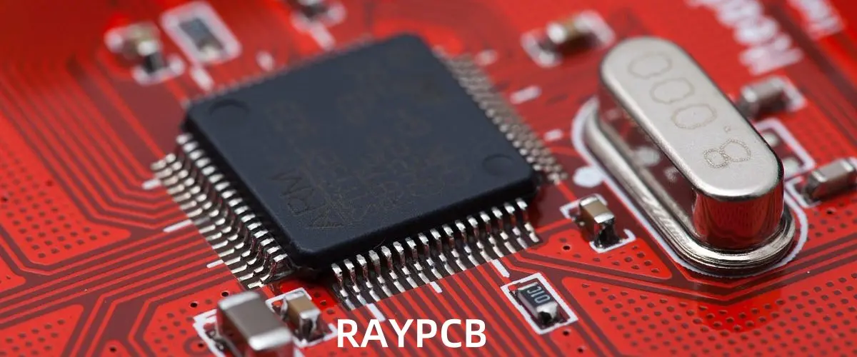
Microcontroller PCBs (Printed Circuit Boards) are the backbone of modern embedded systems. These specialized boards house microcontrollers – small computers on a single integrated circuit – along with necessary supporting components. The importance of custom PCB design in the realm of embedded systems cannot be overstated. A well-designed microcontroller PCB ensures optimal performance, reliability, and efficiency in your electronic projects.
As technology advances and devices become smaller and more complex, the demand for expertly designed microcontroller PCBs continues to grow. Whether you’re working on a smart home device, a wearable health monitor, or an industrial control system, mastering the art of microcontroller PCB design is crucial for success in the field of embedded systems.
II. Step 1: Define Your Project Requirements

Before diving into the schematic design, it’s essential to clearly define your project requirements. This crucial first step will guide all subsequent decisions in your microcontroller PCB design process.
Choosing the Right Microcontroller
Selecting the appropriate microcontroller is fundamental to your project’s success. Consider the following factors:
- Processing power: Decide between 8-bit, 16-bit, or 32-bit microcontrollers based on your application’s computational needs.
- Memory requirements: Evaluate the amount of flash memory and RAM your project requires.
- Peripheral support: Ensure the microcontroller supports the necessary interfaces and peripherals for your application.
- Power consumption: Consider battery life and overall power efficiency, especially for portable devices.
- Cost: Balance features with budget constraints, particularly for high-volume production.
Identifying Required Peripherals
List all the peripherals your project needs. Common peripherals include:
- Analog-to-Digital Converters (ADC) for sensor inputs
- Universal Asynchronous Receiver/Transmitter (UART) for serial communication
- Inter-Integrated Circuit (I2C) and Serial Peripheral Interface (SPI) for interfacing with other devices
- General Purpose Input/Output (GPIO) pins for basic digital interfacing
- Timers and Pulse Width Modulation (PWM) modules for precise timing and control
Defining Power Supply Requirements
Determine the power needs of your microcontroller and all other components on the board:
- Voltage levels: Typically 3.3V or 5V for most microcontrollers, but some components may require different voltages.
- Current draw: Calculate the maximum current consumption of all components.
- Power source: Decide between battery power, USB power, or mains power with appropriate regulation.
- Efficiency: Consider using low-dropout (LDO) regulators or switching regulators for better power efficiency.
Board Dimensions and Enclosure Constraints
Factor in any size limitations or form factor requirements:
- Overall PCB dimensions
- Component height restrictions
- Mounting hole positions
- Connector placements for external interfaces
By thoroughly defining these requirements, you set a solid foundation for your microcontroller PCB design, ensuring that the final product meets all necessary specifications and performs optimally in its intended application.
III. Step 2: Schematic Design
With your project requirements clearly defined, the next step in designing a microcontroller PCB is creating the schematic. This is where you’ll translate your conceptual design into a detailed electronic diagram.
Choosing EDA Tools
Selecting the right Electronic Design Automation (EDA) tool is crucial for efficient schematic design. Popular options include:
- KiCad: Open-source and feature-rich, suitable for beginners and professionals alike.
- Eagle: Known for its extensive component libraries and user-friendly interface.
- Altium Designer: A professional-grade tool with advanced features for complex designs.
- Autodesk Fusion 360 (Electronics): Integrates PCB design with 3D modeling capabilities.
Choose a tool that matches your skill level and project complexity. Many offer free versions or trials, allowing you to experiment before committing.
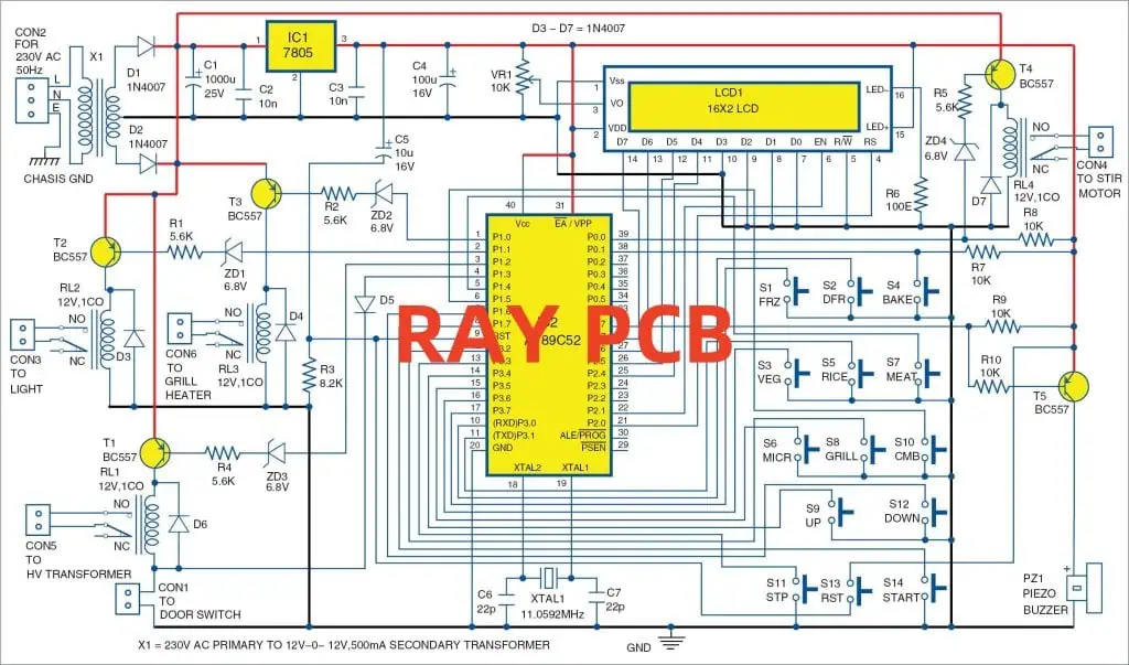
Drawing the Microcontroller Circuit Schematic
When creating your schematic, focus on these key areas:
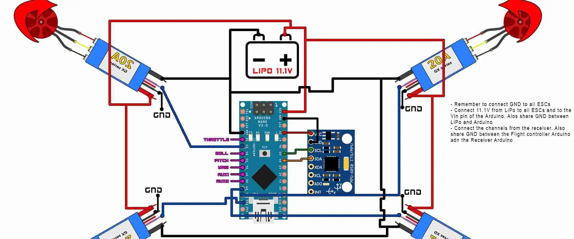
Microcontroller Core Connections
- Power pins: Connect VCC and GND pins to appropriate power planes.
- Decoupling capacitors: Place 0.1μF ceramic capacitors close to each power pin.
- Reset circuitry: Include a reset button and pull-up resistor.
- Clock source: Add a crystal oscillator circuit if using an external clock.
Power Supply and Decoupling
- Voltage regulator: Include appropriate linear or switching regulators.
- Bulk capacitors: Add larger electrolytic capacitors (10-100μF) near voltage regulators.
- Ferrite beads: Use these for isolating digital and analog power supplies if necessary.
Crystal Oscillator and Reset Circuitry
- Crystal connections: Follow manufacturer recommendations for load capacitors.
- Reset circuit: Implement a simple RC circuit with a tactile switch for manual reset.
External Interfaces
- Sensors: Add necessary pull-up/pull-down resistors and filtering capacitors.
- Displays: Include level shifters if required (e.g., for LCD interfaces).
- Communication ports: Add protection components like TVS diodes for exposed interfaces.
Best Practices in Schematic Design
- Use clear and consistent naming conventions for components and nets.
- Group related components together for better readability.
- Use hierarchical sheets for complex designs to improve organization.
- Add detailed notes and comments to explain non-obvious design choices.
- Cross-check component footprints with their physical counterparts.
- Perform thorough electrical rule checks (ERC) to catch common errors.
By following these guidelines and paying attention to detail in your schematic design, you’ll create a solid foundation for the PCB layout phase of your microcontroller project.
Read more about:
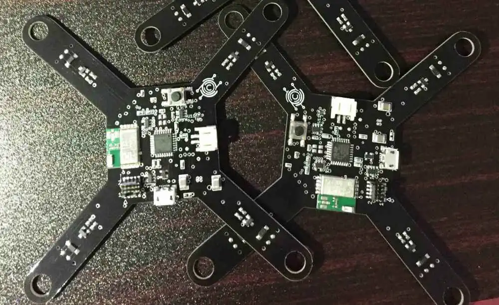
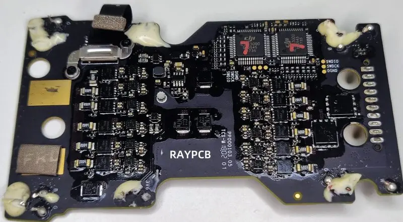
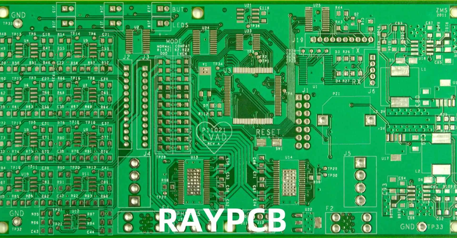
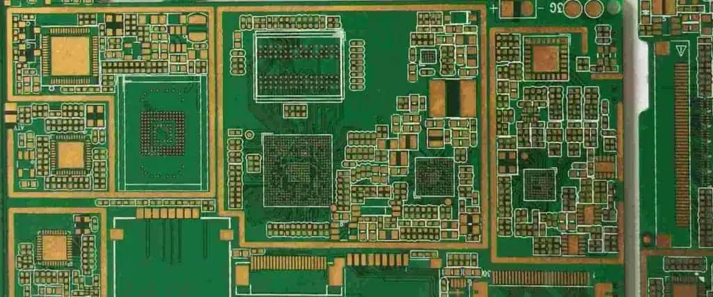
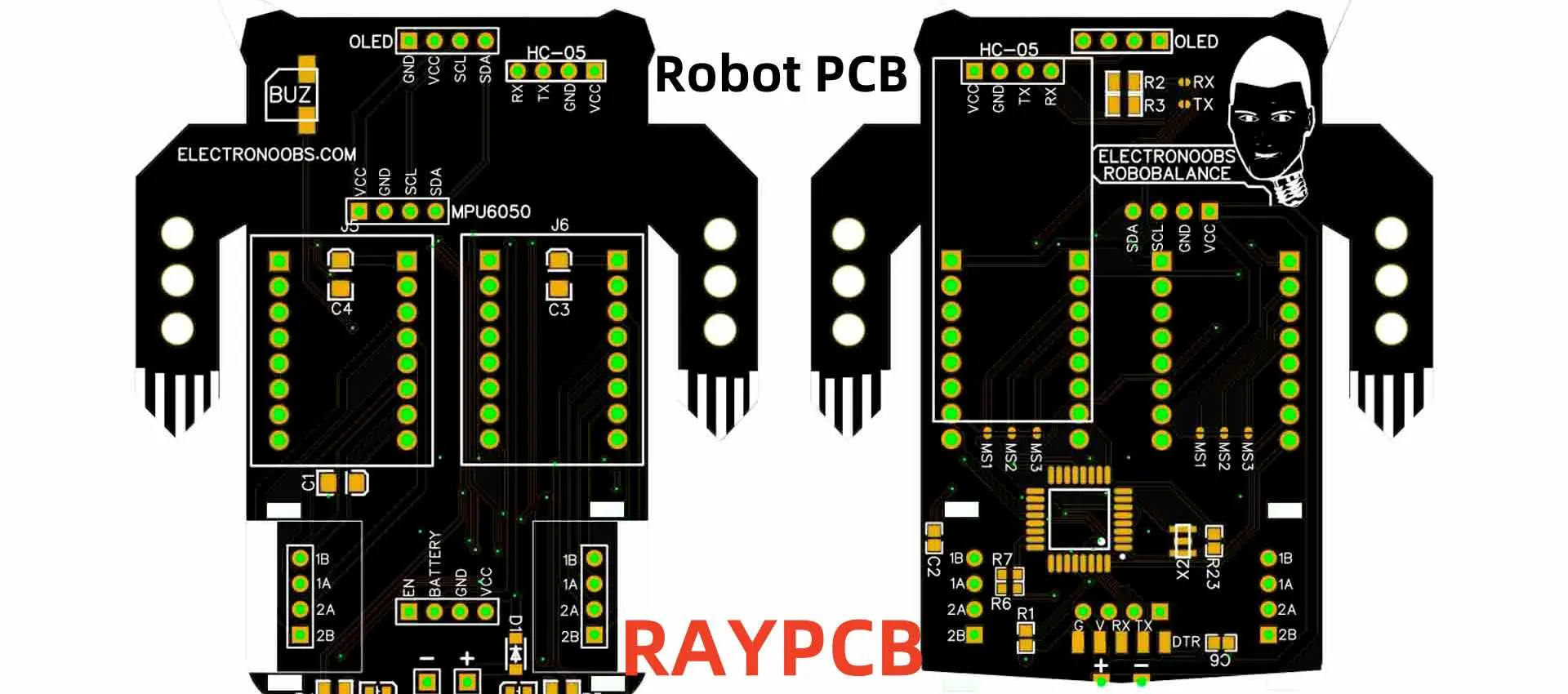
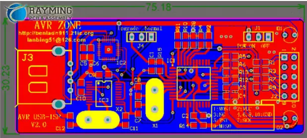
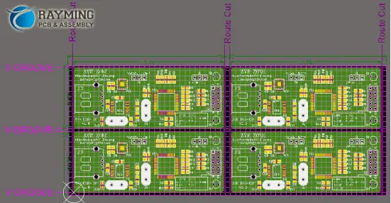
IV. Step 3: PCB Layout
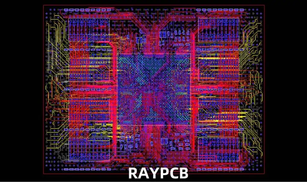
Once your schematic is complete and error-free, it’s time to move on to the PCB layout. This stage transforms your circuit diagram into a physical board design, considering factors like component placement, trace routing, and signal integrity.
Component Placement Strategy
Effective component placement is crucial for a successful microcontroller PCB design:
- Keep the microcontroller central: Place the microcontroller at the heart of your board for optimal connectivity.
- Group related components: Keep functionally related parts close together to minimize trace lengths.
- Consider thermal management: Place heat-generating components away from sensitive parts.
- Optimize for assembly: Align components in a way that simplifies the manufacturing process.
- Plan for test points: Leave space for test points near critical signals for easier debugging.
Routing Guidelines for Microcontroller PCB Layout
Signal Integrity for High-Speed Lines
- Keep high-speed traces short and direct.
- Use differential pairs for high-speed interfaces like USB or Ethernet.
- Avoid right-angle turns in traces; use 45-degree angles or curves instead.
- Consider impedance matching for critical high-frequency signals.
Ground Planes and Power Distribution
- Use a solid ground plane on a dedicated layer when possible.
- Implement star grounding for analog and digital grounds if necessary.
- Use wide traces or copper pours for power distribution.
- Place vias near decoupling capacitors to reduce inductance.
Trace Width, Via Usage, and DRC Checks
- Calculate appropriate trace widths based on current requirements.
- Use larger vias for power and ground connections.
- Avoid placing vias in pad unless necessary for high-density designs.
- Run Design Rule Checks (DRC) frequently to catch and correct errors early.
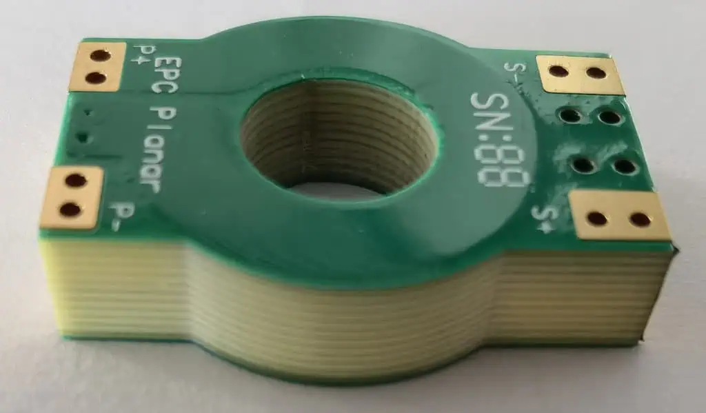
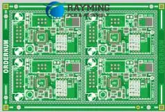
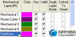
Single-Layer vs. Multi-Layer PCB Design Choices
Consider the trade-offs between single-layer and multi-layer designs:
Single-Layer PCBs
- Pros: Lower cost, simpler manufacturing process.
- Cons: Limited routing options, potential for more noise and interference.
Multi-Layer PCBs
- Pros: Better signal integrity, more compact designs, easier routing.
- Cons: Higher cost, more complex manufacturing process.
For most microcontroller projects, a 4-layer board offers a good balance between cost and performance. A typical 4-layer stackup might include:
- Top layer: Components and signal routing
- Inner layer 1: Ground plane
- Inner layer 2: Power plane
- Bottom layer: Components and signal routing
By carefully considering these layout guidelines and making informed decisions about layer count, you’ll be well on your way to creating a high-quality microcontroller PCB design.
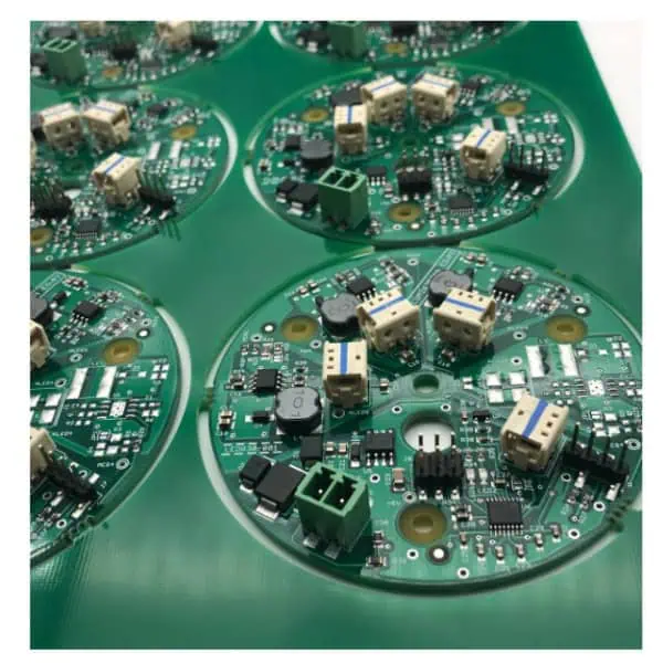
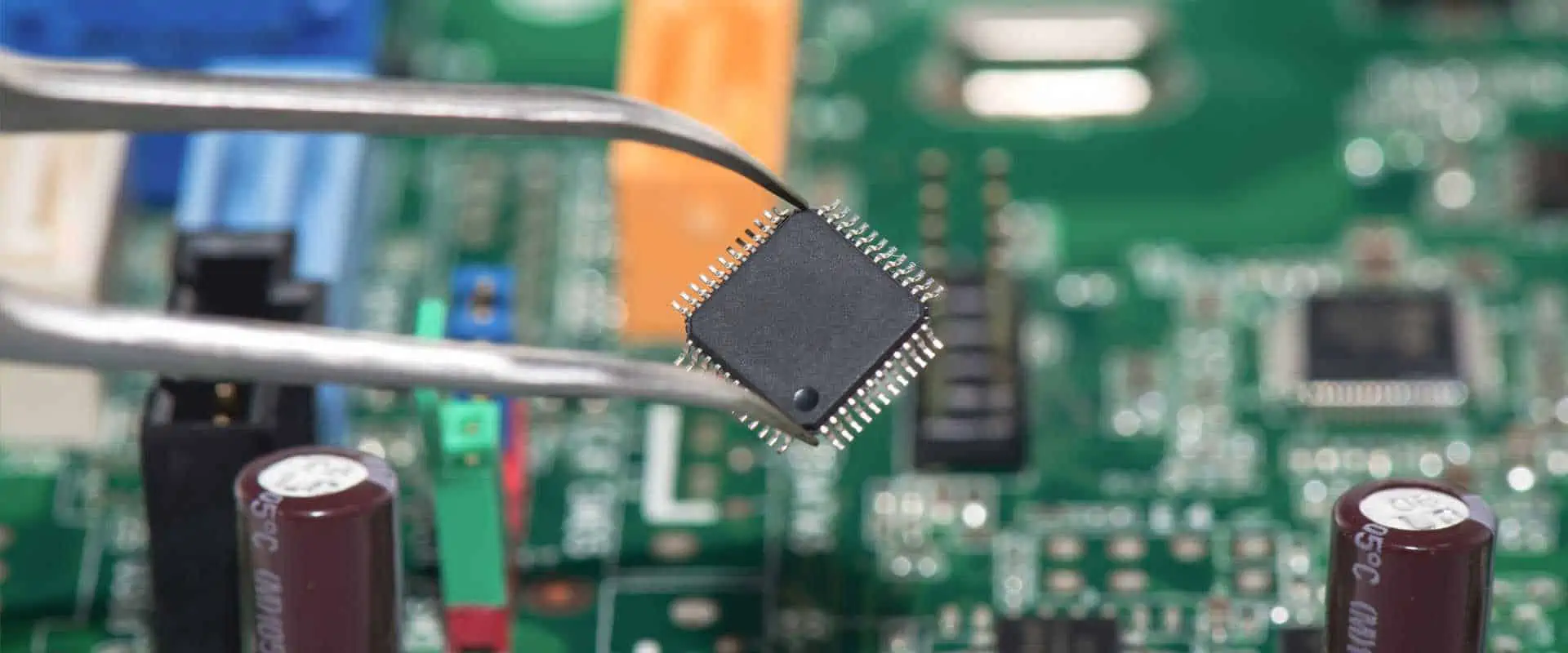
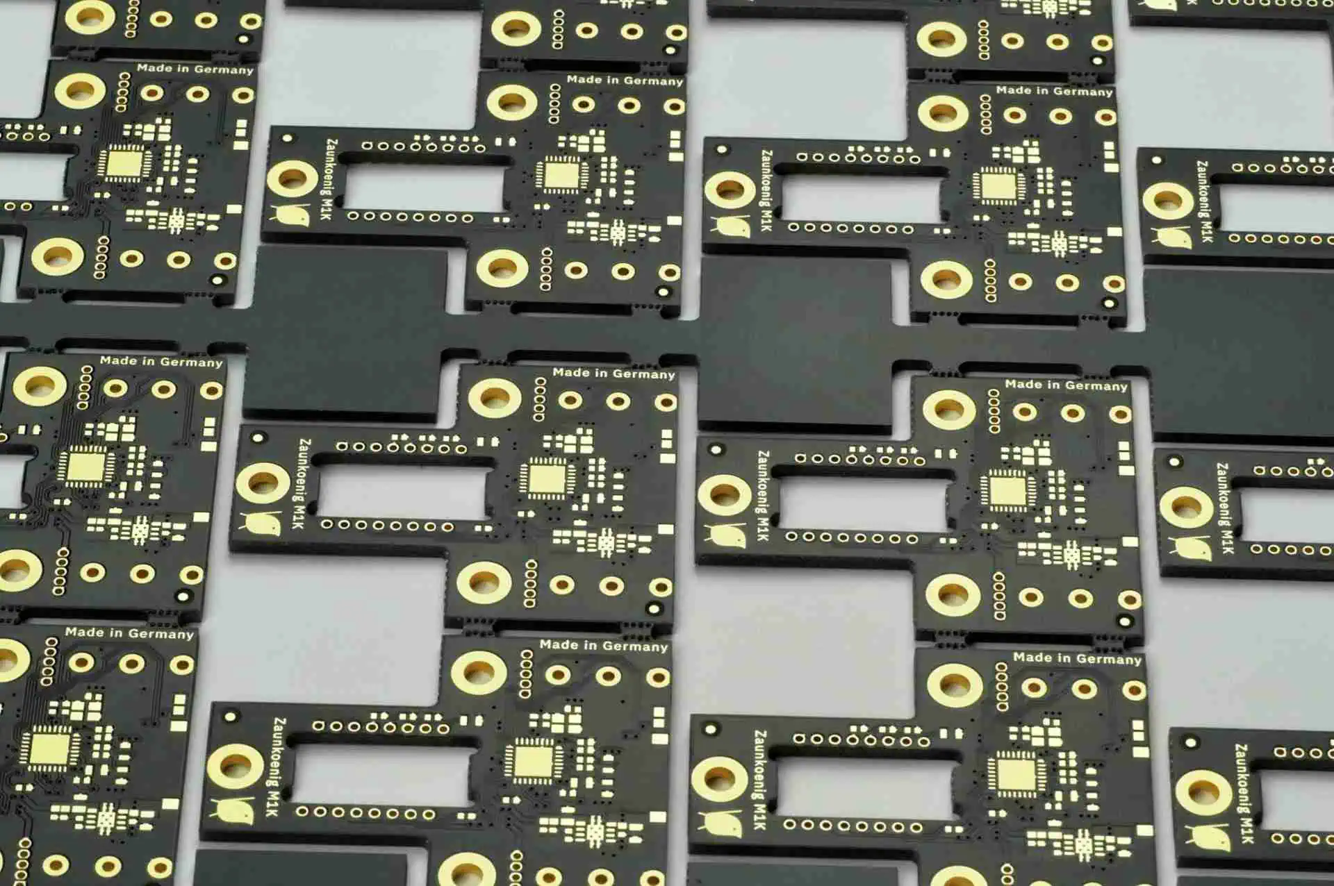
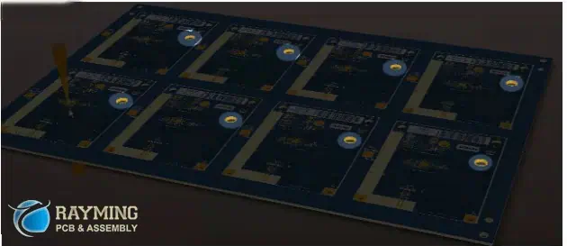
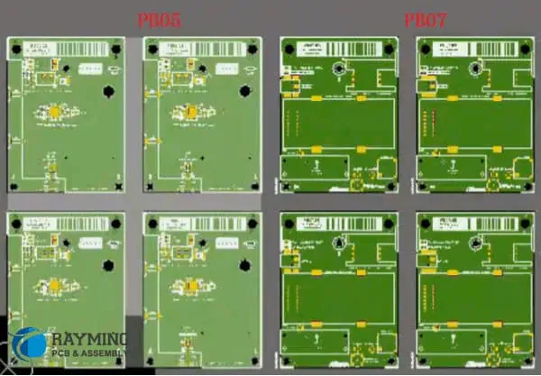
V. Step 4: PCB Prototyping
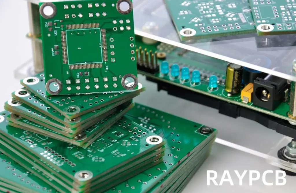
After completing your PCB layout, the next exciting phase is bringing your design to life through prototyping. This stage allows you to validate your design and make necessary adjustments before moving to full-scale production.
Generating Gerber Files and BOM
- Gerber file generation:
- Use your EDA tool to export Gerber files, which contain all the necessary information for PCB fabrication.
- Include files for all copper layers, solder mask, silkscreen, and drill holes.
- Double-check that all layers are correctly aligned and scaled.
- Creating a Bill of Materials (BOM):
- List all components, including their values, packages, and quantities.
- Include manufacturer part numbers and potential alternative parts.
- Organize the BOM in a clear, spreadsheet format for easy reference.
Choosing PCB Fabrication Services
For prototype runs or small batches, consider these factors when selecting a PCB manufacturer:
- Minimum order quantity: Some services offer as few as 3-5 boards for prototyping.
- Turnaround time: Look for services offering quick turnaround for faster iteration.
- Board specifications: Ensure the manufacturer can handle your design’s layer count, minimum trace width, and hole sizes.
- Quality and reliability: Read reviews and check for certifications like ISO 9001.
- Additional services: Some fabricators offer assembly services, which can be convenient for prototyping.
Popular PCB prototype services include:
- PCBWay
- JLCPCB
- OSH Park
- Seeed Studio
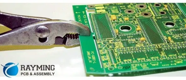
Assembly Tips
Decide between manual soldering and reflow soldering based on your design complexity and component types:
Manual Soldering
- Ideal for through-hole components and simple designs.
- Use a temperature-controlled soldering iron and appropriate flux.
- Start with larger components and work your way to smaller ones.
- Consider using a magnifying glass or microscope for fine-pitch components.
Reflow Soldering
- Better for designs with many surface-mount components.
- Apply solder paste using a stencil or syringe.
- Place components using tweezers or a pick-and-place machine.
- Use a reflow oven or hot air station to melt the solder paste.
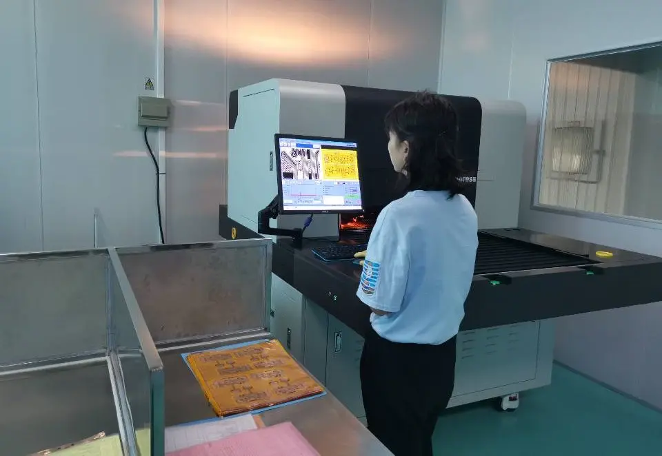
Initial Testing of the Prototype
Before powering up your board:
- Perform a visual inspection for any obvious defects or solder bridges.
- Use a multimeter to check for shorts between power and ground.
- Verify continuity on critical nets and power connections.
When powering up for the first time:
- Use a current-limited power supply to prevent damage from potential shorts.
- Monitor power consumption to ensure it’s within expected ranges.
- Check for expected voltage levels at key test points.
By carefully managing the prototyping process, you can quickly identify and resolve any issues in your microcontroller PCB design, setting the stage for successful programming and comprehensive testing.
VI. Step 5: Programming and Testing
With your microcontroller PCB prototype assembled, it’s time to bring it to life through programming and conduct thorough testing to ensure it meets all your project requirements.
Uploading Code to Your Microcontroller PCB
The method for uploading code depends on your microcontroller and chosen programming interface. Common options include:
- In-System Programming (ISP):
- Use programmers like PICkit for PIC microcontrollers, USBasp for AVR, or ST-Link for STM32.
- Ensure your PCB has the necessary programming header pins.
- JTAG or SWD Interfaces:
- Popular for debugging ARM-based microcontrollers.
- Requires specific pins on the microcontroller to be accessible.
- Bootloaders:
- Allow programming over standard interfaces like UART or USB.
- Require initial bootloader programming but simplify subsequent updates.
Tips for successful programming:
- Double-check connections between the programmer and your board.
- Verify that your programming software recognizes the microcontroller.
- Start with a simple “blink LED” program to confirm basic functionality.
Functional Testing and Debugging
Systematic testing is crucial to verify that your microcontroller PCB functions as intended:
- Power supply testing:
- Verify voltage levels at various test points.
- Check for voltage stability under different load conditions.
- Peripheral testing:
- Test each GPIO pin for input and output functionality.
- Verify analog inputs with known voltage sources.
- Test communication interfaces (UART, I2C, SPI) with loopback tests or external devices.
- Sensor integration:
- Calibrate and test any onboard sensors.
- Verify sensor data acquisition and processing.
- System-level testing:
- Run your full application code and observe overall system behavior.
- Test for edge cases and potential failure modes.
Common Testing Tools
Equip yourself with these essential tools for effective microcontroller PCB testing:
- Multimeter:
- Use for continuity testing, voltage measurements, and current draw analysis.
- Oscilloscope:
- Essential for analyzing signal integrity, timing issues, and communication protocols.
- Look for at least 50MHz bandwidth for most microcontroller applications.
- Logic Analyzer:
- Useful for debugging multi-wire interfaces and complex timing issues.
- Software-based options like Saleae provide affordable solutions for many projects.
- Power Supply:
- A variable, current-limited power supply is invaluable for safe testing.
- Environmental Chamber (optional):
- For testing your PCB under various temperature conditions, if applicable to your project.
By methodically programming and testing your microcontroller PCB, you can identify and resolve issues early, ensuring a robust and reliable final product. Remember to document your testing process and results thoroughly, as this information will be valuable for future iterations and troubleshooting.
VII. Optimization and Final Design Tips
After initial testing, you may find areas where your microcontroller PCB design can be improved. This optimization phase is crucial for enhancing performance, reliability, and manufacturability.
EMC and Noise Reduction Practices
Electromagnetic Compatibility (EMC) is crucial for ensuring your device operates correctly in its intended environment and doesn’t interfere with other electronics:
- Proper grounding:
- Implement a solid ground plane.
- Use star grounding for analog and digital sections if necessary.
- Signal routing:
- Keep high-speed signals away from sensitive analog circuits.
- Use guard traces for isolating noisy signals.
- Filtering:
- Add ferrite beads on power lines to suppress high-frequency noise.
- Use bypass capacitors near ICs to reduce noise on power rails.
- Shielding:
- Consider adding a shield can for sensitive RF circuits or in noisy environments.
Thermal Management Considerations
Proper thermal management ensures your microcontroller and other components operate within their specified temperature ranges:
- Component placement:
- Keep heat-generating components away from temperature-sensitive parts.
- Use thermal vias under hot components to help dissipate heat.
- Copper pours:
- Increase copper area for better heat dissipation.
- Use thermal relief patterns to balance heat dissipation and solderability.
- Forced air cooling:
- Consider adding spaces for fans or heat sinks if natural convection is insufficient.
Design for Manufacturability (DFM) and Testability (DFT)
Optimizing your design for manufacturing and testing can save time and reduce costs:
- Component selection:
- Use commonly available parts to avoid supply chain issues.
- Consider using parts with multiple sources.
- Board layout:
- Maintain consistent component orientation for easier assembly.
- Leave adequate space between components for pick-and-place machines.
- Testability:
- Add test points for critical signals.
- Excellent for both beginners and professionals.
- Extensive library of components and active community support.
- Fusion 360 Electronics:
- Combines electrical and mechanical design in one platform.
- Great for projects requiring integrated enclosure design.
5. CircuitMaker:
- Free, community-driven PCB design tool by Altium.
- Good for collaborative projects and open-source hardware.
Free Libraries and Reference Designs
- SnapEDA:
- Extensive library of PCB footprints and symbols.
- Integration with multiple PCB design software.
- Ultra Librarian:
- Large collection of pre-made component models.
- Supports various EDA tools.
- Microcontroller Manufacturer Resources:
- ST Microelectronics, Microchip, and Texas Instruments offer reference designs and development board schematics.
- Valuable for understanding best practices and typical implementations.
- OpenCores:
- Open-source hardware designs, including microcontroller-based projects.
- Useful for learning from real-world implementations.
Online Communities for PCB Design and Embedded Systems
- EEVblog Forum:
- Active community discussing electronics design and PCB layout.
- Valuable for troubleshooting and getting expert advice.
- Reddit Communities:
- r/PrintedCircuitBoard for PCB design discussions.
- r/embedded for embedded systems and firmware development.
- Stack Exchange:
- Electrical Engineering Stack Exchange for technical questions.
- Arduino Stack Exchange for microcontroller programming queries.
- Hackster.io:
- Platform for sharing and discovering hardware projects.
- Offers tutorials and project ideas for microcontroller applications.
- element14 Community:
- Forums, blogs, and webinars on electronics design.
- Hosts design challenges and provides access to technical resources.
By leveraging these tools and resources, you can enhance your skills, stay updated with the latest trends, and connect with fellow enthusiasts in the field of microcontroller PCB design.
X. Conclusion
Mastering the art of microcontroller PCB design is a journey that combines technical knowledge, creativity, and practical experience. As we’ve explored throughout this guide, the process involves several key steps:
- Defining project requirements
- Creating a detailed schematic
- Developing an efficient PCB layout
- Prototyping and testing
- Optimizing for performance and manufacturability
Each of these stages is crucial in creating a successful microcontroller PCB that meets your project’s needs and performs reliably in real-world conditions.
The importance of this skill cannot be overstated in today’s technology-driven world. From IoT devices and industrial automation to consumer electronics and cutting-edge robotics, microcontroller PCBs are at the heart of countless innovations. By honing your ability to design these boards effectively, you open doors to faster innovation and more efficient product development.
Remember that PCB design is both an art and a science. While following best practices and guidelines is important, there’s also room for creative problem-solving and innovative approaches. Each project brings its own unique challenges and opportunities for learning.
We encourage you to take the knowledge gained from this guide and apply it to your own projects. Start with simple designs and gradually tackle more complex challenges. Experiment with different microcontrollers, explore various peripherals, and push the boundaries of what’s possible within the constraints of PCB design.
Keep in mind that the field of electronics is ever-evolving. Stay curious, keep learning, and don’t hesitate to engage with the vibrant community of makers, engineers, and hobbyists who share your passion for microcontroller PCB design.
By embracing the iterative process of design, prototyping, and testing, you’ll not only improve your skills but also contribute to the exciting world of embedded systems and IoT. Your next design could be the foundation of a groundbreaking product or the solution to a complex problem.
So, fire up your favorite EDA tool, choose a microcontroller, and start designing. The world of microcontroller PCB design is vast and full of possibilities – your next great project awaits!
XI. FAQ
To address common queries and enhance SEO, here are answers to frequently asked questions about microcontroller PCB design:
What is a microcontroller PCB?
A microcontroller PCB (Printed Circuit Board) is a specialized board designed to house and connect a microcontroller along with its supporting components. It serves as the physical foundation for embedded systems, integrating the microcontroller with various peripherals, power supply circuitry, and interfaces needed for the specific application.
How do I design a PCB for a microcontroller?
Designing a PCB for a microcontroller involves several steps:
- Define your project requirements and choose an appropriate microcontroller.
- Create a schematic diagram of your circuit using EDA software.
- Develop the PCB layout, carefully placing components and routing traces.
- Generate manufacturing files (Gerbers) and order a prototype.
- Assemble and test your PCB, making iterations as necessary.
Which software is best for microcontroller circuit design?
The best software depends on your specific needs and experience level. Popular options include:
- KiCad: Free, open-source, and feature-rich.
- Altium Designer: Professional-grade with advanced features.
- Eagle: User-friendly with a large component library.
- Fusion 360 Electronics: Integrates electrical and mechanical design.
Choose software that aligns with your project complexity and budget.
How do you test a microcontroller board?
Testing a microcontroller board involves several stages:
- Visual inspection for manufacturing defects.
- Continuity testing of power and critical signal paths.
- Power-on testing with a current-limited supply.
- Functional testing of individual peripherals and interfaces.
- Uploading and running test firmware to verify overall functionality.
- Stress testing under various operating conditions.
Use tools like multimeters, oscilloscopes, and logic analyzers for comprehensive testing.
What are the common mistakes in PCB layout?
Common PCB layout mistakes include:
- Inadequate clearance between components or traces.
- Poor power distribution and insufficient decoupling.
- Ignoring signal integrity for high-speed lines.
- Improper grounding techniques.
- Neglecting thermal considerations for heat-generating components.
- Failing to include test points for debugging.
- Overlooking manufacturing constraints and design for assembly.
Avoid these pitfalls by following best practices and thoroughly reviewing your design before fabrication.