The ESP32, a powerful and versatile microcontroller, has become a cornerstone in the world of Internet of Things (IoT), embedded systems, and DIY projects. Its popularity stems from its robust Wi-Fi and Bluetooth capabilities, coupled with an impressive array of peripherals and processing power. However, to fully harness the potential of this remarkable chip, proper ESP32 PCB design is crucial.
In this comprehensive guide, we’ll delve into the best practices for ESP32 PCB design, focusing on power management, layout techniques, and ensuring signal integrity. Whether you’re using popular design tools like EasyEDA for ESP32 or Altium Designer for ESP32, these principles will help you create more efficient, reliable, and high-performing ESP32-based devices.
Pay special attention to clearance and isolation rules for RF sections
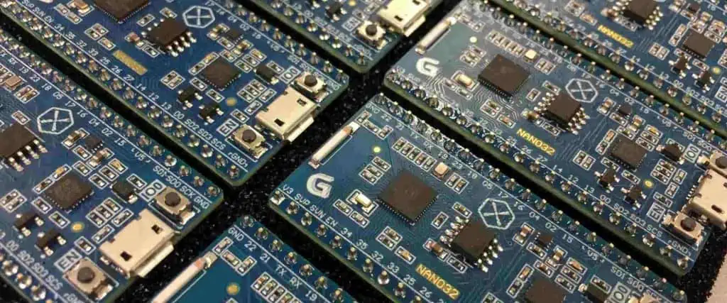
Prototyping with Small Batch PCB Services
Consider using rapid prototyping services for initial testing
Evaluate multiple vendors for quality and turnaround time
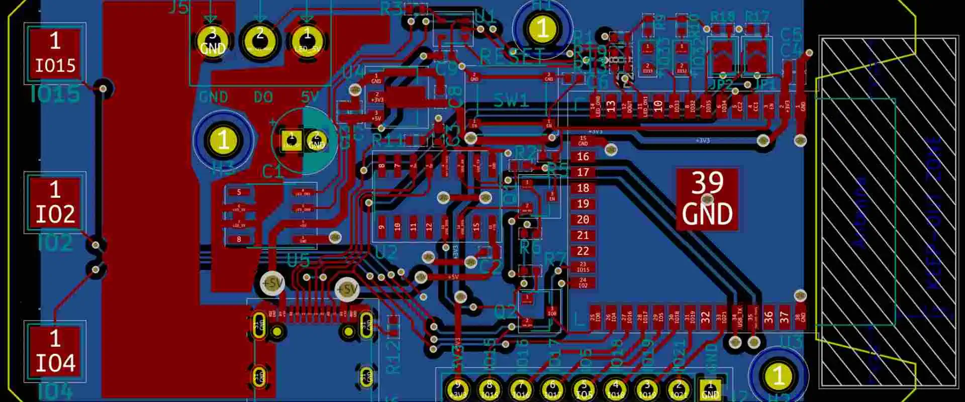
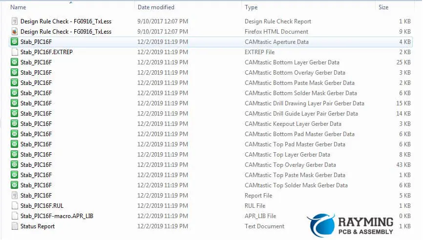
Preparing Gerber Files for ESP32 PCB Manufacturing
Generate a complete set of Gerber files, including drill files
Double-check layer stackup and board outline
Conclusion
Mastering ESP32 PCB design is a journey that combines understanding the intricacies of the ESP32 hardware with applying solid PCB design principles. By focusing on power design, layout techniques, and signal integrity, you can create ESP32-based projects that are not only functional but also reliable and efficient.
Remember that tools like EasyEDA and Altium Designer for ESP32 can significantly streamline your design process, but the underlying principles remain the same. As you continue to work with ESP32 PCB design, you’ll develop an intuition for what works best in different scenarios.
Keep iterating on your designs, stay updated with the latest ESP32 developments, and don’t hesitate to experiment with new techniques. With practice and attention to detail, you’ll soon be creating professional-grade ESP32 PCBs that stand out in performance and reliability.
FAQ
What is the best PCB design software for ESP32?
The best PCB design software for ESP32 depends on your needs and experience level. For beginners and hobbyists, EasyEDA offers a user-friendly interface and is sufficient for many ESP32 projects. For professional designers working on complex ESP32 boards, Altium Designer provides advanced features and greater control over the design process.
How to improve signal integrity in ESP32 PCB layout?
To improve signal integrity in ESP32 PCB layout:
Use a solid ground plane
Keep high-speed traces short and direct
Implement proper decoupling
Use controlled impedance for critical traces
Pay attention to return paths for high-speed signals
Can I design ESP32 boards with EasyEDA?
Yes, you can design ESP32 boards with EasyEDA. It offers a library of ESP32 components and modules, making it easy to create schematics and PCB layouts for ESP32-based projects. While it may lack some advanced features found in professional tools, EasyEDA is capable of producing high-quality ESP32 PCB designs for many applications.
What are common mistakes in ESP32 board design?
Common mistakes in ESP32 board design include:
Inadequate power decoupling
Poor RF layout and antenna design
Improper grounding techniques
Overlooking thermal management
Ignoring signal integrity for high-speed interfaces
Failing to consider EMI/EMC requirements
By being aware of these potential pitfalls and following best practices, you can avoid many common issues in ESP32 PCB design.
Learn how to design professional KiCad flex PCB projects using only open-source tools. This comprehensive guide will walk you through everything you need to know about creating flexible printed circuit boards with KiCad, from basic concepts to advanced techniques.
Understanding Flex PCBs
Flexible printed circuit boards (flex PCBs) represent a revolutionary advancement in electronics design, offering capabilities that traditional rigid boards simply cannot match. These bendable, lightweight circuit platforms are transforming industries from consumer electronics to medical devices.
What is a Flexible PCB?
A flexible PCB is a circuit board manufactured on a flexible substrate, typically polyimide, that allows the board to bend, fold, and conform to three-dimensional shapes. Unlike their rigid counterparts, flex PCBs can be twisted, curved, and even dynamically flexed during operation, opening up new possibilities for electronic design.
Common Applications for Flex Circuits
Flex PCB technology has found its way into numerous applications:
Consumer electronics: Smartphones, tablets, and wearables
Medical devices: Hearing aids, pacemakers, and implantable sensors
Automotive electronics: Dashboard displays and control systems
Aerospace: Satellite components and lightweight avionics
Industrial equipment: Rotating and moving assemblies
Differences Between Flex, Rigid, and Rigid-Flex PCBs
Understanding the distinctions between these PCB types is crucial for effective design:
Flex PCBs: Completely flexible, can bend in multiple directions, ideal for dynamic applications
Rigid PCBs: Traditional solid circuit boards with no flexibility
Rigid-Flex PCBs: Hybrid designs combining rigid sections for components with flexible interconnections
Key Challenges in Flex PCB Design
Designing flex PCBs comes with unique considerations:
Managing bend radii to prevent copper trace fractures
Accounting for material elongation and compression during flexing
Ensuring reliable connections between components and the flexible substrate
Controlling impedance across bending areas
Optimizing layer stackups for both flexibility and functionality
KiCad flex PCB design is now easier than ever thanks to recent software advancements in this powerful open-source EDA (Electronic Design Automation) suite. More designers are turning to KiCad for their flexible circuit needs.
The Open-Source Advantage
KiCad’s open-source nature provides several distinct benefits:
Zero licensing costs: Completely free for personal and commercial use
Full feature set: Access to professional-grade PCB design capabilities
Transparency: Direct visibility into how the software functions
Customizability: Ability to modify the software for specific requirements
Cost Savings vs. Proprietary Tools
When compared to commercial alternatives like Altium Designer or Cadence Allegro, KiCad offers substantial savings:
No recurring subscription fees (saving thousands annually)
No seat licensing restrictions for team environments
Free updates and new feature releases
Reduced training costs through accessible documentation
Community Support and Available Plugins
The vibrant KiCad community provides valuable resources:
Pro Tip: How to set up your first KiCad flex PCB project correctly
For best results, start by creating custom design rule profiles specifically for flexible circuits. Set up separate rules for rigid areas and flexible zones, with more conservative constraints for the latter. This dual-rule approach helps prevent common flex PCB failures.
Schematic Capture for Flex PCBs
Effective schematic design is the foundation of successful flex PCBs.
Tips for Modular, Flexible Designs
Create schematics with flexibility in mind:
Organize circuits by functional blocks
Use hierarchical sheets for complex designs
Consider physical layout requirements during schematic design
Group components that will reside on the same flex section
Net Naming Conventions for Complex Circuits
Implement clear naming standards:
Use descriptive prefixes for different flex sections
Label critical signals that cross bend areas
Document high-speed signals requiring impedance control
Create naming hierarchies for complex multi-board designs
Best Practices for Schematic Clarity
Enhance readability and maintainability:
Add detailed annotations about flex requirements
Include mechanical constraints as drawing notes
Use color coding for different flex regions
Document expected bend locations and requirements
PCB Layout: Flex-Specific Strategies
The layout phase requires specialized techniques for successful flex PCB design.
Setting Board Outlines and Flexible Zones
Define your flex PCB geometry:
Create precise board outlines following mechanical requirements
Designate flex zones with clear boundary markings
Add bend indicators for fabrication guidance
Include alignment features for assembly
Designing for Bending and Dynamic Flexing
Accommodate movement in your design:
Place traces perpendicular to bend lines when possible
Use curved traces rather than right angles in flex areas
Implement teardrop pad transitions for improved durability
Stagger traces across layers to prevent stress concentration
Trace Width and Spacing Recommendations
Follow these guidelines for reliable flex circuits:
Use wider traces in flex regions (minimum 0.15mm recommended)
Maintain greater spacing between traces in bend areas
Avoid abrupt width transitions in flexible sections
Consider using rounded corners for all traces
Via and Pad Design Considerations
Optimize these critical elements:
Eliminate vias in flex regions when possible
Use larger pads with teardrops for component mounting
Consider anchoring techniques for SMT components
Implement stress relief patterns around pad connections
Adding Stiffeners and Support Regions
Incorporate mechanical reinforcements:
Design stiffener areas for component mounting
Add support for connectors and high-stress regions
Include proper transitions between stiff and flexible areas
Document stiffener materials and thicknesses
Visualizing Bending Areas in KiCad
Enhance your design visibility:
Use separate layers to mark bend lines
Create 3D models showing the expected flex configuration
Add bend radius indicators to fabrication drawings
Include notes about maximum bend angles
Optimizing Copper Pours for Flexibility
Modify standard pour techniques:
Use hatched ground planes instead of solid copper in flex areas
Implement spokes or mesh patterns for improved flexibility
Add strain relief cutouts in copper areas crossing bend regions
Maintain symmetrical copper distribution when possible
Advanced Techniques
Take your KiCad flex PCB designs to the next level with these specialized approaches.
Designing Rigid-Flex Circuits in KiCad
Create hybrid designs:
Define distinct rigid and flexible zones
Implement proper transitions between regions
Use specialized stackups for different areas
Document fabrication requirements precisely
Multi-Board Projects and Panelization Tips
Efficiently produce multiple designs:
Create panelized layouts for cost-effective manufacturing
Include test coupons for quality verification
Add tooling holes and fiducial markers
Design break-away tabs or mouse bites for separation
Include stack-up specifications and material requirements
Add bend line indicators and flex zone markings
Specific Fabrication Notes for Flex Boards
Provide clear manufacturing guidance:
Specify coverlay materials and thicknesses
Document stiffener requirements and locations
Include detailed information on bend requirements
Add notes about dynamic vs. static flex applications
Recommended Fab Houses for Flex PCBs
Consider these manufacturing partners:
PCBWay
JLCPCB
FPCBA
All Flex
MKS Flex
Using KiCad’s Fabrication Outputs Efficiently
Maximize manufacturing success:
Generate comprehensive drill files
Export detailed assembly drawings
Create pick-and-place files for automated assembly
Provide 3D models showing the intended flex configuration
Testing and Validation
Ensure your flex PCB designs perform as expected.
Visual Inspections Specific to Flex PCBs
Look for these critical factors:
Examine bend areas for defects or stress indicators
Check layer alignment in multi-layer designs
Inspect coverlay adhesion and edge coverage
Verify stiffener placement and attachment
Flex Cycle Testing Tips
Validate durability:
Implement systematic bend testing procedures
Document cycle count expectations
Test under environmental extremes when applicable
Monitor for early failure indicators
Common Issues and Prevention
Address these frequent problems proactively:
Trace cracking in bend areas
Delamination of copper from substrate
Component or solder joint failure during flexing
Coverlay separation or adhesion problems
Resources and Further Learning
Continue developing your KiCad flex PCB design skills.
Useful KiCad Plugins and Scripts
Enhance your workflow with these tools:
KiCad StepUp for improved mechanical integration
InteractiveHtmlBom for assembly documentation
KiCost for bill of materials management
RF-tools-KiCad for impedance calculations
Links to Official Documentation
Access authoritative information:
KiCad official documentation (docs.kicad.org)
IPC-2223 Sectional Design Standard for Flexible PCBs
Material manufacturer design guidelines
Fabrication house design rules
Recommended Forums and Communities
Connect with fellow designers:
KiCad.info Forums
Reddit’s r/KiCad and r/PrintedCircuitBoard
EEVblog Electronics Forum
PCB Design Stack Exchange
Conclusion
With practice, anyone can master KiCad flex PCB design and create professional flexible circuits. The combination of powerful open-source tools and a supportive community makes KiCad an excellent choice for flex PCB development. As flexible electronics continue to grow in importance across industries, the skills you develop using KiCad for flex design will become increasingly valuable.
By following the guidelines in this article, you’ll be well-equipped to tackle flex PCB projects of varying complexity. Remember that successful flex PCB design requires attention to both electrical and mechanical considerations, with particular focus on materials, bend requirements, and manufacturing constraints.
We encourage you to experiment with KiCad’s flex PCB capabilities and share your experiences with the open-source community. Each project contributes to the collective knowledge base and helps advance the state of flexible circuit design for everyone.
Frequently Asked Questions
What minimum trace width should I use for flex PCB designs in KiCad?
For flexible circuits, it’s recommended to use trace widths of at least 0.15mm (6 mil) in bend areas. This provides better durability during flexing compared to narrower traces. For static areas, standard trace widths can be used, but always verify your manufacturer’s capabilities first.
Can KiCad handle rigid-flex PCB designs?
Yes, KiCad can handle rigid-flex PCB designs through careful layer stack-up configuration and zone management. The process requires defining different design rules for rigid and flex sections, creating appropriate board outlines, and adding detailed fabrication notes. Recent versions of KiCad have improved support for these hybrid designs.
How do I indicate bend lines in KiCad for flex PCB manufacturing?
The best practice is to create dedicated layers for bend lines using KiCad’s user layers. These should be included in your fabrication outputs with clear annotations about bend direction, radius, and whether the bend is dynamic or static. Adding dimensioned drawings showing the bend specifications is also highly recommended.
What’s the main difference between designing a regular PCB and a flex PCB in KiCad?
The main differences involve mechanical considerations, trace routing approaches, and layer stack-up. Flex PCBs require careful attention to bend areas, typically use fewer layers, need wider traces in flex regions, and often include stiffeners for component mounting. Design rules must be more conservative, and copper pours should use hatched patterns rather than solid fills in bend areas.
How can I test my flex PCB design before manufacturing?
Before committing to fabrication, use KiCad’s 3D viewer to visualize the design, verify all DRC rules are properly configured for flex circuits, perform manual reviews of bend areas, and consider creating simplified mechanical prototypes using paper or plastic films to validate the folding concept. For critical designs, some manufacturers offer prototype services with faster turnarounds specifically for testing flex circuit concepts.
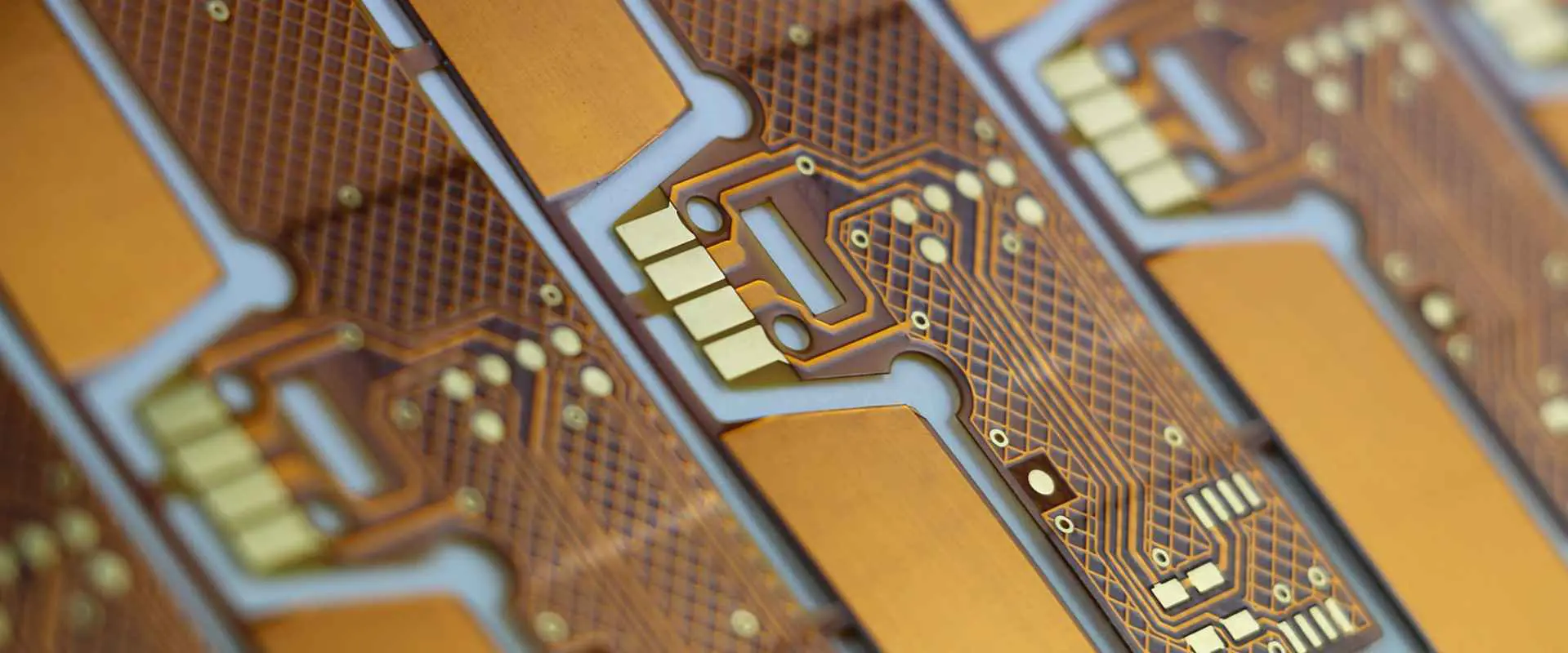
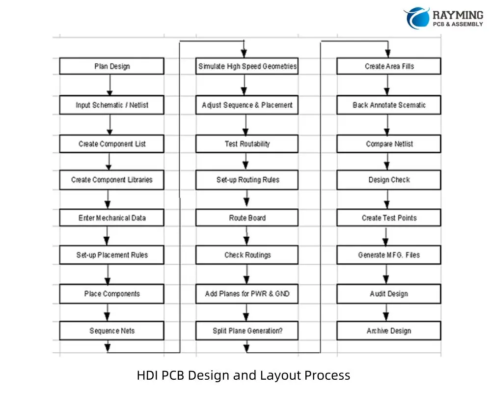
In today’s rapidly evolving electronics landscape, the demand for smaller, faster, and more powerful devices continues to drive innovation in printed circuit board (PCB) technology. High Density Interconnect (HDI) PCB design has emerged as a critical solution to meet these ever-increasing requirements. As electronic devices shrink in size while simultaneously growing in functionality, HDI PCBs have become the backbone of modern electronics manufacturing.
HDI PCB technology enables engineers to pack more components and connections into significantly smaller spaces without compromising performance or reliability. From the smartphone in your pocket to lifesaving medical devices and advanced automotive systems, HDI PCBs are powering the electronics revolution across virtually every industry.
This comprehensive guide explores the fundamental principles, design considerations, and best practices for HDI PCB design. Whether you’re an experienced PCB designer looking to refine your HDI techniques or an engineer exploring high-density solutions for the first time, this article will provide valuable insights to help you optimize your designs for performance, manufacturability, and cost-effectiveness.
High Density Interconnect (HDI) PCBs are advanced printed circuit boards characterized by higher wiring density per unit area than conventional PCBs. This increased density is achieved through finer lines and spaces, smaller vias, and more sophisticated build-up layer structures. The Institute for Printed Circuits (IPC) defines HDI as a PCB with a higher routing density than conventional PCBs, typically featuring:
Microvias with diameters less than or equal to 150 microns
Capture pads with diameters less than or equal to 400 microns
Conductor line width/spacing of 100 microns or less
High connection pad density (>20 pads per square centimeter)
Evolution of HDI Technology
HDI technology represents the natural evolution of PCB design, driven by the miniaturization trends in electronics. While traditional PCBs have served the industry well for decades, they reached practical limitations as component densities increased and signal integrity requirements became more demanding.
The development of laser drilling technology in the 1990s was a pivotal moment for HDI, enabling the creation of much smaller vias than was possible with mechanical drilling. This technological breakthrough, combined with advances in laminate materials and manufacturing processes, paved the way for today’s sophisticated HDI designs.
Importance of HDI Design in Modern Electronics
HDI PCB technology has become indispensable across numerous industries:
Consumer Electronics: Smartphones, tablets, and wearables rely on HDI to achieve their compact form factors while accommodating increasingly powerful processors and more features.
Medical Devices: Implantable and portable medical equipment benefits from the size reduction and reliability improvements HDI offers.
Automotive Electronics: Advanced driver assistance systems (ADAS), infotainment, and vehicle control modules leverage HDI to meet strict space constraints and reliability requirements.
Aerospace and Defense: Mission-critical systems utilize HDI for its superior signal integrity and robustness in harsh environments.
Telecommunications: 5G infrastructure and networking equipment depend on HDI to handle high-frequency signals and thermal challenges.
What Makes an HDI PCB Different from Standard PCBs?
Key Technological Differences
HDI PCBs differ from standard PCBs in several fundamental ways:
Microvias
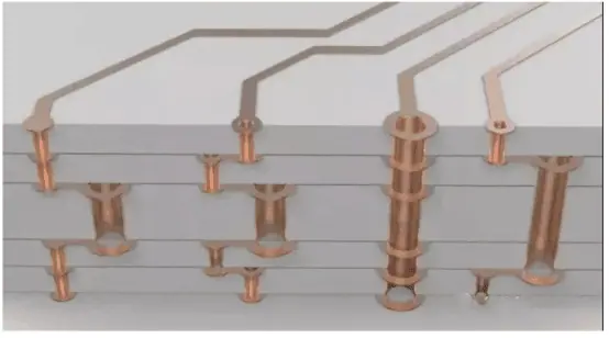
Perhaps the most distinctive feature of HDI technology is the use of microvias—small holes typically less than 150 microns in diameter that create connections between adjacent layers. Unlike conventional through-holes that span the entire board, microvias connect only specific layers, allowing for more efficient use of routing space. These microvias are typically created using laser drilling rather than mechanical methods, enabling much higher precision.
Blind and Buried Vias
HDI designs make extensive use of specialized via structures:
Blind vias: Connect an outer layer to one or more inner layers without passing through the entire board
Buried vias: Connect internal layers without extending to either outer surface
These structures allow designers to create more efficient interconnections while preserving valuable routing space on critical layers.
Finer Lines and Spaces
HDI PCBs feature significantly narrower conductor traces and smaller spacing between them—often 100 microns or less compared to 150-200 microns in standard PCBs. This increased density allows for more signal traces in the same area, supporting higher component densities.
More Complex Layer Stacks
HDI boards typically employ build-up construction methods with multiple lamination cycles, creating sophisticated layer structures that optimize signal routing while minimizing the overall board thickness.
Advantages of HDI PCBs
The technological differences of HDI translate into several significant advantages:
Reduced Size and Weight
The most obvious benefit of HDI is the dramatic reduction in PCB size and weight. By utilizing finer traces, smaller vias, and more efficient routing strategies, HDI designs can achieve the same functionality in a fraction of the space required by conventional PCBs—often reducing board area by 40-60%.
Enhanced Electrical Performance
HDI designs offer superior electrical performance through:
Shorter signal paths that reduce propagation delays
Reduced parasitic inductance and capacitance
Better control of impedance for high-speed signals
Improved power distribution with lower DC resistance
The layer stack is the foundation of any HDI design. Several common approaches exist, each offering different trade-offs between complexity, performance, and cost:
1+N+1 Structure
This basic HDI configuration features a conventional core with one build-up layer on each side. It supports blind vias from outer layers to the adjacent inner layers but does not include buried vias. This approach offers moderate density improvements while keeping manufacturing costs reasonable.
2+N+2 Structure
With two build-up layers on each side of the core, this structure allows for more sophisticated interconnection strategies, including stacked and staggered vias between the build-up layers. This approach provides greater routing density but requires additional lamination cycles.
Any-Layer Structure
The most advanced HDI designs employ “any-layer” technology, where microvias can connect any two adjacent layers throughout the board. This approach offers maximum design flexibility but increases manufacturing complexity and cost.
Via Types and Structures
Understanding via options is crucial for effective HDI design:
Laser-Drilled Microvias
These small-diameter vias (typically 50-150 microns) are formed using laser drilling, which offers greater precision than mechanical methods. Laser drilling is particularly effective for creating blind vias in thin dielectric layers.
Stacked vs. Staggered Vias
Stacked vias: Align directly on top of each other, creating a vertical connection through multiple layers. While space-efficient, stacked vias can create reliability challenges due to stress concentration.
Staggered vias: Offset horizontally from each other, distributing stress more evenly. Though they require more horizontal space, staggered vias generally offer better reliability.
Via-in-Pad
This technique places vias directly within component pads, eliminating the need for fan-out traces and significantly reducing the PCB footprint. Via-in-pad designs require filled and plated-over vias to create a flat surface for component mounting.
Material Considerations
HDI designs impose specific requirements on PCB materials:
High-Tg Laminates
Glass transition temperature (Tg) indicates when a material transitions from rigid to more pliable. HDI PCBs typically utilize high-Tg materials (170°C or higher) to withstand multiple lamination cycles and provide dimensional stability.
Resin-Coated Copper (RCC)
RCC consists of a thin layer of copper foil coated with partially cured resin. It’s commonly used in build-up layers for HDI PCBs because it eliminates the need for copper plating within microvias.
Low-Loss Materials
For high-frequency applications, low-loss dielectric materials such as modified FR-4, PTFE, or ceramic-filled hydrocarbon resins help maintain signal integrity by reducing dielectric losses.
5G requiring materials with extremely low losses at millimeter-wave frequencies
AI accelerators demanding unprecedented power delivery and thermal management
Edge computing necessitating complex mixed-signal designs in compact formats
Automotive electronics requiring HDI solutions that meet rigorous reliability standards
Conclusion
High Density Interconnect PCB technology has transformed electronic product design, enabling the remarkable miniaturization and performance improvements we see in modern devices. By understanding the fundamental principles, design considerations, and best practices outlined in this article, engineers can harness HDI’s capabilities to create more competitive and innovative products.
As with any advanced technology, successful HDI implementation requires balancing multiple factors—technical requirements, manufacturing capabilities, reliability considerations, and cost constraints. Close collaboration with your PCB manufacturer throughout the design process is essential for optimizing this balance.
The HDI landscape continues to evolve rapidly, with new materials, manufacturing processes, and design tools regularly emerging. Staying informed about these developments and continuously refining your HDI design skills will be crucial for addressing tomorrow’s electronic design challenges.
FAQs Section
What are the major advantages of using HDI PCBs?
HDI PCBs offer smaller form factors, higher speed signal performance, and better overall reliability compared to traditional PCBs. They enable more functionality in less space, improved thermal management, and enhanced signal integrity for high-frequency applications.
How do microvias improve HDI PCB performance?
Microvias shorten the path of high-speed signals, reduce parasitic inductance, and enable higher routing density. Their smaller size and more precise placement allow for more efficient interconnections between layers, particularly when routing fine-pitch components.
What is the difference between stacked and staggered vias in HDI design?
Stacked vias align directly over one another, useful for very tight layouts but are more costly and potentially less reliable due to concentrated stress points. Staggered vias are offset from each other, distributing thermal and mechanical stress more evenly while requiring more horizontal space.
How do I choose the right stackup for an HDI board?
The optimal stackup depends on your design’s complexity, signal integrity requirements, component density, and manufacturing capabilities. Begin with the minimum layer count needed, ensure symmetrical construction to prevent warpage, and select appropriate materials for your application’s electrical and thermal requirements.
What factors affect the cost of an HDI PCB?
The primary cost drivers include the number of layers, number of lamination cycles, via structure (stacked vs. staggered), materials used, and manufacturing tolerances. More complex designs with multiple lamination cycles and tighter tolerances will significantly increase costs compared to simpler HDI structures.
Generating the NC Drill Files Based on Different Softwares for PCB Design
Printed circuit boards form the backbones of all electronic equipment and devices. There has been a rise in the circuit’s density and the reducing size trends of the electronic products. This has caused circuit boards to transform into a higher complexity.
Vias or holes, which serve as electrical connections forming between the layers and the corresponding functions that a board will use according to the requirements of the design will not work effectively unless you design or manufacture them suitably.
For any unsuitable manufacturing, you can solve it easily. This is by choosing a top PCB manufacturer for unsuitable design. Also, the solution majorly depends on the engineers who have designed the circuit board. They must create a reliable design file with respect to what the fabricators of the PCB does during manufacturing.
It is a general belief that the generation of the NC drill file has been an issue for most engineers of PCB design. This is why it is necessary to summarize the guidelines of the design board on the software for your PCB design.
NC Drill File is also known as numeric control drill file. This indicates a file that regulates all the information relating to via or hole drilling requirements. These include hole location and size, and tooling size.
It is very necessary for engineers of PCB design to create the NC drill files. This is because you can avoid so much trouble by converting the PCB files into Gerber files or NC drill files.
However, the truth is that some engineers end up sending the PCB files to the PCB manufacturer directly. They fail to convert into Gerber files or NC drill files.
The usual workflow is this. After receiving the files of the PCB design, the board fabricators will have to go ahead and convert them into NC drill files. Then can they continue with the manufacturing. This is because the electronic engineers that work in the PCB fabrication house have a different understanding of PCBs from that of PCB engineers. It is possible that the Gerber file isn’t what the pcb designer was expecting.
Furthermore, during the generation of the Gerber files, some indefinite aspects or issues may result. This is due to differentiations in software version. The best solution is, engineers of the PCB design will have to convert these design files to Gerber files. The NC drill files will also be created, which will all be sent to the PCB manufacturers.
What Does the NC Drill File Format Look Like?
You can generate NC Drill files by using almost all the softwares for PCB design with Excellon as its usual or ordinary format. Excellon was initially a CNC system manufacturer for routers and drillers.
Due to its active role as well as long life in PCB routing and drilling equipment, there is an acceptance and coining of Excellon as some industry standards.
Checking Altium Designer’s main interface, click file, then fabrication outputs, after then, click NC Drill files. Next, go to the dialogue of the NC Drill setup, where you have to specify some options, which include the NC Drill Format, Coordinate positions, Trailing/leading zeros, etc.
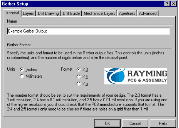
Data units in NC Drill Files could be either millimeters or inches, which should work with those of the Gerber files. As regards the format, there are three major sections present. These include 2:5, 2:4, and 2:3. Here 2:3 shows the least resolution. The 2:5 shows the greatest resolution.
Furthermore, before you go ahead to make a decision regarding the format, it is very important to reach out to the contract manufacturer of the printed circuit board in order to ascertain which of the format works with their level of manufacturing.
With zero suppression, the NC Drill files are driven to be neat and fit and it relies on the application, convenience, and hosts of the PCB designers.
When you suppress leading zeros, the starting zeros will end up being removed. So also, when you pick suppress trailing zeros, then the ending zeros will become removed.
There are two alternatives for coordinate positions. These include relative origin and absolute origin. You should choose any of these according to the specific requirement of the pcb designer. However, it has to be exactly the same as the coordinate positions, which are regulated in the Gerber files.
You can pick other items, if they are necessary for the projects. Once all the items have been determined, just press OK. This generates all the NC Drill files that will be stored into the subfolders default path under the folder that contains the project file.
Generating NC Drill File By Using OrCAD (Cadence Allegro)
This is different from the Altium Designer. The NC Drill Files’ default format that Cadence Allegro exports, is not for Excellon. So, before generating the NC Drill Files for real, it is important to set certain parameters. All you have to do is to click Manufacture, then NC, then NC Parameters. This will help you gain entrance into the NC Parameters dialogue.
In this dialogue, there’s a need to determine the items of Excellon format and Output file. Concerning the Code in the Output file, generally, it is acceptable to pick the ASCII. This is because it is a much newer code type in contrast to EIA.
In order to create an NC Drill File using Excellon’s format, it is important that you click before the Enhanced format of Excellon. To achieve zero suppression, make sure that you click before Trailing or Leading zero suppression with respect to the demands or project needs of the PCB designer or just to conform to the Gerber Files.
Furthermore, after the determination of the items, click the Close button. This will allow the NC Parameters dialogue to escape. After determining the items present in the dialogue, tap Drill. This will end up the generation of the Drill Files generation.
Conclusion
In this article, we have been able to explain ways of generating the NC Drill Files based on different softwares for PCB design. Please message us if you have any questions.
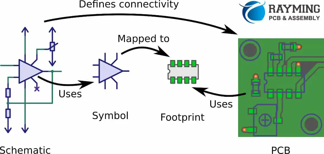
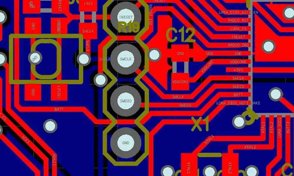
In printed circuit board (PCB) design, the terms “footprint” and “land pattern” are sometimes used interchangeably. However, there are distinct differences between the two. Understanding these subtle differences can help optimize PCB development workflows and avoid mishaps during manufacturing. This article will examine footprints and land patterns in detail, how they complement each other, and best practices for implementation.
Footprints for PCB Assembly
A footprint represents the physical footprint that a component will occupy on the assembled PCB. The footprint provides an outline of the component body and visually indicates how much board space that component consumes.
Key elements of a footprint include:
RefDes – Component reference designator like R1, C112, U3, etc.
Body outline – Rectangular or other shape showing component boundaries
Pin location holes – Placement of pins for through-hole components
Assembly information – Reference text, polarity markings, identifiers
Courtyard – Area that must be kept clear around component
The footprint does not define actual copper pad shapes for connecting to the component. It only provides an abstraction of the component location and space requirements needed for PCB assembly planning.
The land pattern defines the physical pads, traces, and copper features needed to electrically connect to pins or leads on the component. Land patterns specify where copper will exist on fabrication layers.
Typical land pattern elements:
Contact pads – Surface mount pads, through-hole annular rings
Traces – Interconnecting copper between pads
Thermal relief – Spokes and shapes to reduce thermal pad solder wicking
Land patterns constitute the physical design data for manufacturing, determining how the PCB will actually be fabricated.
Relationship Between Footprints and Land Patterns
The footprint and land pattern both relate to the same component but serve different purposes. The footprint provides assembly information while the land pattern gives manufacturing specifications.
During PCB design, footprints are assigned to components in schematic symbols. These footprints are then placed on the layout canvas to allocate space and plan routing.
The linked land patterns define the actual pads and traces that will connect to the component. The shapes from multiple land patterns together determine the fabricated board geometry.
Well designed footprints and associated land patterns are required for a successful PCB development process.
Here are some best practices for working with footprints and land patterns:
Footprints
Create distinct visually recognizable footprints for each component
Include reference designators aligned consistently
Provide polarity markings and text per datasheet examples
Follow IPC guidelines for courtyard spacing from body
Define layer on top for optimal visibility
Land Patterns
IPC-7351B provides industry standard pad dimensions
Follow datasheet recommendations for unique pad designs
Include thermal relief shapes if a thermal pad
Add fiducials or other fabrication features as needed
Assign appropriate copper and mask layers
Linkage
Use naming conventions to associate related footprint & land pattern
Verify footprints link to intended land pattern files
Check land pattern when inspecting footprint placement
Keep footprint visuals consistent with land pattern geometry
Following these guidelines helps optimize the PCB design process while avoiding misalignment issues during manufacturing.
Footprint and Land Pattern Creation
In ECAD tools like Altium, OrCAD, and Pads, footprints and their associated land patterns are designed in the library editor module. They are then saved into the tool’s database libraries to be reused across designs.
The component land patterns from the integrated library get merged together to form the overall PCB fabrication data. Keeping footprint visual appearance synchronized with the land patterns ensures accuracy.
Some best practices for library footprint/land pattern creation include:
Design footprint and land pattern together as a single component object
Validate footprints are dimensionally aligned with their linked land pattern
Use consistent naming conventions between associated footprints and land patterns
Verify pad stack and electrical connectivity in the land pattern
Simulate footprint placement on land pattern to check alignment
Cross-probe between footprint and land pattern views
Following a consistent, integrated process for footprint-land pattern development avoids issues down the line.
Land patterns deliver manufacturing specifications
Footprints and land patterns must align
Follow IPC guidelines for industry standards
Use consistent modeling and naming conventions
Validate linkage between footprint and land pattern
Keeping these best practices in mind will optimize efficiencies and accuracy in PCB design workflows and library management as footprints and land patterns fulfill their complementary roles.
Frequently Asked Questions
Q: Can you update just the footprint or just the land pattern independently?
It is possible to edit either the footprint or land pattern independently. However, any changes must maintain alignment between the two or manufacturing issues could result. Generally it is best to revise footprints and associated land patterns together to avoid inconsistencies.
Q: Should land patterns include text labels and reference designators?
Land patterns should not contain text labels or refdes text. Land patterns define only copper features. Including text would interfere with copper fill regions during fabrication. Reference designators belong solely on the assembly footprint.
Q: Can custom pad shapes be created in land patterns?
Yes, land patterns can include custom pad shapes beyond basic circles or rounded rectangles. Unique shapes are often required for large exposed die pads. However, too much complexity adds manufacturing cost. Standard shapes still work best for common pad requirements.
Q: How are 3D body models related to footprints and land patterns?
3D body models provide visual depth and component height information missing from the basic 2D footprint. However, 3D models visuals must still align accurately with both 2D footprint outlines and related land pattern copper.
Q: Can footprints and land patterns be synchronized after creation?
If footprint visuals and land pattern pad geometries become unsynchronized, tools like Altium provide compile design features to realign them. For optimal library management, it’s best to maintain synchronization during initial development.
The design of printed circuit board is not only related to creation of schematics and its Pcb layout but there are numerous other terminologies which must be understood. Such as the symbols are abstracting functions of different components and are communicating as the interface among both schematic reader and software. Therefore, to this point, there is a need of definition of the connecting points for entire schematics with points referred as pins. Certain artwork is also introduced in to the symbols for its effective utilization. The simplest symbol of all is known as the black box symbol and it is merely surrounding the symbol through box in which each pin is having a meaningful name. For a few of the symbol classes, there are certain standards defining the outlook of such symbols. Some of the standards of the symbols are incompatible to each other, therefore you have to be inspired of the standard which is best suiting your purpose.
The PCB footprint is defined as the physical interface among electronic components or land pattern and printed circuit boards which is also comprising of the information of documentation such as reference, polarization mark, and outline. The land patterns are either derived from the dimensions of the component’s tolerances included or taken from the datasheet. This all is as per the standards of industry. Most probably the land patterns are also derived from same standard. It must have all of the connection points which are known as pads for soldering all of the electronic components over sit. The size, position, and shape of the pads must be aligned with the specifications of the datasheet for avoiding faults.
The pads are defining the features to be appearing on the paste layer, masks, and copper. The copper is known as the area which is covered by copper layer. Masks are the cutout region over the layer of solder mask, whereas paste the region of cutout over solder paste stencil which is utilized for the reflow soldering. The courtyard area is where none of the components are to be placed. The courtyard area is usually very large than that of combined parts body and pads area.
It is considered as beneficial when having an outline for the pins and component body over the silk screen for de-bugging and soldering. However, it must be made sure that all of this must be visible after the process of assembly i.e. the outline of silk must be larger than that of the body of components. The layers of fab over the artwork is very beneficial in case if you need the documentation on the board. However, in such a case, it must be having the entire outline of the body including the pin markers.
Both terms footprint and land patters are usually utilized interchangeably in the printed circuit board assembly process in the industry. While, both terms are quite similar to each other, however, still there lies a nuance which is drawing a differentiation among both terms. Sometimes, it is said that the differentiation among both terms is somehow pedantic, however the truth lies that more often the functionality of both terms is different after understanding it. It is a fact that certain component might have dissimilar land pattern however it is going to have a single footprint always.
The footprint of a component is officially referring to the actual physical size of that specific component. Therefore, if you are to measure the leads and body thoroughly of certain given component and drawing a picture through utilization of the dimensions, then you may have the part of the footprint. To picturize the concept in a more relevant way, the footprint of any component is much similar to the footprint of a human or person as it is imprinting the component’s print if pressed down through hands.
The land pattern is referring to the size of the pads and its outline for a given component or part of the printed circuit board that must be designed. Both of the automated and manual processes of soldering is requiring that the designed pads for all of the parts of the printed circuit board must be larger than its leads where these components are supposed to be soldered. This is to make it possible for the land patterns to be slightly larger than that of the footprint of every component. The datasheets of manufacturers are mostly having the required information of the land patterns.
Services of RayPCB
Among the highly appreciated aspects of the RayPCB, one of the aspects is its service of thorough DFM check of comparison of land pattern vs.PCB footprint. Before the process of pcb fabrication to begin, the expert engineers of RayPCB are checking the quality management and is comparing the land patterns of each and every part of the design which that of the dimensions of documented footprint for making it sure to have a higher quality assembly process of printed circuit boards. This service of RayPCB is anticipating many of the common defects that incur while manufacturing process of printed circuit boards because of dissimilarities among the pcb footprints and land patterns.
Therefore, if you have queries regarding PCB footprints and land pattern associated to the design, fabrication, and assembly process of your printed circuit board, please feel free to contact our customer service agents who are available to serve you 24/7 a day. You can visit our website online and then go to contact us form, filling your query related information and our customer representative will soon contact you with the best possible solution. You can either call on our toll-free number mentioned on our website to contact a customer representative immediately and seek help regarding your confusions. Moreover, you can also email us your queries giving details of the problem or question that you are facing. We will give a detailed response of your email giving you satisfactory answers to your questions. We are always looking forward sharing a friendly bond with our customers which bring them back to us in future for more projects.
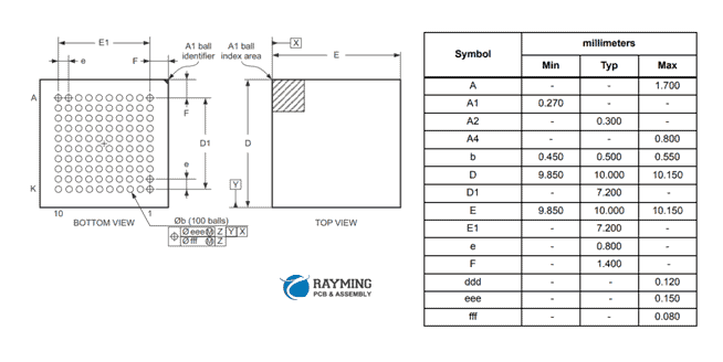
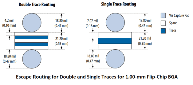
Ball grid array (BGA) packages have become a mainstay of modern electronics, offering high density interconnection in a small footprint. But properly laying out a printed circuit board for a BGA device does require special considerations versus other package styles. This article will provide guidance on key factors when designing BGAs including pad dimensions, placement, routing, thermal design, and board-level reliability. Following these PCB design recommendations will help ensure successful implementation of BGA packages.
Overview of BGA Packages
First, a quick overview of BGA technology:
Package surface mounts to PCB via an array of solder balls
Ball pitch ranges from 0.5mm to over 1.5mm
High density interconnection – Over 1,000 pads/balls
Thoroughly vetting the design avoids integration or production issues down the line.
Conclusion
Designing a PCB for a ball grid array device involves special considerations for routing, thermal management, manufacturability, and reliability. Following IPC guidelines and package-specific recommendations helps ensure your BGA implementation meets performance and quality standards. While requiring more planning, close collaboration between designer and manufacturer enables successfully deploying BGAs and gaining the benefits of the high-density interconnect technology in your products.
Frequently Asked Questions
Q: How fine of a pitch is achievable with newer BGA packages?
A: Packaging advances are enabling finer BGA pitches below 1mm, including 0.8mm and 0.65mm. This provides interconnect densities over 2500 pads/balls. However, PCB fabrication and assembly requires tighter tolerances at finer pitches which can increase cost.
Q: What are common solder ball materials used with BGA packages?
A: Solder ball alloys are typically eutectic SnAgCu (SAC). High lead solder is still used for some applications requiring high reliability. Lead-free solders are becoming standard due to regulatory pressures to eliminate lead.
Q: What are indications of potential BGA solder joint defects?
A: Excessive voids in solder joints, pad cratering, non-uniform or missing solder fillets, solder bridging, thermal pad dry joints, and cracked joints are defects that can lead to failures. X-ray inspection after assembly is recommended to identify issues.
Q: How many PCB layers are typically required for complex BGA designs?
A: High density BGA designs often require at least 6 to 8 layers. Critical signals need routing on inner layers with reference planes above and below. More layers provides additional routing channels to relieve congestion under devices.
Q: What are common causes of solder joint failures in BGA packages?
A: Thermal expansion mismatch, mechanical stresses, vibration, solder voids, dry joints, poor pad design, and moisture absorption can all contribute to eventual BGA solder joint failure over temperature cycling in the field. Following reliability design rules helps mitigate risks.
Printed circuit board (PCB) design is a complex process involving schematic capture, board layout, auto-routing, design rule checks, signal and power integrity analysis, thermal analysis, and much more. With products becoming more advanced, PCB designers need electronic design automation (EDA) tools that can handle rising complexity while improving productivity. This article will review ten leading PCB design software platforms available today based on features, capabilities, and ease-of-use.
Overview of PCB Design Flow
Before diving into the tools, let’s briefly summarize the typical PCB design flow supported by EDA tools:
Schematic capture – Draw the electronic schematic showing components and their electrical connections.
Symbol creation – Make symbols to represent components on the schematic.
Altium Designer is widely considered the most advanced and complete PCB design system available. It’s loaded with features spanning the entire design process from schematic capture to manufacturing outputs.
With unique innovations like ActiveRoute automated routing, Altium provides sophisticated capabilities that enhance designer productivity and workflow.
2. Cadence Allegro
Cadence Allegro offers a complete scalable PCB design environment targeted at high performance electronic applications. It contains advanced capabilities tailored for high speed design.
Key Features:
Robust design planning and process management
Constraint-driven design flow
Proprietary physical routing engine
Timing-driven layout tools
Extensive visualization capabilities
Flexible schematic editing tools
Interoperability with multiple analysis tools
library creation and management
Manufacturing output automation
Allegro provides high speed design capabilities critical for technologies like PCIe, Serdes, and DDR.
3. Mentor Graphics Xpedition
Mentor Graphics Xpedition enables enterprise-level PCB design addressing advanced users to casual occasional users. It is customizable and integrates with DFM tools for manufacturability.
Key Features:
High speed design features
Unified design environment
Manufacturing preparation automation
Custom reporting capabilities
Integrated library management
Scripting and automation
Multi-user collaboration
Interfaces to MCAD tools
DFx design guidance
Integrated PLM support
Xpedition balances high performance design capabilities with accessibility for a range of users.
4. OrCAD PCB Designer
orcad PCB
OrCAD PCB Designer provides a full PCB design workflow with specialized options for high speed, high density, and flex/rigid-flex boards. It offers advanced productivity features.
Key Features:
Constraint-driven, synchronized design flow
Interactive routing engine
Customizable DFM analysis
Real-time design feedback
Extensive component library ecosystem
High speed, signal, and power integrity analysis
Team collaboration capabilities
Custom reporting and scripting
Manufacturing output automation
OrCAD balances features and usability for cost-effective, capable PCB design. It integrates well across the entire electronics workflow.
Zuken CR-8000 is a proven PCB design solution for surface mount and complex multilayer boards. It features multi-board assembly and 3D packaging capabilities.
Key Features:
High speed design capabilities
Constraint manager for controlled flows
Multi-board assembly design
Photorealistic 3D visualization
Flexible layout editing tools
DFM analysis and verification
Library creation and custom reporting
Manufacturing documentation automation
Interfaces with MCAD tools
CR-8000 balances functionality with ease of adoption for seamless PCB design. The 3D packaging design environment helps streamline the electronics workflow.
6. Pulsonix PCB Design
Pulsonix PCB Design is an intuitive, easy to adopt platform with excellent usability. It offers advanced functionality like design reuse, manufacturing automation, and interactive routing suitable for many applications.
Pulsonix offers superb usability without sacrificing capable performance for mainstream PCB applications.
7. Autodesk EAGLE
Autodesk EAGLE is known for affordability combined with powerful features. Different pricing tiers allow customization for hobbyists, startups, and advanced users.
Key Features:
Easy to learn user interface
Extensive component libraries
Real-time DRC during routing
XML data exchange capabilities
Custom scripting and user language programs (ULPs)
Mixed-signal schematic and layout
Multi-sheet schematics
Integrated version control
Third party integrations via APIs
EAGLE continues gaining mainstream share given its balance of ease-of-use and capability at reasonable cost.
Pads Professional enables concept through production PCB design with powerful automation and reuse capabilities.
Key Features:
Rules and constraint-driven flow
Interactive routing engine
Sketch routing capabilities
Intelligent component placement
Integrated MCAD collaboration
Automated manufacturing documentation
Role-based design collaboration
Programmable automation interface
Packaged part reuse and automation
Library lifecycle management
PADS leverages automation and customization for efficient PCB design tailored to specific user needs and applications.
9. Solidworks PCB
Solidworks PCB provides a single integrated environment to support the entire electronic development process including MCAD collaboration.
Key Features:
Multi-board assembly design
Constraint-driven, synchronized workflow
Real-time DRC during layout
Integrated ECAD/MCAD component reuse
Automated manufacturing documentation
Design reuse and automation
Revision control and design history
Custom library development
Programmatic automation interface
Team collaboration capabilities
Solidworks PCB tightly couples the electronic and mechanical design workflows for streamlined product development.
10. Altium Concord Pro
Altium Concord Pro provides cloud-based PCB design capabilities accessible from any browser. It’s ideal for global team collaboration.
Key Features:
Cloud-based design environment
Managed component libraries
Interactive routing engine
Real-time design rule checking
Unlimited file storage and history
Automated outputs and documentation
Seamless team collaboration
Task management and notifications
Custom reporting and visualizations
Role-based access control
Dashboards and analytics
For organizations seeking a cloud-based PCB design platform, Altium Concord Pro is purpose-built for the task.
Conclusion
This lineup of leading PCB EDA tools demonstrates the breadth of options available today. From advanced capabilities like high speed signal analysis to cloud-based global team design, these platforms enable productivity and innovation across the PCB workflow. For organizations evaluating PCB design systems, this overview provides a starting point to narrow down your shortlist based on feature needs, budget, and electronic design culture and ecosystem. By matching organizational requirements to tool strengths and deployment models, engineering teams can leverage PCB design automation to achieve product goals and accelerate market success.
Frequently Asked Questions
Q: What are the main advantages of an integrated PCB design tool?
A: Integrated tools with unified schematic, layout, library management, and manufacturing capabilities reduce tool switching and streamline workflow. Integrated tools also enable greater synchronization between domains and automation across the design flow.
Q: How important are library and component management capabilities in a PCB design system?
A: Library capabilities are very important. Ready access to comprehensive component libraries speeds design time by eliminating repetitive symbol and footprint creation work. Library lifecycle management also assures designers access the right validated library elements rather than outdated or unapproved footprints.
Q: What training is required to become proficient in a PCB design tool?
A: Most tools can be learned in 40-80 hours of hands-on training. Learning the basic features can happen faster. But mastering advanced productivity tools and workflows takes longer. Formal training is recommended to gain proficiency faster. Some tool providers offer certification programs to document tool expertise.
Q: What are DRCs and why are they important in PCB design?
A: Design rule checks validate a PCB layout adheres to specified clearances, spacing, trace widths, and other constraints. DRCs are critical for ensuring manufacturability, reliability, and performance. DRCs integrated into the tool avoid surprises late in the design process.
Q: How does Revision Control help with PCB design?
A: Revision control systems record incremental changes and provide version history. This supports parallel workflows and tracks design progress. Revisions enable designers to experiment without risk of losing working baselines. Integrated revision control improves design team collaboration.
Gerber files are the industry standard format for printed circuit board (PCB) manufacturing. They provide all the information a PCB manufacturer needs to fabricate your board, including copper layers, solder mask, silkscreen, drill data, and more. As a PCB designer, you’ll need to be able to generate Gerber files from your EDA (electronic design automation) software to send your finished board layout off for production. This comprehensive guide will walk you through the entire process of exporting Gerber files, from understanding the different file types to setting up your layers correctly. With the right preparation, you’ll be able to produce the accurate Gerber files required to turn your design into a physical reality.
The Gerber Format
Gerber files use a standardized numeric format (RS-274X) to convey PCB layout data like images, coordinates, and commands. The files describe each layer of the board layout separately, such as copper, silkscreen, solder mask, drill holes, etc. By separating the data into different files, PCB manufacturers can selectively choose which layers to image during the fabrication process. This eliminates the need to rebuild the entire board layout from a single massive data file.
Vector Images – Gerber files use vectors to describe shapes like lines, arcs, and circles that make up tracks and outlines. This makes the format very compact compared to bitmapped images.
Apertures – Apertures define the size and shape of the vector. They allow features like pad diameters and track widths to be adjusted by simply changing the aperture.
Coordinates – Each vector endpoint is defined by X and Y coordinates that locate features accurately. The coordinates use metric units down to nanometer precision.
RS-274X Language – Standardized commands are used for selecting apertures, setting coordinates, interpolating lines/arcs, etc.
By adhering to the standardized RS-274X format, Gerber files can be loaded directly into PCB fabrication equipment without the need for conversion or preprocessing. This avoids errors and keeps the data intact as it moves through the manufacturing process.
A fabricated PCB is made up of a number of physical layers that are stacked and bonded together. Gerber files are required to define the data for each individual layer. Here are some of the most common layer types:
Copper Layers
The copper layers contain the conductive tracks, pads, and vias that make up the circuit. There is often a top and bottom copper layer, and also inner layers if using a multilayer board. Each copper layer has its own Gerber file.
Solder Mask Layers
Solder mask is the protective coating that is applied over the copper to prevent solder bridges. The solder mask layers are essentially negative images that define the areas where solder mask should be absent (such as over pads).
Silkscreen Layers
The silkscreen is decorative printing on the PCB. It is used for markings like component designators, logos, board outlines, etc. Silkscreen layers use the Gerber format to define the graphics to be printed.
Drill Files
Drill files specify the locations and sizes of holes to be drilled in the PCB. This includes through-holes for component leads as well as non-plated mechanical holes. Excellon is the most common drill file format.
Assembly Drawings
Assembly files define pick and place data for population of components on the bare PCB. This aids automated assembly and is optional for basic fabrication.
Project Setup Guidelines
Before you can generate proper Gerber files, the PCB project needs to be set up correctly. Here are some key guidelines to follow:
Coordinate System
The coordinate system used should match the PCB manufacturer’s specifications:
Origin – Bottom left corner of the board
Axes – X horizontal, Y vertical
Units – Metric (mm)
Rotation – No rotation
This avoids extra processing by the fabricator to align to their system.
Layer Stackup
The layer order and materials should follow the fabricator’s layer stackup convention. A typical example is:
Top Silkscreen
Top Solder Mask
Top Copper
Inner Copper Layers…
Bottom Copper
Bottom Solder Mask
Bottom Silkscreen
Consult your manufacturer’s guidelines and match the sequence in your EDA tool.
Design Rules
Set your track widths, clearances, via sizes, etc. to comply with the fabricator’s design rules for the selected PCB technology. This ensures the layout is manufacturable.
Net Names
Use a consistent naming convention like “GND”, “VCC”, “+5V” for power nets. Avoid changing net names mid-trace as this can confuse fabrication data.
Output Generation
Gerber Files
Once the project is properly configured, generating the Gerber files is straightforward. Here is the general process:
Cam File Generation
Your EDA tool will have an option to generate cam, photoplot, or fabrication output files from your board layout. Select the appropriate output profile that matches your board technology (e.g. “2 Layer FR-4”). This will generate all required layer Gerber files along with drill, netlist and other fabrication data.
Layer Checking
Thoroughly inspect each layer file to ensure the contents match the source PCB layout. Check for missing traces, incorrect apertures, misaligned layers, etc. Any errors can lead to costly fabrication mistakes.
File Naming
Give the output files clean, consistent names indicating the layer type and order sequence:
TopSilkscreen.gbr
TopSolderMask.gbr
TopCopper.gbr
…
Avoid using spaces, special characters, and overly long names.
Compressing and Archiving
Zip/archive the complete set of Gerber files together for easier transfer. Avoid compressing individual files as it can confuse CAM systems.
Transferring to Manufacturer
Upload the Gerber archive to the PCB manufacturer through their website portal or send via email. Wait for the files to be checked before proceeding with your order.
Follow these tips to avoid common mistakes and ensure your Gerber files generate accurately:
Stay Organized – Keep your PCB layers well structured and named consistently through the design process. Disorganization leads to data mix ups.
Follow Standards – Use the manufacturer’s recommended stackup, design rules, and layer settings. Never deviate unless approved.
Design Rule Check – Run DRC on your board layout and fix any errors before generating output files. This catches problems early.
Double Check Layers – Verify critically that each layer matches your source data. Don’t rely on the CAM process blindly.
Communicate Changes – Inform your manufacturer if you need to revise the Gerber files after initial submission. Send the full updated set.
Learn from Experience – If you have fabrication issues with your first builds, analyze the cause and improve your Gerber generation process.
Gerber File Viewing and Verification
Since Gerber files contain crucial fabrication data, it is essential to review them carefully for potential problems before sending them out. Here are some tips on how to validate your Gerber files:
Use a Gerber Viewer
A Gerber viewer is specialized software that loads the standard RS-274X files and renders the visual contents for inspection. This provides the most realistic validation of how the manufactured PCB will turn out. Some good free options are GC-Prevue and Gerbv.
Check Layer Alignment
When overlaying layers in a viewer, check that features line up properly across layers. Misalignments lead to etched copper being in the wrong place.
Inspect Apertures and Graphics
Verify apertures are sized correctly and vector graphics render sharply without glitches. Any artifacts could indicate aperture, format, or resolution issues.
Compare vs Source File
Overlay the Gerber layers atop your source PCB data to compare signal-to-signal. Any discrepancies in tracks or pads will show up.
Analyze DRC Reports
Even if your source file passes DRC checks, run DRC on the Gerber files themselves. The CAM process can sometimes introduce new errors.
View Drills & Holes
Inspect drill layers to ensure hole sizes are correct and holes align precisely with pad stackups.
Confirm Critical Data
Double check critical identifiers like designators, component outlines, board dimensions, and text are rendered clearly and without errors.
Thorough Gerber file inspection is the last line of defense against expensive PCB fabrication errors. Spending extra time validating can save you money and headaches down the road.
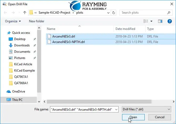
While Gerber files define the layered 2D data of a PCB layout, drill files specify the actual hole sizes and locations required to fabricate the board. Excellon (.drl) is the standard format for drill data. Here is an overview of how drill files are derived from Gerber:
1. Identify Hole Locations
The locations of all required holes are determined from the component pads and vias defined in the Gerber copper layers. PCB CAM tools extract the X/Y coordinates of every pad/via.
2. Define Hole Sizes
Each pad or via has a associated finished hole size defined during PCB layout. These hole sizes are mapped to the extracted hole locations.
3. Optimize Hole Grouping
To optimize the drilling process, holes are grouped into “tool lists” based on having the same drill bit size. This minimizes tool changes.
4. Generate Excellon File
The formatted Excellon file (.drl) is output containing tool definitions and hole coordinates. The data is organized to facilitate efficient drilling.
5. Add Routing Attributes
Additional routing attributes direct the PCB drilling machine like spindle speeds, tool change positions, and drill cut depths for partially drilled boards.
6. Validate vs Gerber Layers
It is critical to validate the drill file against the source Gerber data to ensure the proper hole sizes and locations transfer over as expected.
With an accurate drill file derived from the layout, the PCB manufacturer can drill all holes to precisely match up with the layered circuit board data.
For complex PCB projects, additional steps and advanced Gerber techniques may be required:
SolderPaste Files
Solder paste files indicate the precise solder paste distribution required to place and solder surface-mount components. This is often defined as a separate layer.
Removing Explicit Zeroes
Certain CAM systems can misinterpret surplus “zero” command codes. Stripping these out avoids problems.
Simplifying Apertures
Reducing the number of unique apertures in the files helps performance for some fabricators. CAM tools can consolidate apertures.
Polarity Markings
For double-sided boards, adding a small “polarity mark” hole at a standard location aids in orienting and aligning layers.
Routed Tab and Panel Design
Panelization features like tooling tabs, mouse bites, and break-off rails are added for PCB depanelization.
Layer Alignment Markings
Fiducials that appear on multiple layers can provide visual cue points for aligning layers during fabrication.
As you gain experience, continue exploring new Gerber techniques to enhance your fabrication capabilities. The standard allows ample flexibility.
Conclusion
Gerber files are integral to turning your completed PCB layout into a physical board. By understanding the specialized data format, planning your project correctly, thoroughly inspecting your files, and employing advanced techniques, you can generate accurate Gerber files the first time. With clean, error-free data, you will avoid costly delays and re-spins during fabrication. Spending extra time up front to polish your Gerber file creation process ultimately saves you frustration, time, and money further down the line.
Summary of Main Points:
Gerber format uses succinct vector data to convey PCB layout information layer-by-layer.
Typical layers include copper, solder mask, silkscreen, drill data. Each must have a Gerber file generated.
Set up your PCB project according to manufacturer’s guidelines for flawless data output.
Carefully inspect all layers for alignment errors or missing data before sending files out.
Excellon drill files are derived from copper pad/via locations and holes sizes defined in your layout.
Advanced techniques like solder paste layers and panelization require additional data.
Take time to refine your Gerber generation process and you’ll produce fabrication-ready files the first time.
Frequently Asked Questions
Why are Gerber files needed for PCB manufacturing?
Gerber files are the standard format that PCB fabrication equipment understands. The files provide the precise layered data needed to image the conductors, solder mask, markings, drill locations, etc. without errors. Trying to fabricate directly from CAD or source layout files would be prone to mistakes.
How accurate are the coordinates in Gerber files?
The Gerber format supports metric coordinates to a precision down to ten nanometers. This allows traces, pads, and holes to be located extremely accurately for high density PCB designs. The precision avoids rounding errors over long distances.
Can you edit Gerber files?
While it is possible to make edits to Gerber files with specialized tools, it is not recommended. The ideal workflow is modifying the source PCB layout, then regenerating clean Gerber output. Direct Gerber edits often lead to conflicts between layers.
What are the main advantages of Gerber X2 format?
Gerber X2 allows greater precision, smaller apertures, step and repeat panelization, embedded component and net properties, and other enhancements. However, adoption of X2 has been slow since traditional RS-274X works well.
How are irregularly shaped traces defined in Gerber files?
Irregular pad/trace geometries are approximated using very short vector segments. Smaller segment lengths increase the precision but also increase file size. There is a tradeoff between accuracy and efficiency.
1.Gerber Files Introduction
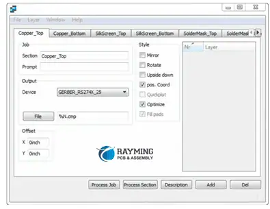
Gerber file format is a defacto standard used by PCB manufacturing industry. This is analogous to produce a *.pdf file after designing a graphics or text document. Almost everyone who is involved in PCB design either hobbyist or commercial designer may have used it. It is actually an ASCII file format.
Gerber file format is evolved from applications where it is used to re-create images or graphics i.e., printers and plotters industry. In the same way it is used in electronics hardware industry to print PCB tracks, holes, clearances and all information which is contained in a *.pcb design file. The leading PCB CAD softwares are able to create gerber files as an output of PCB design file. These softwares generally use RS-274-X Gerber file format because it is newer and easy to handle data files.
The softwares have a feature to execute gerber output generate command. Usually, it is a dialogue box which has enable and disable options to include and exclude certain layers and parameters to include or exclude from gerber output files. In RS-274-X file format one file is produced for each one layer of PCB design file.
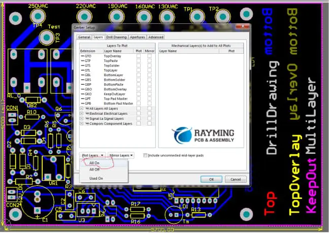
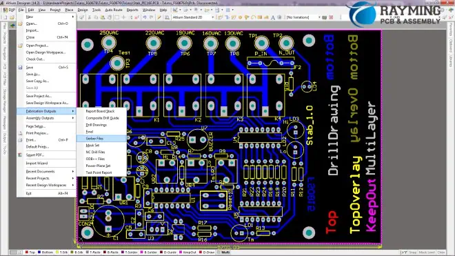
The gerber files generator can be launched from (PCB editor) Tools> Generate Gerber files command.
The following CAM Options dialogue box opens:
Figure 1: Setup for Gerber output
However, every software has its own style of creating Gerbers files. They may have small differences compared to others to execute commands. Set of commands that how to generate Gerbers in specific software are best explained in the respective software manual. This example is produced to guide about the process step by step.
The dialog box in Figure 1, produces settings for location to save output gerber files. Almost all PCB designers know to set the folder and file path in a desktop computer.
Figure 2: Gerbers Settings Dialogue Box
The dialogue box in Figure 2, appears to make settings that what to include in the gerber files command, if executed. The first pane makes resolution of scan. The description below to the dialogue box is self-explanatory and can be chosen by clicking the respective radio-box. Higher resolution occupies more memory but have better data precision. There are two settings: the metric (mm) system and imperial (inches) system of units. Gerbers in both formats can be generated. However, for data clarity and to be safe side, generate Gerbers in both mm and inches format, in two separate folders with clearly mentioning their units type.
The next pane in this dialogue box is layers settings where different layers can be enabled to include or exclude in the output files. Generally, it is a good option to “enable all used layers”.
Drill drawing and mechanical layers panes make settings about drill drawing and mechanical layers respectively.
Apertures settings is used for thickness of tracks used and advanced is used some other settings. For producing gerber files it is a good practice to consult with your PCB manufacturer.
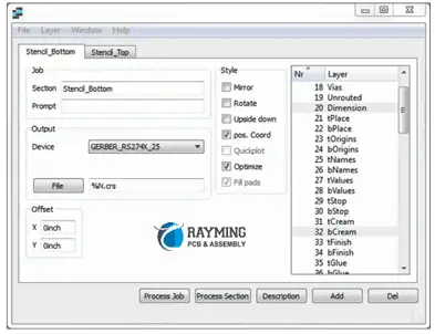
Figure 3: Settings Dialogue Box for NC drill files
The NC drill files setup produces PCB holes location and drill size information just like the gerber files i.e., location and size of drill. This also has the same settings and parameters as in Gerber files step. Produce the NC Drill files alongwith gerber files.
In a gerber file following layers and information should be added:
Signal layers: All signal layers which are used in the PCB design or those carry electrical signals should be enabled to produce its gerber file.
Plane layers: Similar to signal layers all plane layers should also be enabled to produce gerber output files. These are solid coper layers which distribute power.
Keepout layer: Keepout layer is electrical boundaries of the board. This can also be used to board cutting boundary.
Mechanical layers: The used mechanical layers should also be enabled. A mechanical layer may not have any electrical information like in signal layer or plane layers. However, they can have some information about mechanical parameter like PCB cutting or fixing in enclosures.
Overlays: The top overlay and bottom overlay which have information of components designators and other PCB nomenclature notes.
Dimensional Information: PCB Dimensions information should be added on top overlay or mechanical or keepout layer of PCB design file before generating gerber files.
Layer stackup: Before generating gerber files add layer stackup information in any enabled mechanical layers so that manufacturer can use information about PCB material such as base material thickness, pre-preg thickness type etc.
Preferably produce time and date stamped Gerber files so that they would be back traced for any query.
Recheck and verify the file types using any gerber viewer software tool.
If found accurate and forward to the manufacturer.
Figure 4: Gerber files enable and disable and extensions
Figure 4 shows the enable and disable of different layers view in gerber file setup dialogue box .
4.Summary:
The gerber file format is a defacto standard of interface between a PCB Design engineer and manufacturer. Gerber format is RS-274-X 2D ASCII file format. It includes all conductive, mechanical, text and keepout layers information of a PCB design alongwith necessary notes for manufacturing.
The RS-274-X format produces one file for each layer of PCB and is preferred by the PCB industry. It is designer’s responsibility to add layers carefully to generate files. Any confusions and wrong data may cause an surprised and unwanted PCB that may be garbage only.
EAGLE (Easily Applicable Graphical Layout Editor) is a popular PCB design software used by engineers, hobbyists and students. It provides a seamless workflow from schematic capture to PCB layout and includes powerful features for generating manufacturing files. This article provides a comprehensive guide on exporting Gerber files from an EAGLE PCB project.
Overview of Gerber Files
Gerber files are the industry standard for transferring PCB design data to fabrication and assembly units. Here are some key facts about Gerber files:
Contain vector image data of PCB layers like copper, mask, silkscreen, drill files etc.
Use RS-274X file format with .gbr extension.
Provide image plots of fabrication layers for photoploting.
Required by PCB manufacturer along with drill files to manufacture the board.
EAGLE uses extended Gerber format RS-274X with additional features.
CAM Processor Settings
Before generating Gerber files, the CAM processor settings must be configured in EAGLE to specify file outputs. This is done through the CAM editor.
The important CAM job settings are:
File Format – Extended Gerber RS-274X.
Coordinates – Absolute or Incremental depending on manufacturer requirements.
Leading and trailing zeros – For consistent file formatting.
-asymperc Output directory – Location to save output files.
File naming convention – Unique names for identification.
Layer mapping – Links board layers to Gerber files.
Additional outputs – Like drill files, drawings etc.
Properly setting up the CAM job is essential for clean and error-free Gerber generation.
Maintaining proper version control of Gerber files is essential:
Increment version number in CAM job file naming convention.
Include version number in file name or as comment within file.
Track versions in documentation.
Save prior versions in archive directory.
Proper versioning avoids mix up or use of outdated files.
Conclusion
The CAM processor in EAGLE provides a streamlined workflow to generate industry-standard Gerber files from a PCB design. Configuring appropriate settings and layer mapping produces a fabrication-ready set of Gerber images and drill data. Proper validation ensures accuracy while features like panelization and version control enhance manufacturability. A sound understanding of the Gerber file generation process enables PCB designers to hand-off error-free files to fabrication, leading to smooth prototype builds or production.
FAQs
What are some common issues observed in Gerber files?
Missing copper or silkscreen details, incorrect apertures, wrong polarity and layers mapped to incorrect files are frequent Gerber issues.
How can panelization help reduce PCB assembly cost?
Panelizing allows multiple boards to be populated and assembled together. This lowers setup overheads and improves throughput, reducing overall cost.
What information should be included in Assembly drawings?
Assembly drawings include component outlines, designators, polarity markings, fabrication notes and other build instructions.
Why is validation of drill files important?
Drill files must match hole sizes and locations designed in PCB to avoid incorrect drilling. This can lead to lack of hole alignment during assembly.
How can Gerber files be compressed?
EAGLE CAM allows zipping output files. Gerber data can also be compressed after generation using utilities like gzip.
1.PCB Manufacturing Pre-requisites
The Gerber RS-274X file format is used for PCB manufacturing data submission to fabrication house. This is output of PCB design file. Why not PCB Design file handed over to manufacturer? One of the reasons is almost all product hardware concept related information is present in PCB design file. For example, Bill of Material can be very easily generated from this PCB design file. It contains active connectivity information from where entiredesign can be copied. The gerber files do not include BOM and active connectivity information. The gerber files are image of active layers and connections but they are just “images of all active PCB layers”.
So they are relatively safe to submit to third parties such as PCBs fabrication houses etc.The gerber format was emerged from applications where it was applied to re-generategraphics or images i.e., from plotters industry. It isused in electronics PCBs manufacturing industry in the same way. It generates PCB traces, pads, vias, clearances and all other electrical and non-electrical information contained in a design file. All PCB CAD softwares are capable to generate gerber files.All the electronics engineers who have designedand manufactured PCBs will have used this option.
The PCB manufacturer creates photo plots from the given Gerber files data. The higher the resolution of gerber files data the better the plots created for PCB fabrication.
2.What should include in Gerbers
The gerber data is very critical to produce. It should be generated very carefully. Usually, any layer missed during gerber files generation will interpreted by manufacturer that there was no layer in the original design. The PCB produced will be off course faulty and cannot be used. A faulty gerber data will produce faulty PCB output.Before generating gerber files in Eagle software the PCB design engineer should very clear to include necessary layers ad information in Gerber CAM processor of Eagle software.
3.Eagle Output File Format
The eagle PCB Design software generates gerber files on popular RS-274X format however it is slightly tricky to understand the file extensions. The drill files are created and saved separately in Exelon format. For gerber files creation it provides a separate software utility called CAM (Computer Aided Manufacturing) processor or only processor.
In eagle there are two main terms the processor and the job. The processor is explained already. The job is a set of tasks composed so that each task reads specific layer information from PCB design file and creates gerber file.
CAD softwares create one file for each PCB design layer. So for 20-conductive layers PCB design there will be 20 gerber files, additive to top and bottom legend, keepout, top and bottom paste, top and bottom solder mask layers. When it is to submit data for manufacturing or quotation purposes the Gerber files folder should be in*.zip or *.rar format.In Eagle software the following extension for layers are produced in gerber generation.
6 layer board also need internal layers information also
GL2 Inner Layer2
GL3 Inner Layer3
GL4 Inner Layer4
GL5 Inner Layer5
Along with layers information, holes location and size of drills also part of gerber data produced before submission to a manufacturer. It is called NC drill file and data is incomplete without these files. The purpose of Gerber files is to create X/Y Coordinates, Configuration Parameters, Drawing Commands and Aperture Definitions of each layer mentioned in software. The Eagle software scans the each layer entire PCB file to create these four parameters for each separate layer.
4.CAM Processor
However, to generate a PCB Design file into CAM Processor:
Usually, the CAM processor is a dialog box that takes design file as an input and allows optional settings and generates output files.
To open CAM Processor click File> CAM Processor
OR alternatively, in Control Panel’s main menu File > New > CAM Job
thenselect PCB board: go to file> selecta job file>execute the job.
For fabrication data to be handed over to manufacturer it is necessary that it should be accurate and complete. Ay missing information will cause a faulty and hence garbage PCB.Eagle software like other softwares produces files in Gerber RS-274X format. For successful gerber files creation one should have clear knowledge of Eagle CAM processor. It is a good practice to verify metadata files against each layer with their three charactersextension.For gerber data verification known online and offline installable softwares are available which show the exact image what data is generated. Verify and match gerber data before submitting it to fabrication house. Besides PCB layers metadata NC drill files are also required by the PCB fabrication house so produce separately, verify and match with original design file before forwarding it.3
RS-274-X Gerber file format is a defacto data sharing standard for PCB manufacturing. This is basically a printer or plotter language which is used for PCB CAM (Computer Aided Manufacturing) data generation. Almost everyone who uses Altium Designer software for PCB design, either hobbyist or commercial designer, may have used this feature. It is actually a 2D ASCII file format.
Gerber file format is evolved from applications where it is used to re-create images or graphics i.e., printers and plotters industry. In the same way it is used in electronics hardware industry to print PCB tracks, vias, pads, text, holes, clearances and all information which is contained in a *.PcbDoc design file. The Altium Designer software tool has a feature to create and gerbtool option to verify data as well.
Like other softwares outputs the Altium Designer gerber file can be divided into four subparts:
Configuration Parameters
Aperture Definitions
Drawing Commands
X/Y Coordinates
Each file extension denotes a specific layer such as:
In Gerber setup dialogue box Set file producing unit system.
In layers pane add layers to be re-produced in gerber format.
In drill drawing pane click plot all used layer pairs on both of the boxes.
Set apertures box.
Set advanced parameters in advanced pane or otherwise keep default settings.
Click ok , it generates the gerber outputs in the project folder.
On same method NC drill files are created i.e., File>Fabrication Outputs> NC Drill Files and then adopt the same steps as above.
Or in other way it can be generated by following steps:
Output Job File to project > Fabrication Outputs> Gerber Files and then set path for files.
Double click “Gerber Files” it will open Gerber setup. Use the same steps as above and click ok.
Enable output generate option and set target folder location.
Clock Run or double click over generates content. The gerber file outputs will be generated.
Figure 1: Sample PCB Design file
In figure 1 different layers names are shown in their respective layer. The same layers can be viewed in the final view Figure 5 as Gerber output generated.
In a gerber file following layers and information should be added:
1- Enable all signal layers which have been used for routing in PCB design or those which have electrical signals routing should be enabled to re-produce in gerber format.
2- Enable all plane layers which are solid copper and distribute power to the circuit on PCB. These are printed as negative image of layer.
3- Enable Keepout layer, it is usually electrical boundary of the board. The keepout can also be asked to manufacturer for cutting boundary.
4- Enable required mechanical layers in gerber setup. A mechanical layer does not have any electrical information like in signal layer or plane layers. However, they can have some information about mechanical parameter like PCB cutting or, 3D PCB footprints information, assembly and fixing in enclosures etc.
5- Enable Top Overlay and Bottom Overlays which have information of components designators and PCB name, number, nomenclature debug information and test signal details etc.
6- Dimensional Information: PCB Dimensions information should be added on top overlay or mechanical or keepout layer of PCB design file before generating gerber files.
7- Layer PCB stackup: Before generating gerber files add layer stackup information in any enabled mechanical layers so that manufacturer can use information about PCB material such as base material thickness, pre-preg thickness type etc.
8- Preferably produce time and date stamped Gerber files so that they would be back traced for any query.
9- Recheck and verify the file types using any gerber viewer software tool.
10-If found accurate and forward to the manufacturer.
Figure 6: Gerber files enable and disable and extensions
Figure 6 shows the gerber files produced by Altium Designer software, produced time, type of layer etc.
Gerber format is RS-274-X 2D ASCII file format. The gerber file format is a defacto standard of interface between a PCB Design engineer and manufacturer. It includes all conductive, mechanical, text and keepout layers information of a PCB design alongwith necessary notes for manufacturing.
The Altium Designer software produces RS-274-X format Gerber files by different methods. The latest software and updates about files generation are available on Altium ®. In this tutorial a complete yet comprehensive guide has been provide.
Introduction
Gerber files are the standard format used to transfer PCB design data to fabrication and assembly units. Altium Designer has robust capabilities to generate industry-standard Gerber files needed for board manufacturing. This article provides a detailed guide on the process of exporting Gerber files from an Altium PCB project, with additional tips for file settings and customization.
Gerber File Basics
Gerber files represent PCB layout data in a vector graphics format that can be interpreted by fabrication machines. Here are some key facts about Gerber files:
Developed by Gerber Systems in the 1960s, hence the name.
Contain vector-based information to image PCB layers.
Used for photoplotting fabrication layers on film or directly on boards.
Required by PCB manufacturer along with drill files for board fabrication.
Output Job File Settings
Before exporting Gerber files, the key output job settings in Altium must be configured. This is done through the OutJob editor by going to File > Fabrication Outputs > OutJob Editor.
Various options like coordinates, zero suppression etc.
The most critical settings are layer stack and layer specifications which determine the actual layers output.
Generating Gerber Files
Once the OutJob is defined, we are ready to export the Gerber files. This involves simply running the output job to generate all the required layers.
The steps are:
Open the PCB project in Altium and go to File > Fabrication Outputs > Generate Gerbers.
Select the OutJob in the Gerber Job Editor window.
Click on Validate outputs – this checks for any errors or missing data.
If validation passes, click on Generate to run the job and output Gerber files.
The Gerber files can be found in the specified output folder location.
By default, a .PDF and .ZIP archive of the files is also generated.
For quick one-click Gerber generation, the OutJob can be added to the Project menu for the PCB. This automates opening the job editor and executing the output process.
Layer Stack Settings
The layer stack regions defined in the OutJob determine which layers are combined to generate the final Gerber files.
Using these layer stacks, all required Gerber files can be generated. Additional stack-ups can also be defined.
Layer Specifications
Layer specifications determine which layers actually get included in a layer stack while generating outputs.
Typical layer inclusions for standard PCB file outputs:
Layer Stack
Layers Included
Top Layer
Top Layer + Multi-Layer
Bottom Layer
Bottom Layer + Multi-Layer
Internal Layers
Inner Layers + Multi-Layer
Top Solder
Top Solder + Coverlay Top
Bottom Solder
Bottom Solder + Coverlay Bottom
Top Overlay
Top Overlay + Coverlay Top
Bottom Overlay
Bottom Overlay + Coverlay Bottom
The multi-layer and coverlay combinations merge the signals and plane layers appropriately. Additional specifications like keep-outs can also be added.
Layer identifier – TL for Top Layer, TS for Top Solder etc.
File Suffix – Can include version number, date etc.
For example: ProjectABC_TL_Rev1.gbr
This provides a unique ID for each layer file. Similar naming can be applied to drill files.
Important Plot Layers
Some of the key Gerber layers required for fabrication are:
Top and Bottom Copper Layers – Carry signals and traces
Internal Plane Layers – Power, ground and routing layers
Top and Bottom Solder Mask – Defines solderable areas
Top and Bottom Silkscreen – Component markings and legends
Board Outline – Dimensions of finished board
Drill Drawing – For NC drill machine
Drill Data – Size and location of drilled holes
Additional Outputs
Besides standard Gerber layers, additional outputs like the following can also be generated:
Copper thickness table – Specifies finished copper thickness for each layer
Netlist file – Connectivity information for test and analysis
Assembly drawings – Help guide component placement
PCB 3D model – For design visualization
Fabrication and Assembly drawings – Includes callouts, notes, etc.
Impedance information – For controlled impedance designs
Stackup details – Layer materials, properties and sequence
File Validation
Before sending to PCB fabrication, the Gerber files must be thoroughly validated using the following checks:
Visual examination – Open files in Gerber viewer to check if layers contain the expected images.
Preflight tests – Use preflight tools to verify file format, aperture settings etc.
CAM tool checks – Use CAM software to check file opening, merging and editing.
Test photoplots – Get film photoplots made from files to validate image accuracy.
Compare netlist – Use netlist file to check all connections in design are properly imaged.
Design rule check – Ensure critical clearances are maintained in generated images.
File Optimization
Gerber file optimization involves tweaking settings to get smaller files while retaining image quality. Main techniques include:
Selecting optimal resolution and image settings.
Using zero suppression to reduce file size.
Applying data compression while exporting files.
Removing duplicate drawing data and unused apertures.
Merging layers where possible to reduce file count.
Proper optimization ensures faster file transfers and processing while minimizing storage requirements.
Conclusion
Comprehensive Gerber file generation tools within Altium allow creating all fabrication data needed to manufacture a PCB easily and efficiently. Configuring suitable OutJobs, layer stacks and file settings produces industry-standard outputs that can be directly sent for board fabrication. Validation checks must be performed diligently before file release to avoid errors reaching manufacturing stage. Overall, mastery over the Gerber generation process is crucial to harness the full power of Altium and seamlessly progress from design to fabrication.
FAQs
What are some common problems observed in Gerber files?
Missing copper, malformed apertures, incorrect filenames and layers in wrong files are common Gerber issues. Preflight tools help catch such errors.
How to check if a specific layer is getting correctly output in Gerbers?
Open that Gerber file in viewer and check if key shapes or test structures added to the layer are present in output image.
Why zipping is recommended for Gerber file transfer?
Zipped files occupy less storage space. Zipping also reduces chances of file corruption during internet transfer using protocols like FTP.
What is the difference between PCB fabrication drawing and assembly drawing?
Fabrication drawing guides board manufacture while assembly drawing is used for component placement, annotations during PCB assembly.
How can gaps be avoided between copper layers and planes in Gerber data?
Enable the Remove islands option in Layer Stack Regions. Use proper Positive and Negative layers to define extents.