How Big is the FPGA Market?

FPGA Market

Introduction

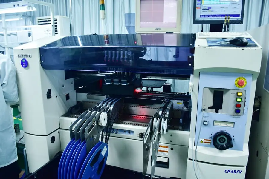
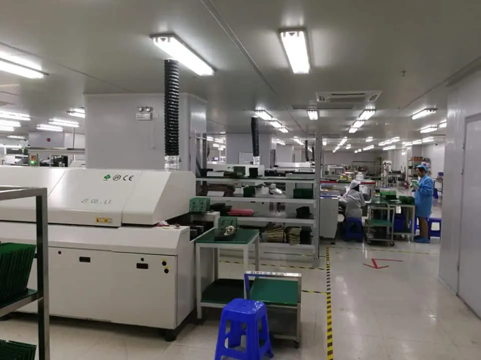
Field Programmable Gate Arrays (FPGAs) are semiconductor devices that can be programmed and reconfigured to desired application or functionality requirements after manufacturing. The flexibility of FPGAs makes them valuable for prototyping and testing circuit designs, as well as implementing hardware acceleration or custom logic in a wide range of industries. This article examines the current size and growth projections of the global FPGA market.

FPGA Market Size

YouTube video

The FPGA market was valued at $5.35 billion in 2019. According to most analyst projections, the market is forecast to grow at a CAGR of 9% – 12% between 2020 to 2025, reaching over $8 billion by 2025.

Here is a summary of recent FPGA market size estimates:

Firm2019 Market Value2025 Market ProjectionCAGR
Stratistics MRC$5.35 billion$8.62 billion~12%
Fortune Business Insights$5.4 billion$9.1 billion10.3%
Mordor Intelligence$5.33 billion$7.9 billion8.3%
Technavio$4.9 billion$8.2 billion10.7%

The consensus from major market research firms is the FPGA market in 2019 was between $5-5.5 billion, with projected growth to reach $8-9 billion by 2025. This represents a healthy compound annual growth rate of approximately 9-12% over the next 5 years.

Key drivers fueling this growth include:

  • Proliferation of IoT connected devices requiring edge intelligence
  • Adoption in data centers for hardware acceleration
  • Demand for ADAS and autonomous vehicle capabilities
  • Aerospace/defense electronics innovation
  • Rising complexity of chip designs requiring prototyping
  • Expansion of 5G infrastructure dependent on FPGAs

The FPGA market declined in 2020 due to global economic challenges, but rebounded sharply in 2021. Growth is expected to accelerate over the next decade with new tailwinds such as artificial intelligence, networking infrastructure, and advanced driver-assistance systems.

FPGA Market Share

The FPGA industry is highly concentrated, with Xilinx and Intel/Altera comprising 80-90% of total market share:

CompanyEstimated Market Share
Xilinx50-60%
Intel/Altera30-40%
Microchip (Formerly Microsemi)5-10%
Lattice Semiconductor1-2%
Others1-2%

Xilinx has held the dominant position in FPGAs for decades. Intel gained significant share after acquiring Altera in 2015, making them a strong second player. Microchip (Microsemi), Lattice Semiconductor, and a few other smaller companies make up the remainder of the market.

The high cost of developing FPGA fabrication processes presents a significant barrier to entry, making it difficult for new competitors to enter and gain share. The technology and IP involved in advanced FPGAs also makes them hard to displace once a supplier is designed into an OEMโ€™s systems. These dynamics contribute to Xilinx and Intelโ€™s continued duopoly control of the industry.

Market Segmentation by Type

FPGAs can be segmented into different categories based on their underlying architecture and capabilities:
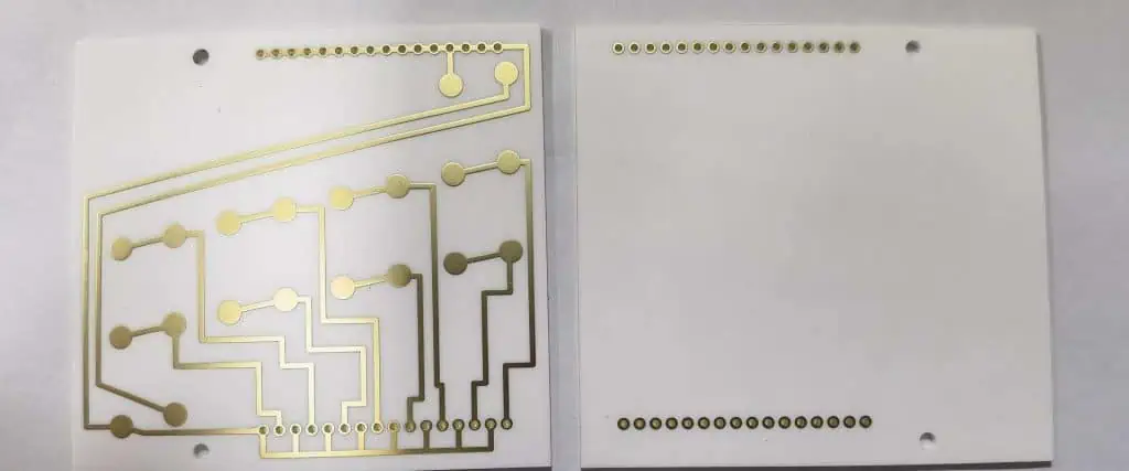
SRAM-Based FPGAs

SRAM-based FPGAs use static RAM configuration cells to program logic blocks and I/O pins. SRAM allows infinite reconfiguration but loses programmability when power is removed. Mainstream FPGAs from Xilinx and Intel are based on SRAM architecture.

Flash-Based FPGAs

Flash-based FPGAs use nonvolatile flash memory for configuration, retaining functionality without power. This approach has reliability advantages but does not enable modification as freely as SRAM FPGAs. Microsemi (now Microchip) is the main supplier of flash-based FPGAs.

Anti-Fuse FPGAs

Anti-fuse FPGAs use a one-time programmable method to create permanent connections between logic elements. This provides security and assurance that the FPGA cannot be reprogrammed later. Anti-fuse FPGAs are popular for military/aerospace applications.

SRAM-based FPGAs dominate the market currently with over 90% share. However, new flash and anti-fuse architectures are emerging for different application requirements, and gaining adoption in niches like automotive or IoT.

Market Segmentation by Application

FPGAs are utilized across a diverse range of vertical applications. The major end-use categories are:

Data Processing:

FPGAs are widely adopted in data center acceleration for tasks like encryption/decryption, compression, and AI inferencing. Intel and Xilinx both now offer FPGAs targeted for data center usage.

Aerospace and Defense:

The anti-tamper and radiation resistance abilities of FPGAs make them essential for space systems, missiles, satellite communication, and other defense projects. Xilinx and Microsemi(Microchip) have a strong customer base in aerospace/defense.

Wired and Wireless Communication:

FPGAs are crucial for prototyping and implementing the sophisticated signal processing required in modern communications systems. This includes 4G/5G infrastructure, as well as broadband cable and fiber networks. Major customers include Huawei, Ericsson, Nokia, and Cisco.

Industrial Automation:

For industrial control, robotics, and Industry 4.0 systems, FPGAs enable the advanced parallel processing required for precise monitoring and actuation. Lattice Semiconductor targets the value FPGA segment for industrial automation.

Automotive:

FPGAs are increasingly used in driver assistance, infotainment, connectivity, and powertrain systems as cars become more electronic. Xilinx and Intel have growing automotive FPGA sales.

Consumer Electronics:

FPGAs have adoption in consumer applications like smartphones, tablets, cameras, printers, gaming systems for purposes like display processing, computational photography, and video encoding.

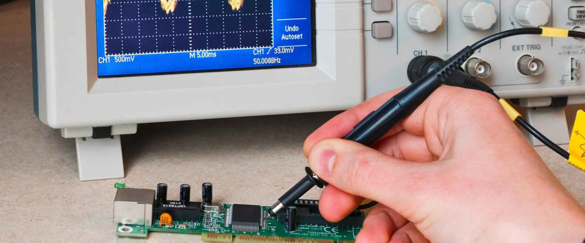
Test and Measurement Equipment:

The flexibility of FPGAs makes them ideal for implementing the advanced digital protocols and signal generation used in test instrumentation like oscilloscopes and network analyzers. Keysight is a major FPGA customer for test equipment.

This breakdown indicates data center, aerospace/defense, and communications represent the largest current market segments for FPGAs, while automotive and industrial are emerging high growth sectors.

Regional Market Size

Xilinx Zynq fpga
Xilinx Zynq fpga

Geographically, the Asia Pacific region accounted for the greatest share of FPGA revenue in 2019:

RegionEstimated Revenue Share
Asia Pacific~40%
North America~25%
Europe~20%
Rest of World~15%

China is the single biggest country market for FPGAs due to its massive electronics manufacturing base across communications infrastructure, consumer devices, industrial automation, aerospace and automotive. Other major Asia Pacific markets include Taiwan, South Korea, and Japan.

North America remains a significant region for FPGA consumption in aerospace/defense, data centers, and tech R&D. Top countries are the United States, Canada, and Mexico. Europe represents the third largest regional market led by Germany, France, and the United Kingdom.

As Asian countries continue rapid adoption of electronic systems and investment in high-tech research, the region will drive FPGA market growth in the coming decade.

Leading FPGA Companies

Below are profiles of the major FPGA suppliers comprising the market:

Xilinx

The leading global FPGA vendor with over 50% market share. They pioneered SRAM-based FPGA technology starting in the 1980s. Xilinx offers the broadest portfolio of FPGAs for applications from aerospace to data centers. Recently acquired by AMD.

Intel (Altera)

Intel entered the FPGA market after acquiring Altera in 2015. Altera was the second largest FPGA company behind Xilinx. Intel now offers FPGAs based on Altera technology targeted for data center acceleration.

Lattice Semiconductor

Lattice focuses on the low cost, low power FPGA market. Their โ€œvalue FPGAโ€ architecture is popular for consumer and industrial devices. Lattice claims the #1 market share for FPGAs under $15.

Microchip Technology

Microchip entered the FPGA market after acquiring Microsemi in 2018. Microsemi supplies radiation-tolerant FPGAs widely used in aerospace and defense systems.

QuickLogic

QuickLogic designs ultra-low power FPGAs aiming at mobile and IoT edge applications. Their โ€œsensing hubโ€ devices integrate sensor processing with analytics.

Achronix Semiconductor

Achronix is a private startup specializing in high-performance data center and networking FPGAs using an asynchronous “Speedster” architecture.

Xilinx and Intel together have over 80% FPGA market share. Smaller vendors like Lattice, Microchip, QuickLogic, and Achronix compete on specialized capabilities or emerging segments like low power edge devices.

Conclusion

In summary, the global FPGA market in 2019 was approximately $5 billion based on estimates from major analyst firms. Market growth is projected to accelerate over the next 5 years, with the industry forecast to reach $8 to $9 billion by 2025. This represents a strong 9-12% compound annual growth rate over the next several years.

Xilinx maintains dominance with 50%+ market share, trailed by Intel/Altera at 30-40% share. The Asia Pacific region currently represents the largest geographic market for FPGAs, while applications in data centers, aerospace/defense, and communications infrastructure are leading end-use segments. As adoption of FPGAs increases for AI acceleration, 5G, autonomous vehicles, Industry 4.0, and other leading-edge electronics, continued expansion of the FPGA market is expected through the next decade.

Frequently Asked Questions

xilinx-spartan-6-fpga-tutorial

What are the main factors driving growth in the FPGA market?

Key drivers expanding the FPGA market include:

  • Acceleration demands of AI, machine learning, and cloud computing
  • Development of 5G wireless infrastructure
  • Innovation in IoT, edge computing, and embedded devices
  • Advances in autonomous vehicles and ADAS capabilities
  • Aerospace/defense electronics sophistication
  • Rising complexity of chip designs requiring prototyping
  • Growth in broadband networks and high-speed communication

What are the challenges facing the FPGA industry?

Challenges for FPGA suppliers include:

  • Very high cost of developing new FPGA fabrication processes
  • Competition from ASICs for high volume production
  • Constant innovation required to match emerging standards
  • Migration of hardware acceleration functionality to custom AI chips
  • Geopolitical risks that can constrain access to major country markets

Who are the major customers for FPGAs?

Leading customers include:

  • Hyperscale data centers like Amazon, Microsoft, Baidu
  • Telecom infrastructure firms like Huawei, Nokia, Ericsson
  • Aerospace/defense contractors such as Lockheed Martin, Northrop Grumman, Boeing
  • Automotive companies including Tesla, Ford, GM
  • Test and measurement equipment vendors like Keysight, Tektronix
  • Government research organizations

What new capabilities are being added to FPGAs?

Emerging capabilities recently added to FPGAs include:

  • Integrated high-speed transceivers for 100G+ communication
  • Embedded ARM cores for hybrid FPGA-SoC architectures
  • Digital signal processing (DSP) blocks for speech recognition and vision algorithms
  • Hardened AI accelerators for neural network inferencing
  • Advanced package integration like 2.5D and chiplet designs
  • Multi-chip module approaches combining FPGA fabric with HBM memory

Who are the emerging FPGA startups to watch?

New startups bringing innovative architectures include:

  • Mythic – Using analog compute in place of digital logic
  • Symplectic – โ€œNeuromorphicโ€ devices mimicking brain structure
  • Wave Computing – Dataflow architecture optimized for AI
  • Leopard Imaging – Bringing FPGA technology to edge vision applications
  • FlexLogix – EFLX eFPGA IP for embedding logic in SoCs

How do you rework a BGA?

bga rework process

Introduction

Ball grid array (BGA) packages are increasingly used for integrated circuits and CPUs due to their high density interconnect capability. However, the underneath grid of solder ball connections also makes BGA chips very difficult to rework when faults occur. Proper BGA rework technique is essential to safely remove and replace BGAs without damage. This guide covers BGA rework fundamentals, the necessary tools, and step-by-step process instructions.

Overview of BGA Packages

BGA packages connect the IC to a PCB through an array of solder balls on the bottom of the package:

  • Dense grid arrays up to 35×35 mm package size
  • Pitch between balls as small as 0.5 mm
  • I/O counts over 1500 pins possible
  • Allows high speed routing on PCB top layer

However this interconnect method poses challenges for rework:

  • Solder balls are not easily accessible
  • Heating the entire BGA evenly is difficult
  • Mechanical shear force risks pad damage on removal
  • Precise alignment needed for replacement

Special BGA rework equipment and processes are required to address these challenges and successfully replace BGAs.

BGA Rework Equipment

YouTube video

The key pieces of equipment for professional BGA rework include:

BGA Rework Station

A dedicated rework station provides fine temperature control and tools for accessing underneath BGAs. Features include:

  • Bottom pre-heater to evenly heat the board from below
  • Top infrared heater and nozzle for local chip heating
  • Microscope for viewing the ball grid array during operation
  • Tweezers, spatulas, and pick-place tools for alignment

Soldering Station

A temperature-controlled soldering iron between 350-450ยฐC may be required for reballing and local touchup of solder joints. Fine tip sizes under 1 mm are preferable.

Solder Paste

SAC305 lead-free solder paste matched to the solder alloy on the board is required for reballing BGA pads.

Solder Balls

New solder balls with diameter and alloy matched to the BGA are necessary for reballing the package.

X-Ray Inspection

Post-rework x-ray imaging validates proper solder joint formation under the BGA.

BGA Rework Process Overview

The BGA rework process involves the following primary steps:

  1. Site Preparation – Cleaning, ESD protection, flux application
  2. Removal – Heating to reflow all solder joints, then lifting BGA
  3. Site Redressing – Cleaning pads, removing residue
  4. Reballing – Applying new solder balls using solder paste
  5. Replacement – Aligning and placing new BGA, reflowing in place
  6. Inspection – Visual and x-ray inspection of solder joints
  7. Testing – Electrical testing to validate proper function

Each phase requires care and the proper equipment to avoid damaging PCB pads, traces, or the replacement component.

Process Step 1: Site Preparation

Prior to removal, the site must be prepared:

  • Ensure ESD-safe environment – use wrist strap grounded to station.
  • Clean board thoroughly around the BGA area using isopropyl alcohol.
  • Apply liquid flux around the perimeter of the BGA onto the wetting surfaces. This aids heat transfer during reflow.
  • Secure board in rework station and calibrate optics.

Process Step 2: Removal

With flux applied, the BGA can be heated and removed:

  • Position preheating nozzle under board aligned with BGA center.
  • Set bottom side pre-heater to 150ยฐC and heat soak for 1-2 minutes to slowly warm board.
  • Position top side IR heating nozzle aligned to BGA center, approximately 1 mm above package.
  • Set top side heater temperature to 350ยฐC.
  • Close top heater nozzle and flood BGA with IR heat. Monitor temperature.
  • Keep heating until solder reflow temperature ~250ยฐC is achieved.
  • Hold at reflow temperature for 20-40 seconds for full joint liquefaction.
  • Raise top heating nozzle and use pick tool to slide BGA off site with gentle shear force.

Go slow during heating and lifting to prevent pad damage. Any remaining solder should stay on pads.

Process Step 3: Site Redressing

Once BGA is removed, the site must be cleaned for rework:

  • Use solder wick braid and flux to thoroughly clean pads, removing any solder residue.
  • Inspect pads under microscope to ensure no damage or lifting occurred.
  • If needed, use soldering iron at 350ยฐC to re-wet any lifted pads.
  • Clean off all remaining flux using isopropyl alcohol.

Process Step 4: Reballing

Next solder balls are replaced onto BGA pads:

  • Apply small dab of solder paste onto center of each pad using mini stencil or dispenser.
  • Use tweezers to place a new solder ball onto each paste deposit. Follow BGA ball layout pattern.
  • Ensure balls sit flat on paste and not on neighboring pads.
  • Once all sites reballed, use heating nozzle above 150ยฐC to gently tack balls in place without reflowing fully.

Process Step 5: Replacement

The new BGA can now be aligned and soldered:

  • Position BGA above site using pick tool and align fiducials.
  • Lower BGA onto pads slowly allowing self-centering with gentle downward force.
  • Inspect under microscope to confirm all solder balls making contact with paste deposits.
  • Apply flux around perimeter of BGA onto any visible solder.
  • Use heating nozzle to reflow attach the component using thermal profile up to 250ยฐC peak temperature.
  • Maintain heat until solder fully wets pads and reflow is complete.
  • Allow assembly to cool down before further handling.

Process Step 6: Inspection

Verify joint quality under BGA after replacement:

  • Visually inspect perimeter joints and look for proper fillet formation.
  • Use x-ray imaging to view hidden solder joints under package.
  • Confirm all joints are formed without shorts or opens.
  • Take high magnification photos documenting rework process if desired.

Process Step 7: Testing

bga-rework-machine

Functionally test board after BGA rework:

  • Perform in-circuit testing if fixture available.
  • Power up and exercise system functionality.
  • Run board self-test, diagnostics, or functional test routines if exist.
  • Retest any parameters out of specification before rework.
  • Document electrical test results.

Thorough inspection and testing is crucial to confirm a successful BGA rework.

BGA Rework Challenges

While following the fundamental rework process, there are some common challenges:

Residue Cleaning – Failed joints or charred flux residue under BGAs requires effort to clean entirely before reballing.

Pad Damage – Lifting BGAs risks tearing pads or traces, requiring soldering repairs.

Reballing Small Units – Precise paste deposition and ball placement is difficult for fine pitch < 0.8 mm BGAs.

Voiding – Entrapped air in solder joints under package due to incomplete wetting or flux boiloff.

Thermal Stress – Repeated high temperature exposures during removal and replacement can overheat board or adjacent components.

Proper training, fine tip tools, and extensive practice helps mitigate these challenges when reworking BGA packages.

Conclusion

Reworking BGA packages requires specialty heating equipment, precise soldering technique, and training to master the process. With practice, the majority of BGAs with 600 balls or less can be successfully reworked using suitable tools and diligence following the steps outlined here. Larger high-density BGAs may require outsourcing to an advanced rework facility. But for most common applications, understanding proper in-house BGA rework technique enables repair of these challenging packages.

Frequently Asked Questions

eMMC BGA

What key tools are required for BGA rework?

The essential tools include:

  • BGA rework station with split top/bottom heaters
  • Temperature-controlled soldering iron
  • Solder paste and solder balls matched to BGA
  • Solder wick, flux, picks, tweezers
  • Microscope for working under BGA
  • X-ray imaging capability

What size BGAs can be reasonably reworked by hand?

BGAs up to about 600 balls with 0.8 mm pitch can be reworked with practice using manual tools and optical magnification. Above ~35 x 35 mm size and 0.5 mm pitch requires more advanced rework equipment.

How can I avoid damaging pads when removing BGAs?

  • Keep board as cool as possible during BGA removal
  • Avoid excessive shear force when sliding off component
  • Use generous flux underneath to lower surface tension
  • Consider hot air tools instead of force to lift large BGAs

What is the most common defect seen in BGA rework?

Insufficient solder paste application prior to reballing typically results in unattached balls and unreliable solder joints after replacement BGA attachment. Generous paste volumes are key.

How can I validate successful BGA rework?

  • Detailed visual inspection around all ball joints
  • X-ray imaging to view hidden solder connections
  • Testing board electrically before and after rework
  • Running system diagnostics and functionality check

What is the difference between a flex circuit and a PCB?

quick turn flexible PCB prototype

Introduction

Printed circuit boards (PCBs) and flex circuits are common technologies used to interconnect electronic components and provide mechanical support. While both utilize conductive traces and pads on an insulating substrate, there are important differences between rigid PCBs and flexible circuits.

This article will examine the variations in materials, construction methods, performance capabilities, and typical applications for flex circuits versus PCBs. Understanding the tradeoffs involved can help designers select the optimal interconnection technology for each system.

PCB Overview

A printed circuit board consists of thin alternating layers of conductive copper and insulating dielectric substrate. The substrate material most commonly used is FR-4 fiberglass, which is rigid and relatively inexpensive. Other rigid laminate materials include FR-5, GETEK, and polyimide.

The board fabrication process generally includes:

  1. Drilling holes for component leads and vias
  2. Electroless copper plating to metallize the holes
  3. Laminating copper foil onto the substrate
  4. Photolithography to print the circuit pattern onto the copper
  5. Etching away unwanted copper to form isolated traces
  6. Applying protective solder mask over the traces
  7. Silkscreen printing of component designators

This subtractive process results in a rigid board with etched copper traces connecting surface mount and through-hole components soldered onto the pads. PCBs can be single, double, or multilayer with traces on both sides and internally between layers.

6 layer FR-4 PCB with surface mount and through-hole components

PCB Attributes:

  • Rigid fiberglass substrate
  • FR-4, FR-5, GETEK, polyimide, ceramic materials
  • Multilayer construction possible
  • High density interconnects
  • Fine line & space traces
  • Plated through hole vias
  • Lower cost process

Flex Circuit Overview

YouTube video

A flex circuit consists of conductive traces and pads on a flexible dielectric substrate material. This allows the circuit to bend and flex dynamically during use. Polyimide films like Kapton or UPILEX are commonly used as the flexible insulating base material.

There are two main methods for creating a flex circuit:

Additive: An additive process is typically used for finer features. Conductive material is selectively deposited onto the substrate through masking and electroplating:

  1. A thin metal foil is laminated onto the substrate.
  2. Photoresist is applied and imaged to define the circuit pattern.
  3. Exposed areas are electroplated to build up the conductor thickness.
  4. Photoresist is stripped away, leaving the plated traces on an etched foil base.

Subtractive: A subtractive process can also create flex circuits, removing unwanted copper similarly to rigid PCB fabrication:

  1. An adhesive layer bonds a copper foil to the flexible substrate.
  2. Photoresist is laminated and imaged with the circuit layout.
  3. Exposed copper is chemically etched away.
  4. The remaining photoresist is stripped off.
flex-circuit-manufacturer

Polyimide flex circuit fabricated with an additive process

Flex Circuit Attributes:

  • Thin flexible substrate
  • Polyimide, PEEK, PET, TPU, PEN materials
  • Difficult to make multilayer
  • Tighter trace routing density
  • Finer lines and spaces
  • Flexible adhesive connections
  • Requires special handling

Physical Construction Comparison

PCBs and flex circuits vary quite a bit in terms of their physical construction and materials used:

ParameterPCBFlex Circuit
SubstrateFR-4, G10, GETEK, BTPolyimide, PEEK, PET
Dielectric Thickness1.6mm, 2.4mm typical25ฮผm – 75ฮผm typical
LayersUp to 30+ layersTypically single layer or double layer
Conductor1oz – 3oz copper foil0.5oz – 2oz rolled annealed copper
Line Width100ฮผm minimum15ฮผm possible
Line Spacing150ฮผm minimum25ฮผm minimum
Via ConstructionPlated through holeMicrovias, filled vias
FlexibilityRigidDynamic flexing capability
WeightHeavierLighter weight

Some key differences to note:

  • PCB substrates are thicker for structural rigidity, while flex circuits use thin flexible polymer films.
  • Multilayer constructions are common with PCBs but challenging with flex circuits.
  • Flex circuits can achieve finer trace widths and pitches.
  • Flex circuits are inherently flexible for dynamic movement requirements.

Performance Comparison

Flexible pcb board cost

The design objectives and use environment drives the performance requirements for an interconnection technology. Here is how PCBs and flex circuits compare for some key parameters:

Electrical Properties

MetricPCBFlex Circuit
Dielectric ConstantFR4: 4.5Polyimide: 3.5
Loss TangentFR4: 0.017Polyimide: 0.003
Insulation Resistance100 Tฮฉ typical20 Tฮฉ typical
Breakdown Voltage23 kV/mm16 kV/mm
Propagation SpeedFR4: 60%Polyimide: 85%
  • Flex circuits generally have lower loss and higher frequency performance.
  • PCBs can operate at higher voltages.
  • Match dielectric materials to application signal frequencies.

Mechanical Properties

MetricPCBFlex Circuit
Young’s ModulusFR4: 20-30 GPaPolyimide: 2.5 GPa
Tensile StrengthFR4: 275 MPaPolyimide: 231 MPa
Flexural RigidityVery low flexibilityCan bend dynamically
Thermal ExpansionFR4: 12-16 ppm/CPolyimide: 20 ppm/C
  • PCBs are rigid with high stiffness.
  • Flex circuits are flexible but have lower strength.
  • Coefficient of thermal expansion varies.

Environmental Resistance

MetricPCBFlex Circuit
Flammability RatingFR4: V-0Polyimide: V-0
Moisture AbsorptionFR4: 0.2%Polyimide: 2.0%
Chemical ResistanceFair acrylics, alcoholsGood overall
UV TolerancePoor – yellowsExcellent UV stability
Operational TemperatureFR4: 130ยฐCPolyimide: 260ยฐC
  • Both meet flammability standards for electronics.
  • Polyimide has broad chemical resistance.
  • Flex circuits withstand higher temperatures.

PCB vs. Flex Circuit Layout Comparison

The different construction and capabilities of PCBs and flex circuits require adapted layout strategies.

For PCBs, common practices include:

  • Partitioning circuits across multiple rigid layers
  • Escape routing component leads with clearance for etch and drilling
  • Area fills for power and ground planes
  • Grid-based placement with fixed 90ยฐ routing
  • High density surface mount components on both sides
  • Matching trace widths to current requirements
  • Impedance control traces and serpentine length matching

Flex circuit layout is characterized by:

  • Constrained to 1-2 flexible layers
  • Tight component placement and routing density
  • Curved traces following substrate contours
  • Selective reinforcements and stiffeners
  • Avoiding 90ยฐ traces and joints during flexing
  • Adhesive openings to isolate rigid sections
  • Careful management of cross-section changes
  • Fabrication-aware keepout margins

These examples illustrate the differing approaches needed to optimize layouts.

Typical Applications

Due to their distinct properties, PCBs and flex circuits tend to be used in very different types of products and assemblies.

Common PCB Applications:

  • Computer motherboards and expansion cards
  • Consumer electronics like phones and tablets
  • Telecommunications infrastructure equipment
  • Automotive engine control units (ECUs)
  • Industrial control systems
  • Power electronic converters
  • LED lighting drivers

PCBs provide an inexpensive rigid interconnection foundation for electronic subsystems and complex digital circuits. The modular nature allows assembly and servicing of individual boards.

Common Flex Circuit Applications:

  • Printers and scanners
  • Computer disk drives
  • Robotic arms
  • Medical imaging equipment
  • Fitness trackers and wearables
  • Avionics systems
  • Automotive sensors
  • High temperature electronics

When dynamic flexing, tight space constraints, or projected lifetime motion cycles are involved, flex circuits can provide reliable interconnects without wires or connectors. The continuous constructions allows flex circuits to fit product industrial design needs.

Cost Considerations

For low volume, PCBs generally have a lower cost per unit compared to flex circuits. The reasons include:

  • Economies of scale with massive worldwide PCB production volumes
  • Lower cost raw materials like standard FR-4
  • Highly automated fabrication processes
  • Mature assembly ecosystems and acceptance testing

As production quantities scale, flex circuits can reach similar price points for an overall system. Other considerations like these can also impact cost:

  • Layer count – Multilayer PCBs get exponentially more expensive
  • Fabrication yield – Thin flex circuits can have more waste
  • Connectors avoided – Flex circuits eliminate these costs
  • Testing – Both require verification time and overhead
  • Serviceability – Repairing flex circuits may require full replacement

The optimal choice involves weighing production volume, system complexity, product lifecycle, and manufacturing strategy tradeoffs.

Hybrid PCB/Flex Applications

In some cases, combining rigid PCBs with flex circuits provides an ideal solution. Some examples include:

  • Hinge connections: Flex circuits folding around a corner or hinge to interconnect PCBs. Used extensively in flip phones and laptops.
  • Screen connections: Flexible circuits connecting a display or touchscreen behind a device cover to the main PCB. Allows full range of adjustability.
  • Sensor arrays: Flex circuits create dynamic conformal sensor grids that attach to rigid sensor hub PCBs. Used in robotic skin, building HVAC monitors, and body networks.
  • Wearables: A rigid PCB provides processing and wireless functions, while flex circuits interconnect across clothing and accessories. Seen in rings, watches, and fitness bands.
  • Printers: Flex circuits span the moving print head assembly while connecting to controller boards. Also used in cameras and scanners.

For these applications, flex circuits essentially act as 3D interconnects integrated with planar PCBs when needed.

Summary and Recommendations

Here are some best practices based on the PCB and flex circuit comparison:

  • Select PCBs for static rigid boards with multilayer needs or high voltage.
  • Use flex circuits when flexibility, tight space, or motion cycling are critical.
  • Combine both technologies in a system when needed for modular and dynamic functions.
  • Match dielectric material properties to required performance characteristics.
  • Account for fabrication yield, testing, and serviceability costs.
  • Adapt layout and component selection to the properties of each technology.
  • Seek expert guidance to ensure a reliable design optimized for manufacturability.

Understanding these fundamental differences between printed circuit boards and flex circuits allows designers to make informed tradeoffs and utilize each technology appropriately.

FQA

What are the main differences between flex circuits and rigid PCBs?

The main differences are the flexible substrate material, thinner dielectric layers, finer traces, and dynamic flex capability of flex circuits versus the rigid multilayer FR4 construction and lower cost of traditional PCBs.

Why choose a flex circuit over a PCB?

Use flex circuits when the application requires tight space constraints, dynamic motion and flexing, or conformal shape adaptation that rigid boards cannot provide.

What are some examples of typical flex circuit applications?

Common uses include printers, disk drives, robotic joints, medical equipment, wearables, avionics, and automotive sensors. The flex circuits can adapt to motion and space requirements that PCBs cannot.

What are some typical applications for conventional PCBs?

PCBs are well suited for computers, servers, telecom systems, control systems, LED lighting, and consumer electronics where rigid support for multilayer digital circuits is acceptable.

When does using both PCBs and flex circuits together make sense?

PCB and flex circuit hybrid assemblies provide advantages in applications like laptops, wearables, printers, and sensors that have both dynamic flexible interconnections and rigid support or multilayer circuit needs.

What is the best waterproof coating for electronics?

PCB Assembly conformal coating

Introduction

Why should the PCBA brush conformal coating

Electronic devices and components exposed to moisture, humidity, condensation, or direct water contact are susceptible to corrosion, electrical leakage, and reliability failures. Protecting circuits and assemblies with waterproof coatings and encapsulants is critical for applications where electronics will encounter wet environments.

But with the wide variety of waterproofing materials available, how do engineers choose the optimal protective coating? Key factors to consider include the application requirements, coating properties, material compatibility, application methods, and qualification testing.

This article provides a detailed overview of waterproof coating technologies for electronics along with guidance on selection criteria and best practices. With an understanding of the different coating options and their capabilities, designers can make informed decisions on implementing the best waterproofing protection regimes for their products.

Waterproofing Requirements

The first step is identifying the specific waterproofing needs based on the application and operating environment:

  • Liquid exposure: Will the electronics encounter direct water submersion, pressurized sprays, splashing, or only incidental moisture?
  • Duration: Is water exposure occasional and temporary, or continuous for extended periods?
  • Chemical compatibility: Does the coating need to withstand specific fluids like saltwater, acids, or hydrocarbon oils?
  • Temperature range: What are the temperature limits for material performance?
  • UV and abrasion: Will the coating experience wear, UV radiation, or chemical degradation factors?
  • Repairability: Does the application require repairable/reworkable waterproofing?
  • Electrical properties: Are dielectric strength, surface insulation, and other electrical properties important?
  • Application method: Can the coating be cast, brushed, sprayed, or dip applied?

With an understanding of the environmental stresses and product requirements, the waterproof coating type can be selected.

Coating Properties

YouTube video

There are a wide variety of waterproof electronics coatings that seal components and PCB assemblies from moisture ingress and corrosion. Here are key performance properties to consider when comparing options:

Solvent and Curing

  • Solvent-cured: Use evaporation and chemical reaction of solvents to harden coating after application.
  • UV-cured: Cure rapidly upon exposure to UV irradiation. Minimal solvents.
  • Heat-cured: Apply as liquid or paste, then cure with oven baking process.
  • Room temperature cure: Cure at room temperature using catalytic chemical reactions.

Permeability

  • Impermeable: Cannot be penetrated by water molecules. Provides highest reliability.
  • Conformal: Thin coats follow PCB topology but allow slow moisture diffusion. Reliance on isolation layers.
  • Permeable: Absorbs moisture but provides temporary water resistance. Used with venting strategies.

Thermal and Mechanical

  • Operating temperature: Upper limit before coating degrades, typically 120ยฐC to 230ยฐC.
  • Coefficient of thermal expansion (CTE): Match to substrate to reduce stress and delamination.
  • Hardness and mar resistance: Resists abrasion, nicks, cuts. Shore D 65-85 typical range.
  • Adhesion: Bond strength to substrate, measured in psi. 500 psi minimum recommended.
  • Flexibility: Ability to bend without cracking. Important for flex PCB applications.

Electrical

  • Dielectric strength: Voltage withstand rating, reported in V/mil. 500-1500 V/mil target.
  • Dielectric constant: Impacts impedance and capacitance for coating thickness. 2.5-4.0 typical.
  • Insulation resistance: Resistivity in ฮฉ or Tฮฉ reflecting conduction losses.
  • Dissipation factor: Dielectric losses from polar molecules under AC excitation. Lower is better.

Material Types

Some of the main classes of waterproof electronics coatings include:

Acrylics

  • Simple, low cost resin coatings
  • Fast room temperature cure
  • Medium hardness and flexibility
  • Moderate temperature rating
  • Easy application by dip, spray, or brush

Urethanes

  • Tough, abrasion resistant coatings
  • Single or two part chemistries
  • Temperature, UV, and chemical resistant
  • Excellent adhesion and flexibility
  • Can be rigid or rubber-like

Silicones

  • Inorganic silicone polymers
  • Very broad operating temperature range
  • Excellent moisture and UV resistance
  • Conformal thin film coats with high elasticity
  • Moderate dielectric strength

Epoxies

  • Strong adhesion and environmental resistance
  • Range of flexible to rigid coatings
  • Excellent dielectric properties
  • Withstand rugged use conditions
  • Room temperature or heat cure options

Parylenes

  • Unique vapor deposited polymer films
  • Extremely conformal thin coats
  • Superb dielectric strength and moisture barrier
  • Expensive process with high capital costs

This covers some of the major coating material types. Comparing options within each category based on specific needs is key.

Waterproof Coating Methods

PCBA Conformal Coating

There are several approaches to protect electronics from water exposure:

Conformal Coatings

Conformal coatings provide thin layers that follow the contours of components and PCBs. Common coating methods include:

  • Spray: Automated selective spray systems or manual aerosol cans deposit controlled coats.
  • Brush: Manual application allows selective brushing but can leave voids.
  • Dip: Full immersion followed by controlled withdrawal leaves a thin uniform coat.
  • Vapor deposition: Parylene coatings are applied as gaseous monomers that polymerize onto surfaces.

Typical conformal coat thickness ranges from 25-75 ฮผm. While offering some water resistance, conformal coats rely on the PCB soldermask layer as the primary water barrier.

Conformal epoxy coating applied over PCB assembly

Potting Compounds

Potting fills the entire electronics enclosure with a thick protective resin encapsulant:

  • Casting: Liquid resins poured or injected then cured to harden
  • Compression: Potting compounds compressed around components
  • Impregnation: Vacuum draws resin into complex assemblies

Typical potting thickness from 2mm up to 25mm. Provides excellent water resistance but limits access for rework.

Electronic device encapsulated with thick potting material

Sealed Housing

For the most critical applications, electronics can be entirely sealed within a watertight enclosure:

  • Plastic or metallic housings: O-ring or gasket sealed, often with added potting material
  • Hermetic housings: Use welded or soldered metal enclosure with added desiccant to maintain <1% internal humidity

This provides protection for continual or extreme submersion but with higher cost. Regular seal inspection and maintenance may be required. Accessing internals becomes difficult.

Electronics assembly sealed within a hermetic metal enclosure

Selection Criteria

PCB-circuit-board-waterproof-coating

Choosing an optimal waterproofing approach requires tradeoffs across many factors:

Exposure Level

  • For temporary moisture or rain exposure, conformal coating provides adequate protection.
  • Applications with prolonged submersion will require potting material or a fully sealed housing.

Mechanical Properties

  • Conformal coats maintain flexibility for dynamic components and flex PCBs.
  • Brittle potting compounds require fixed rigid support.

Thermal Properties

  • Conformal coats allow convection and air cooling of electronics.
  • Thick potting compounds act as a thermal insulator requiring other cooling methods.

Electrical Performance

  • Conformal coats have limited dielectric strength and higher capacitance.
  • Potting better withstands voltage exposures but may require insulation displacement.

Repairability

  • Conformal coats can be selectively reapplied after rework.
  • Encapsulants prevent access to components without full removal.

Weight

  • Thin conformal coats minimize weight impact.
  • Dense potting resins increase weight, which may be prohibitive.

Cost

  • Adding conformal coat has lower material cost but process impact.
  • Potting resins and sealed housings have higher material expense.

With an understanding of these considerations against application requirements, the optimal coating method can be selected.

Qualification Testing

Verifying a chosen waterproof coating will meet product reliability requirements under real-world conditions is critical. Typical qualification tests include:

Coating Cure Validation

  • Measure shore hardness to confirm full cure
  • Exposure to excess working time to check for tackiness or soft spots
  • Thermal shock or rapid temperature ramping
  • Sample cross-sectioning to validate uniform cure

Adhesion Testing

  • ASTM D3359 crosshatch tape tests
  • Initial adhesion and after thermal cycling
  • Pull-off adhesion tests before and after liquid exposure

Electrical Properties

  • Dielectric breakdown voltage
  • Insulation resistance
  • Combing resistance under bias voltage
  • Capacitance changes from coating

Fluid Exposure

  • Salt spray fog per ASTM B117 standard
  • Thermal shock and moisture cycling
  • Water submersion and chemical compatibility
  • Flammability testing after exposure

The specific test conditions and performance requirements will depend on the product specifications and reliability models. But following a thorough qualification protocol matched to application conditions ensures the coating will function as needed.

Application Best Practices

Conformal Coating
Conformal Coating

Properly applying waterproof electronics coatings is vital for achieving protection. Key guidelines include:

Surface Preparation

  • Ensure PCBs are clean and dry before coating
  • Remove contaminants like rosin residue
  • Lightly abrade glossy soldermask
  • Apply adhesion promoter if needed

Process Controls

  • Maintain ambient conditions like temperature and humidity
  • Use clean tools dedicated for coating
  • Have proper PPE and ventilation
  • Carefully measure mixing ratios for multi-part coats

Coverage Assurance

  • Mask connectors or test points to avoid coating
  • Ensure full coverage on all components and PCB edges
  • Apply multiple coats for thick buildup if needed

Curing

  • Gradually ramp oven temperature for heat cure coatings
  • For UV cures, match wavelength to coating reaction
  • Validate full cure with testing before proceeding

Coating Repair

  • Spot repair thin coats rather than full removal
  • Have contingency plan for thicker encapsulant removal
  • Plan accessibility provisions into design

Adhering to structured processes ensures the chosen coating consistently provides reliable waterproofing protection.

Summary

Protecting electronic products from water exposure threats requires selecting the optimal protective coating for the specific application conditions and requirements. Key takeaways include:

  • Carefully consider liquid exposure levels, coatings properties, material compatibility, reparability needs, and other criteria.
  • Determine if thin conformal coating, thick potting encapsulant, or sealed housing provides the right level of protection.
  • Match candidate coatings to physical, electrical, and environmental reliability requirements.
  • Qualify top coating options with standards-based testing tailored to end use stresses.
  • Follow robust process controls and best practices during coating application.

By understanding the wide range of waterproofing options and how to select the best fit, engineers can implement effective water protection regimes for electronics operating in wet environments.

FQA

What are some typical applications requiring waterproof coatings on electronics?

Typical applications are outdoor equipment, marine electronics, automotive systems, appliances, IoT sensors, medical devices, industrial controls in washdown environments, and consumer electronics where liquid resistance is valued.

When is it preferable to use a thick potting encapsulant versus a thin conformal coating?

Potting makes sense for full submersion applications where conformal coats would allow moisture diffusion over time. Use thin coats when flexibility, repairability, weight impact, or thermal dissipation are critical.

What electrical factors should be considered when selecting a waterproof coating?

Key electrical factors are dielectric breakdown voltage rating, insulation resistance, dielectric constant, dissipation factor, and surface resistivity. Match coating properties to PCB layout clearances and any high voltage exposures.

How is a waterproof coating qualified for use in a particular product?

Typical qualification steps are evaluating coating cure consistency, verifying adhesion strength before and after reliability testing, measuring electrical properties, and exposing samples to simulated end use environments like salt fog or liquid submersion.

What are some best practice guidelines for applying waterproof electronics coatings reliably?

Best practices include proper surface preparation, process controls on ambient conditions and mixing, full coverage verification, controlled ramps for heat cures, validating full cure prior to further assembly, and having repair contingencies planned for.

Ceramic PCB Technology: A Complete Guide to Materials, Manufacturing, and Applications

Are you looking to understand the cutting-edge world of Ceramic PCBs? Youโ€™ve come to the right place. In this comprehensive guide, weโ€™ll explore everything you need to know about Ceramic PCB technology, from its basic structure to advanced manufacturing processes and applications.

What is a Ceramic PCB?

A Ceramic PCB, or Ceramic Printed Circuit Board, is a specialized type of circuit board that uses ceramic materials as its base substrate. Unlike traditional FR4 PCBs, Ceramic PCBs are designed to operate in harsh environments and high-temperature conditions where other PCBs would fail.

These innovative PCBs offer superior thermal management, excellent electrical insulation, and remarkable stability under extreme conditions. As a result, Ceramic PCBs are ideal for applications in aerospace, automotive,ย military, and other high-reliability sectors where performance under stress is critical.

The Structure of Ceramic PCBs

To truly appreciate the capabilities of Ceramic PCBs, it’s essential to understand their structure. Let’s break down the key components:

Ceramic Material

The foundation of a Ceramic PCB is its ceramic substrate. This material forms the base upon which all other components are built. The choice of ceramic significantly influences the PCB’s performance characteristics.

Conductors

Conductive layers, typically made of copper or other highly conductive metals, are applied to the ceramic substrate. These layers form the circuits and pathways for electrical signals.

Maximum Use Temperatures

One of the standout features of Ceramic PCBs is their ability to withstand high temperatures. Depending on the specific ceramic material used, these PCBs can operate at temperatures ranging from 150ยฐC to over 1000ยฐC.

Thermal Conductivity

Ceramic PCBs excel in heat dissipation, a crucial factor in high-power applications. The thermal conductivity of ceramic materials used in PCBs can range from 20 W/mK to over 200 W/mK, far surpassing traditional FR4 boards.

Breakdown Voltage

The high dielectric strength of ceramic materials results in excellent electrical insulation properties. Ceramic PCBs typically have breakdown voltages ranging from 10 kV/mm to over 20 kV/mm, depending on the specific ceramic material used.

Ceramic PCB Engineering Calculator
RayPCB Engineering Tools โ€“ Design, Analyze & Optimize Ceramic Circuit Boards
โŠž Select Ceramic Substrate Material
โœ“
Alumina (96%)
Alโ‚‚Oโ‚ƒ
Thermal Cond.
24-28 W/mK
Dielectric
9.8
CTE
7.1 ppm/ยฐC
Max Temp
1600ยฐC
Alumina (99.6%)
Alโ‚‚Oโ‚ƒ
Thermal Cond.
28-35 W/mK
Dielectric
9.9
CTE
7.4 ppm/ยฐC
Max Temp
1700ยฐC
Aluminum Nitride
AlN
Thermal Cond.
170-230 W/mK
Dielectric
8.8
CTE
4.5 ppm/ยฐC
Max Temp
1000ยฐC
Silicon Nitride
Siโ‚ƒNโ‚„
Thermal Cond.
70-90 W/mK
Dielectric
8.0
CTE
2.7 ppm/ยฐC
Max Temp
1200ยฐC
Beryllium Oxide
BeO
Thermal Cond.
250-300 W/mK
Dielectric
6.7
CTE
7.5 ppm/ยฐC
Max Temp
1800ยฐC
Zirconia
ZrOโ‚‚
Thermal Cond.
2-3 W/mK
Dielectric
25
CTE
10.5 ppm/ยฐC
Max Temp
2000ยฐC
โ„น๏ธ Material Selection Guide
Alโ‚‚Oโ‚ƒ (Alumina): Most cost-effective, ideal for general applications.
AlN: Best thermal performance, excellent for high-power LEDs and RF.
Siโ‚ƒNโ‚„: Superior mechanical strength, best for thermal cycling reliability.
BeO: Highest thermal conductivity but requires special handling (toxic dust).
ZrOโ‚‚: Excellent for high-temperature sensors and fuel cells.
Material Comparison Table
Property Alโ‚‚Oโ‚ƒ 96% Alโ‚‚Oโ‚ƒ 99.6% AlN Siโ‚ƒNโ‚„ BeO
Thermal Conductivity (W/mK) 24-28 28-35 170-230 70-90 250-300
Dielectric Constant (1MHz) 9.8 9.9 8.8 8.0 6.7
Flexural Strength (MPa) 350 400 350 700 230
Relative Cost LOW LOW-MED HIGH HIGH VERY HIGH

Materials Used in a Ceramic PCB

1050c ceramic board
1050c ceramic board

The choice of ceramic material is pivotal in determining the PCB’s performance characteristics. Let’s explore some of the most common materials used in Ceramic PCBs:

Aluminum Oxide (Alโ‚‚Oโ‚ƒ)

Aluminum Oxide, also known as Alumina, is one of the most widely used ceramic materials in PCB manufacturing. It offers:

  • Excellent electrical insulation
  • Good thermal conductivity (20-30 W/mK)
  • High mechanical strength
  • Cost-effectiveness compared to other ceramic options

Aluminum Nitride (AIN)

Aluminum Nitride is prized for its exceptional thermal properties:

  • Very high thermal conductivity (170-200 W/mK)
  • Excellent electrical insulation
  • Low thermal expansion coefficient
  • Suitable for high-power applications

Beryllium Oxide (BeO)

Beryllium Oxide offers outstanding thermal performance:

  • Extremely high thermal conductivity (270-300 W/mK)
  • Excellent electrical insulation
  • High thermal shock resistance
  • Note: BeO is toxic when inhaled as dust, requiring special handling precautions

Silicon Carbide (SiC) Ceramic PCB

Silicon Carbide is known for its robustness:

  • High thermal conductivity (120-270 W/mK)
  • Excellent mechanical strength
  • High temperature resistance
  • Suitable for harsh environment applications

Hybrid Ceramic

Hybrid ceramic materials combine different ceramic types or ceramics with other materials to achieve specific performance characteristics. These can be tailored to meet unique application requirements.

Types of Ceramic PCBs

Ceramic PCBs come in various types, each designed for specific applications and manufacturing processes. Here are some of the most common types:

  1. High Temperature Ceramic PCBs
  2. Low Temperature Ceramic PCBs
  3. Thick Film Ceramic PCBs
  4. Direct Bonded Copper (DBC) PCBs
  5. Direct Plate Copper (DPC) PCBs
  6. Low-Temperature Co-Fired Ceramic (LTCC) PCBs
  7. High-Temperature Co-Fired Ceramic (HTCC) PCBs
  8. Multi-Layered Ceramic PCBs
  9. LAM (Laser Activation Metallization) PCBs

Each type has its unique advantages and is suited for different applications. For instance, High Temperature Ceramic PCBs are perfect for aerospace applications, while LTCC PCBs are ideal for high-frequency applications in telecommunications.

Characteristics of Ceramic PCBs

Ceramic PCBs boast a unique set of characteristics that set them apart from traditional PCB materials. Some of these include:

  1. High temperature tolerance
  2. High thermal conductivity
  3. Material stability
  4. Excellent insulation performance
  5. Good corrosion resistance
  6. High surface hardness
  7. High compression strength
  8. High dielectric strength
  9. High breakdown voltage
  10. No water absorption
  11. Low loss at high frequencies
  12. Free of organic constituents
  13. High density assembly capabilities

These characteristics make Ceramic PCBs ideal for a wide range of demanding applications where traditional PCBs would fall short.

Design Considerations for Ceramic PCBs

When designing Ceramic PCBs, there are several important factors to consider:

  1. Thermal management
  2. Material selection
  3. Layer stack-up
  4. Via design
  5. Coefficient of Thermal Expansion (CTE)
  6. Signal integrity
  7. Manufacturing process compatibility

By carefully considering these factors, designers can create Ceramic PCBs that fully leverage the unique properties of ceramic materials.

Applications of Ceramic PCBs

Ceramic PCBs find applications in a wide range of industries and products. Some common applications include:

  1. Memory modules
  2. Receiving and transmission modules
  3. High-power electronic modules
  4. Electric power transmitters
  5. Semiconductor coolers
  6. High-power LED lighting
  7. Communication antennas
  8. Automotive sensors

From aerospace to automotive, Ceramic PCBs are enabling new possibilities in electronics design and performance.

Ceramic PCB vs. FR4 and MCPCB

Ceramic PCB Thermal Conductivity

To fully appreciate the advantages of Ceramic PCBs, it’s helpful to compare them with other common PCB types:

Ceramic PCB vs FR4 PCB

  • Material: Ceramic vs. fiberglass-reinforced epoxy
  • Thermal conductivity: Much higher in Ceramic PCBs
  • Temperature resistance: Significantly higher in Ceramic PCBs
  • Cost: Ceramic PCBs are generally more expensive

Ceramic PCB vs MCPCB

  • Material: Ceramic vs. metal core with dielectric layer
  • Electrical insulation: Generally better in Ceramic PCBs
  • Temperature resistance: Higher in Ceramic PCBs
  • Applications: Ceramic PCBs are more suited for extreme environments

Manufacturing Process of Ceramic PCBs

S/M Expose Machine

The manufacturing process of Ceramic PCBs involves several complex steps:

  1. Design and layout
  2. Substrate preparation
  3. Layer preparation (for multilayer PCBs)
  4. Conductive layer deposition
  5. Via drilling and filling
  6. Firing or sintering
  7. Additional layering (for multilayer PCBs)
  8. Component attachment
  9. Testing and inspection
  10. Finishing and coating
  11. Final testing
  12. Packaging and delivery

Each step requires precision and expertise to ensure the final product meets the high standards required for Ceramic PCBs.

Choosing the Right Ceramic PCB Production Company

Selecting the right manufacturer for your Ceramic PCBs is crucial. Consider factors such as:

  1. Experience in Ceramic PCB manufacturing
  2. Technical capabilities
  3. Quality control processes
  4. Industry certifications
  5. Technical support
  6. Prototyping and volume production capabilities
  7. Cost-effectiveness
  8. Lead times
  9. Environmental compliance
  10. Customer references

By carefully evaluating these factors, you can choose a manufacturer that will deliver high-quality Ceramic PCBs that meet your specific needs.

Conclusion

Ceramic PCBs represent a significant advancement in PCB technology, offering unparalleled performance in extreme conditions. As electronics continue to push the boundaries of what’s possible, Ceramic PCBs will play an increasingly important role in enabling new applications and innovations across various industries.

By understanding the materials, types, characteristics, and manufacturing processes involved in Ceramic PCBs, engineers and designers can leverage this technology to create more robust, efficient, and reliable electronic systems. Whether you’re working in aerospace, automotive, telecommunications, or any other high-performance sector, Ceramic PCBs offer a solution that can meet your most demanding requirements.

Are you ready to explore how Ceramic PCBs can revolutionize your electronic designs? Start by identifying your specific needs and consulting with experienced Ceramic PCB manufacturers. With the right approach, you can harness the power of Ceramic PCB technology to take your projects to new heights of performance and reliability.

ย 

Rayming’s Electronic Laboratory: Ensuring PCBA Assembly Quality

RayMing has maintained a fully equipped Electronic Laboratory since 2017, dedicated to ensuring exceptional quality for all PCBA projects. Every circuit board assembly undergoes comprehensive testing in our facility before shipment to customers, guaranteeing reliability and performance.

For customers engaged in R&D projects, we extend access to our laboratory facilities to verify PCB designs. Our experienced engineers are available to provide technical assistance and testing support throughout your development process.

We conduct thorough verification including functional testing, environmental simulation, and reliability assessment to identify potential issues before they impact your product deployment. Our commitment to quality is reflected in our continuous investment in advanced testing equipment and expanding our capabilities to meet evolving industry requirements.

Partner with RayMing for peace of mind knowing your electronic assemblies have been rigorously validated by our dedicated testing professionals using industry-leading equipment and methodologies.

Customer use lab to test him products
PCBA Test machine
PCBA Test machine
Electronic Lab
Electronic Lab
X-RAY Test
X-RAY Test
SMT AOI
SMT AOI
pcba The first sample testing
PCBA Function test
PCBA Function test
Eletronic Test machine

Foundation of an Electronic Laboratory for PCBA Quality Assurance

Creating an effective electronic laboratory requires careful planning and implementation. The facility should feature anti-static flooring, controlled environmental conditions (temperature, humidity, and air quality), and sufficient lighting for detailed inspection work. The laboratory layout should follow the logical progression of the PCBA testing workflow, with dedicated zones for incoming component inspection, in-process testing, functional verification, reliability testing, and failure analysis.

This thoughtful organization minimizes cross-contamination risks while optimizing the efficiency of testing procedures. Additionally, the laboratory should include secure storage areas for reference boards, test fixtures, and documentation to maintain testing consistency over time.

Essential Equipment for Comprehensive PCBA Testing

Automated Optical Inspection (AOI) Systems

AOI systems use high-resolution cameras and sophisticated algorithms to detect visual defects such as missing components, incorrect polarity, misalignment, insufficient solder, or solder bridges. Modern AOI systems can capture 3D images to evaluate solder joint quality and component positioning with micrometer precision.

X-Ray Inspection Systems

X-ray inspection allows technicians to examine hidden solder joints beneath ball grid array (BGA) components, quad flat no-leads (QFN) packages, and other complex surface-mount devices. This non-destructive testing reveals voids, insufficient wetting, and internal structural defects that would otherwise remain undetected.

In-Circuit Test (ICT) Systems

ICT equipment uses a “bed of nails” fixture to make contact with test points on the PCBA, measuring electrical parameters and verifying component values against specified tolerances. This testing detects assembly errors, component failures, and manufacturing defects before functional testing begins.

Functional Test Equipment

Custom-designed functional testers simulate the operating conditions of the final product, verifying that the PCBA performs according to specifications. These systems can include power supply testing, signal generation, automated measurements, and software-driven test sequences that thoroughly exercise the circuit’s functionality.

Environmental Testing Chambers

PCBA reliability depends on performance across various environmental conditions. Temperature cycling chambers, humidity testing equipment, and vibration testing platforms subject assemblies to accelerated stress conditions, identifying potential weaknesses before they manifest in the field.

Solderability and Surface Analysis Tools

Specialized equipment for evaluating solder joint quality, surface cleanliness, and conformal coating integrity helps ensure long-term reliability. These tools can include dye penetrant testing apparatus, ionic contamination testers, and coating thickness measurement devices.

Failure Analysis Equipment

When defects occur, identifying root causes requires sophisticated analytical tools. Cross-sectioning equipment, scanning electron microscopes, thermal imaging cameras, and specialized probing stations enable technicians to isolate and characterize failure mechanisms at the component or board level.

Establishing Comprehensive Testing Protocols

A robust quality assurance system requires well-documented testing procedures that align with industry standards such as IPC-A-610 (Acceptability of Electronic Assemblies) and J-STD-001 (Requirements for Soldered Electrical and Electronic Assemblies).

These protocols should specify:

  • Sampling methodologies based on production volume and criticality
  • Detailed test sequences and procedures for each product type
  • Clear pass/fail criteria with measurable parameters
  • Documentation requirements and data retention policies
  • Handling procedures for non-conforming assemblies
  • Escalation pathways for recurring issues

Technical Expertise and Staff Development

The effectiveness of an electronic laboratory depends largely on the knowledge and skills of its personnel. Rayming should invest in:

  • Comprehensive training programs covering equipment operation, testing methodologies, and quality standards
  • Regular certification of testing technicians through industry-recognized programs
  • Cross-training to ensure operational flexibility and knowledge sharing
  • Continuing education to keep pace with evolving technologies and testing methods
  • Collaboration with engineering teams to improve both testing procedures and product designs

Data Collection and Statistical Process Control

Modern electronic laboratories implement sophisticated data management systems that capture testing results, track trends, and generate actionable insights. These systems enable:

  • Real-time monitoring of assembly quality metrics
  • Early detection of process drift before failures occur
  • Correlation analysis between defect types and specific production factors
  • Documentation for customer and regulatory requirements
  • Statistical process control implementation to maintain consistent quality

Integration with Production Processes

The electronic laboratory should not function in isolation but rather as an integral part of the manufacturing ecosystem. This integration requires:

  • Regular feedback loops between testing results and production processes
  • Collaborative problem-solving sessions involving laboratory technicians, process engineers, and production staff
  • Implementation of preventive and corrective actions based on testing data
  • Validation of process improvements through targeted testing
  • Development of new testing methodologies as product complexity evolves

Calibration and Measurement System Analysis

To ensure testing accuracy, all laboratory equipment must undergo regular calibration and validation. A comprehensive program should include:

  • Scheduled calibration against traceable standards
  • Gauge repeatability and reproducibility (GR&R) studies to validate measurement systems
  • Preventative maintenance schedules for all critical equipment
  • Validation of test fixtures against known reference assemblies
  • Documentation of all calibration activities and measurement system analyses

Customer-Specific Requirements Management

Different customers and industries often impose specialized testing requirements. The laboratory must remain adaptable to accommodate these variations while maintaining operational efficiency. This flexibility may necessitate:

  • Customer-specific test fixtures and procedures
  • Additional verification steps for critical applications
  • Enhanced documentation for regulated industries
  • Specialized reliability testing for harsh environment applications
  • Capability to implement new testing technologies as customer needs evolve

Conclusion

Establishing a comprehensive electronic laboratory represents a significant but essential investment for Rayming to ensure PCBA assembly quality. Beyond simply identifying defects, this facility serves as a central knowledge repository that drives continuous improvement throughout the manufacturing process.

By implementing advanced testing capabilities, rigorous protocols, and fostering collaboration between quality assurance and production teams, Rayming can differentiate itself in the competitive electronics manufacturing marketplace. As electronic products continue to increase in complexity and miniaturization, while reliability expectations remain stringent, a well-equipped electronic laboratory becomes increasingly critical to manufacturing success.

Through thoughtful planning, appropriate technology investment, thorough staff development, and seamless integration with broader manufacturing operations, Rayming’s electronic laboratory becomes not just a quality checkpoint but a strategic competitive advantage that delivers measurable value to customers through superior PCBA quality and reliability.

What machine is required for PCB Assembly?

smt assembly equipment
SMT Assembly Capacity

Introduction

Printed circuit board (PCB) assembly is the process of soldering electronic components to a PCB. This allows the creation of a functional electronic circuit. There are various machines and equipment used in PCB assembly to automate the production process. The main machines include soldering machines, inspection machines, material handling equipment, cleaning equipment and more.

Selecting the right PCB assembly equipment is crucial to achieving high productivity, quality and yield. The choice of machine depends on factors like:

  • Type of components to be soldered
  • Production volume
  • Required precision and accuracy
  • Budget

This article provides a comprehensive overview of the different types of machines used in PCB assembly and discusses their features, working principles, advantages and typical applications.

Soldering Machines

Soldering is the most important step in PCB assembly. It involves melting solder to create permanent joints between component leads and PCB pads. The main types of soldering machines are:

Wave Soldering Machine

A wave soldering machine passes the underside of the PCB over a wave of molten solder to simultaneously solder all solder pads and component leads. The key components are:

  • Solder pot – Contains molten solder alloy
  • Pump – Generates the solder wave
  • Preheating stage – Preheats the PCB to ensure proper soldering
  • Fluxer – Applies flux to PCB before soldering
  • Conveyor – Transports PCB through the machine

Wave soldering is ideal for soldering through-hole components on mass production PCBs. It allows high throughput up to thousands of boards per hour. However, it is not suitable for soldering surface mount devices (SMDs).

Reflow Soldering Oven

A reflow soldering oven uses heat to melt solder paste and form solder joints between SMDs and PCB pads. The oven has multiple heating zones with increasing temperatures to heat up the board. The stages are:

  • Preheating – Slowly heats up the board to evaporate solvents from solder paste
  • Reflow – Heats the board above the melting point of solder to form joint
  • Cooling – Cools the board down to solidify solder

For small volumes, reflow ovens with infrared heating are used. For mass production, convection ovens with forced air circulation provide faster heating. The peak temperature is around 217ยฐC.

Reflow ovens allow excellent soldering quality and are ideal for SMD assembly. However, cycle times are longer compared to wave soldering.

Selective Soldering Machine

A selective soldering machine solders specific parts on the board using a miniature solder wave or solder fountain. It has a solder pot, pump, fluxer and conveyor. The key difference from wave soldering is:

  • Soldering head – A precision soldering nozzle that selectively applies solder only where needed.

Selective soldering provides flexibility to solder both through-hole and SMD components. It is ideal for manual rework or soldering heat-sensitive components after reflow.

Inspection Machines

Inspection of solder joints and checking for defects is vital in PCB assembly. Common inspection machines include:

Automated Optical Inspection (AOI)

AOI machines use high resolution cameras to visually inspect the quality of solder joints. They use pattern recognition software to compare the PCB to a known good reference.

AOI provides fast and accurate inspection immediately after soldering. Both solder joints and component placement can be checked. However, it may not detect subtle flaws.

X-Ray Inspection

X-ray inspection uses X-ray imaging to see inside a PCB and inspect component soldering, placement and orientation. It creates a 3D image through the board, revealing hidden or buried defects.

X-ray inspection provides very detailed inspection. However, the equipment is more expensive than AOI. It is better suited for small boards.

Flying Probe Tester

This machine uses two movable “flying” probes to electrically test PCBs for shorts, opens, resistance and functionality. The probes move over the board and make contact with test points.

Flying probe testing verifies PCB assembly and detects manufacturing defects. It replaces fixture-based testing for small volumes.

Material Handling Equipment

Efficient material handling improves productivity in PCB assembly. Common material handling equipment includes:

Conveyor System

Conveyors are used to automatically transport PCBs between different assembly machines. This avoids manual material handling.

Automatic Solder Paste Printer

This machine uses stencils to apply the solder paste pattern onto the PCB before reflow soldering. It improves repeatability and reduces application defects.

Automatic Component Placer

This rapidly picks components from feeders and accurately places them on defined positions on the board. It avoids manual placement and improves quality.

Cleaning Equipment

After soldering, flux residue remains on the PCB which can be corrosive and conductive. Cleaning is essential. Common cleaning equipment:

Washers

Washers use liquids like deionized water to remove flux and other contaminants from the PCB surface. Different types include batch washers, inline washers, ultrasonic washers etc.

Cleaning Agents

Specialized cleaning agents like alcohols, solvents and detergents are used for effective PCB cleaning prior to washing.

Dryers

Dryers like centrifugal dryers are used to completely dry the PCB after washing to avoid any residual moisture.

Rework Equipment

Manual rework stations may be needed to repair defective boards or replace components. This allows recovery of PCBs instead of scrapping them. Common rework equipment includes:

Soldering & Desoldering Stations

Manual soldering/desoldering tools allow localised repair of solder joints without affecting the complete board. Hot air jets, infrared preheaters and vacuums ease the rework.

Fume Extraction Systems

Fume extractors remove harmful flux fumes released during rework soldering/desoldering. This improves operator safety.

ESD Control Equipment

Handling electronic components demands precautions against electrostatic discharge (ESD) which can damage sensitive devices. Common ESD control equipment:

Wrist Straps

Wrist straps ground the operator to safely discharge any static buildup.

ESD Mats

Conductive mats prevent electrostatic charge generation during handling and assembly.

Ionisers

Ionizers neutralize electrostatic charges by emitting positive and negative ions in the surroundings.

ESD Containers & Packaging

Components are stored and transported in static shielding bags and ESD certified containers.

Auxiliary Equipment

Some other auxiliary equipment required:

  • Storage racks for PCBs, components and materials
  • Workbench, chairs and tools for manual workstation
  • Solder wire, solder bars, fluxes, cleaning agents
  • Computer and software for production monitoring
  • Label printer for product identification
  • Measurement & testing equipment (microscopes etc.)
  • Fire extinguisher, first aid kit & PPE

Factors for Selecting PCB Assembly Equipment

The main factors guiding PCB assembly machine selection:

Throughput Rate

The production rate or number of boards that can be processed per hour. High throughput equipment like wave soldering and placement machines are needed for mass production.

Board Size

The dimensions of the PCBs being assembled. Large boards will need wider conveyors and large ovens.

Component Types

Through-hole, SMD or mixed? The component package types impact the soldering methods required.

Accuracy & Repeatability

Precision assembly demands machines with high accuracy, precision placement and consistent process control.

Multi-Product Versatility

Flexibility to switch between different PCB products, varying placement programs etc improves utilization.

Cost

Both equipment purchase cost and ongoing operating costs should be affordable.

Available Space

The floor space available in the production facility for accommodating the machines.

Operator Skill Level

Automated machines reduce dependency on operator skills. But rework still needs skilled operators.

Recommended Basic Setup

A basic setup for low volume PCB assembly could include:

  • Reflow oven for SMD soldering
  • Selective soldering machine for THD components
  • Automatic solder paste printer
  • Small component placement machine
  • AOI inspection system
  • Cleaning equipment like washer, dryer etc.
  • Rework station with microscope
  • Fume extraction system
  • ESD control equipment
  • Conveyor system for material handling

Whereas a setup for high volume manufacturing would include:

  • Wave soldering machine
  • Large reflow oven
  • High speed component placer
  • 2-3 AOI machines (pre-reflow and post-wave)
  • X-ray inspection system
  • Industrial washing systems
  • Automatic storage & retrieval systems
  • Extensive conveyor links between machines
  • Testing systems & flying probers

Main Suppliers of PCB Assembly Equipment

Some leading global suppliers of PCB assembly equipment include:

  • ASM – SMT placement, soldering and inspection systems
  • Juki – SMT assembling machines (placers, printers etc.)
  • Yamaha – Surface mount machines, bonders, printers
  • Panasonic – SMT production solutions
  • Europlacer – High speed, high precision component placers
  • Mycronic – Dispensing, jetting, placement and AOI
  • Nordson – Soldering (selective, wave) and dispensing systems
  • Vitronics Soltec – Wave and selective soldering machines
  • Asscon – Soldering machines (reflow, wave, selective)
  • Zymet – SMT screen printers, dispensers and placers
  • Manncorp – Reflow ovens,selective soldering and more
  • CTC – Conveyor systems for SMT production lines
  • Aqueous Technologies – PCB cleaning equipment
  • MPI – Automated optical inspection (AOI) machines
  • Viscom – 3D AOI and X-ray inspection systems
  • Takaya – Flying probe PCB test equipment
  • PACE – Manual soldering stations, fume extractors

Choosing suppliers with extensive experience, proven machine quality and responsive service support ensures long term equipment performance.

Conclusion

This covers the major types of PCB assembly machines and equipment currently used in the electronics manufacturing industry. The right set of machines with matching production volumes, PCB types, accuracy needs and budget ultimately enables efficient and quality PCB assembly. With numerous suppliers available globally, manufacturers can build an optimized production line meeting their exact requirements. By adopting more automation and smart manufacturing principles, PCB assembly facilities can reap benefits like higher throughput, improved quality, lower costs and greater reliability in electronic device production.

FAQs

What are the main steps in PCB assembly that require machines?

The four main processes in PCB assembly that use machines are:

  1. Solder paste printing
  2. Component placement
  3. Soldering (reflow or wave)
  4. Inspection by AOI/x-ray

Additional processes like flux application, cleaning, testing etc. may also use equipment.

What is the difference between pick and place and component placement machines?

Pick and place broadly refers to machines that pick components and place them on PCBs. However, in PCB assembly, component placement machine or SMT pick-and-place machine refers to the more sophisticated, high-speed, high-accuracy machines used.

How are large PCBs assembled if they cannot fit in SMT machines?

For large PCBs, manufacturers use modular SMT lines consisting of multiple smaller linked machines. Large PCB panels are divided into individual boards that pass through the machines separately before being panelized again. Conveyor systems link the machines.

When should AOI vs X-ray inspection be used in PCB assembly?

AOI provides a fast, low-cost inspection solution in most cases. X-ray inspection is more thorough in detecting hidden defects but costs much higher. X-ray is recommended for high reliability boards or periodically instead of inspecting every board.

What is the typical soldering temperature used?

For reflow soldering, the peak temperature is around 217ยฐC depending on the solder alloy used. Wave soldering requires higher temperatures of 255-265ยฐC for the solder to remain molten.

Prototype PCB Assembly House

SMT Engineers
SMT Engineers
SMT LINE
SMT LINE
SMT AOI
SMT AOI
SMT QC
SMT QC
Lead free assembly
Lead free assembly
Assembly Machine
Assembly Machine
X-RAY Test
X-RAY Test
SMT X-RAY
SMT X-RAY
SMT Machine
SMT Machine
pcba The first sample testing
PCBA Function test
PCBA Function test
pcba test
pcba test

High Volume PCB Assembly House

 High Volume PCB Assembly line
High Volume PCB Assembly line
Low Volume PCB Assembly line 2
Low Volume PCB Assembly line 3
Low Volume PCB Assembly line 4
Low Volume PCB Assembly line 5
Low Volume PCB Assembly line 6
Low Volume PCB Assembly line 7

Rayming PCB Laboratory: Ensuring Quality Control in PCB Manufacturing

pcb testing laboratories

PCB Testing Laboratoryย High Quality PCB Products must be Tested by first-level PCB laboratory,RayMing PCB not only 100%ย electronic testingย , We also build high levelย Physics laboratory andย The chemistry lab, We will deliver the PCBs beyond your expect.

Physics laboratory 1
Physics laboratory room 2
Physics laboratory 3
Physics laboratory 4
The chemistry lab
The chemistry lab
The chemistry lab 2
The chemistry lab 2
X-RAY inner layer registration tester
Press long-arm board thickness tester
CVS machine for brightener &leveller analysis
CMI900 Plating thick tester
rohs tester
Impedance Tester
Impedance Tester
Microscope
Microscope
Copper Adhesion Tester
Copper Thickness Survey Meter
UV Spectrophotometer
Ionic contaminate Tester
Insulation Resistance Tester
TEP & HUMIDITY Chamber
Resin Flow Pressure Apparatus
Box Resistor Stove
Box Resistor Stove
2D MEASURING DETECTOR
Finished product inspection
Gel Time Tester
Gel Time Tester
Tin stove
Tin stove
V-cut thickness measuring instrument
densitometer
densitometer
100 times mirror
100 times mirror
digital pH meter
digital pH meter

In the competitive electronics manufacturing industry, quality control is paramount. For Rayming, establishing a comprehensive PCB laboratory represents a strategic investment in quality assurance and product reliability. This laboratory serves as the cornerstone of their quality control process, equipped with specialized tools and staffed by skilled technicians who meticulously verify that each printed circuit board meets rigorous standards before reaching customers.

The Foundation of a PCB Quality Control Laboratory

Setting up a dedicated PCB laboratory requires careful planning and implementation. The laboratory should be designed with proper anti-static flooring, controlled temperature and humidity, and adequate lighting for detailed inspection work. Proper ventilation systems are necessary to remove potentially harmful fumes from testing chemicals and soldering processes.

The laboratory layout should follow a logical workflow that mirrors the PCB testing sequence, with separate areas for incoming inspection, electrical testing, environmental testing, and final quality verification. This organization minimizes the risk of cross-contamination and ensures efficient processing of PCB batches.

Essential Equipment for Comprehensive PCB Testing

A well-equipped PCB laboratory requires several categories of specialized equipment:

Optical Inspection Systems

High-powered microscopes and automated optical inspection (AOI) systems allow technicians to examine PCBs for visible defects such as scratches, poor solder joints, misaligned components, or manufacturing defects. Modern digital microscopes with image capture capabilities enable documentation of findings and comparison against reference standards.

Electrical Testing Equipment

Flying probe testers and bed-of-nails fixtures verify the electrical integrity of PCBs. These systems check for shorts, opens, component values, and overall circuit functionality. Advanced in-circuit testers can automatically compare measurements against specified tolerances, flagging boards that fall outside acceptable parameters.

Environmental Testing Chambers

Temperature cycling chambers, humidity testing equipment, and vibration testing platforms subject PCBs to simulated real-world conditions. These tests reveal potential reliability issues that might not manifest under normal conditions but could lead to premature failure in the field.

Chemical Analysis Tools

Specialized equipment for microsectioning, solderability testing, and material analysis helps verify that PCB materials and manufacturing processes meet specifications. These tools can identify issues with copper thickness, laminate quality, or plating consistency.

Establishing Testing Protocols and Standards

A robust quality control process relies on clear, documented testing procedures that align with industry standards such as IPC-A-600 (Acceptability of Printed Boards) and IPC-6012 (Qualification and Performance Specification for Rigid Printed Boards).

Each type of PCB requires a tailored testing protocol based on its complexity, intended application, and customer requirements. These protocols should specify:

  • Sampling methods and frequency
  • Pass/fail criteria for each test
  • Documentation requirements
  • Handling procedures for failed boards
  • Escalation paths for addressing systemic issues

Training and Staff Qualification

The effectiveness of a PCB laboratory depends largely on the expertise of its personnel. Technicians should receive comprehensive training on equipment operation, testing procedures, and quality standards. Regular certification and proficiency testing ensure that staff maintain their skills and stay current with evolving industry practices.

Cross-training technicians across multiple testing stations improves laboratory flexibility and provides backup capabilities during peak demand periods or staff absences.

Data Collection and Analysis Systems

Modern PCB laboratories implement sophisticated data collection systems that track testing results, identify trends, and generate actionable insights. These systems enable:

  • Real-time monitoring of production quality
  • Early detection of emerging issues
  • Correlation of defects with specific production batches or processes
  • Documentation for customer requirements and regulatory compliance
  • Statistical process control to maintain consistent quality

Continuous Improvement Processes

A PCB laboratory should not merely identify defects but actively contribute to preventing them. This requires establishing feedback loops between the laboratory and the production floor, with regular meetings to review findings and implement corrective actions.

Root cause analysis of recurring issues can lead to process improvements, material changes, or design modifications that enhance overall product quality and manufacturing efficiency.

Calibration and Maintenance Programs

To ensure accurate and reliable test results, all laboratory equipment must undergo regular calibration and maintenance. This includes:

  • Scheduled calibration of measuring instruments
  • Preventative maintenance of testing equipment
  • Validation of test fixtures against known reference standards
  • Documentation of all calibration and maintenance activities
  • Contingency plans for equipment failures

Customer-Specific Testing Requirements

Many customers, particularly in aerospace, medical, or automotive industries, impose specific testing requirements beyond standard protocols. The laboratory must be flexible enough to accommodate these specialized tests while maintaining efficiency in its core operations.

Custom test fixtures, specialized measurement techniques, or additional environmental testing may be necessary to meet these requirements.

Documentation and Traceability

A comprehensive documentation system tracks each PCB from receipt of raw materials through final testing and shipment. This traceability enables rapid response to customer inquiries and facilitates targeted recalls if quality issues are discovered after shipment.

Test reports should provide detailed information about the specific tests performed, equipment used, pass/fail criteria, and actual measurements obtained. Many customers require this documentation as part of their own quality assurance processes.

Conclusion

Establishing a PCB laboratory represents a significant investment for Rayming, but one that pays dividends through improved product quality, reduced field failures, and enhanced customer satisfaction. By implementing comprehensive testing capabilities, rigorous protocols, and continuous improvement processes, Rayming can differentiate itself in a competitive market while minimizing the costs associated with quality failures.

The laboratory serves not only as a quality gatekeeper but also as a valuable source of insights that drive process improvements and design optimizations. As electronics continue to become more complex and quality expectations more stringent, a well-equipped and efficiently operated PCB laboratory becomes increasingly central to manufacturing success.

Through careful planning, appropriate equipment selection, thorough staff training, and integration with broader manufacturing operations, Rayming’s PCB laboratory can become a cornerstone of their quality assurance system and a key competitive advantage in the marketplace.

PCB Equipments

pcb manufacturing machines
RayPCB PCB Enquipments

 PCB Equipments (Enquiry pls send to Sales@raypcb.com )

Extensive and high-performance PCB equipment

The quality of a product is always determined by the quality of the tools. At RayMing we have set a new benchmark when it comes to high-end Printed Circuit Board manufacturing equipment. Quality is given pre-eminence at our facility. Our PCB equipment conforms to high quality standards and is procured locally as well as internationally.

Detailed listing of PCB board equipment

To give you an idea of the PCB equipment used in our state-of-the-art factory, we have listed the specifications and photographs of some of our current equipment.

Quick turn PCB manufacturing line

To meet the ever-increasing demand for PCB prototyping we acquired a quick-turn PCB manufacturing line in 2005. As a Printed Circuit Board manufacturer that exceeds industry standards, we continue to delight our customers by providing outstanding Printed Circuit Board. Now for 2 layers we can ship the PCB in 12 hours, 4 layers in 48 hours, 6 layer pcb in 72 hours.

PCB Drilling machine
PCB pattern plating line
PCB Multilayer Pressing equipment
PCB solder mask expose machine
PCB pattern expose machine
PCB E-test machine
PCB E-test machine
PCB AOI Machine
PCB AOI Machine
PCB pattern develop machine
PCB solder mask develop line
PCB Legend solder mask overn
pattern plating line 2
Pattern plating line 2
Strip film etching line
PCB Material cutting machine
PCB PTH LIne
PCB PTH LIne
solder mask screen silk print machine
Solder mask screen silk print machine
PTH LINE 2
PTH LINE 2
drilling room
Drilling room
solder mask scrubbing line
Solder mask scrubbing line
pattern plating line3
Pattern plating line3
v-cut machine
V-cut machine

Need pcb manufacturing or Quick turn pcb assembly services, Pls contact us .

Choosing High Volume PCB Manufacturer

high volume PCB production
high volume pcb manufacturing
High Volume PCB

Find a High Volume PCB Manufacturer and Supplier. Choose Quality High Volume PCB Manufacturers, Suppliers, Exporters at RayPCB.com.Welcome to send your design to Sales@raypcb.com

High Volume PCB Production Manufacturing

1. The RayMing Guarantee

Thinking of PCB Manufacturing with your PCB purchasing? Use RayMing as your go to partner. If there is ever a disruption in your supply chain we have you covered with our manufacturing facility as a backup with competitive prices. So you never have to worry again. Secure your supply chain with RayMing.

RayMing capabilities provide:

Quicker Delivery
Higher Quality
Cost Reduction
Increased flexibility
Seamless facilitation
Supply chain security
Engineering and Technical support
Excellent Customer Service
Account Representation

2. High Lever PCB Equipments to secure your high volume PCB orders

3.Very Strict Quality Control to ensure steady quality PCB delivery

4. 7 x 24 Hours , Customer Services Stand-By

Our high volume PCB manufacturing including Flexible PCB,Led PCB , Rigid-Flex PCB,Rogers PCB and so on, If you have such high volume PCB order, Pls send to quote .

All You Need to Know about High Volume PCB

Circuit boards have become a key cog of every electronic equipment and device in the present-day world. Considering our ever-increasing reliance on electronics for diverse purposes starting from our homes to our workplaces, then the importance of circuit boards will only but increase with time. It is something that I find fascinating considering the evolution of circuit boards from the breadboard days to the new complex, miniaturized printed circuit boards.

Our overreliance on printed circuit boards for our electronic needs calls for a high volume PCB assembly and PCB mass production. Because of this, it not only becomes crucial to undertake high volume PCB production and get an ideal high volume PCB manufacturer to cater to these needs. This article canvasses all the key aspects you need to know about high-volume printed circuit boards. So let us dig in, shall we?

High Volume PCB Production and Assembly

High Volume PCB Assembly

The subject of high volume PCB production and assembly can often prove confusing for both experienced and fresh faces in the circuit board industry. For starters, therefore, it becomes essential to detail what high volume PCB production and assembly refers to and get it out of the way. So what is it all about?

  • High Volume PCB Production

High volume PCB production refers to the last step of the circuit board production process before delivery to customers or clients. It always features no design changes with a linear process that results in large volumes of printed circuit boards. The aim of this process entails producing high volumes of PCBs as required by the client at the least costs, albeit with a high yield rate.

  • High Volume PCB Assembly

High volume PCB assembly implies the assembly of printed circuit boards of ten thousand plus pieces with DFT and DFM. Such a high number requires you to understand what type of PCB you want before engaging a PCB company for your mass PCBย needs. Otherwise, you can end up with large PCB of excellent quality that cannot help your electronic needs. Therefore, the significance of picking the right printed circuit board cannot get understated, especially when it comes to influencing the performance of your electronic product.

What better-printed circuit board manufacturing company to engage for your high volume PCB production and assembly needs than the RayMing PCB and Assembly Company? The company will not only guarantee your mass PCB supply needs through its manufacturing facility but wow you with its printed circuit board capacity in aspects like quick delivery, cost reduction, etc. Additionally, the company possesses high lever printed circuit board equipment to secure your orders, adhere to stringent quality control measures in delivering high-quality printed circuit boards. Whatโ€™s more, the company has a round-the-clock customer support service to ensure a seamless experience during the high volume PCB production and assembly process.   

Maximizing the PCB Production and Assembly Process

In most instances, if not all, maximizing the high volume PCB production and assembly process efficiency often hinges on optimizing the low volume production process. So to maximize the high volume production and assembly process, it becomes imperative to maximize the printed circuit board prototyping phase. So how can you ensure this?

  • Pick a qualified contract manufacturer for your printed circuit board design. The quality of low volume PCB production often hinges on the contract manufacturerโ€™s expertise and equipment in meeting your design needs.
  • Tailor your PCB design to your contract manufacturerโ€™s capabilities. It becomes essential to use specifications that align with the contract manufacturerโ€™s equipment capabilities to ensure timely deliveries, prevent the need for redesigning, and avoid extra development costs.
  • Optimize the selection of your components. A shortage of components often proves a common reason for stalled or disrupted production. It, therefore, becomes pivotal to ensure that all crucial components (of acceptable quality) are available for your anticipated production levels.   
  • Apply decent DFM (design for manufacturing) guidelines. It becomes crucial to assist the low-level production of your printed circuit boards by following design for manufacturing guidelines and rules specific to your contract manufacturer. It will, in turn, help with your high-volume PCB production and assembly process.
  • Perform the required testing of the printed circuit boards. It becomes vital to ensure that every regulatory testing gets conducted on your printed circuit boards post the prototyping stage. However, you should always try and go beyond by performing extra tests to ensure aspects like structural integrity prove sound.

If you optimize the low volume production phase by sticking to the detailed aspects, you will optimize your printed circuit boardsโ€™ high volume production and assembly process. Here, it becomes essential to remember that the initial stages of the production process prove essential as it acts as the basis for the high volume PCB production and assembly.

Easing the Transition from Low Volume/Prototyping to High Volume Printed Circuit Board Production

PCB mass production

You sure understand the importance of PCBs and how the prototyping stage and its optimization impact high volume PCB production. So what happens during the transition process, and how can you seamlessly transition from prototyping to high volume mass production.  

Like in most other real-life situations, the transition from low volume to mass production can prove difficult, though it always comes with incredible gain. In electronics, this prototype-to-mass production transition often proves a significant one. While the base unit remains constant from the prototype level to the high volume production of printed circuit boards, the specific processes often prove unique with particular objectives.

Becoming aware of the differences between the objectives becomes pivotal for engineers and designers of PCBs when picking the ideal contract manufacturer for the two product development phases. Additionally, such knowledge also becomes invaluable in easing the transition from the low volume/prototype phase into the mass or high volume production phase.

Before we delve into the transition process, it becomes necessary to understand what PCB prototyping and high volume production imply. Firstly, the prototyping of PCBs infers the development of small quantities of printed circuit boards that can get deployed for design validation processes by testing the systemโ€™s performance and operation. Therefore, the process must feature aspects such as flexibility, prove sufficiently fast, and get carried out by quality contract manufacturers besides consistent testing. At this stage, any design issues get corrected to avoid any issues on the development of the printed circuit board or post-production in its lifecycle when deployed.    

Conversely, high volume PCB production aims at reliably and efficiently producing high-quality printed circuit boards. The assumption at this stage always encompasses aspects such as the components, design, operation, and functionality having gotten sorted out in the prototyping phase. Because of this, the focus during high volume PCB production revolves around attributes such as reliability, testing, and cost-effectiveness.   

Reliability becomes key because of the large number of printed circuit boards involved that must prove similar in design and quality and at a high yield rate. On the other hand, testing becomes crucial because of ensuring high-quality standards of the PCBs post-production. Finally, the cost aspect becomes crucial because of the large quantity of printed circuit board units. The large number ensures lower costs of production utilizing the principle of economies of scale.

It, therefore, becomes apparent that the objectives between prototyping of PCBs and mass production/high volume production are different.  Consequently, transitioning from one phase to the other will require numerous changes, which include contract manufacturers (when the CM specializes in either of the two). However, it is important to state that if you contact us at RayMing PCB and Assembly, you will not need to change and contract another firm as we cover both aspects.   

The Transition from Prototyping to High Volume Production of Printed Circuit Boards

The transition from the PCB prototyping phase into mass/high volume production must prove seamless and direct in ideal circumstances. However, the transition is never as seamless as everyone would want. Here, you can face countless challenges, such as the need for readjustment of the design files to facilitate quality printed circuit boards. However, the absence of such files can become costly as you will spend more time and money to rectify and produce quality PCBs by having to make engineering design changes.  

Other crucial issues that may arise in the absence of design files include the need to obtain and submit extra design files from your prototype manufacturer to the contract manufacturer. Additionally, your contract manufacturer may lack the capacity to develop your circuit boards in line with similar specifications detailed by your prototype contract manufacturer. It also becomes typical to find components missing even during the PCB production phase. Finally, design changes may become necessary, especially when under performance and operational inadequacies need re-prototyping and redesigning.

Such issues, when they crop up, can delay the high volume PCB production process because of the countless redesign needs you will have to do before the mass production.  While it may not always seem possible to resolve or avert all the potential issues that might crop up, it becomes possible to ease the transition by adopting some crucial PCB product development process guidelines. So how can you ease the transition process from the prototyping phase into the high volume production process?

The best way of ensuring a smooth transition from prototyping into high volume production of printed circuit boards entail finding and picking a contract manufacturer willing to collaborate in creating an excellent final prototype design besides as-built design files to eradicate the need for engineering change order and therefore speed up the high volume production process.

Benefits of Mass/High Volume PCB Assembly

The benefits that accrue from a high volume printed circuit board are numerous and significant.  The benefits include the following.

  • High volume printed circuit board assembly encompasses the need for the prototyping and design functions to get carried out in one go, ensuring that the prototype gets meticulously developed and tested to guarantee accurate functioning. Therefore, it becomes simple to get the large production run going.
  • The high volume PCB assembly ensures mass production of printed circuit board products, something that becomes incredibly useful in going to market at a mass or large-scale level. It ensures large numbers of quality printed circuit board products and quick turnaround periods. Such a situation proves ideal for getting to the market quickly and ahead of the existing competition.
  • Another incredible benefit of high volume printed circuit board production entails the aspect of low production cost. Many cost-related benefits accrue from engaging in a high volume printed circuit board production as high volumes often result in economies of scale. The production cost will impact the pricing of your printed circuit board which enhances your competitive edge in the electronics market. It acts differently from an instance where you produce and assemble small batches, as this always tends to increase the cost.  
  • High-volume printed circuit board production and assembly also provide a shortened production cycle, all thanks to automation. Therefore, it plays a major role in your production pipeline and the go-to-market strategy, which gets a major boost.
  • The mass or high volume production of printed circuit boards also ensures the production consistency and uniformity in features. It results from a scenario that the assembly of each printed circuit board gets a similar assembly and testing regime, which in turn guarantees the quality.

Application Areas of High Volume Printed Circuit Board Assembly Services

  • High-volume printed circuit board assembly services apply in the mass production of electronic appliances.
  • Under typical circumstances, the entry process into new or existing markets in diverse geographical areas requires large-scale printed circuit boards. Because of this, high volume PCB assembly services apply significantly.
  • Mass volumes of PCBs also find application immediately printed circuit boards go beyond the prototype phase of the development, and once every error, if any, gets corrected. It especially becomes essential before the PCBs get to the market. Because of this, it features prominently in the electronic manufacturing sphere, especially for companies where consistency and uniformity prove key.   

Final Thoughts

Printed circuit boards come as an incredibly significant part of electronics, with their manufacturing and assembly become pivotal for every circuit board enthusiast. Because of this, high volume printed circuit board production and assembly become necessary for every person or company interested in designing, engineering, or enthusiast of electronics and circuit boards. So do you want high-volume PCB production or assembly services? Pick RayMing PCB and Assembly today, and you will enjoy it.