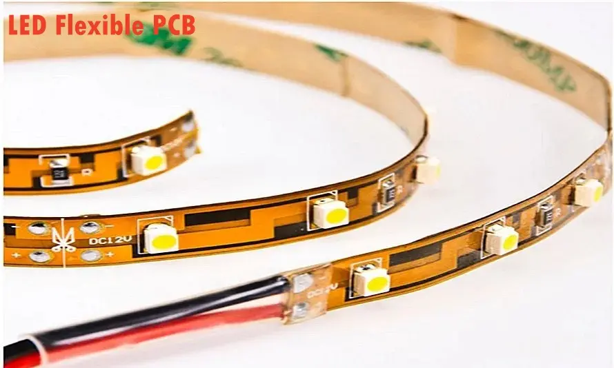
Flexible PCB
RAYMING is your one-stop PCB supplier for rigid-flex and flexible PCBs. We are a high quality quick turn prototype flexible and rigid-flex PCB manufacturer.
About Flexible PCB
Flexible PCBs (also known as flex circuits or flexible printed circuits) are made with a flexible dielectric polymer base (like polyimide or polyester) and copper traces. Unlike rigid PCBs, they can bend, twist, and fold, making them ideal for compact, portable devices. Key advantages include flexibility, lightweight design, durability (withstanding millions of flex cycles), space-saving integration, and customizability in shape.
These properties enable flexible PCBs to meet the physical and electrical demands of dynamic, compact electronics that rigid boards cannot.
Flexible PCB Products
Manufacturing Capability
Item | Description | |
Layer | Flexible board: 1-12Layers Flex-Rigid Board: 2-32Layers |
|
Material |
PI, PET, PEN, FR-4,dupont |
|
Stiffeners |
FR4, Aluminum, Polyimide, Stainless Steel |
|
Final Thickness | Flexible board: 0.002″ – 0.1″ (0.05-2.5mm) Flexible-rigid board: 0.0024″ – 0.16″ (0.06-4.0mm) |
|
Surface Treatment | Lead-free: ENG Gold; OSP, Immersion silver, Immersion Tin | |
Max / Min Board Size | Min: 0.2″x0.3″ Max: 20.5″x13″ | |
Min Trace Width / Min Clearance |
Inner: 0.5oz: 4/4mil Outer: 1/3oz-0.5oz: 4/4mil 1oz: 5/5mil 1oz: 5/5mil 2oz: 5/7mil 2oz: 5/7mil |
|
Min Hole Ring | Inner: 0.5oz: 4mil Outer: 1/3oz-0.5oz: 4mil 1oz: 5mil 1oz: 5mil 2oz: 7mil 2oz: 7mil |
|
Copper Thickness | 1/3oz – 2oz | |
Max / Min Insulation Thickness | 2mil/0.5mil (50um/12.7um) | |
Min Hole Size and Tolerance | Min hole: 8mil Tolerance: PTH±3mil, NPTH±2mil |
|
Min Slot | 24mil x 35mil (0.6×0.9mm) | |
Solder Mask Alignment Tolerance | ±3mil | |
Silkscreen Alignment Tolerance | ±6mil | |
Silkscreen Line Width | 5mil | |
Gold Plating | Nickel: 100u” – 200u” | Gold: 1u”-4u” |
Immersion Nickel / Gold | Nickel: 100u” – 200u” | Gold: 1u”-5u” |
Immersion Silver | Silver: 6u” – 12u” | |
OSP | Film: 8u” – 20u” | |
Test Voltage | Testing Fixture: 50-300V | |
Profile Tolerance of Punch | Accurate mould: ±2mil | |
Ordinary mould: ±4mil | ||
Knife mould: ±8mil | ||
Hand-Cut: ±15mil |
Flexible PCB Manufacturing Process
Material Preparation (Pre-Clean)
Production panels chemically cleaned, prior to application of circuit forming photo resist film, to ensure proper film adhesion. Conveyorised process utilizing thin core handling equipped systems to prevent damage to ultra thin material cores.
Flexible Circuit Pattern Exposure
Photo resist coated panels, overlayed with circuit artwork patterns, exposed with collimated UV light to transfer circuit image(s) to production panels. Both sides exposed simultaneously if required.
Etch Process
Circuit patterns chemically etched using specialized thin core handling equipped conveyorized systems. Both sides of panels etched simultaneously if required.
Drilling Process
High speed, high precision, small hole capable, drilling systems create required circuit hole patterns in production panels. Laser based systems available for ultra small hole requirements.
Copper Plating Process
Fully automated electrolytic copper plating systems deposit required additional copper within plated through holes to form layer to layer electrical interconnects.
Flexible Coverlay Application
Polyimide Coverlays aligned and tacked into place on production panels prior to Coverlay lamination process.
Flexible PCB Lamination
Flexible Coverlays laminated to production panels under heat, pressure and vacuum to ensure proper adhesion.
Stiffener Application
Localized additional stiffeners (if required by specific design) aligned and applied prior to additional lamination process under heat, pressure and vacuum.
Electrical Test
100% netlist driven electrical test per IPC –ET-652. Simultaneous testing of all circuits for continuity and isolation. Both grid and flying probe test systems utilized.
Final Fabrication
Individual parts die cut from production panel using high precision male / female punch and die sets. Other methods include laser cutting, mechanical routing, steel rule dies and chemically milled dies depending upon specific design requirements.
Flexible Design Guidelines
The bend radius is the minimum degree up to which the flex area can bend without damage. It must be properly identified early in the design. This ensures that your design allows the necessary number of bends without damaging the copper.
There are two types of FPCs:
- Static: These boards will flex less than 100 times in their lifetime. They will only flex during the installation process.
- Dynamic: FPCs flex during their operation. They are typically used in printers.
10 tips to design reliable bend areas:
- Clearly define the rigid and flex regions and the bend radius early in the design stage.
- For dynamic applications, the bend radius should be 100 times the finished board thickness.
- If there are no traces in the bend region, insert circular cutouts with radii greater than 30 mil to minimize the amount of material that needs to be deformed and increase flexibility.
- Avoid plated through holes and component placement within the bend area. Place plated through holes (PTH) at least 20 mil away from the bend area.
- Avoid 90˚ bends as they increase the risk of circuit damage. Instead, have gradual bends that are considered safer for the circuit.
- Place conductors smaller than 10 mil inside the neutral bend axis, where tension or compression is minimal during flexing.
- Provide sufficient space between the transition point of flex and the rigid area from the bending point to minimize the stress on the flex layers.
- Use tear guards to reinforce the flex material along the inside bend radius. This will prevent the flex material from tearing.
- Maintain at least 10 mil clearance between two flex regions. With inadequate clearance, adjacent flex regions may mechanically interfere with each other, leading to bending restrictions, increased stress on the material, or even tearing.
- Use cross-hatch for ground and power planes to reduce copper on a plane layer and increase the board’s flexibility. Typically, we recommend 0.015” wide signals with 0.025” spacing for the cross-hatched plane layers.
There are two types of flex materials:
- Adhesive-based material: The copper is bonded to the polyimide with acrylic adhesive.
- Adhesive-less material: The copper is cast directly onto the
The use of adhesives in rigid areas can create cracks in via plating. This is because acrylic adhesives become soft when heated. Consequently, when designing for adhesive-based materials, it’s important to incorporate anchors and teardrops in your design.
4 material selection guidelines for your flex printed circuits:
- Prefer adhesive-less materials for high-speed applications due to their consistent results and cost-effectiveness. If you are choosing adhesive-based material, have acrylic adhesives of 1 mil thickness.
- If you’re mounting components on flex sections, nclude PCB stiffeners for mechanical support. Use Kapton when the stiffener thickness is less than 10 mil.
- Use rolled annealed copper as cladding for polyimide flex cores.
- Select polyimide as the primary material for coverlay. It offers uniform thickness (min. 1 mil).
6 routing strategies you should know before designing a flex circuit board:
- Stagger traces when designing multi-layer flexible PCBs,. Stacked traces will not only reduce the flexibility of your circuit but will also increase stress, contributing to the thinning of copper circuits at the bend radius.
- Keep the traces perpendicular to the bend area to eliminate the stress points that can cause trace copper breakage.
- Avoid sharp corners in the flexible areas as they can lead to stress concentration and potential failure. Use rounded corners instead.
- Taper down the pads towards the end at which they are connected to the traces. This eliminates the issue where the trace entering a pad forms a weak spot, potentially causing copper fatigue over time.
- Do not include via-in-pad in flex designs, as it can damage the thin substrate during planarization. Moreover, the smaller aspect ratio of the vias does not allow non-conductive epoxy filling, and it can hamper the electrical conductivity of the vias.
- Implement additional through-hole plating of up to 1.5 mil to provide mechanical support from one flex layer to another.
9 ways to design reliable vias on flex boards:
- Teardrop annular ring when dealing with traces thinner than 20 mil to enhance the board’s structural integrity against shear force and vibrations.
- Incorporate anchors and spurs encapsulated with coverlay to avoid trace lifting and pad peeling.
- Avoid vias in the flex section of dynamic boards, as they are at risk of cracking
- Maintain at least 50 mil space between the vias and the stiffener’s edge. Vias are safe over a stiffener, but those placed just off its edge risk cracking.
- Place vias at least 30 mil away from the rigid-flex/flex interface.
- Maintain a hole-to-flex distance of 50 mil to increase the board’s reliability. This distance can be reduced to 30 mil for commercial applications. Insufficient clearance can generate undesired stress during bending and detach the via from its plating.
- Prefer pad-only plating (button plating) for flex boards. In this process, copper is deposited only on the vias/pads, reducing the amount of copper, which increases the board’s flexibility. Further, it aids in improving etch yields in small etch patterns by allowing manufacturers to control the copper thickness. However, the extra processing steps make this expensive.
- Keep the drill-to-copper distance of around 8 mil to achieve accuracy in layer alignment. This aids in the manufacturing process as flex materials are prone to more movement and contraction.
- Keep the annular rings as large as possible (at least >8 mil) to improve the mechanical strength of the connection.
The stiffener is an additional mechanical piece that provides mechanical support to your PCBA. By adding localized rigid material, single-sided, double-sided, and multilayered flex boards can be stiffened in specific areas.
Request a stack-up from your manufacturer in the design phase. It is crucial that you know what stack-up you are designing. Rigid-flex is the simplest configuration that will allow you to reduce the number of connectors, which will also increase wiring density and reliability.
Having a face-to-face meeting with the supplier is the best way to ensure that you’re on the same page in terms of where the overall PCB process is headed. This meeting can also help ensure that flex PCB layout techniques and capabilities are well understood.
6 design tips to build flex and rigid-flex stack-up:
- Position the flex layers in the stack-up’s center to provide protection from exposure to outer-layer plating. This placement also simplifies manufacturing and improves impedance and control in the flex area.
- Use an even number of layers to ensure a balanced stack-up.
- Utilize CAD tools for virtual mock-ups during the early design phase. You can create flex board models using stiff paper or mylar.
- Provide impedance trace details such as trace width, height, and impedance tolerance in the stack-up.
- Use bookbinding in rigid-flex boards, allowing more flex layers to navigate tight bends without deformation. It allows the PCB to perform bends of 180˚ or more. However, a board with bookbinding costs 30% more than a standard rigid-flex one.
- Implement the rigid-flex air-gap construction method to eliminate the flex adhesives within the rigid sections. This method also addresses the via reliability issues and improves bendability.
Material, Design, Types and Functions
- What is a Flexible PCB?
- Flexible PCB Materials and Construction
-
Flexible PCB Design Considerations
- Common Flex PCB Types and Applications
- Benefits and Advantages of Flex PCBs
- Future Trends in Flexible PCBs
- Conclusion and Summary
A flexible PCB uses a dielectric base layer made of a flexible polymer material such as polyimide or polyester. The conductive copper traces are laminated onto the flexible base layer to create a thin, bendable circuit board. The lack of rigid fiberglass reinforcement allows the flex PCB to be dynamically flexed and contorted during use.
Common names used to refer to flexible PCBs:
- Flex circuits
- Flexible circuits
- Flexible printed circuits
- Flex prints
Some key properties that differentiate flex PCBs include:
- Flexible – Can bend, twist, fold to conform around structures
- Lightweight – Extremely thin flexible material
- Dynamic – Repeatedly flexing, rolling, folding in use
- Durable – Withstands millions of flex cycles
- Integrated – Interconnects can be components themselves
- Space saving – Tightly integrates with products
- Customizable – Can be fabricated in any 2D shape
These capabilities allow flexible circuits to meet the complex physical and electrical demands in compact, portable electronic devices that rigid boards cannot satisfy.
The unique materials and construction of flexible PCBs enable their distinct capabilities. The key components of a flex circuit’s build are:
Dielectric Flexible Substrate
The base dielectric layer provides the foundation upon which the conductive traces are fabricated. Choosing the right flexible substrate material is critical. Common options include:
- Polyimide (Kapton) – Most popular, high temp rating, excellent chemical resistance
- Polyester (PET) – Lower cost, moderately high temp rating
- Polyamide – Flexible even at low temps
- Fluoropolymers (PTFE) – Superior chemical resistance, relatively expensive
- Liquid Crystal Polymer (LCP) – High frequency, low signal loss
Polyimide is the most widely used flex substrate material given its high durability, thermal properties and cost-benefit ratio.
- Copper Foil
- Conductors
- Coverlay
- Bonding Adhesive
- Stiffeners
- Finish and Coatings
Designing a reliable flex PCB requires special considerations for the dynamic bending aspects. Here are some of the key guidelines.
- Trace Width and Spacing
- Bend Radius
- Coverlay Voids
- Reinforcement
- Adhesives
- Vias
- Corners
- Pads
- Shielding
By adopting and evolving such specialized guidelines, flex PCBs can be designed to survive millions of flexing cycles with long product lifetimes.
Flexible circuits can be implemented in several configurations for interconnect and packaging applications:
- Flexible Interconnects
- Flexible Cables
- Membrane Switches
- Flex Rigid Boards
- Flexible Heaters
Some common flex PCB applications are:
- Medical instruments
- Wearable devices
- Robotics and industrial machines
- Consumer electronics
- Automotive electronics
- Aerospace and military systems
The compact, lightweight and dynamic characteristics of flex circuits open up innovative design possibilities.
Here are some of the key benefits provided by flexible PCB technology:
- Dynamic Flexing – Withstand millions of movement cycles enabling rolling, twisting, folding which is impossible with rigid PCBs.
- Conforms to Shape – Can tightly integrate with product contours and housings unlike rigid boards.
- Lightweight – Extremely low mass compared to rigid laminates allows portable, wearable devices.
- Thin Form Factor – Compact, low-profile circuits to fit small spaces and enable thinner products.
- Durable – Flexible construction is resistant to vibrations and mechanical shocks.
- High Density – Integrates interconnects avoiding external cables and connectors.
- Custom Shapes – Can be produced in unlimited 2D shapes and outlines.
- Soft and pliable – Allows integration of complete electronic systems into fabrics.
- Reliability – Offers consistent performance over flex life with proper design.
- Cost Savings – Removes connectors, simplifies assembly and lowers total product cost.
Here are some key trends shaping the continued evolution of flexible PCB technology:
- Thinner Constructions – Reducing flexible layer thicknesses down to 1 mil to improve bendability.
- Smaller Features – Narrower trace widths and spacing down to 2 mils to increase integration.
- Improved Materials – New substrates like LCP for better electrical and high frequency performance.
- Fine Pitch Components – Enabling direct surface mount of ultra-fine pitch ICs on flex PCBs.
- High Density Flex – Development of flexible multilayer boards up to 12 conductive layers.
- Embedding Passives – Incorporating thin embedded resistors and capacitors within the flexible layers.
- Stretchable Circuits – Adopting novel materials to allow flexible PCBs to stretch and deform.
- Additive Processing – Transitioning from subtractive etching to additive fabrication using printing or plating processes.
- 3D Structured Flex Circuits – Techniques to fabricate out-of-plane flex circuit structures.
As material science and manufacturing processes mature, flex PCB technology will open doors to more innovative electronics designs not feasible before.
Key takeaways:
- Flex PCB technology enables flexible, lightweight and dynamic circuits through specialized materials and construction.
- Polyimide is the most popular flexible dielectric substrate paired with ultrathin copper foils.
- Flexible PCB properties support tight bend radii down to 3-10X the total thickness.
- Careful design considerations are critical for dynamic flex performance and reliability.
- Flex circuits are widely used for compact and portable electronics designs requiring flexibility.
- Flex PCBs provide unique advantages but have limitations in layers, density and power handling.
- The technology continues to evolve with thinner, higher density and more capable implementations.
With their distinct capabilities and advantages, flexible PCBs will continue growing as an interconnection method supporting electronics miniaturization across industries.