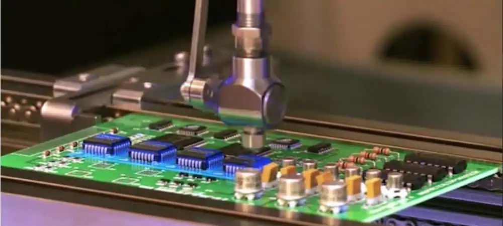
What is PCB Edge Plating?

pcb edge plating

Introduction

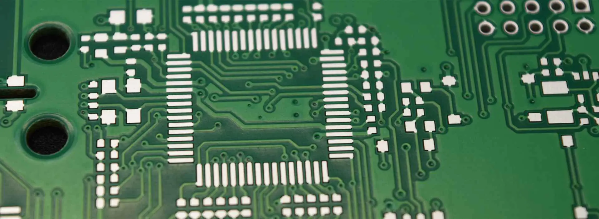
PCB edge plating is the process of plating exposed copper connections along the edges of a printed circuit board with a metallic coating like gold or tin to facilitate electrical connections. This article provides a comprehensive overview of PCB edge plating including its purpose, edge connector types, plating processes, inspection, reliability factors, and future trends.

What is a PCB Edge Connector?

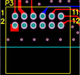
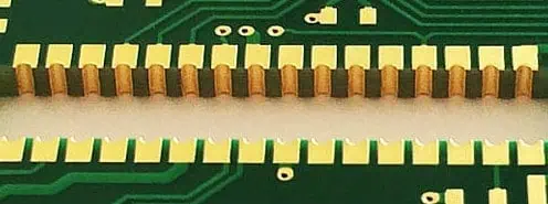
A PCB edge connector refers to the gold plated contact fingers or pads arrayed along one or more edges of a circuit board that mate with a corresponding connector. The board edge fits into a slot to make electrical contact.

Edge connectors allow boards to be easily installed, removed, and replaced from electronic systems.

Why Use PCB Edge Connectors?

Key benefits of edge connectors:

  • Allow insertion/removal of PCBs from system
  • Wipe contact action for reliable connections
  • Component-less connections simplify assembly
  • Easy to fabricate and integrate on PCB
  • No soldering required
  • Withstand thousands of mating cycles
  • Support high density contact configurations
  • Enable high frequency signaling

These factors make edge connectors highly versatile and cost-effective.

Types of Edge Connectors

Copper-to-pcb-edge

Common edge connector configurations include:

Single Row Edges

  • One row of contacts on board edge
  • Less costly, lower density
  • Used for prototypes or low complexity

Dual Row Edges

  • Two parallel rows of staggered contacts
  • Allows higher number of connections
  • Improves mechanical alignment

Multi-Row Edges

  • More than two rows, or rows on multiple edges
  • Further increases connection density
  • Complex PCB layout

High Density Edges

  • Very narrow pitch between contacts
  • Up to 600+ connections on single edge
  • May use dual-beam cantilever contacts

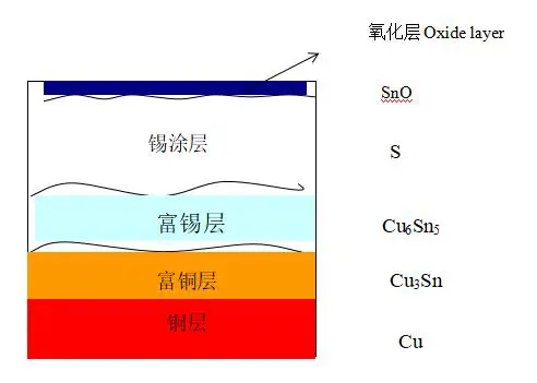
Edge Contact Plating

To provide conductivity and protect copper traces, edge contacts require metallic plating like:

  • Gold – Most common, resistant to oxidation/corrosion
  • Tin – Lower cost but susceptible to oxidation over time
  • Palladium-Nickel – Avoid tin whisker issues, lower cost
  • Gold Flash over Nickel – Combines low cost nickel with gold outer layer

A minimum thickness like 50 ฮผin of gold ensures durability over 10,000+ mating cycles.

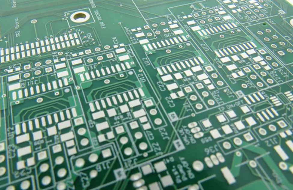
PCB Edge Plating Process Steps

A typical PCB edge plating process involves:

  1. Drilling holes for edge contacts
  2. Copper electroless then electrolytic plating
  3. Etching to form isolated traces
  4. Surface preparation like microetching
  5. Immersion plating of gold or other metal
  6. Cleaning then drying boards
  7. Quality inspection – thickness, continuity, defects
  8. Electrical testing if needed

Fabrication generally follows standard PCB methods plus final plating.

Edge Plating Quality Control

Key process controls needed:

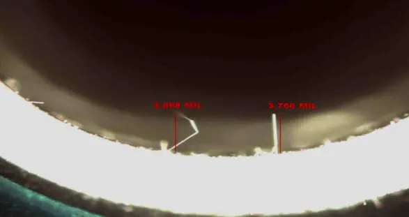
  • Plating Thickness – Confirm minimum thickness met via microscopy or X-ray fluorescence. Insufficient plating risks wear or corrosion issues.
  • Continuity – Verify electrical connectivity from inner layers through plated edge contacts.
  • Plating Coverage – Inspect for voids or thin areas around traces.
  • Overplating – Ensure plating does not excessively build up on glass weave. Can impede mating.
  • Trace Geometry – Confirm dimensions match specifications.

Reliability Considerations

Several factors impact connector lifespan:

  • Plating thickness – Thicker gold or tin plating improves cycle life and durability.
  • PCB thickness – Boards thinner than 1 mm may bow during mating stress.
  • Contact geometry – Well-designed trace shapes tolerate repeated mating forces.
  • Receptacle contacts – Select robust and proven connector contact designs to match.
  • Contamination – Prevent dirt, oils, or particles during handling and use.

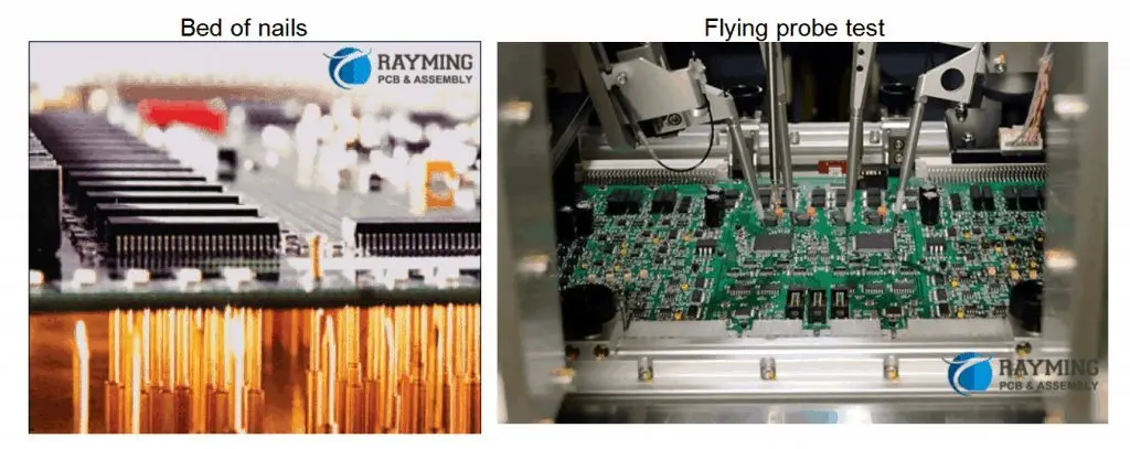
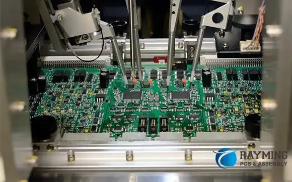
Inspecting Assembled Connections

Key checks on completed connectors:

  • Continuity – Spot check electrical conductivity through mated connection.
  • Contact Engagement – Confirm full insertion with visual checks.
  • Marks/Damage – Inspect for signs of wear, scrapes, or damage after assembly cycles.
  • Contamination – Verify absence of particles or films from handling.

Edge Connector Standards

Key specifications and standards for edge connectors:

  • IPC-2223 – Sectional requirements for PCB edge contacts
  • IPC-6013 – Qualification and performance of edge connections
  • IPC/EIA J-STD-002 – Solderability tests for component leads/terminations
  • IEC 60352-5 – Reliability testing and requirements

Compliance to standards ensures quality and reliability goals are met.

PCB Layout Guidelines

To optimize edge connector performance:

  • Minimize total board thickness
  • Ensure adequate board rigidity
  • Include integrated stiffener ribs if needed
  • Avoid placing components along connector edge
  • Include generous fillets at trace corners
  • Fanout inner layer traces gradually

Reviewing layouts with the receptacle supplier is recommended.

Edge Connector Applications

Edge connectors see wide usage across:

  • Computers – Daughtercards, memory modules, backplanes
  • Telecom – Switching cards, router cards, base stations
  • Military/Aerospace – Mission systems, navigation cards
  • Medical – MRI, ultrasound, imaging cards
  • Automotive – Engine control units, instrument clusters
  • Consumer – Set-top boxes, game consoles

Edge connectors enable quick field replacement of electronics cards or modules across industries.

Future Trends

Edge connector technology continues advancing:

  • Increasing Density – More contacts in thinner boards enabling complex interconnection.
  • Higher Frequencies – Extending signal integrity to 10+ Gbps rates.
  • Improved Durability – Advanced plating and contact shaping for 10,000+ mating cycles.
  • Lower Costs – Simplified fabrication allowing broader adoption.

Connector manufacturers and PCB fabricators are driving progress.

Conclusion

In summary, PCB edge plating and connectors offer a versatile and cost-effective interconnection method widely used for replaceable subsystems, cards, and modules across many industries. Edge connectors will continue meeting the challenges of denser contacts, thinner boards, faster signaling, and improved reliability thanks to ongoing advancements in plating technology, board materials, and precision manufacturing techniques. While alternative approaches like board-to-board connectors exist, the simplicity and convenience of edge connectors ensures their usage well into the future anytime field replaceability of circuits is required.

FAQs

Q: What is the most common metal used for edge connector plating?

A: Gold is by far the most popular thanks to its durability and resistance to corrosion and oxidation over thousands of mating cycles.

Q: What are some key reliability concerns with edge connectors?

A: Insufficient plating thickness, contamination, poor contact design, and inadequate board thickness or rigidity impact connector lifespan.

Q: How many mating cycles can a robust edge connector withstand?

A: Well designed gold plated connectors using suitable PCB thickness can achieve 10,000 cycles or more.

Q: What are some alternatives to PCB edge connectors?

A: Board-to-board connectors, hybrid edge connectors, and high density board stacking connectors offer other options.

Q: What is the main benefit of using dual row edge connectors versus single row?

A: Dual row configurations double the connection density by interleaving two staggered rows of contacts.

How to do PCB edge plating ?

PCB edge plating

At present, there are two kinds of PCB board edge design: metallization and non-metallization. For non-metallization, manufacturers in the industry have matured, but the metallization technology is still immature. Nowadays, more customers’ production needs are turning to PCB metal edging. Therefore, the quality of PCB metal edging has become the focus of customers’ and manufacturers’ attention because its quality directly affects the use of products.

The necessity of PCB metal edging

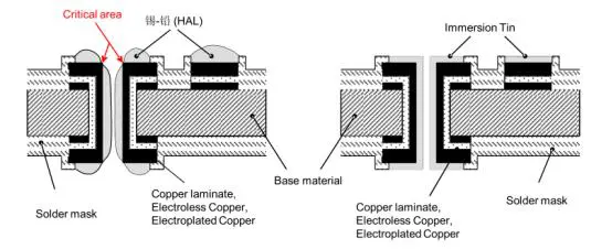
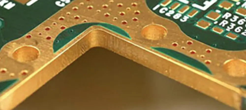
Metalized edging means that the edge of the board must be metalized. English description: Edge plating, border plated, plated contour, side plating, side metal, etc.

More electronic products start to minimize the product volume as the goal so that PCB will use electroplated nickel and gold surface treatment(ENIG) technology. In the production process, the gold-plated finger process can achieve the gold-cladding of the solder joints. Still, it is necessary to separately make the lead-through solder joints and the board edges, even though they are removed after gold plating. It is only convenient for the production of gold-clad solder joints on the side of the board. The production process of electroplating nickel gold is simple. It is unnecessary to make the leads separately, but only the top layer of the solder joints can be plated with gold, and the side plated with gold can not be produced. The gold-plated nickel-gold plating process on the side of the circuit board can achieve the top layer gold plating and the side-side gold plating at the same time.

Metallization edging process:

Drilling —- Milling metalized slot hole —- Removing dirt —- Plated-through hole

Altium edge plating

Drawing of engineering documents for metallized edging

  1. Determine the area where the board needs to be metalized.
  • When most customers are designing the circuit, the copper is stretched out on the outer edge of the board. When this happens, you need to consider whether the edge of the board needs to be hemmed and if the metalized edging is needed during production (must require formal instructions from the customer).
  • Sources of information: One is Gerber files, and the others are PDF, TXT, DWG, etc.
  • Design and precautions of metallized edging board
  • Copy the outline layer in the design file to the pthrou layer to make a closed long slot.
Edge plating

Note that since copper plating is required at the encapsulation, the copper thickness has a specific thickness. Therefore, when making the hemming shape, compensation should be considered.

  • After finishing the edging groove, the next step is to determine the electrical connectivity of the edging.

In order to determine which layer should be connected to the hemming, the following sequence should be followed:

  • Find out which layers and areas the customer requires to connect.
  • Clear the connection requirements of each layer.
  • Precautions for the production of metalized edging lines
  • For the edged board, in order to prevent film chipping, it is necessary to ensure that the pad is 10MIL on one side. Whether in the board, on the side, or outside the board, it must have a 10MIL pad. If it needs to be added or changed, it must be confirmed by the customer. If there are pads near the edging, the pads’ distance and the edging disk should be at least 8MIL. If it cannot be satisfied, feedback and confirmation are required.
  • After the hemming, the connection of the inner and outer layers must be checked. The connection method between the layers must be determined to avoid electrical and ground short circuits after the hemming.
  • If there is a plated film, the edging must be processed like a PTH groove, and there must be a disk. Pay special attention: the edging of the special-shaped groove should also be the same as the hole, which needs to be filled and enlarged by 4mil.

Solder mask design for metallized edging

For the solder mask, the edging groove must be fully windowed.

  • Bounding solder mask opening = Bounding pad +0.16mm

Outline problem for metallized edging

PCB side plating

In order to improve production efficiency, CAM must use standard milling cutters to make edging grooves, such as: 0.8, 1.0, 1.6, 2.0, 2.4mm.

Remarks: If this is not in the customer’s requirement, please choose 2.0mm or greater.

Panel design requirements and choice of surface treatment

  • The long direction of the edging slot must be parallel to the long side of the rear panel (the direction of the edging slot is parallel to the running direction of the tin spray).
  • For orders that do not meet the above requirements, the project pre-review will require the customer to confirm the use of non-sprayed surface processes such as gold or copper-nickel plating.

Other matters needing attention

  • If the antenna position is too large, it will affect the customer’s welding or signal transmission.
  • The inner cladding pad is connected to the wire in the board, causing a Short circuit.
  • The stamp hole is designed at the edging slot, which must be treated with two drills.

Remarks:

If the stamp hole is placed in a drill, the plate may break due to the irregular forces when the plate swings back and forth in the electroplating cylinder.

If the bridge width is insufficient when spraying tin, the plate may break due to the force of the wind knife when spraying tin.

The production process of plate-side gold-plated nickel-gold plating:

PCB side plating

The process of plating the sidewalls of the circuit board with gold and electroplating nickel and gold includes:

  1. Etching – Forms an etching groove on the copper surface of the circuit board. The etching groove extends along the pattern to be coated with gold on the sidewall, so that the copper layer needs to be coated with gold.
  2. The side walls are exposed – A dry film is pasted on the copper layer, and an opening is formed on the dry film. The opening corresponds to the etching groove and the area of the copper plate surrounded by gold that needs to be covered with gold.
  3. Expose the side walls – Electroplating the circuit board so that the copper plate area and the side walls are plated with a layer of nickel and gold.

If the copper plate area is an independent pad, lead is separately added.

The distance between the circumferential edge of the window and the circumferential edge of the copper plate area is 4 mils.

During electroplating, nickel and gold are formed on the upper surface and sidewalls of the copper plate area at the same time to achieve the top layer gold plating and the sidewall gold coating.

edge plating

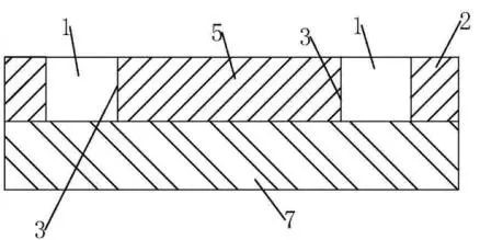
Description of the drawings

Reference signs in the figure: 1. Etching groove, 2. Copper layer, 3. Sidewall, 4. Dry film, 5. Copper plate area, 6. Open window, 7. Substrate, 8. Open window, 9. Dry film.

Specific operation instructions:

The gold plating nickel-gold electroplating process on the sidewall of the circuit board includes: Forming an etching groove (1) on the copper surface of the circuit board by etching. The etching groove (1) extends along the pattern to be coated with gold on the side of the board; this is why the copper layer (2) is required. The gold-clad sidewall (3) is exposed, and a dry film (4) is pasted on the copper layer (2). An opening (6) is formed on the dry film (4), which corresponds to the etching groove (1) and its surroundings. The copper plate area (5) that needs to be coated with gold is provided and exposed to the side walls. The circuit board is electroplated with nickel and gold so that both the copper plate area (5) and the side walls (3) are plated with a layer of nickel and gold.

When making a circuit board, as shown in Figure 1, paste a dry film (9) on the outer sidewall of the copper layer (2). Form an opening (8) on the dry film (9), which corresponds to the to-be-formed etching groove (1) and shape. Then, etching is performed, thereby forming an etching groove (1). One side wall (3) of the etching groove (1) needs to be side-clad with gold in the subsequent process.

Then, a dry film (4) is pasted on the outer wall of the copper layer (2). Simultaneously, the dry film (4) is formed with a window corresponding to the copper plate area (5) to be gold-plated, gold-clad on the side of the board, and the etching groove (1) around it.

Finally, it’s time to electroplate the circuit board. Since the upper surface and side surfaces of the copper plate area (5) are not covered with the dry film (4), nickel and gold can be formed on the upper surface and sidewalls of the copper plate area (5) during electroplating. This is to achieve top-layer gold plating and board edge gold plating at the same time.

Preferably, if the copper plate area (5) is an independent pad, a lead is added separately.

Preferably, the distance between the circumferential edge of the window (6) and the circumferential edge of the copper plate area (5) is 4 mils. In this way, it is convenient for the syrup to enter the pad’s sidewall position, and gold-cladding on the side of the board is achieved when electroplating is complete.

Technical characteristics of the gold plating on the sidewall of the circuit board:

A process for coating the sidewalls of a circuit board with gold and electroplating nickel and gold is characterized in that it comprises:

  • An etching groove is formed on the copper surface of the circuit board by etching. The etching groove extends along the pattern to be coated with gold on the sidewall. This exposes the sidewall of the copper layer that needs to be coated with gold.
  • Paste a dry film on the copper layer, and form a window on the dry film. The window corresponds to the etching groove and the area of the copper plate that needs to be covered with gold and exposed to the sidewall.
  • Electroplating the circuit board with nickel and gold so that the copper plate area and the sidewall are plated with a layer of nickel and gold.
  • The process of plating the sidewall of the circuit board with gold and electroplating nickel and gold is that the distance between the circumferential edge of the window opening and the circumferential edge of the copper plate area is 4 mils.

With the increase of system speed, the timing and signal integrity problems of high-speed digital signals are important, but the EMC problems caused by the electromagnetic interference and power integrity in the system are also critical. The electromagnetic interference generated by the high-speed digital signal will cause serious mutual interference within the system and reduce the system’s anti-interference ability and generate strong electromagnetic radiation to the outer space.

This causes the system’s electromagnetic radiation emission to seriously exceed the EMC standard, making the product unable to pass EMC standard certification. The side-board radiation of a multilayer PCB is a relatively common source of electromagnetic radiation. When the unexpected current reaches the edge of the ground plane and the power plane, edge radiation occurs. The PCB board metalization edging process encloses the entire board edge with metal, so that the microwave signal cannot be radiated from the PCB board edge, thereby solving the problem of edge radiation. Of course, the use of the board edge metallization edging process will also increase the manufacturing cost of the PCB.

RayMing Electronics Co., Ltd. is a professional manufacturer of high-precision multilayer circuit boards, module immersion gold circuit boards, automotive circuit boards, driving recorders, COB power supplies, computer motherboards, medical circuit boards, module bonding boards, blind hole impedance board, thermoelectric separation copper substrate, etc. RayMing provides top-notch quality assurance and punctual delivery, a high-tech enterprise with sales as a whole. If there is a demand for side-coated gold boards, please feel free to contact us!

What is Wire Bonding?

wire bonding

WirebondingTemperature (oC)PressureWireUltrasonic energy
Thermocompression300 โ€“ 500HighAuNo
Ultrasonic25LowAu, AlYes
Thermosonic100 โ€“ 150LowAuYes

Introduction

Wire bonding is a method used to electrically and mechanically join conductive wires to semiconductor chips and substrates to make interconnections. It is a key process used extensively in the assembly and packaging of integrated circuits (ICs). This article provides a comprehensive overview of wire bonding fundamentals, bonding techniques, materials, processes, inspections, applications, advantages and challenges.

Definition of Wire Bonding

Wire bonding attaches thin wires to electrically connect the contact pads on ICs to the leads or bonding areas on printed circuit boards or other assemblies. It forms a bridge to allow electrical signals to cross gaps between the IC and substrate.

The wire bonds also help conduct heat and provide shock protection to the chip.

Why Use Wire Bonding?

PCB Wire Bonding
  • Provides electrical connectivity for IC chips
  • Allows routing signals in 3D space
  • Bridges gaps between ICs and substrates
  • Bonded wires are flexible
  • Very precise bonding placement
  • Can support high frequencies and data rates
  • Cost effective for mass production

Wire bonding is a mature and reliable interconnect technology suitable for most IC assembly applications.

Types of Wire Bonds

The main types of wire bonds used are:

Ball Bonds

A ball bond is formed by melting the end of the wire into a sphere using a flame, spark discharge or electric arc and pressing it against a bond pad under force and ultrasonic energy. This creates the initial connection.

Wedge Bonds

A wedge bond is made by pressing a wire against the bonding area through a wedge-shaped bonding capillary, deforming it and pressing it against the surface under force and ultrasonic energy. The wire is then torn at the edge of the capillary tip.

Ribbon Bonds

Ribbon bonding joins a thin flat wire to the IC die or substrate in the same manner as round wedge bonding. It makes multiple bonds simultaneously in parallel.

Wire Bonding Techniques

IC Bonding

The main wire bonding techniques include:

Thermosonic Bonding

Using a combination of heat and ultrasonic energy, along with force, to weld the wire to the bonding area. It is used for both ball and wedge bonding.

Thermocompression Bonding

Applying heat, force and welding pressure through the bond tool tip to deform the wire and bond it to the area. Mainly used for ball bonding.

Ultrasonic Bonding

Utilizing just ultrasonic energy and force to create a cold weld between the wire and bond area. Used for aluminum wire wedge bonding.

Wire Bonding Materials

Common wire materials include:

  • Gold – Most prevalent, offers very reliable bonds
  • Copper – Lower cost than gold, challenges with oxidation
  • Aluminum – Only for ultrasonic wedge bonding
  • Silver – Good electrical properties but bonds less reliably

Gold wire is generally preferred for critical electronics due to its excellent conductivity, bondability and corrosion resistance.

Wire Properties

Key wire properties for bonding include:

  • Composition – Gold, copper, aluminum etc.
  • Diameter – Typically 15 to 50 ฮผm
  • Temper – Annealed soft vs hard temper
  • Coatings – Bare or coated with alloys
  • Shapes – Round, ribbon, shaped customized wires

The composition, diameter and temper determine the best bonding approach.

Bonding Process Steps

Basic wire bonding process flow:

  1. Prepare bond sites – Clean pads, apply heat
  2. Position wire – Thread through capillary tip
  3. Form first bond – Ball or wedge bond on chip die
  4. Extend wire – Feed out to leadframe/substrate
  5. Form second bond – Wedge bond wire to destination
  6. Repeat bonding – For multiple wire connections
  7. Cut excess wire – Sever final bond

This sequence is computer numerically controlled for automation.

Wire Bonding Equipment

  • Bonding Tool – Precisely positions capillary tip
  • Work Holder – Secures substrate using heating/cooling
  • Ultrasonics – Provides ultrasonic vibration energy
  • Vision – Aligns tools and materials optically
  • Wire Feed – Feeds wire on demand during bonding
  • Controls – Automates all parameters and positioning

Sophisticated wire bonders provide the accuracy, speed and flexibility needed.

Advantages of Wire Bonding

  • Mature and well established technology
  • High throughput and automation
  • Handles high density I/O pitch <40 ฮผm
  • Low parasitic capacitance and inductance
  • High purity wires available
  • Adaptable to complex geometries
  • Allows stacking dies and interposers
  • Fine pitch capability down to 15 ฮผm
  • Cost effective for mass production

These benefits make wire bonding a widely utilized interconnect solution.

Wire Bonding Challenges

  • Limited by length-to-diameter aspect ratio
  • Wires block die access and view
  • Long wires may sag during encapsulation
  • Parasitic capacitance/inductance increase with length
  • Not well suited for high current due to wire gauge
  • Subject to corrosion and contamination over time
  • Bonds may fail due to temperature cycling or moisture
  • Repairs often require removing and replacing bonds

While very capable, wire bonds have inherent limitations.

Wire Bonding Inspections

Key wire bond quality inspections include:

Bond Placement Accuracy

Confirming correct positioning of each bond on its pad.

Bond Orientation

Checking orientation angle of wedge bonds against leadframe edges.

Bond Quality

Inspecting bond integrity – shape, attachment, lifted balls or wedges.

Wire Shape

Verifying proper loop height, placement and absence of kinks.

Wire Sweep

Checking wires are not excessively low from die to substrate.

Automated optical inspection improves quality and throughput.

Wire Pull Testing

bond strength can be measured by pull testing:

  • Uses hook or wedge tool to lift bonded wire
  • Gradually increases force until bond breaks or wire severs
  • Measures maximum force at failure in grams
  • Compare to minimum pull spec for acceptable strength

Manual or automated systems perform statistical sampling.

Process Controls

Key parameters requiring controls:

  • Bond force – Amount of force applied
  • Ultrasonic power – For thermasonic bonding
  • Bond time – Duration of bonding
  • Bond temperatures – Heating zones
  • Wire tension – Constant tension during feeding

SPC, visual checks, and product audits ensure stability.

Wire Bonding Applications

Wire bonding sees extensive usage across:

  • Consumer electronics – Mobile, IoT, wearables
  • Computing – Microprocessors, memory, chipsets
  • Automotive – Sensors, controls, infotainment
  • Aerospace/military – Guidance systems, radars
  • Medical – Implants, stimulators, imaging
  • Communications – 5G, networking hardware

Any application with ICs benefits from wire bonding technology.

Emerging Technologies

Some newer technologies aim to augment wire bonding:

Ribbon Bonding

  • Joins multiple wires simultaneously
  • Higher throughput bonding
  • Challenging ribbon handling

Stud Bumping

  • Deposit gold bumps on bond pads
  • Allows finer pitch than bond pads
  • Issue of bump bond reliability

Remote Plasma Bonding

  • Creates plasma for lower temperature bonding
  • Reduces damage to sensitive devices
  • Complex plasma generator required

These methods are still maturing toward volume adoption.

The Future of Wire Bonding

Despite competition from flip chip and other techniques, wire bonding will remain essential:

  • Ongoing materials and equipment innovations
  • Nano-scale wires enabling ultra-fine pitch
  • Extending capabilities to new applications
  • Allowing hybrid bonding with other interconnects
  • Roadmap to at least 10 years for next-gen adoption

Wire bonding equipment and material suppliers continue advancing this vital technology.

Conclusion

In summary, wire bonding provides a proven, adaptable, and cost-effective interconnect method widely adopted across the microelectronics industry. Advancements in bonding tools, materials, and process automation continue expanding capabilities while reducing cost even further. Despite some inherent limitations, wire bonding will remain an essential manufacturing process enabling ongoing miniaturization and performance increases of integrated circuits. Even as alternative approaches emerge, wire bonding delivers unique benefits for numerous applications demanding flexibile, fine pitch, and high throughput chip connections.

FAQs

Q: What are the main differences between ball bonding and wedge bonding?

A: Ball bonding forms an initial ball whereas wedge bonding uses the side of the wire pressed into the bond pad. Also, ball bonding can only make the first bond whereas wedge bonding can make both first and second bonds.

Q: What wire size is typically used for wire bonding?

A: Most wire bonding uses wire diameters in the range of 15 to 50 microns. Specialized nano-scale wire bonding can go below 15 microns.

Q: How close together can wire bonds be placed?

A: The finest pitch wire bonding today can achieve a density down to around 15 microns between adjacent connections.

Q: What is the key benefit of ribbon bonding versus round wire?

A: Ribbon bonding can make multiple wire bonds simultaneously, boosting throughput substantially compared to round wire.

Q: What is the main factor limiting the span between wire bonds?

A: The length to diameter ratio of the thin wire limits total wire length before unwanted sagging or sweeping may occur. Typical spans are under 5 mm.

Types of Bonding Based on Shape

Common bonding shape that is used nowadays are ball, wedge bonding and flip chip bonding. In recent times, people prefer using one shape to another. Then, Why the designer prefer to one method than another ? For comparing all methods, we will explain more and compare all bonding shapes in this articles.

Ball Bonding

Ball holding is the cycle where pads are bond into a silicon die and substrate or leadframe utilizing wire which has fine diameter. The essential process of ball bonding method involve the first bonding shaping (commonly above the chip), the second bond shaping (commonly on the substrate) and the wire loop.

On the start of the wire process, the bonding equipment move down until it reach first bond area. The first bond is accomplished by making bond between a pad and a spherical ball utilizing ultrasonic energy and heat treatment. The first bond is likewise alluded to ball bond. Looping movements are planned in program to meet the requirement of package for  loop shape and height.


The second bond includes stitch bond which bonds the tail bond and the opposite end. The tail bond is required to create a tail of wire for the following ball shaping process. After the bonding equipment moves up to release the wire tail, after that the tail is off and the bonding equipment ascends to the ball shaping height. The ball shaping process is accomplished by ionization air gap in a cycle called EFO or electronic fire off. The ball resulted on this process is called a FAB or free air ball.

Keeping ball size is important for this cycle as it sets the general size bond and is relying on dependable bonding process to guarantee a conformable length of wire tail before each ball shaping. In case each bond is not shaped appropriately, there will be huge bump sizing variations.

Mechanical force fine application is important in the bonding cycle as it also set bumpโ€™s height and form. At last, shearing step with precise determination to split up the the ball and wire is important to make planar and conformable height bond.

Wedge Bonding

The bottom side of the capillary is used to squeezed a wire stub toward the bond pad, using ultrasonic energy to shape the bond among bond pad and wire, In wedge bonding method. After that, the capillary move toward the second bond area and the cycle is processed with repeating those process. When the second bond is finished, the wire is clipped and snapped over the second bond.

The important process in the wire bonding cycle  comprise accomplishing dependable bond (including first, second, and tail bond), keeping up wanted loop, and placing the bonds precisely. Throughput is a necessary point too, as it influences the device production expense. Accomplishing wanted first bond and second bonds generally needs bonding parameters optimization. DOE or design of experiment should be used to exercise parameters optimization, that comprise effect ultrasonic energy levels, mechanical force, bonding power. An appropriate free air ball dimension regularly is resolved prior to starting the DOE first-bond. Looping directions are chosen by the application necessities. There are two common loop types and those are reverse and forward. Forward looping type firstly puts a ball bond over the die, and after that puts a stitch bond on lead frame. In the other hand, the first step in a reverse bonding type, nonetheless, is putting a bump die. Right after the bump is shaped, a ball bond is put over the substrate, then shaping the stich bond over the. Low-profile looping prerequisites have pushed the developing reverse ball bonding utilization, that is a less quick method than forward bonding method.

Application of Fine-pitch. fine-pitch wire bonding competence has been exhibited in lab at 35 ยตm pitch. Generally 15 ยตm wire is utilized with 35-ยตm pitch ball bonding and a bonded ball with diameter around 27 ยตm. Fine-pitch usage needs a higher wire bonder aptitude, such as better control of ultrasonic energy level, the bonding force, and also fine wires looping ability, that is more disposed to loop influence  and weaker. A wire bonder which fulfills the fine pitch needs ought to likewise having  precise movement and submicron accuracy on vision system.

Applications of Stacked Die. Stacked pass on implementations are one of the quickest developing patterns in the semiconductor business. The urge for lighter, more intelligent, and smaller gadgets encourage this 3-D packaging research and development. Stacked die usage present variance of wire bonding difficulties, including multi level and low loop wire bonding loop free space needed, loop resistance from wire clear during molding process , and bonding to hang unsupported die verge.

Most wire bonding implementation utilize the ordinary forward bonding method, since it is quicker and more adequate for finer pitch compare to reverse bonding method. Even though, forward ball bonding method has a restriction of loop height because of the neck region over the ball. Exaggerated bending over the ball can cause crack on the neck area, which brings about dependability issues. Reverse bonding can accomplish loop height smaller than 75 ยตm.

Flip-Chip Bonding

Flip chip bonding is a important innovation for cutting edge microelectronic circuits packaging. It permits connection of bare chip to a substrate for packaging in a face-down arrangement, with electrical associations among the substrate and chip through conductive bumps. Flip chip assembly has numerous benefits. A primer benefit is enhancing electrical performance. flip chip little bumps connection give short electrical ways, that yield incredible electrical properties which have low resistance ,capacitance, and inductance. This brings about extraordinarily improved performance in high frequency working when compared with other bonding techniques, for example, chip wire bond over substrate.

Another key benefit of flip chip assembly method is compactness of package which decrease weight and size contrasted with traditional wire bond method. The electrical interconnection between substrate surface and pads over chip can be spread out as a zone array, as opposed to around the chip that is a particular design for wire bond arrangement. This two dimensional structure can reduce chip footprint over substrate and reduce chip space. The small physical area and low profile of flip chip construction permit small electronic package size to be fabricated. Nowadays, you can find flip chip components in number hand held gadgets, PDAs, electronic coordinators, electronic watches, cameras, and any other products.

How to Choose Proper Bonding Shape for Certain Aim?

When we reach application step, we often deal with question which method that appropriate with our need: wedge bond, flip-chip bond , and ball bond? For which reason would an engineer pick a ball bonder and not a wedge bonder or the other way around? This question come to most the engineers, as a rule, electrical attributes of the package are influenced by the wire bonding technique. Even, there are situations where particular packages have physical restriction like temperature restriction (no heat or low heat usage), avoid gold material and choose aluminum, prefer using ribbon type to wire type and fine pitch usage. This is the case where the appropriate selection of wire bond method becomes play an important role.

Commonly, ball bonding implementation are related to thermosonic and thermocompression bonding techniques. Thermocompression uses temperature from around 150oC and mechanical pressure to make intermetallic bonding. And thermosonic adds energy from ultrasonic from the past step. With the two techniques, in any case, sparkle from an EFO or electronic fire off  under the capillary create a free air ball prior to bonding shaping. This free air ball at that point deform when the capillary directly contact with the bond pad surface and applies ultrasonics and mechanical force for several time to change ball shape. Hence the interdiffusion between the bond pad and the wire metallization happens, that creates the intermetallic bond.

Until this day, over  90% of all wire bonds method in electrical packaging use gold ball bonding technique. It is caused by quick process to make ball bonding rather than wedge bonding technique. Ball bonding needs just three movement axis (X Y Z), in the other hand wedge bonding needs four movement axis (X Y Z ฮธ).Just gold or Au wire might be utilized in the ball bonding technique in contrast aluminum (Al) and gold wires are utilized ordinarily in wedge bonding technique. This happen because aluminum wire will oxidize throughout the EFO or electronic fire off process to shape the ball. High-volume Cu or copper wire ball bonding technique is still on research phase. To prevent copper wire being oxidized throughout the ball shaping, the EFO process is implemented into the inert gas. Table below show brief comparison between wedge bonding and ball bonding.

ApplicationsWedge BondingBall Bonding
Bonding TechniquesThermosonic, UltrasonicThermocompression, Thermosonic
TemperatureAu wire: T/S 120o โ€“ 200oCAl wire : U/S room temperatureT/S : 120o โ€“ 200oCT/C : 300C
Wire sizeAny size ribbon or wireSmall or < 75 ยตm
Pad sizeSmaller size ofpad than ball bond. High performance in microwave usage. Pad size is around 2 or 3 times wire diamieterAround 3 or 5 times of wire diameter
Pad materialAl, AuAl, Au
Wire materialAl, AuAu
Speed4 wires/secUp to or more than 12 wires/sec

In spite of the fact that wedge bonding technique need more time than ball holding application, wedge bonding has the other numerous benefits, for instance,  fine pitch, short and low loops, and profound access. That is the reason wedge bonding is being utilized widely in optoelectronics and microwave implementation.

Typically, ball bonding method is quicker for around 5 until more than 12 wires each second. Sorts of wire material utilized for this method such as coated palladium, copper, and gold wires. Common application and package for this technique are QFP, BGA, SOP, wafer level bumping, and hybrid MCM. The ball bonding technique is proper for fine pitch implementation on 40 micrometer or less.

The ball lacking  on the primary bond gives wedge holding a benefit for a lot better pitch utilizations of 40 micrometer or less than it. Wire from aluminum is the most popular wire utilized for this cycle, trailed by gold wire. Run of the mill bundles and applications incorporate high power, optoelectronic bundling, RF microwave,  BGA, QFP, SOP, MCM half and halves and temperature-touchy implementation. Wedge bonding speeds normally ranging from 3 until 6 wires each second.

Bonding process step by step

  1. Cleaning is the important process required before doing wire bond process. The metallization should be exempt from inorganic and organic pollutant. For instance, residual oil on the bonding surface area will decrease the dependability of the connection. There are two well known cleaning techniques, the one is  bright or Ultraviolet ozone cleaning  and another is plasma cleaning and. Ultraviolet ozone cleaning produces a lot of radiation (having wavelength in 2537A and 1848A) to eliminate organic contaminants. Plasma cleaning is powerful for eliminating epoxy bleed out, that is created from outgassing.
  • Setting the appropriate temperature for ultrasonic, thermocompression, and thermosonic methods are important to assure wire bonding become conformable. Thermo sonic bonding process should be done on temperature ranging from 100oC to 150oC. Ultrasonic bonding might be done on surrounding temperature or around 25oC or. In the other hand, Thermocompression bonding should be set around 300oC and 500oC.
  • Setting the appropriate mechanical force for the ultrasonic, thermocompression, and thermosonic methods and gives the appropriate amount of pressure required to make solid wire bonds. Thermosonic holding needs between 0.5 and 2.5g force for each wirebond. And similar to thermosonic, ultrasonic bonding need 0.5- 2.5g mechanical force for each wire bond. Lastly, 15-25g mechanical force needed by thermocompression bonding for each wire bond.
  • Setting the appropriate mechanical force is important for the ultrasonic and thermosonic bonding techniques. This is needed to guarantee bond quality, increment the force setting without over-stressing or applying on the wire. You shall know over-stressing is occurring when the mechanical pull testing tool shows a low break.
  • Ensure the unit is appropriately cinched inside the work holder, because it is important that ensure no movement might happens. You can check this by prodding the item  using tweezers. In case movement is happening, the unit should be safe while high speed bonding process.
  • Ensure the capillary is in good condition and works fine. Several factors, for example, bonding pad pitch, bond size, harness type, metallization, and wire diameter can affect bonding characteristics. The appropriate instrument selection is important for creating conformable wire bonding.

Wire bond Design Tips

Elude chip-to-chip interconnection โ€“ Unless performance need it, wire bonding straightforwardly between Integrated Circuit ought to be eluded. Making stitch bond will spread mechanical energy into pad surface, that may prompt cracking under, or in, the pad metallization. Crack refer to potential dependability issue; thus, intermediate bonding pads ought to be designed on the substrate.

Try not to cross the wires โ€“ Bond wires ought not crossing over between wire, bond pads, or other die. In condition that mechanical stress from external source is applied, the wire bond unsupported loop could hang and meet / touch a wire straightforwardly under it, prompting a short circuit that may damage whole system.

Keep in mind: bond pads is important โ€“ Bond pad ought to be arranged to make the the most concise possible wire bond. The wire bond length specifies connection capacitance, inductance, and total impedance of the. Long wire bonds might be bad to the package performance. Utilizing aluminum or gold wedge bonding with flash gold with is a special case. Even, it will be good to check the implementation notes for the integrated circuit package, since some integrated circuit producers do not use wedge bonding because of the mechanical force utilized to die on the production process. At least 0.005 mm is needed between a via and the verge of a bond pad. Created bond that is located near with substrate discontinuity may prompt to harming material caused by spreading mechanical energy to the substrate via bonding. If  multilayer substrates wire bonding, used pad ought to be at least 10 mm from the conductor edge to enable wire bonding tolerance, registration, and printing.

How to Select Wire for Bonding

The wire diameter selection upon maximum current limit, cost, and the wire bond pitch. Gold wire with 1-mil diameter is a typically used by designer, and has 1.17 mฯ‰ electrical resistance per mil, and a maximum current limit around 0.7 A, relying upon heatsinking, wire length, and so forth Common inductance value for 1-mil wire bond is around 25 pico H per mil, however it fluctuates relying on height of bond wire. Aluminum wire is utilized exclusively in wedge-bonding implementation, as the high affinity of Aluminum to oxidize needs ball bonding with Aluminum wires to be applied in an inert environment.

Placement of Bonding

In the design process of IC package, it is critical to determine bond arrangement relative with different parts / components โ€” a determination that will make smaller package dimension and increase layout densities. If wire bonds place the high components / parts, holding device need free space (X) and resilience for both die arrangement and bond precision should be thought of. On a stitch bond, the real bond surface is shift from centerline of capillary. Subsequently, clearance should incorporate extra tolerance, equivalent to a half of tip diameter of capillary to guarantee appropriate clearance. Therefore, Y ought to be 0.005 in. > X for tip capillary with 0.01-in. dimension. Another configuration is to utilize wedge bonding, where the bonding equipment has a vertical face. Tragically, wedge holding is more slowโ€”and consequently more expensiveโ€”than ball-line holding.

Spacing and Pad Sizing

Table beneath gives rule of thumb to design substrate pad and determining size of die pad. The dimension relate to wedge and ball bonding and to ceramic substrate and PCB. Exemptions are noted as relevant.

Description of SpacingTypical values :0.0007-in wire (in)Typical values :0.001-in wire (in)
Minimum wire length0.030.040
Maximum wire length0.0750.100
Loop height clearance over die0.0150.015
Minimum available ball on die pad0.0030.003
Maximum available wedge on die pad0.0020.002
1 bond substrate pad0.010 x 0.0080.010 x 0.008
2 bonds substrate pad0.010 x 0.0100.010 x 0.010
Die0.0030.003

Evaluating the Wirebond

Wire-bonded parts acceptability and wire bond strength might be assessed utilizing either a DPT / Destructive Pull Test or NDPT / Non-Destructive Pull Test. The most used standard are MIL-STD-883, specifically on Method 2011.7  about Bond Strength Method 2023.5. These standard portray sizes of sample for each test type and acceptance standards for various bonding and wire types. A few assessment test that is recorded in this standard such as:

โ€ข Internal visual
โ€ข Nondestructive bond pull test

โ€ข Destructive bond pull test

โ€ข Mechanical shock
โ€ข Ball bonding shear test

โ€ข Stabilization bake
โ€ข Constant acceleration

โ€ข Moisture resistance
โ€ข Random vibration

What is a silkscreen on a PCB?

immersion-gold-pcb

Introduction

The silkscreen, also known as the soldermask legend, is the layer of printed text, markings, and graphics on the surface of a printed circuit board (PCB) that identifies components, displays text, and provides reference markers for manufacturing and assembly. This article provides a comprehensive overview of PCB silkscreen including its purposes, printing process, design, applications, and considerations.

Definition of a PCB Silkscreen

The silkscreen refers to the topmost layer on a PCB consisting of text, component outlines, fiducials, logos, and other graphics printed in ink. It takes its name from the fabric mesh historically used in the printing process. Silkscreening allows marking non-conductive areas of the PCB surface.

Modern silkscreens utilize advanced print, photoresist, and laser direct imaging techniques.

Purposes of Silkscreen

Shengyi ST115G PCB

Key roles that the silkscreen serves:

  • Component Identifiers – Names, designators, values for placement and assembly
  • Component Outlines – Displays footprint outlines for BGAs etc.
  • Board Information – Title, revision, manufacturer data
  • Logo and Text – Company branding information
  • Special Markings – Date code, copyrights, approvals
  • Solder Mask Dam – Provide solder mask clearance around pads
  • Alignment Marks – For secondary operations like assembly
  • Board Zones – Identify sections like analog, high-speed digital etc.
  • Assembly Instructions – Placement directions, cautions
  • Test Points – Identify probe locations

Silkscreen Printing Process

The silkscreen legend goes through a printing and curing process:

1. Liquid Photoimageable Ink – Light sensitive ink applied by curtain coating

2. Mask and UV Exposure – Mask blanks areas, expose to harden printed regions

3. Develop – Remove unexposed ink, leaving printed pattern

4. Cure – Thermally cure the ink

5. Strip Resist – Remove remaining mask to complete legend

Silkscreen inks are epoxy-based to bond with the soldermask layer underneath. Fine pitch designs may requrie reduced ink thickness.

Types of Silkscreen

Several methods print the silkscreen legend:

Liquid Photoimageable

  • Most common method
  • Light sensitive ink and photomask process
  • Wet chemical developing
  • Typical thickness of 0.35-0.85 mil

Dry Film

  • Laminated photo resin layer
  • Exposed and developed like liquid photo
  • Slightly wider line/space capability
  • Thickness around 0.5-5 mil

Inkjet Printing

  • Direct inkjet deposited graphics
  • No masking
  • Lower durability and resolution
  • Layer thickness 0.1-0.3 mil

Laser Direct Imaging

  • Direct laser ablation of paint or anodization
  • No ink, masks, or developing
  • Expensive but high mix capable
  • Resolution down to 200 ฮผm

Silkscreen Location

The silkscreen can be printed onto:

  • The top (primary) surface of the PCB
  • The bottom (secondary) side of the board
  • Both the top and bottom of the board

Double-sided printing provides markings on both sides for assembly and test convenience.

Silkscreen Registration

Accurate registration between the copper layer and silkscreen is critical:

  • Copper-to-Legend – Aligns silkscreen to pads and traces
  • Layer-to-Layer – Aligns front and back silkscreens

Misaligned screens can prevent solder paste deposition or obstruct components.

Typical Silkscreen Design Elements

Soldermask and Silkscreen Process of Aluminum PCB Manufactturing

Common items included on the silkscreen legend are:

  • Part reference designators – R1, U3, J7 etc.
  • Values – 10K, 22pF, 16MHz etc.
  • Component outlines – Displays footprint border
  • Text – Titles, board info, warnings
  • Lines and boxes – Group related elements
  • Logos and graphics
  • Special symbols – Component polarization indicators
  • Copper pour clearance – Prevent mask shorts

Silkscreen Design Guidelines

IPC-2221A provides silkscreen design guidelines:

  • Place text on same side as components
  • Ensure text is readable – 1.5mm minimum
  • Put reference designators near components
  • Avoid placing text on pads or vias
  • Include component second line text if helpful
  • Pick readable fonts and sizes
  • Allow clearance from pads/traces
  • Use frame outlines for hidden devices like BGAs

Reviewing with fabrication/assembly partners is recommended.

Silkscreen Design Considerations

Additional considerations when designing the silkscreen:

  • PCB Density – Allow space for all required text and symbols
  • High Voltage Areas – Keep markings out of danger areas
  • Future Production – Include markings for alternate components at same location
  • Multi-Function Areas – Allow for multiple reference designators if needed
  • Fine Pitch Devices – Use smaller text sizes as needed
  • Thermal Relief – Add dams around thermally sensitive parts
  • Translation – Design for localization into multiple languages

Silkscreen Solder Mask Dam

A solder mask dam structurally isolates pads from the silkscreen:

Figure 2: Solder mask dam providing clearance between pads and silkscreen legend.

Benefits include:

  • Prevents solder bridging from mask to pad
  • Eliminates adhesive interactions between pad and legend
  • Improves reworkability without legend disturbance
  • Allows tighter silkscreen-to-pad spacing

Typical dam is 0.2mm away from pads.

Silkscreen Solder Paste Relief

Silkscreen and solder paste alignment is also critical:

  • Legend can block paste deposition if misaligned
  • Paste relief openings avoid this
  • Creates windows in silkscreen for paste release

But relief openings also reduce available silkscreen space.

Silkscreen Reflow Considerations

Reflowing over the silkscreen requires awareness:

  • Cured ink can withstand soldering heat
  • But some solvents in paste can attack legend
  • Optical brighteners in paste cause discoloration
  • Replacing legend may be needed post-reflow

So expect some aesthetic deterioration, or use low-residue paste.

Silkscreen and Lead-Free Solder

Higher lead-free reflow temperatures impact silkscreens:

  • Ink curing may need higher thermal stability
  • Ink-to-substrate adhesion weakens
  • Increased likelihood of delamination or blistering
  • Thicker ink resists damage better

Legend as Artwork

Some designs utilize the silkscreen for branding artwork:

  • Display company name, logos, slogans
  • Nickname or title for the product
  • Shows off company or product visual identity
  • Makes counterfeiting harder

This allows customization for niche products.

Conductive Ink Safety Markings

Conductive ink printed on the legend provides warning symbols:

Figure 3: Conductive ink ESD symbols printed on PCB silkscreen.

  • Allows printing caution symbols on live boards
  • ESD, safety grounding, high voltage etc.
  • Automated optical inspection can check
  • Requires conductive ink printing

Silkscreen Thickness and Durability

Thicker silkscreen prints better withstand environmental stresses:

ProcessThicknessAbrasion ResistanceNotes
Liquid Photoimageable0.5-0.9 milGoodPopular and cost effective
Dry Film0.5-5.0 milExcellentMore durable but higher cost
Inkjet Printing0.1-0.3 milPoorOnly short term marking
Laser Direct ImagingN/AFairMarks substrate directly

Table 1: Silkscreen thickness and durability by printing method

Maximum thickness depends on registration tolerances and clearance to conductors.

Silkscreen Damage

Common causes of silkscreen wear during PCB service life:

  • Abrasion – Rubbing, scraping against surfaces
  • Chemical – Solvents, cleaning agents, solder flux
  • Thermal – Overheating during soldering or operation
  • UV Exposure – Sunlight, photodegradation
  • Humidity – Delamination in damp environments
  • Cracking – Thermal expansion mismatch with substrate

Adequate silkscreen thickness reduces damage risks. But expect some degradation over product lifetime.

Silkscreen Repair and Rework

Damaged silkscreens can be repaired:

  • Touch Up – Using matching pen or paint
  • Printed Overlay – Adhesive legend printed on transparent film
  • Full Replacement – Strip and reprint defective areas
  • Scraping – Removing damaged silkscreen section

But rework is often easier with liquid photoimageable legend.

Silkscreen vs Laser Engraving

Laser engraving directly marks the substrate as an alternative to silkscreen:

Silkscreen

  • Ink-based, masks required
  • Fine features, high durability
  • Lower cost

Laser Engraving

  • Direct ablation marking
  • Simpler process, no chemicals
  • Crisp text even on BGAs
  • Only marks surface

Silkscreen vs Inkjet Printing

Inkjet printers offer moderate print resolution:

Silkscreen

  • Higher durability and longevity
  • Fine pitch capability
  • Lower running cost at volume

Inkjet Printing

  • Eliminates screens and chemicals
  • Simpler graphics changes
  • Only short production runs

Automated Optical Legend Inspection

Automated tools like AOI systems check silkscreen quality:

  • Verifies text legibility and print quality
  • Checks location and alignment to copper
  • Confirms all required markings are present
  • Comparators check against golden board
  • Can detect defects down to 0.15mm

This automation speeds inspection, improving quality.

Conclusion

The silkscreen legend fulfills a wide variety of invaluable marking, identification, and display purposes on PCB assemblies. As PCBs grow more complex, silkscreens must condense more information into less space while maintaining durability. Fortunately, continued advancements in printing technology empower PCB designers to incorporate high value visual aids without compromising on miniaturization and performance. The humble silkscreen remains a key asset in manufacturing, inspecting, assembling, operating, and servicing virtually all modern electronics hardware.

FAQs

Q: What other names refer to the PCB silkscreen?

A: Common synonyms are solder mask legend, photoimageable legend, screen print, and solder resist legend.

Q: What printing methods allow the smallest silkscreen text?

A: Both liquid photoimageable and dry film printing support text below 1mm for high density designs.

Q: Does silkscreen ink contain lead or other hazardous substances?

A: Most legend inks today are lead-free and RoHS compliant. Some risk exists with older PCB stocks.

Q: Can conductive inks be printed on the silkscreen layer?

A: Yes, using specialty conductive inks, warnings and symbols can be printed within the silkscreen.

Q: Does silkscreen ink withstand soldering heat?

A: Thermally cured legend inks are designed to resist typical soldering, though some degradation can occur over repeated reflow exposure.

How to elegantly arrange PCB silkscreen

PCB silkscreen printing is the use of screen printing technology to make printed circuit boards. The silk screen value is the silk screen layer. When drawing the pcb layer. The layer containing the text legend is used to mark components or add other information. This layer is called the silk screen layer.

The component shape, serial number, and other descriptive text are printed on the component surface or solder surface by screen printing to facilitate the plug-in (including the surface-mounted component patch) of the circuit board production process and the maintenance operation of the product in the future.

The PCB silk screen layer is generally placed on the top layer (Top), but for the electronic products with high failure rate and frequent maintenance, such as the motherboard of TVs, computer monitors, printers, etc., the silk screen layer can be set on the component side and the soldering surface. .

elegantly arrange PCB silkscreen

Many PCB engineers who draw PCB think that silkscreen does not affect the performance of the circuit, so it does not pay attention to silkscreen. However, for a professional hardware engineer, you must pay attention to these details.

pcb legend

The following describes the method of elegantly arranging PCB silkscreen.

1.Placement area

In general, the silkscreen printing of resistors, capacitors, tubes, etc., do not use four directions when placing, this will lead to debugging, repair, welding, see silk screen is very tired (the board has to turn several directions) .

Therefore, it is recommended to place it in two directions at most, as shown in the figure below. This way, it will be very convenient to view the silk screen.

PCB silkscreen

As shown in the figure below, if the components are too dense, and you canโ€™t put on the silk screen, you can write a silk screen in the blank place nearby, mark the arrow, and then draw a frame,which is convenient for identification.

silk screen printing

2ใ€Do not try to Viaโ€™s on the silkscreen

As shown in the figure below, the via is on the silkscreen 8 . After the PCB is made, you will not know whether it is R48 or R49.

silkscreen print

3ใ€Do not Arrange the silkscreen on high speed signals(eg, clock lines, etc.).

This recommendation is for high speed signals  on the top or bottom layer, because such signal circuit can be considered as microstrip lines.

The speed of the signal running on the microstrip line (phase velocity) is related to the medium. If the silk screen is pressed to the line, as shown in the figure below, the medium will become uneven, causing the phase velocity to change, and finally the impedance is discontinuous. , affecting signal quality.

Of course, there will be no such problem

with the signal line of the inner layer.

4ใ€The reading direction of silkscreen should be consistent with the direction of use.

As shown in the figure below, the reading direction of the silkscreen is the same as the direction of use of the chip, mainly when welding, reducing the probability of the welding being reversed.

Others, such as electrolytic capacitors, may not follow this recommendation because you can indicate positive and negative polarity.

pcb screen printing kit

5ใ€The pin number should be marked on the silkscreen.

As shown in the figure below, the P3 connector is marked with 4 pin numbers for easy debugging/installation. In addition, it is best to mark the pin-intensive places, such as chips, FPC sockets, etc.

At the same time, it also meets the previous recommendation. The reading direction of P3 is the same as the direction of use of the connector.

circuit silk screen

6ใ€Silkscreen printing of special electroni ccomponents.

For special components such as BGA and QFN, the size of the silkscreen should be exactly the same as the size of the chip (as shown in the figure below). Otherwise, it will be difficult to align and affect the soldering.

printed circuit board silkscreen

7ใ€Silkscreen of the mount hole

Here, the silk screen of the screw is added near the mounting hole, and the length and the total number of screws are marked for easy installation.

High Quality Dupont PCB Manufacturer

dupont pcb
dupont_PCB_Board

Dupont PCB ( Any Dupont PCB Enquiry Pls send mail to Sales@raypcb.com )

Electronics materials from a company with a deep understanding of materials science a commitment to technology leadership, a wide range of process expertise and a long history of innovation. DuPont offers the industryโ€™s broadest array of high performance electronic materials. The portfolio includes materials for rigid and flexible circuits including: Kaptonยฎ, Pyraluxยฎ, Interraยฎ and other advanced laminates.

Dupont HT

RayPCB is a leader in design and fabrication of HIGH TEMPERATURE APPLICATION FLEX CIRCUITS for use in industries such as Oil & Gas Exploration (โ€œdown holeโ€), Medical Instrument Sterilization (โ€œautoclave survivabilityโ€); Engine Controls (โ€œunder hoodโ€) and Automotive Brakes and Transmissions as well as many defense (aircraft, missile and vehicles) and space exploration applications.

RayPCB employs methodically developed process techniques along with DuPontโ€™s new HT materials โ€“ copper clad laminate, coverlay and bondply โ€“ to fabricate state-of-the-art Flex Circuits which can operate at temperatures in excess of 250ยฐC. The DuPont all-polyimide Pyralux HT material system have the highest temperature operating rating of any flex circuit material and provided with the long-standing quality and consistency that the industry has come value and expect from DuPont.

This proven interconnect solution gives the designer more options in solving electronic packaging challenges. With the ability to incorporate Flex Circuit and enjoy โ€“ in a high heat environment โ€“ the benefits of these three dimensional internconnects. Contact Rayming PCB Manufacturer for immediate discussion with an engineer to determine if this technology is right for your application.

โ€œHTโ€, โ€œPyraluxโ€ and DuPontโ€ are trademarks or registered trademarks of E. I. du Pont de Nemours and Company or its affiliates.

Dupont HT Datasheet

Dupont HT Datasheet

Dupont HT

Laminate Materials

Copper Clad Laminants

Pyraluxยฎ AC copper-clad laminate
Pyraluxยฎ AP copper-clad laminate
Pyraluxยฎ AP-PLUS all-polyimide thick copper-clad laminate
Pyraluxยฎ APR copper-clad resistor laminate
Pyraluxยฎ LF Copper-clad Laminate
Pyraluxยฎ FR copper-clad Laminate
Pyraluxยฎ TK flexible circuit material

Coverlay, Bondply & Sheet Adhesive

Pyraluxยฎ FR coverlay
Pyraluxยฎ FR bondply
Pyraluxยฎ FR sheet adhesive
Pyraluxยฎ LF coverlay
Pyraluxยฎ LF bondply
Pyraluxยฎ LF adhesive
Pyraluxยฎ LG Glass Reinforced Bonding Film
Pyraluxยฎ PC Photoimageable Coverlay

Except Dupont PCB, RayMing also offerย Nelco PCB,Isola PCB,ย Arlon PCBย manufacturing.

Dupont Pyralux series material

1. FR series has halogen bonding sheet (abbreviated as pure glue)

Product numberGlue thickness mil(um)Packing specificationApplication field
FR01001๏ผˆ25๏ผ‰ 24in(W)*250ft
250mm*100m
FPC multilayer board, rigid board and soft-hard combined board interlayer composite
FR02001๏ผˆ51๏ผ‰ 
FR03001๏ผˆ76๏ผ‰ 
FR04004(102) 
FR15001/2(13)
FR15010.7๏ผˆ18๏ผ‰

2. LF series halogen-free adhesive sheet (abbreviated as pure glue)

Product numberGlue thickness mil(um)Packing specificationApplication field
LF01001๏ผˆ25๏ผ‰ 24in(W)*250ft
250mm*100m
FPC multilayer board, rigid board and soft-hard combined board interlayer composite
LF02001๏ผˆ51๏ผ‰ 
LF03001๏ผˆ76๏ผ‰ 
LF04004(102) 
LF15001/2(13)
LF1501 0.7๏ผˆ18๏ผ‰

3.HXC series black cover film Coverlay

Product numberAdhesive ADH thickness mil(um)PI thickness (um)Packing specificationApplication field
HXC1215 0.6(15)  12249mm*200m
500mm*200m
The black epoxy type epoxy cover film designated by the Apple project has a shelf life of 4 months
HXC1220 0.8(20) 12
HXC12251(25)12
HXC25251(25) 25

4. FR series yellow cover film Coverlay (containing halogen)

Product numberAdhesive ADH thickness mil(um)PI thickness (um)Packing specificationApplication field
FR0110 1(25)  2524in(610mm)*
250ft(76m)
The general industrial yellow cover film has a higher flame retardant rating than the halogen-free LF series.
FR0120 1(25) 51
FR70011/2(13) 13
FR70131(25)  13

5.LF series yellow cover film Coverlay (halogen free)

Product numberAdhesive ADH thickness mil(um)PI thickness (um)Packing specificationApplication field
LF0110 1(25)  2524in(610mm)*
250ft(76m)
250mm*100m
Optical and industrial halogen-free yellow cover film, normal working temperature can reach 140ยฐC
LF0120 1(25) 51
LF70011/2(13) 13
LF70131(25)  13

6. FR series Bondply (referred to as PI with glue on both sides, containing halogen)

Product numberAdhesive ADH thickness mil(um)PI thickness (um)Packing specificationApplication field
FR0111 1(25)  2524in(610mm)*
250ft(76m)
FR0121 1(25) 51
FR0131 1(25) 76
FR02122๏ผˆ51๏ผ‰ 25
FR70211/2๏ผˆ13๏ผ‰1/2๏ผˆ13๏ผ‰
FR70161(25) 1/2๏ผˆ13๏ผ‰
FR7081 2๏ผˆ51๏ผ‰ 1/2๏ผˆ13๏ผ‰
FR15151/2๏ผˆ13๏ผ‰ 25

Application Field:ย Double-sided adhesive PI, Acrylic adhesive system, sealed and preserved at room temperature, applied to the inner layer of multi-layer boards and the inner layer of flexible and rigid boards, especially for the inner layer 2+2 structure, the laminated structure with etched lines on both sides, good Filling performance, optimizing the structure, while reducing the number of pressing

7.LF series Bondply (referred to as PI with glue on both sides, halogen-free)

ModelAdhesive ADH Thickness mil(um)PI๏ผˆum๏ผ‰PackagesApplication Field
LF01111(25)2524in(610mm)*
LF01211(25)51
LF01311(25)76
LF02122๏ผˆ51๏ผ‰25
LF70211/2๏ผˆ13๏ผ‰1/2๏ผˆ13๏ผ‰
LF70161(25)1/2๏ผˆ13๏ผ‰
LF70812๏ผˆ51๏ผ‰1/2๏ผˆ13๏ผ‰
LF15151/2๏ผˆ13๏ผ‰25

Application Field: Double-sided adhesive PI, Acrylic adhesive system, sealed and preserved at room temperature, applied to the inner layer of multi-layer boards and the inner layer of flexible and rigid boards, especially for the inner layer 2+2 structure, the laminated structure with etched lines on both sides, good Filling performance, optimizing the structure, while reducing the number of pressing

8. HXN series ultra-thin yellow cover film Coverlay (epoxy type)

ModelAdhesive ADH Thickness mil(um)PI๏ผˆum๏ผ‰PackagesApplication Field
HXN05100.4๏ผˆ10๏ผ‰5250mm*200m
500mm*200m
Epoxy type ultra-thin cover film, special for LCM module, good flexibility
HXN05150.6(15)5
HXN08100.4๏ผˆ10๏ผ‰8
HXN08150.6(15)8

Adhesive base FR (halogen)\LF (halogen free)

1.FR series single-sided plastic substrate (containing halogen)

ModelCu OZ/ft2(um)Adhesive ๏ผˆum๏ผ‰PI๏ผˆum๏ผ‰PackageApplication Field
FR9110R1(35)252524in(610 mm)*The industrial type has a plastic substrate on one side, and the normal working temperature can reach 140ยฐC. It is mainly used in industrial, photoelectric, automotive, and medical
FR9120R1(35)255136in(914 mm)
FR9130R1(35)2576
FR9150R1(35)25127

2. FR series double-sided adhesive substrate (containing halogen)

ModelCu OZ/ft2(um)Adhesive ๏ผˆum๏ผ‰PI๏ผˆum๏ผ‰PackageApplication Field
FR9111R1(35)252524in(610 mm)* 36in(914 mm)
FR9121R1(35)2552
FR9131R1(35)2576
FR9222R2(70)25127

Application Field: Double-sided adhesive substrate, working temperature up to 140ยฐC, mainly used in industrial, optoelectronic, automotive, medical and aerospace

3.LF series single-sided plastic substrate (halogen-free)

ModelCu OZ/ft2(um)Adhesive ๏ผˆum๏ผ‰PI๏ผˆum๏ผ‰PackageApplication Field
LF9110R1(35)252524in(610 mm)* 36in(914 mm)
LF9120R1(35)2551
LF9130R1(35)2576
LF9150R1(35)2551

Application field: The industrial type has a plastic substrate on one side, and the normal working temperature can reach 140ยฐC. It is mainly used in industrial, photoelectric, automotive, and medical

4.LF series double-sided adhesive substrate (halogen-free)

ModelCu OZ/ft2(um)Adhesive ๏ผˆum๏ผ‰PI๏ผˆum๏ผ‰PackageApplication Field
LF9111R1(35)252524in(610 mm)* 36in(914 mm)
LF9121R1(35)2551
LF9131R1(35)2576
LF9222R2(70)2551

Application Field: The industrial type has a plastic substrate on one side, and the normal working temperature can reach 140ยฐC. It is mainly used in industrial, photoelectric, automotive, and medical

5.Glue-free substrate

ModelCu OZ/ft2(um)Adhesive ๏ผˆum๏ผ‰Cu OZ/ft2(um)PackageApplication Field
AC121200EM/R12(1/3)1212(1/3)250mm*100m 500mm*100m
AC122000EM/R12(1/3)2012(1/3)
AC182000EM/R18(1/2)2018(1/2)
AC182500EM/R18(1/2)2518(1/2)
AC181200EM/R18(1/2)1218(1/2)
AC352500EY/R35(1.0)2535(1.0)
AC354500EY/R35(1.0)4535(1.0)

Application Field: Single-sided non-adhesive substrate for consumer electronics, applied to ordinary single-sided and multi-layer soft boards

6.AK series double-sided adhesive-free substrate (HTE copper)

ModelCu OZ/ft2(um)Adhesive ๏ผˆum๏ผ‰Cu OZ/ft2(um)PackageApplication Field
AK121212EM12(1/3)1212(1/3)500mm*100m
AK121812EM12(1/3)1812(1/3)
AK122512EM12(1/3)2512(1/3)
AK125012EM18(1/2)5018(1/2)
AK182518EM18(1/2)2518(1/2)
AK185018EM18(1/2)5018(1/2)

Application Field: Double-sided adhesive-free substrate for consumer electronics, high ductility electrolytic copper, applied to the inner layer of ordinary double-sided boards and rigid-flex board, with good expansion and shrinkage stability

7.AK series double-sided adhesive-free substrate (HA copper)

ModelCu OZ/ft2(um)Adhesive ๏ผˆum๏ผ‰Cu OZ/ft2(um)PackageApplication Field
AK122512RY12(1/3)2512(1/3)250mm*100m 500mm*100m
AK182518RY18(1/2)2518(1/2)
AK185018RY18(1/3)5018(1/2)

Application Field: Double-sided adhesive-free substrate for consumer electronics, HA high ductility rolled copper, applied to the inner layer of ordinary double-sided boards and rigid-flex board, with good bending performance

8.KP series double-sided adhesive-free substrate

ModelCu OZ/ft2(um)Adhesive ๏ผˆum๏ผ‰Cu OZ/ft2(um)PackageApplication Field
KP122512E12(1/3)2512(1/3)250mm*100m
500mm*100m
KP182518E18(1/2)2518(1/2)250mm*100m
500mm*100m

Application Field: LCD, LCM, TP, camera module and consumer electronics application substrate, good expansion and contraction stability, within 3%% after heat treatment in TD direction, and within 5%% in MD.

9. AP series double-sided adhesive-free substrate

ModelCu OZ/ft2(um)Adhesive ๏ผˆum๏ผ‰Cu OZ/ft2(um)PackageApplication Field
AP8515R18(1/2)2518(1/2)24in(610mm)*
36in(914mm)
AP8525R18(1/2)5118(1/2)24in(610 mm)*
18in(457mm)
AP9111R1(35)251(35)24in(610mm)*
12in(305mm)
AP9121R1(35)511(35)12in(610mm)*
AP9131R1(35)761(35)18in(457mm)

Application Field: Industrial double-sided non-adhesive substrate, normal working temperature can reach 180ยฐC, transmission speed can reach about 10GHZ, mainly used in industrial, photoelectric module, automobile, medical, aerospace

10.Pyraluxยฎ JT Coverfilm and Bonding Material

ModelPI๏ผˆum๏ผ‰Material characteristicsPackage
JT2525Polyamideimide material, normal working temperature can reach 150ยฐ24in(W)*250ft
JT5050

11. Pyraluxยฎ HT Coverfilm and Bonding Material

ModelPI๏ผˆum๏ผ‰Material characteristicsPackage
HT010025The normal working temperature can be resistant to 225ยฐ; high temperature press is required for pressing, and the temperature is above 300ยฐ24in(W)*250ft
HT704938
HT020050
HT030075

12. HT series industrial high temperature resistant substrate

ModelCu OZ/ft2(um)Adhesive ๏ผˆum๏ผ‰Cu OZ/ft2(um)PackageApplication Field
HT8515R18(1/2)2518(1/2)24in(610mm)*
36in(914mm)
HT8525R18(1/2)5118(1/2)24in(610mm)*
18in(457mm)
HT9111R1(35)251(35)24in(610mm)*
12in(305mm)
HT9121R1(35)511(35)12in(610mm)*
18in(457mm)

Application Field: Full polyimide series double-sided adhesive-free substrate, the soft board material with the highest temperature resistance today, working temperature can reach above 225ยฐC, high bonding force, excellent insulating layer thickness uniformity and electrical properties

Immersion Silver PCB Finish Guide: Cost, Durability & Manufacturing Tips

Immersion silver pcb process

In the competitive world of electronics manufacturing, selecting the right PCB surface finish is crucial for ensuring product reliability, performance, and cost-effectiveness. Among the various options available, immersion silver PCB finish has gained significant popularity due to its unique properties and benefits. This comprehensive guide explores everything you need to know about immersion silver PCB finish, from its technical specifications and cost considerations to durability factors and manufacturing best practices.

Understanding Immersion Silver PCB Finish

What Is Immersion Silver PCB Finish?

Immersion silver (ImAg) is a popular surface finish option in PCB manufacturing that involves depositing a thin layer of pure silver onto exposed copper surfaces through a chemical displacement process. During this process, copper atoms on the board surface are replaced by silver atoms from the plating solution, creating a uniform silver coating typically ranging from 0.05 to 0.15 micrometers in thickness.

The immersion silver PCB finish creates a flat, planar surface with excellent electrical conductivity and solderability characteristics. Unlike some other finishes that involve multiple metal layers, immersion silver is a single-metal finish that forms a direct interface with the underlying copper.

The Chemical Process Behind Immersion Silver Plating

The immersion silver plating process is relatively straightforward but requires precise control of chemical parameters to achieve optimal results. The basic steps include:

  1. Thorough cleaning of the copper surface to remove contaminants
  2. Micro-etching to enhance adhesion
  3. Pre-dip treatment to prepare the surface
  4. Immersion in the silver plating solution where the displacement reaction occurs
  5. Rinsing and anti-tarnish treatment to protect the fresh silver coating

This chemical displacement reaction is self-limiting, meaning once the copper surface is completely covered with silver, the reaction stops naturally. This self-limiting characteristic helps ensure uniformity across the entire board surface.

Benefits of Immersion Silver PCB Finish

Superior Electrical Performance

Immersion silver PCB finish offers excellent electrical conductivity, making it particularly valuable for high-frequency applications. The silver layer provides minimal signal loss and impedance control, which is crucial for RF circuits, high-speed digital designs, and other applications where signal integrity is paramount.

Outstanding Solderability

One of the primary advantages of immersion silver finish is its exceptional solderability. Fresh immersion silver surfaces exhibit near-perfect wetting characteristics with various solder alloys, creating reliable solder joints with minimal defects. This property is especially beneficial for fine-pitch components and complex assembly processes.

Planar Surface for Advanced Packaging

The immersion silver PCB finish produces a flat, uniform surface that’s ideal for advanced packaging technologies. This planar characteristic makes it particularly suitable for:

  • Fine-pitch components
  • Ball Grid Array (BGA) packages
  • Quad Flat No-leads (QFN) components
  • Other high-density interconnect technologies

The flatness ensures consistent contact across all connection points, reducing the risk of open connections or partial joints.

Environmental Compliance

Immersion silver PCB finish is fully RoHS and REACH compliant, containing no lead or other restricted substances. As environmental regulations continue to tighten globally, this compliance gives manufacturers peace of mind regarding regulatory requirements and sustainability goals.

Drawbacks and Considerations of Immersion Silver Finish

Susceptibility to Tarnishing

The most significant limitation of immersion silver PCB finish is its susceptibility to tarnishing and oxidation. When exposed to air, particularly in environments containing sulfur compounds, silver can tarnish relatively quickly, forming silver sulfide (Agโ‚‚S). This tarnishing can affect solderability if not properly managed.

Several factors can accelerate the tarnishing process:

  • High humidity
  • Elevated temperatures
  • Presence of sulfur compounds (including those from cardboard packaging)
  • Fingerprint oils and other contaminants

Limited Shelf Life

Compared to alternative finishes like ENIG (Electroless Nickel Immersion Gold), immersion silver PCB finish has a shorter shelf life, typically ranging from 6 to 12 months under optimal storage conditions. Beyond this period, the solderability may start to deteriorate as the silver layer tarnishes.

Handling Sensitivity

Immersion silver requires careful handling throughout the manufacturing process. The silver surface is relatively soft and can be damaged by scratching or abrasion. Additionally, direct contact should be avoided as fingerprint oils can accelerate tarnishing in the contacted areas.

Immersion Silver vs. Other PCB Surface Finishes

Immersion Silver vs. ENIG

When comparing immersion silver PCB to ENIG (Electroless Nickel Immersion Gold), several key differences emerge:

AspectImmersion SilverENIG
CostLowerHigher
Shelf life6-12 months12+ months
FlatnessExcellentGood
Wire bondingNot suitableExcellent
Thickness0.05-0.15 ยตm (single layer)3-6 ยตm Ni + 0.05-0.1 ยตm Au (dual layer)
SolderabilityExcellent when freshVery good, more consistent over time
Environmental impactLower (no nickel)Higher (contains nickel)

While ENIG offers better longevity and corrosion resistance, immersion silver provides superior electrical performance and is more cost-effective for many applications.

Immersion Silver vs. HASL

Hot Air Solder Leveling (HASL) has been a traditional finish for decades, but immersion silver offers significant advantages in certain applications:

AspectImmersion SilverHASL
Fine-pitch capabilityExcellentPoor
Surface planarityHighly planarUneven (solder bumps)
Lead contentLead-freeCan contain lead (leaded version)
CostModerateLower (for leaded version)
Process complexityModerateHigher (thermal stress)
Electrical performanceExcellentGood

Immersion silver PCB finish is the clear winner for applications requiring fine-pitch components or planar surfaces, while HASL may still be preferred for less demanding, cost-sensitive applications.

Immersion Silver vs. OSP

Organic Solderability Preservative (OSP) is another popular lead-free option that competes with immersion silver:

AspectImmersion SilverOSP
Multiple reflow capabilityGoodLimited
Visual inspectionEasy (visible pads)Difficult (transparent coating)
Electrical testingExcellentChallenging
CostModerateLower
Environmental impactHigher (silver waste)Lower
Shelf life6-12 months3-6 months

OSP may be more economical, but immersion silver offers better electrical characteristics and easier testing and inspection capabilities.

Cost Analysis of Immersion Silver Finish

Typical Price Range

The cost of immersion silver PCB finish typically falls in the middle range compared to other surface finishes:

  • More expensive than HASL and OSP
  • Less expensive than ENIG and ENEPIG
  • Approximately $0.10 to $0.25 per square inch premium over bare copper

For a standard 4-layer PCB design, immersion silver might add about 10-15% to the overall board cost compared to the most basic finishes.

Cost-Influencing Factors

Several factors can influence the final price of immersion silver PCB finish:

  1. Board complexity: More complex designs with higher copper layer counts generally result in higher plating costs
  2. Production volume: Larger production runs benefit from economies of scale
  3. Board thickness: Thicker boards require more plating materials
  4. Surface area ratio: The ratio of copper surface area to board size affects material usage
  5. Quality requirements: Tighter specifications may require additional process controls
  6. Geographic location: Manufacturing costs vary significantly by region

Total Cost of Ownership Considerations

When evaluating the cost-effectiveness of immersion silver PCB finish, manufacturers should consider the total cost of ownership, not just the initial plating cost:

  • Assembly yield: Superior solderability can reduce assembly defects and rework
  • Storage requirements: Special packaging may be needed to prevent premature tarnishing
  • Shelf life limitations: May lead to waste if production delays occur
  • Electrical performance: Higher signal integrity can reduce other design costs

Read more about:

Durability and Shelf Life of Immersion Silver PCB

Expected Lifespan

With proper handling and storage, immersion silver PCB finish typically offers:

  • Shelf life before assembly: 6-12 months
  • In-service lifespan: 5+ years in controlled environments
  • Solderability window: Excellent for 3-6 months, then gradually declining

Factors Affecting Durability

Several environmental and handling factors can significantly impact the durability of immersion silver PCB finish:

  1. Humidity levels: Higher humidity accelerates tarnishing
  2. Temperature: Elevated temperatures speed up oxidation reactions
  3. Atmospheric contaminants: Sulfur compounds are particularly problematic
  4. Handling practices: Fingerprints introduce oils that promote localized corrosion
  5. Packaging materials: Some packaging can release corrosive compounds

Extending Silver Finish Longevity

To maximize the lifespan of immersion silver PCB finish, consider these preservation strategies:

  • Anti-tarnish coatings: Apply specialized organic coatings to protect the silver surface
  • Humidity-controlled storage: Maintain relative humidity below 50%
  • Sulfur-free packaging: Use packaging materials tested to be free of sulfur compounds
  • Vacuum-sealed bags: Limit exposure to atmospheric oxygen and contaminants
  • Temperature control: Store at moderate temperatures (15-25ยฐC)

Best Practices for Manufacturing with Immersion Silver

Design Considerations

When designing PCBs with immersion silver finish in mind, follow these best practices:

  1. Pad design: Optimize pad geometries for the superior planarity of immersion silver
  2. Soldermask clearance: Design appropriate clearances to prevent soldermask interaction with the finish
  3. Trace width: Take advantage of silver’s excellent conductivity for potential size reductions
  4. Thermal relief: Design appropriate thermal relief connections for large copper areas
  5. Test points: Include dedicated test points that can tolerate probe contact without damaging the finish

Storage and Handling Recommendations

Proper storage and handling are critical for maintaining the quality of immersion silver PCB finish:

  • Store in moisture barrier bags with desiccant and humidity indicator cards
  • Maintain controlled environment with 30-50% relative humidity
  • Avoid direct handling of the silver surface; use gloves when necessary
  • Keep away from sulfur-containing materials (including rubber bands and some papers)
  • Minimize exposure to air and light when not in use

Assembly Process Guidelines

During PCB assembly, these guidelines help ensure optimal results with immersion silver finish:

  1. Minimize delay time: Assemble boards as soon as possible after unpacking
  2. Reflow profile: Use optimized reflow profiles that consider the characteristics of silver
  3. Flux selection: Choose fluxes compatible with immersion silver (typically mild organic acids)
  4. Handling equipment: Ensure pick-and-place equipment is calibrated to handle boards gently
  5. Post-assembly cleaning: Remove all flux residues to prevent long-term reliability issues

Contamination Prevention

Preventing contamination is especially important for immersion silver PCB finish:

  • Control the assembly environment to minimize dust and airborne contaminants
  • Use clean, sulfur-free gloves when handling boards
  • Implement proper ESD controls throughout the manufacturing process
  • Keep boards in their protective packaging until needed
  • Perform regular maintenance on assembly equipment to prevent oil or lubricant contamination

Applications of Immersion Silver PCBs

High-Frequency Applications

Immersion silver PCB finish excels in high-frequency applications due to its excellent signal integrity and low insertion loss:

  • RF communication systems
  • Wireless networking equipment
  • Satellite communication systems
  • Radar systems
  • High-speed digital interfaces

The minimal skin effect and low signal distortion make immersion silver an excellent choice for demanding high-frequency designs.

Consumer Electronics

Many consumer electronic devices benefit from immersion silver PCB finish:

  • Smartphones and tablets
  • Smart home devices
  • Audio equipment
  • Gaming consoles
  • Digital cameras

The excellent solderability and fine-pitch capability support the miniaturization trends in consumer electronics.

Automotive Electronics

The automotive industry increasingly uses immersion silver PCB finish for various electronic systems:

  • Engine control modules
  • Infotainment systems
  • Advanced driver assistance systems (ADAS)
  • Battery management systems
  • Lighting control modules

The reliability and performance of immersion silver align well with the demanding requirements of automotive applications.

Medical Devices

Medical device manufacturers often select immersion silver PCB finish for critical applications:

  • Patient monitoring equipment
  • Diagnostic instruments
  • Imaging systems
  • Implantable device controllers
  • Laboratory automation equipment

The excellent electrical performance and RoHS compliance make immersion silver suitable for sensitive medical applications.

Conclusion

Immersion silver PCB finish offers an excellent balance of performance, cost, and manufacturability for many electronic applications. Its superior electrical characteristics, excellent solderability, and flat surface make it particularly valuable for high-frequency applications and fine-pitch assembly processes.

While it does require careful handling and has a more limited shelf life compared to some alternatives, these challenges can be effectively managed with proper procedures and controls. The cost-effectiveness of immersion silver makes it an attractive option for many manufacturers seeking to optimize their PCB production without the premium price of gold-based finishes.

For projects where signal integrity is critical, fine-pitch components are used, or environmental compliance is mandatory, immersion silver PCB finish should be a top consideration. As with any technical decision, consulting with experienced PCB manufacturers about your specific requirements will help ensure the best surface finish selection for your unique application.

Frequently Asked Questions

Is immersion silver PCB finish RoHS compliant?

Yes, immersion silver PCB finish is fully RoHS compliant as it contains no lead, mercury, cadmium, hexavalent chromium, PBB, or PBDE. It meets all requirements of the European Union’s Restriction of Hazardous Substances directive.

How does immersion silver compare to ENIG in terms of shelf life?

Immersion silver typically has a shorter shelf life (6-12 months) compared to ENIG (12+ months). This difference is primarily due to silver’s susceptibility to tarnishing when exposed to atmospheric sulfur compounds, while gold is highly resistant to oxidation and corrosion.

Can boards with immersion silver finish be reworked?

Yes, boards with immersion silver finish can be reworked, but care must be taken as each heating cycle can potentially degrade the finish. The silver layer is thin, and excessive heat or multiple rework cycles may completely consume the silver at solder joints. It’s advisable to use temperature-controlled equipment and minimize the number of rework cycles.

What causes the tarnishing of immersion silver finish?

Tarnishing of immersion silver is primarily caused by reaction with sulfur compounds in the atmosphere, forming silver sulfide (Agโ‚‚S). Common sources of sulfur include air pollution, rubber materials, cardboard packaging, and even fingerprint oils. Humidity accelerates this reaction, as does higher temperature.

How thick is the immersion silver layer on a PCB?

The immersion silver layer on a PCB typically ranges from 0.05 to 0.15 micrometers (2-6 microinches) in thickness. This thin, uniform layer is sufficient to protect the underlying copper and provide excellent solderability while maintaining the dimensional precision required for fine-pitch components.

What is Halogen Free PCB ?

pcb halogen free

Halogen free PCB is a printed circuit board non-contain any halogen elements, During PCB manufacturing, the concerned halogen elements like Chlorine and Bromine do have some benefits however these do not outweigh their negative impact that can be caused in our day to day life. As a responsible PCB manufacturer, We are committed to producing circuit boards under environmentally friendly conditions

We are using following raw material to manufacture halogen free PCBs :

Halogen free PCB material, base on JPCA-ES-01-2003 standard: a copper-clad which the content of C1, Br less than 0.09%wt, it is called for halogen free PCB. (at the same time, the total value of Cr+Br โ‰ค0.15๏ผ…[1500PPM). Halogen free material: TU883, Isola DE156, Green speed series, S1165/S1165M, S0165, and so on. The EU has a strict import requirements from July 2006 ,the requirements details is the PCB products should be without halogen, mercury, hexavalent chromium, polybrominated biphenyls, polybrominated biphenyls ether .

Introduction

Halogen free printed circuit boards (PCBs) are becoming increasingly common thanks to environmental legislation and the drive for more sustainable electronics. But what exactly makes a PCB halogen free? This article provides a detailed examination of halogen free PCB materials, properties, manufacturing processes, applications, and benefits.

What is a Halogen?

Halogens are a class of reactive elements in group 17 on the periodic table. They consist of:

  • Fluorine (F)
  • Chlorine (Cl)
  • Bromine (Br)
  • Iodine (I)

These elements exhibit high reactivity and are commonly used in many chemical compounds across industries.

The Need for Halogen Free PCBs

Many traditional PCB laminate materials utilize brominated flame retardants (BFRs) to reduce flammability. However, halogens like bromine can produce toxic substances when burned. Regulatory initiatives like the Restriction of Hazardous Substances (RoHS) directive now limit halogens in electronics. Additionally, halogen free PCBs avoid corrosion issues and allow safer recycling.

Definition of Halogen Free Materials

While no universal standard exists, common criteria for halogen free materials are:

  • Chlorine – < 900 ppm
  • Bromine – < 900 ppm
  • Total halogens – < 1500 ppm

Materials meeting these halogen limits are considered halogen free for PCB applications. Some standards require even lower concentrations.

Halogen Free Epoxy Resins

Epoxy resin is used to impregnate the glass fabric layers in FR-4 PCB laminates. Special formulations are needed for halogen free boards:

  • Dicyandiamide (DCA) – Hardener that contains no halogens
  • Halogen Free Flame Retardants – Replace brominated versions while maintaining fire resistance
  • Modified epoxy backbone – May alter epoxy structure while keeping properties

Common halogen free epoxy resins include Tetrabrombisphenol A (TBBPA) free, epoxy phenol novolac, multifunctional epoxy, BMI, and DCA types.

Halogen Free Substrates

Popular halogen free substrate materials include:

  • FR-4 – Modified bromine free version of standard FR-4 laminate
  • Polyimide – Inherently halogen free polymer substrate
  • I-Tera MT – Panasonic proprietary halogen free material
  • RCF – Isola resin coated foil, halogen free
  • BT Epoxy – Bismaleimide triazine, higher performance

Many material suppliers now offer halogen free FR-4 and other laminates to meet market needs.

Properties of Halogen Free PCB Materials

Halogen free PCB raw material

Halogen free PCB materials offer the following characteristics:

Electrical – Stable dielectric constant and low loss for high speed signals

Thermal – Withstand high temperature processes and thermal cycling

Mechanical – Good strength, durability, and drillability

Fire Resistance – Meet flammability standards without halogens

Moisture Absorption – Low moisture uptake and superior dimensional stability

Chemical Resistance – Withstand exposure to solder, acids, solvents etc.

With careful material selection, halogen free boards can match most properties of conventional PCB laminates.

Benefits of Halogen Free Materials

Halogen free PCB materials provide several benefits:

  • Environmental Sustainability – Avoid toxic chemicals and byproducts
  • Regulatory Compliance – Meet strict halogen bans in Europe, China etc.
  • Improved Reliability – Reduce risk of corrosion and metal migration
  • Easier Recycling – Less hazardous materials at end of life
  • Responsible Branding – Improve public image for customers

This makes halogen free materials ideal for contemporary environmentally conscious electronics.

Challenges of Halogen Free Materials

However, halogen free materials also pose some challenges:

Cost – Halogen free resins remain more expensive than standard FR-4.

Availability – Some exotic substrate options have limited global supply.

Processes – May require adjustments to lamination cycles and drilling.

Testing – Validation required to meet halogen thresholds.

But continual progress is improving access and cost as adoption grows.

Testing for Halogens

Several analytical techniques can quantify halogen content:

  • Combustion Ion Chromatography – Burns sample to free halogens for detection
  • X-ray Fluorescence Spectroscopy – Use X-rays to stimulate halogen emissions
  • Total Organic Halogen Analysis – Measures total organically bound halogens
  • Headspace Analysis – Detects halogen gas emissions released during heating
  • Wet Chemical Methods – Solution-based titration approaches

Certified third-party labs can validate halogen concentrations to guarantee compliance.

Halogen Testing Standards

Nelco N4000-7 EF Halogen-Free Epoxy

Relevant industry testing standards include:

  • IPC-4101 – Validates halogen content in base laminate materials
  • IEC 61249-2-21 – Tests PCB laminate halogens after fabrication
  • UL 746A – Determines halogens in laminate samples via combustion
  • IEC 61249-2-41 – Detects total halogen content in laminate resins

Testing should be performed on both base materials and finished PCBs.

Halogen Free PCB Fabrication

Halogen free PCB manufacturing involves:

  • Sourcing – Obtain certified halogen free substrate materials
  • Inner Layer Processing – Standard imaging and etching
  • Lamination – Adjusted temperature and pressure profiles
  • Drilling – Carbide bits, optimized feeds and speeds
  • Plating – Electroless copper followed by electrolytic copper
  • Soldermask – Liquid photoimageable or dry film
  • Finishing – HASL, immersion tin, ENIG, other surface finishes
  • Testing – Validate halogen content to ppm levels

Fabrication is similar with some adaptations in processes like lamination and drilling.

Applications for Halogen Free PCBs

Halogen free PCBs are mandated or recommended for:

  • Consumer Electronics – Mobile phones, laptops, wearables
  • Automotive – Engine control units, infotainment, sensors
  • Aerospace/Military – Avionics, guidance systems
  • Medical – Implantables, imaging equipment
  • Green Energy – Solar, batteries, wind turbines

Any application with flammability risks or susceptible to corrosion over long operating lifetimes.

Supply Chain Considerations

To guarantee halogen free end products:

  • Material Disclosures – Require disclosures from suppliers at all tiers
  • CoC Agreements – Certificate of Conformance from partners
  • Incoming Testing – Spot check incoming materials
  • Process Control – Prevent crossover contamination
  • Documentation – Full traceability for materials and chemistry

Careful partnership with the full supply chain is key to success.

Cost Analysis

The cost premium for halogen free materials is shrinking but remains:

PCB TypeTypical CostHalogen Free CostPremium
2-4 Layer FR-4$5-10/ft2$7-12/ft2~20%
6-8 Layer FR-4$15-25/ft2$20-35/ft2~30%
4-6 Layer Polyimide$40-80/ft2$55-95/ft2~30%

Table 1: Cost comparison of standard versus halogen free PCB materials

In high volumes, lower costs can be negotiated with laminate suppliers.

Future Outlook

Halogen free PCB adoption will increase due to:

  • Tightening environmental regulations
  • Push for sustainable electronics
  • Growing performance of halogen free materials
  • Reduced costs and expanded supply chains

Within 5-10 years halogen free PCBs could become the default for many applications.

Conclusion

Overall halogen free PCB technology enables environmentally responsible electronics with low flammability risk and improved longevity. With global momentum toward eliminating hazardous chemicals, halogen free substrates and chemistry deliver green yet high performance PCB fabrication. Thanks to extensive R&D, halogen free boards can now match most design needs at reasonable costs. Look for halogen free PCB materials to rapidly gain share across all industries in the coming decade.

FAQs

Q: What are the major benefits of halogen free PCBs?

A: Main benefits are reduced flammability, avoidance of toxic fumes when burned, reduced corrosion, and improved recyclability.

Q: What industries most need halogen free PCBs?

A: Sectors like aerospace, automotive, medical, and renewables have the greatest needs due to safety and reliability demands.

Q: How much more do halogen free PCBs cost?

A: There is typically a 20-30% cost premium for halogen free materials depending on the PCB technology.

Q: What is the most common halogen free PCB material?

A: Modified FR-4 with bromine free epoxy is the most popular thanks to its balance of cost and performance.

Q: How can you tell if a PCB is halogen free?

A: Certificates of compliance from manufacturers along with third-party halogen testing can reliably validate halogen free status.

What is Immersion Tin ( White Tin ) on PCB ?

white tin

Introduction

On printed circuit boards (PCBs), immersion tin, also referred to as white tin, is a plating finish applied to exposed copper traces, contact fingers, pads, and vias. It provides excellent solderability while avoiding issues associated with more traditional finishes. This article provides an in-depth look at immersion tin plating, its benefits and applications in PCB manufacturing.

What is Immersion Tin Plating?

Immersion tin is a direct electroless tin plating process where boards are immersed in a heated aqueous tin solution. The solution contains:

  • Stannous chloride (SnCl2) – provides soluble tin ions
  • Reducing agents – promote tin ion reduction
  • Complexing agents – prevent tin precipitation
  • pH buffers, stabilizers, and wetting agents

The PCB copper reacts with the solution, replacing copper atoms with deposited tin atoms.

Figure 1: The immersion tin chemical reaction process

The result is a thin layer of tin coating the exposed copper surfaces on the PCB without using external electrical current.

Why Use Immersion Tin?

Immersion tin offers important benefits versus other common finishes:

Excellent Solderability

The tin finish readily wets and solders just like bare copper, unlike HASL or ENIG.

No Shelf Life Concerns

The tin does not degrade or oxidize over time like silver or copper.

Eliminates Whiskering

Pure tin prevents the tin-lead whiskers caused by HASL.

RoHS Compliance

It contains no lead or other hazardous substances.

Lower Cost Than ENIG

More affordable than electroless nickel-immersion gold.

No Electrochemical Migration

Prevents copper ion leaching effects seen with OSP coating.

So immersion tin provides both superior assembly performance and reliability compared to many alternatives.

Immersion Tin Properties

Key characteristics of immersion tin deposits:

  • Thickness – Typically 2-10 microinches
  • Hardness – Roughly 5x harder than pure tin thanks to impurities
  • Color – Matte white deposit appearance
  • Bond Strength – Excellent adhesion to copper
  • Deposition Rate – Up to 1 mil per hour plating rate

Thickness is well controlled by factors like plating chemistry, time, and temperature.

PCB Applications for Immersion Tin

Immersion tin is an ideal finish for many PCB applications:

  • Solderable PCB Terminations – Contact fingers, pads, vias
  • Wire Bonding – For wire-bonded semiconductors
  • Ceramic Chip Capacitors – Compatible with inner electrode material
  • Connectors – For soldered connectors and sockets
  • Solar/Power Electronics – Excellent performance at high temperatures
  • Hard Disk Drives – Avoid tin whiskers shorting disk platters

It serves well across consumer, automotive, telecom, industrial, and military electronics.

Immersion Tin Process Details

white tin

The immersion tin plating process consists of several steps:

Surface Preparation

  • Alkaline soak cleaning
  • Acid dip to remove oxides
  • Water rinses

Predip

  • Activates surfaces for plating adhesion

Immersion Tin Bath

  • Immerse boards in 130-190ยฐF solution for 5-60 minutes
  • Deposits white tin layer

Post Treatment

  • Destressing to relieve deposit stresses
  • Rinsing and drying

Testing

  • Thickness verification per IPC-4552
  • Solderability testing if needed

The process is straightforward and does not require complex solutions like ENIG.

Shelf Life Considerations

A primary advantage of immersion tin is its stability over time:

  • Tin does not oxidize significantly like copper or silver
  • Maintains solderability for years if stored properly
  • Shelf life of 1-2 years at room temperature
  • Up to 10 years shelf life when refrigerated

This provides high confidence in maintaining solderability over the full PCB lifecycle.

Secondary Reflow Considerations

One special requirement of immersion tin is limiting secondary reflow exposure:

  • High heat can cause tin to dissolve back into copper
  • Should be limited to a maximum of 3 reflow cycles
  • Lower peak temperatures preferred
  • Manageable with process controls

So a PCB’s expected reflow profile should be considered when choosing immersion tin.

Comparison to Common Finishes

FinishSolderabilityShelf LifeWhiskeringCost
Immersion TinExcellentYearsNoneMedium
HASLFairMediumSevereLow
ENIGFairShortNoneHigh
OSPPoorShortNoneLow
Immersion SilverExcellentShortNoneMedium

Table 1: Comparison of immersion tin to other common PCB finishes

Immersion tin provides a cost-effective balance of performance and reliability.

Conclusion

In summary, immersion tin or white tin finish is an exceptional choice for many PCBs thanks to its outstanding solderability that persists over years, avoidance of tin whiskering, and cost-effectiveness. While secondary reflows must be controlled, immersion tin can match or exceed the benefits of costlier ENIG finish for many applications. With PCBs becoming ever smaller and more complex, immersion tin provides electronics manufacturers with a reliable surface finish option to ensure dependable solder connections over the full product lifecycle.

FAQs

Q: Does immersion tin have any shelf life?

A: Properly processed immersion tin finish has a 1-2 year shelf life at room temperature and up to 10 years when refrigerated.

Q: What color is immersion tin finish?

A: It has a matte white appearance leading to its โ€œwhite tinโ€ nickname. This contrasts with the silver color of ENIG finish.

Q: Can immersion tin withstand multiple reflow cycles?

A: It is generally recommended to be limited to no more than 2-3 reflow cycles due to heat dissolution concerns.

Q: Is immersion tin suitable for fine pitch components?

A: Yes, its excellent wetting properties make it well suited for fine pitch surface mount pads and leads.

Q: Does immersion tin contain any lead?

A: No lead is contained in immersion tin chemistry, making it RoHS compliant and environmentally safe.

Immerstion Tin PCB is printed circuit board plating tin, is different process from hot air solder leveling ( HASL ), Some engineers like to say immersion tin as white tin. Rayming manufacture immersion tin thickness 0.8-1.5ฮผm, If you need immersion tin pcb, Pls send pcb to sales@raypcb.com .

The surface treatment immersion tin in PCB is specially designed to facilitate SMT and chip packaging processing. The tin metal plating layer is chemically deposited on the copper surface. It is an environmentally friendly process that replaces the Pb-Sn alloy plating process. It is widely used in the circuit board surface treatment process, surface treatment of hardware, decorations, etc.

Immersion tin vs. Hot air solder level-lead free (HASL-LF)

HASL-LF and immersion tin are two more commonly used surface treatment processes for printed circuit boards. However, in the printed circuit board process, immersion tin is unknown to most people, so we should clarify the similarities and differences between HASL-LF and immersion tin.

The Similarity:

HASL-LF and immersion tin are surface treatment methods to meet the requirements of lead-free soldering.

The differences:

  1. Process flow

HASL-LF is pre-treatment – spraying tin – testing – molding – appearance inspection.

Immersion tin is testing – chemical treatment – tin sinking – molding – appearance inspection.

  • Process principle

HASL-LF is mainly to intrude the PCB board directly into the molten tin paste. After being leveled by hot air, a dense tin layer will be formed on the copper surface of the PCB.

Immersion tin mainly uses displacement reaction to form a very thin tin layer on the PCB surface.

  • Physical characteristic

The thickness of the tin layer of HASL-LF is about 1um-40um. The surface structure is dense, hard, and not easily scratched. The HASL-LF only has pure tin in the production process, so the surface is easy to clean and can be stored at normal temperature for one year. The surface discoloration problem does not easily occur during the soldering process.

The thickness of immersion tin is about 0.8um-1.2um. The surface structure is relatively loose, soft, and the surface scratches easily. Immersion tin undergoes a complex chemical reaction, so it is not easy to clean. The surface is easy residual syrup will cause discoloration during welding. The storage time is short. It can be stored for three months at normal temperature. If it stores for an extended period, the color will change.

  • Appearance characteristic

HASL-LF – The surface is brighter and beautiful.

Immersion tin – The surface is light white, dull, easy to change color.

Detailed introduction of PCB immersion tin

Chemical immersion tin is a widely used PCB surface treatment process. Its working principle is to change the chemical potential of copper ions to cause the stannous ions in the plating solution to undergo a chemical substitution reaction, which is an electrochemical reaction. The reduced tin metal is deposited on the surface of the copper substrate to form a tin plating layer. The metal complex adsorbed on the immersion tin plating layer catalyzes the reduction of tin ions to metallic tin, so that the tin ions continue to be reduced to tin. The reaction equation is 2Cu+4TU+Sn2โ†’2Cu+(TU)2+Sn.

Chemical immersion tin is a PCB copper surface treatment technology. The products of this process will neither contaminate the solder (unlike chemical nickel-gold board) nor produce an additional polyester layer on the solder mask. The method can be evenly covered with a layer of tin in any size PCB hole and the position of the connection plate. To adapt to the global strategic development, gradually realize the needs of lead-free and the development of the PCB market, use lead-free chemical precipitation. The replacement of the current hot air leveling process with tin technology has become a prerequisite for DPMC’s development plan.

The advantages immersion tin:

  • Good tin surface flatness
  • Has excellent electrical conductivity and solderability, can be soldered many times
  • Immersion tin layer does not contain lead, no pollution to the environment
  • Long storage period (one year)
  • Simple process and good working environment

Compared with other surface treatment processes:

  • Compared with HASL: Lead-free/smooth surface/plated layer
  • Compared with immersion gold (Ni/Au): Low cost
  • Compared with immersion silver: Higher oxidation resistance and better welding reliability
  • Compared with OSP: Can be tinned many times

Insufficiency of immersion tin:

  • Tin has low hardness and is easy to scratch
  • High requirements for incoming materials (requires uniform copper surface before tin sinking, no oxidation, fingerprints, glue stains, etc.)
  • Difficult to repair
  • High storage and transportation requirements

The surface of the PCB must be cleaned before tin sinking. CIMAPREP PR-514 acid cleaner is a concentrated agent used to remove oil and metal oxide particles on the board. It must be diluted to achieve its cleaning effect. CIMAPREP PR- 505 is a micro etching agent that can be used directly without dilution. After micro etching, the surface will be roughened to provide a homogeneous copper surface that is good for tin sinking.

  1. Immersion tin process sequence
Process No.Cylinder No.Processtime limitbest timetemperaturefiltration
11Remove oil stains2-4min3min30-40โ„ƒโˆš
22,3Two-stage washing1-2min2minRoom temperature 
34Microetching60-90sec60secRoom temperatureโˆš
45,6Two-stage washing1-2min2minRoom temperature 
57Pickling60-90sec60secRoom temperature 
68,9DI washing60-90sec60secRoom temperature 
710Prepreg1-3min2minRoom temperatureโˆš
811Tin sinking10-12min12min50-60โ„ƒโˆš
912Hot DI washing1-3min2min50-55โ„ƒ 
1013,14Two-stage DI washing1-3min2minRoom temperature 
1115,16Hot DI washing1-3min2min50-55โ„ƒ 
  • Immersion tin process characteristics
  • Bake at 155โ„ƒ for 4 hours (equivalent to storage for one year), or after 8 days of high temperature and high humidity test (45โ„ƒ, relative humidity 93%), or after three reflow soldering, it still has excellent solderability.
  • The tin-immersion layer is smooth, flat, and dense. It is harder to form copper-tin intermetallic compounds than tin electroplating, and there is no tin whisker.
  • The thickness of the tin-immersion layer can reach 0.8-1.5ฮผm, which can withstand the impact of multiple lead-free soldering.
  • The solution is stable, the process is simple, and it can be used continuously through analysis and replenishment without changing the cylinder.
  • Suitable for both vertical and horizontal processes.
  • The cost of immersion tin is much lower than that of immersion nickel and gold, which is equivalent to hot air leveling(HASL).
  • It has technical advantages for high-density boards that are easily short-circuited by spraying tin. It is suitable for rigid boards and flexible boards for thin-line high-density IC packaging.
  • Suitable for surface mount (SMT) or press-fit (Press-fit) installation process.
  • Lead-free and fluorine-free, no pollution to the environment, the waste liquid can be recycled.
  • Final Surface Cleaner
  • Composition:

M401 acid degreasing agent – 100ml/L

Concentrated H2SO4 – 50ml/L

DI water – the rest

Function: Remove oil stains, oxide layers, and fingerprints on the surface of the circuit board. This degreaser is compatible with all solder mask inks currently on the market.

  • Operating parameters:

Temperature: 30-40ยฐC; Best value: 35ยฐC

Analysis frequency:

Degreaser: Once a day

Copper content: Once a day

Control system:Degreasing agent: 80-120ml/L; Best value: 100ml/L

Copper content: Less than 1.5g/L

Supplement: M401; Add 10ml/L if the content is increased by 1%

Filtering: 20ฮผ filter element is continuously filtered, and the filter element is changed when changing the cylinder.

Life: The copper content exceeds 1.5g/L, or the processing volume per liter reaches 500 feet.

  • Micro-etch
  • Composition: Na2S2O4 – 120g/L H2SO4 – 40ml/L DI water – the rest

Procedure:

  • Inject 85% DI water into the tank.
  • Add the calculated chemically pure H2SO4 and wait for it to cool to room temperature.
  • Add the calculated Na2S2O4 and stir until it is completely dissolved.
  • Make up DI water to the standard position.
  • Operating parameters: Temperature: Room temperature

Analysis frequency: H2S04: Once per shift

Copper content: Once a day ใ€€micro-eclipse rate: Once a day

Control system:

Copper content is less than 50g/L

ใ€€ใ€€Micro-etch rate: 30-50ฮผ; Best value: 40ฮผ

Supplement: Na2S2O4: For every additional 10g/L, increase the content by 1%

H2SO4: For every additional 4ml/L, increase the content by 1%

Life: When the copper content exceeds 50g/L, dilute to 15g/L, and add Na2S2O4 and H2SO4.

  • Predip
  • Composition:

Prepreg M901 – 10% 

DI water – the rest

Purpose: Etch out the copper surface before tin sinking. This prepreg is not aggressive to any solder mask ink.

  • Operating parameters:

Temperature: Room temperature

Analysis frequency:

Acid equivalent: Once a day

ใ€€ใ€€Copper content: Once a week

Refill: Acid equivalent Every time 100ml/LM901 is added, add 0.1 equivalent

Liquid position: Supplemented with DI water

Pass filtration: 20ฮผ filter element continuous filtration

Life: Replace the sinking cylinder at the same time

  • Wastewater treatment: After neutralization with post-treatment waste liquid, the solid matter is filtered out.
  • Chemical Tin

Equipment: Both prepreg and chemical tin tanks are applicable.

Cylinder body: PP or PVC cylinder can be used.

Swing movement: The PCB frame swings in the cylinder to avoid gas agitation.

Filtration: 10ฮผ filter element continuous filtration.

Ventilation: 15MPM ventilation is recommended.

Heater: Titanium Flon or Quartz heater.

Note: There should be no steel material in the cylinder.

  • Composition:

100% Sn9O2: This tin sinking liquid is not aggressive to any solder mask ink.

  • Operating parameters:

Tin concentration: 20-24g/L Best: 22g/L

Thiourea concentration: 90-110g/L Best: 100g/L

Sulfonic acid content: 90-110ml/L Best: 100ml/L

Copper ion concentration: It must be cooled and filtered when the maximum is 8g/L

Temperature: 70-75โ„ƒ

Time: 10-15 minutes

Remark:

Acid Degreaser: SF          

Appearance: Colorless             

State: Liquid                 

Proportion: 1.02                  

Solubility: Completely soluble in water   

Odor: None                          

Main ingredients:                     

Methanesulfonic acid๏ผœ10~25%           

Butoxyethanol๏ผœ2.5~10%               

Water: The remaining part

Micro-etching agent: SF

Appearance: White

State: Crystal powder

Proportion: 1.35

Solubility: Completely soluble in water

Odor: None

Main ingredients:

Sodium persulfate๏ผœ50~100%

Sodium bisulfate๏ผœ10~25%

Basic agent for immersion tin: LP

Appearance: Colorless

State: Liquid

Specific gravity: 1.33g/l

Solubility: Completely soluble in water

Odor: Strong pungent

Main ingredients:

Methanesulfonic acid๏ผœ10~25%

Water: Remaining part

Basic agent for immersion tin: 2000

Appearance: Colorless

State: Liquid

Specific gravity: 1.12g/l

Solubility: Completely soluble in water

Odor: Pungent smell

Main ingredients: 

Thiourea๏ผœ10~25%

Water: Remaining part

Tin solution: SF-C

Appearance: Light yellow

State: Liquid

Specific gravity: 1.50g/l

Solubility: Completely soluble in water

Odor: Strong pungent

Main ingredients:

Tin methanesulfonate๏ผœ25~50%

Water: Remaining part

Immersion tin additive

Appearance: Colorless

State: Liquid

Specific gravity: 1.02g/l

Solubility: Completely soluble in water

Odor: Pungent smell

Main ingredients:

Methanesulfonic acid๏ผœ2.5~5%

Water: Remaining part

Immersion tin correction solution SN

Appearance: Colorless

State: Liquid

Specific gravity: 1.02g/l

Solubility: Completely soluble in water

Odor: Slightly irritating

main ingredient:

Methanesulfonic acid <5~10%

Thiourea ๏ผœ5~10%

Water: The remaining part

Immersion Tin Technical Capability

Board thickness: 20 ~ 400 mil

Board size: 3โ€ X 6โ€ (min) / 24โ€ X 30โ€ (max)

Aspect ratio: 15:1

Production capacity: 50,000 sqft/month

Tin thickness: 33.5 โ€“ 45.3 ฮผโ€ณ

Immersion tin equipment

Vertical production line (with two cranes)

Equipment supplier: Universal (AEC)

All equipment of the liquid tank needs PP material

Swing range: 25~40MM

Swing frequency: 5~25 times/minute

Immersion Stin liquid

Manufacturer: Atotech (Germany)

Supplier: Atotech

Maintenance of tin sinking liquid:

ใ€€ใ€€The tin sinking liquid is easy to maintain, and the main components can be supplemented through analysis to keep it within the best process range:

  • Each addition of 12ml/L tin sinking solution can increase the tin concentration by 1g/L, keeping the tin concentration between 20-24g/L.
  • Each addition of 10ml/L 10% thiourea solution can increase thiourea by 1g/L, keeping the concentration of thiourea between 90-110g/L.
  • According to the analysis value, supplement the content of organic sulfonic acid to keep it between 90-110ml/L.
  • The evaporation loss can be supplemented with deionized water.

Factors affecting the rate of tin sinking:

  • The influence of tin concentration: The speed of tin sinking will increase with the increase of tin concentration. The tin sink layer’s appearance does not change with the increase of tin concentration, so increasing the tin concentration effectively increases the tin sinking rate.
  • The influence of the concentration of organic sulfonic acid: The rate of tin precipitation increases with the concentration of organic sulfonic acid. When the content of organic sulfonic acid exceeds 110g/L, the rate is unchanged, but when the concentration of organic sulfonic acid is lower than 50ml/L, the tin layer formed will be foggy.
  • The influence of thiourea concentration: The tin deposition rate increases with the increase of thiourea concentration. When the thiourea concentration exceeds 250g/L, the appearance of the tin layer becomes rough and becomes foggy.
  • The influence of temperature: In the range of 40โ„ƒ to 80โ„ƒ, the tin sinking rate increases with the increase of temperature.
  • Influence of time: The thickness of the tin layer increases with time, but the thickness becomes stable after 20 minutes at 60ยฐC. Therefore, in production, choose to sink the tin at 60ยฐC for 10-12 minutes, and a tin layer of 1.5ฮผm thickness can be obtained.

Composition analysis:

  • Analysis of tin:
  • Reagents: 0.1N iodine solution, 30% sulfuric acid solution, starch solution.
  • Analysis steps:
  • Accurately put 2ml of solution into a 250ml flask.
  • Add 15ml of 30% sulfuric acid solution.
  • Add 100ml of deionized water.
  • Add 2ml starch solution.
  • Titrate with 0.1N standard iodine solution to the blue-purple endpoint, and record the number of milliliters V.

Calculation: Tin content Sn (โ…ก) (g/L) = 2.69V.

  • Analysis of organic sulfonic acid:
  • Reagents:
  • 10% Mg EDTA solution: Add 122.76g Na2EDTA 2H2O and 39.6g MgSO4 to 800ml deionized water, adjust the pH to 7 with 1N NaOH solution and then add water to 1000ml.
  • Blue indicator solution or 0.1% ethanol solution.
  • 0.1N standard NaOH solution.
  • Analysis steps:
  • Accurately put 1.0ml tin sinking solution into a 250ml flask, and add 100ml deionized water.
  • Add 2ml Mg EDTA solution and 5 drops of bromophenol blue indicator solution.
  • Titrate with 0.1N standard NaOH solution until the solution turns from yellow to green at the endpoint (PH 6.7), and record the number of milliliters V.

Calculation: Organic sulfonic acid (g/L) = 9.61V

  • Analysis of thiourea
  • Analysis steps:
  • Cool the sample solution taken out of the tin sink to room temperature, and then filter to collect the filtrate.
  • Pipette 2ml of filtrate accurately into a 200ml volumetric flask, add deionized water to the mark and mix.
  • Accurately pipette 5ml diluent into a 1000ml volumetric flask, add deionized water to the mark and mix well (i.e., a total dilution of 20,000 times).
  • Measure the extinction value of the diluted solution with a UV photometer at 236nm, 10mm quartz cuvette, and deionized water as a reference.

Calculation: thiourea (g/L) = 128 ร— extinction value

The thickness of tin sink is about 0.8um-1.2um. The surface structure is relatively loose, soft, and the surface scratches easily. Sinking tin undergoes a complex chemical reaction with more chemicals, so it is not easy to clean, and the surface is rough. The residual syrup will cause the problem of discoloration during welding. The storage time is short and can be stored for three months at normal temperature. The color will change if itโ€™s stored for an extended period.

Immersion tinโ€™s structure

Some common defects in the production process of immersion tin PCB:

  1. Thin tin
  2. The tin surface is dark, and the tin surface is black
  3. PAD on green oil
  4. The edges of the holes are black
  5. Tin handprint
  6. Glue stains exposed copper, green oil on PAD
  7. Throwing oil and white characters
  8. Tin Whisk

Black strips
Black after PCB Drilling
Scratches on the tin surface
Fingerprints on the surface

Ink leakage in the hole

Tin whiskers in the hole

Immersion tin PCB usage and storage time

Two concerns:

  1. The tin whisker issue.
  2. Tin metal is an active metal. The tin surface is invaded by oxygen and other acidic gases after being in storage for an extended period, causing the tin surface to be oxidized or contaminated, thereby affecting the solderability.

Generally, double-sided & multi-layer immersion tin board: 6 months.

Inventory โ‰ฅ 3 months: Remove moisture from the baking sheet before going online. The temperature of the baking sheet is 120-135 โ„ƒ, time for 2-3 hours.

Inventory โ‰ฅ 6 months: Pay attention to the impact of PAD surface quality on solderability.

If it is a high TG board, it is recommended that the temperature of the baking board is about 10ยฐC lower than the TG value.

Remarks: There will be certain risks when the oven is close to or more than one year after the oven is baked.

Each surface treatment process has its uniqueness, and the application range is not the same. Firstly, the surface of the tin sink is very flat, and the coplanarity is good. Secondly, the tin sink is lead-free, and many electronics manufacturers still prefer to choose Shen tin craft. However, Cu/Sn intermetallic compounds are easily generated during the immersion tin process, and the solderability of Cu/Sn intermetallic compounds is very poor. If the immersion tin process is used, particle size and the production of Cu/Sn intermetallic compounds must be controlled. The immersion tin particles must be small enough and non-porous. The deposition thickness of tin is not less than 40ฮผin (1.0ฮผm) is more reasonable. This is to provide a pure tin surface to meet the requirements of solderability.

Flying Probe Test: One of the Important Electronic Test Methods

FPT

The production of a Printed Circuit Board (PCB) involves a crucial testing phase. It is essential that every PCB undergoes thorough testing to identify and address any electrical or circuit-related problems before it leaves the manufacturing facility. Common testing methods include In-Circuit Testing (ICT), Flying Probe Testing (FPT), and 4-wire Kelvin testing (particularly for PCBs used in automotive or aerospace applications).

Among these, Flying Probe Testing (FPT) has gained significant popularity due to its high precision and numerous advantages, especially with the growing demand for compact electronic devices. Letโ€™s delve deeper into Flying Probe Testing and explore its benefits.

YouTube video

What is a Flying Probe Test?

A flying probe test (FPT) is a highly flexible and precise method of testing printed circuit boards (PCBs) and printed circuit board assemblies (PCBAs). Unlike traditional bed-of-nails testing, which requires custom fixtures for each board design, flying probe testing uses mobile test probes that can move freely across the surface of the board.

These “flying” probes are controlled by high-precision motors and can access test points on the PCB with remarkable accuracy. The probes make contact with specific points on the board to perform various electrical tests, including continuity checks, short circuit detection, and component value measurements.

Flying probe testing is particularly valuable for:

  1. Prototyping and small production runs
  2. Testing complex or densely populated boards
  3. Verifying boards with limited access to test points
  4. Situations where fast setup times are crucial

The flexibility and precision of flying probe testing make it an indispensable tool in modern electronics manufacturing.

Guidelines for Test Point Design

To maximize the effectiveness of flying probe testing, it’s essential to consider several factors when designing test points on a PCB. Here are some key guidelines to keep in mind:

Accessibility to Nets

One of the primary considerations in test point design is ensuring that all critical nets are accessible to the flying probes. This involves:

  1. Strategic placement of test points across the board
  2. Avoiding obstruction by components or other board features
  3. Considering both top and bottom sides of the PCB for optimal coverage

Designers should work closely with test engineers to identify critical nets and ensure they can be reached by the flying probes.

Features of Test Points

The physical characteristics of test points play a crucial role in the success of flying probe testing. Key features to consider include:

  1. Size: Test points should be large enough for reliable probe contact but small enough to minimize board space usage. Typically, a diameter of 0.5mm to 1mm is suitable.
  2. Shape: Circular test points are most common, but other shapes may be used depending on the specific requirements of the test system.
  3. Surface finish: A smooth, flat surface ensures good electrical contact between the probe and the test point.
  4. Solder mask clearance: Adequate clearance around the test point prevents interference with probe contact.
  5. Labeling: Clear labeling of test points can facilitate easier programming and troubleshooting.

Board Clamping

Proper board clamping is crucial for accurate and reliable flying probe testing. Consider the following aspects:

  1. Clamping areas: Designate specific areas on the PCB for clamping, ensuring they don’t interfere with component placement or test points.
  2. Edge clearance: Maintain sufficient clearance from the board edges to accommodate clamping mechanisms.
  3. Stability: Ensure the clamping method provides stable support to prevent board flexing during testing.
  4. Compatibility: Consider the compatibility of the clamping method with both top and bottom side testing.

Board Dimensions

The physical dimensions of the PCB can impact the feasibility and efficiency of flying probe testing:

  1. Maximum board size: Ensure the PCB dimensions are within the working area of the flying probe tester.
  2. Minimum board size: Very small boards may require special fixturing or adapters.
  3. Thickness: Consider the board thickness in relation to the probe travel distance and clamping mechanisms.
  4. Warpage: Minimize board warpage to ensure consistent probe contact across the entire surface.

Maximum Component Height

The height of components on the PCB can affect the movement and accessibility of flying probes:

  1. Probe clearance: Ensure sufficient clearance for probes to move between components.
  2. Tall component placement: Consider strategic placement of tall components to minimize interference with probe movement.
  3. Dual-side testing: If testing both sides of the board, consider the cumulative height of components on both sides.
  4. Probe tip selection: Choose appropriate probe tips that can navigate around components of varying heights.

By carefully considering these guidelines during the design phase, engineers can significantly enhance the effectiveness and efficiency of flying probe testing.

YouTube video

How Does Flying Probe Testing Work?

Flying probe testing is a sophisticated process that involves several key steps. Understanding these steps can help engineers and manufacturers optimize their testing procedures and improve overall product quality.

1. Create an FPT Test Program

The first step in flying probe testing is creating a comprehensive test program. This involves:

  1. Design analysis: Studying the PCB design to identify all test points and critical nets.
  2. Test point mapping: Creating a precise map of all test points on the board.
  3. Test sequence planning: Determining the optimal sequence of tests to maximize efficiency.
  4. Probe movement optimization: Planning the most efficient path for probe movement across the board.
  5. Test parameter definition: Setting appropriate voltage levels, current limits, and measurement thresholds for each test.

Creating an effective test program requires a deep understanding of both the PCB design and the capabilities of the flying probe tester.

2. Upload the Program to the FPT Tester

Once the test program is created, it needs to be uploaded to the flying probe tester. This typically involves:

  1. File transfer: Securely transferring the test program files to the tester’s control system.
  2. Program verification: Running checks to ensure the program is compatible with the tester’s software and hardware.
  3. Calibration: Performing any necessary calibrations to ensure accurate probe positioning and measurements.
  4. Test run: Conducting a trial run to verify the program’s functionality and identify any potential issues.

3. Application of Electrical and Power Test Signals

With the program in place, the flying probe tester can begin the actual testing process:

  1. Board loading: The PCB is carefully loaded onto the test bed and secured.
  2. Probe positioning: The flying probes move to their initial positions based on the test program.
  3. Signal application: Electrical signals are applied to specific points on the board through the probes.
  4. Measurements: The tester measures various electrical parameters, such as voltage, current, resistance, and capacitance.
  5. Data analysis: The measured values are compared against expected values defined in the test program.
  6. Fault detection: Any discrepancies are flagged as potential faults for further investigation.
  7. Results logging: All test results are recorded for quality control and traceability purposes.

This process is repeated for all defined test points and sequences, providing a comprehensive evaluation of the PCB’s electrical integrity.

Why is This Type of Test Important?

Flying probe testing plays a crucial role in ensuring the quality and reliability of electronic products. Its importance stems from several key factors:

  1. Flexibility: FPT can adapt to different board designs without requiring custom fixtures, making it ideal for prototyping and small production runs.
  2. Precision: The high accuracy of flying probes allows for testing of densely populated boards and fine-pitch components.
  3. Cost-effectiveness: For low to medium volume production, FPT can be more cost-effective than fixture-based testing methods.
  4. Quick setup: The software-driven nature of FPT allows for rapid test program development and implementation.
  5. Comprehensive testing: FPT can perform a wide range of electrical tests, from basic continuity checks to complex functional tests.
  6. Non-destructive: Unlike some testing methods, FPT doesn’t require additional test points or modifications to the board design.
  7. Early defect detection: By identifying issues early in the production process, FPT helps reduce rework costs and improve overall product quality.
  8. Traceability: Detailed test results provide valuable data for quality control and continuous improvement efforts.

In an industry where product reliability is paramount and time-to-market pressures are intense, flying probe testing offers a powerful solution for ensuring electronic assemblies meet the highest standards of quality and performance.

10 Benefits of Flying Probe Testing

Flying probe testing offers numerous advantages that make it an attractive option for many electronics manufacturers. Here are ten key benefits:

  1. Flexibility: FPT can easily adapt to different board designs without requiring custom fixtures, making it ideal for prototyping and small to medium production runs.
  2. Cost-effectiveness: For low to medium volume production, FPT eliminates the need for expensive dedicated test fixtures, reducing overall testing costs.
  3. Quick setup time: Test programs can be developed and implemented rapidly, significantly reducing time-to-market for new products.
  4. High precision: Flying probes can access test points with exceptional accuracy, allowing for testing of high-density boards and fine-pitch components.
  5. Comprehensive testing: FPT can perform a wide range of electrical tests, including continuity, short circuit detection, component value measurement, and functional testing.
  6. Non-destructive testing: Unlike some testing methods, FPT doesn’t require additional test points or modifications to the board design, preserving the integrity of the original layout.
  7. Easy program modification: Test programs can be quickly modified to accommodate design changes or to focus on specific areas of concern.
  8. Reduced fixturing costs: The elimination of custom test fixtures not only reduces costs but also saves storage space and simplifies inventory management.
  9. Improved fault diagnosis: The precise nature of flying probe testing allows for accurate identification and localization of faults, facilitating easier troubleshooting and repair.
  10. Data collection and analysis: FPT systems typically provide detailed test results, enabling comprehensive quality control analysis and continuous improvement of manufacturing processes.

These benefits make flying probe testing an invaluable tool in the electronics manufacturing industry, particularly for companies dealing with diverse product lines or frequent design iterations.

PCB Flying Probe Test Vs. PCBA Flying Probe Test

Flying probe test
Flying probe test

While both PCB (Printed Circuit Board) and PCBA (Printed Circuit Board Assembly) flying probe tests use similar technology, they focus on different aspects of the manufacturing process. Understanding the differences between these two types of tests is crucial for implementing an effective quality control strategy.

PCB Flying Probe Test

PCB flying probe testing focuses on the bare board before components are mounted. Key characteristics include:

  1. Test focus: Primarily tests the integrity of the PCB itself, including copper traces, vias, and pads.
  2. Timing: Conducted after PCB fabrication but before component assembly.
  3. Test types:
    • Continuity testing
    • Short circuit detection
    • Impedance testing
    • High-voltage isolation testing
  4. Accessibility: Generally has full access to all test points on both sides of the board.
  5. Speed: Typically faster than PCBA testing due to fewer obstacles and test points.
  6. Fault types detected: Manufacturing defects in the PCB, such as open circuits, shorts, or incorrect impedance.

PCBA Flying Probe Test

PCBA flying probe testing is performed on assembled boards with components in place. Its characteristics include:

  1. Test focus: Evaluates both the PCB and the mounted components.
  2. Timing: Conducted after component assembly, often as a final quality check.
  3. Test types:
    • All PCB tests
    • Component presence and orientation
    • Component value verification
    • Functional testing of active components
  4. Accessibility: May have limited access to some test points due to component placement.
  5. Speed: Generally slower than PCB testing due to more complex test sequences and potential obstacles.
  6. Fault types detected: PCB manufacturing defects, component placement errors, faulty components, and assembly issues.

Key Differences

  1. Scope: PCB testing is more limited in scope, focusing solely on board integrity, while PCBA testing provides a comprehensive evaluation of the entire assembly.
  2. Complexity: PCBA testing is typically more complex due to the presence of components and the need for more sophisticated test sequences.
  3. Test point access: PCB testing usually has better access to test points, while PCBA testing may require careful probe navigation around components.
  4. Fault detection: PCBA testing can detect a wider range of faults, including issues related to component assembly and functionality.
  5. Test program development: PCBA test programs are generally more complex and may require more time to develop and optimize.
  6. Cost: PCB testing is often less expensive due to its simpler nature and faster execution.
  7. Stage in manufacturing process: PCB testing occurs earlier in the process, allowing for defect detection before valuable components are added.

Both PCB and PCBA flying probe tests play crucial roles in ensuring the quality of electronic products. PCB testing helps catch defects early in the manufacturing process, potentially saving costs by preventing the assembly of components onto faulty boards. PCBA testing provides a final quality check, ensuring that the completed assembly meets all specified requirements.

In many cases, manufacturers may choose to implement both types of testing at different stages of production to maximize quality control and minimize the risk of defective products reaching the end-user.

Conclusion

Flying probe testing has established itself as a critical tool in the electronics manufacturing industry. Its flexibility, precision, and cost-effectiveness make it particularly valuable for prototyping, small to medium production runs, and testing complex or densely populated boards.

By following best practices in test point design and understanding the nuances of both PCB and PCBA flying probe testing, manufacturers can leverage this technology to improve product quality, reduce time-to-market, and enhance overall manufacturing efficiency.

As electronics continue to become more complex and miniaturized, the role of flying probe testing is likely to grow even more significant. Its ability to adapt to new designs and technologies positions it as a key player in the future of electronics quality assurance.

Whether you’re a design engineer, a quality control specialist, or a manufacturing manager, understanding the capabilities and benefits of flying probe testing can help you make informed decisions about your testing strategies and ultimately contribute to the production of higher-quality electronic products.

What Is Keyboard PCB?

custom keyboard pcb

Introduction

A keyboard PCB or printed circuit board is the physical platform that interconnects all the components in a computer keyboard. It plays a central role in transmitting key press inputs to the host computer. This article provides a comprehensive overview of keyboard PCB design, manufacturing, and functionality.

Keyboard PCB Basics

A keyboard PCB serves as the structural base to mount and connect the various components:

  • Switch matrix – allows detecting key presses
  • Microcontroller – scans matrix and sends key data
  • Stabilizers – for larger keys like spacebar
  • Additional chips – drives LEDs, RGB, macros etc.
  • Connectors – interfaces with computer
  • Components are soldered onto the PCB

The PCB is the backplane that routes signals between the microcontroller, switch matrix, and computer interface.

hot swap keyboard pcb

Fig 1. Fully assembled keyboard PCB

Design Considerations

Several factors go into keyboard PCB design:

Layout

  • Matches physical keyboard and key layout
  • Optimize trace routing to minimize length

Layers

  • Simple keyboards can use single-sided boards
  • Multi-layer (2+ layers) allows crossing traces

Switch Matrix

  • Grid of traces to detect key presses
  • Scanned by microcontroller firmware

Noise Reduction

  • Careful grounding and shielding important
  • Avoid crosstalk and interference

Stabilizer Mounts

  • Support plate/PCB mounts for larger keys

RGB Lighting

  • Traces and pads to support per-key LEDs

Manufacturing Process

Modern keyboard PCBs are fabricated using SMT assembly:

PCB Fabrication

  • Generate from CAD tool and fabricate bare PCB
  • Common materials are FR-4 or polyimide

Stencil Printing

Pick and Place

  • Use machine to populate components onto paste

Reflow Soldering

  • Heat to melt solder and attach components

Testing

  • Electrical testing and functional checks

Assembly

  • Add plate, connectors, case, keycaps etc.

Keyboard Switch Matrix

The switch matrix is core to a keyboard PCB’s operation:

  • Grid of trace rows and columns
  • Intersection points connect to switch terminals
  • Microcontroller scans matrix rows/columns
  • Detects closed circuit when key pressed

Allows detecting individual key presses without one trace per key.

Fig 2. Keyboard switch matrix using row and column traces

Integrated Circuits

Keyboard PCBs host a few key integrated circuits:

Microcontroller

  • Scans switch matrix to detect key presses
  • Popular options are Atmel ATmega328P or 32U4

USB Controller

  • For USB interface, manages data transfer
  • Such as V-USB or LUFA USB libraries on ATmega32U4

RGB Controller

  • Drives individual RGB LEDs for backlighting
  • Often uses Holtek HT68FB560 or similar LED driver

Other

  • Support chips for macros, audio, OLED displays etc.
  • Power regulation and reset control

Common Connectors

To interface with the host computer:

  • USB – Most common today, supports both data and power
  • PS/2 – Legacy round 6-pin connector
  • RJ45 – For keyboards using parallel TTL interface
  • Bluetooth – Wireless via Bluetooth LE

Additional Components

keyboard PCB

Besides the core PCB and switches, additional components are added:

  • Case – Plastic enclosure for aesthetics and rigidity
  • Plate – Metal plate to provide structure
  • Keycaps – Individual plastic caps that mount on switches
  • Cable – Connects keyboard to computer
  • Lighting – LEDs for backlighting effects

Customization Options

Many customizations can be done:

  • Switch types – MX, optical, low profile etc.
  • Form factor – 60%, TKL, full size, ergonomic
  • Wired or wireless
  • RGB backlighting
  • OLED screens
  • Rotary encoders
  • Macro/media keys
  • Acrylic diffusers
  • Aluminum cases

Allowing endless keyboard variations to suit any need or preference!

Applications

Keyboard PCBs are used in:

  • Computer keyboards – for desktop, laptop, servers
  • Peripherals – music, gaming, point of sale
  • Smart devices – tablets, smart TVs, appliances
  • Industrial controls and instrumentation

Modern keyboard PCB manufacturing enables cost effective, high quality, and customizable data input devices.

Pros and Cons

Advantages:

  • Allows compact, thin keyboard designs
  • Supports extensive customization
  • High reliability with quality components

Disadvantages:

  • Repairs often require full PCB replacement
  • Custom PCBs involve high NRE costs
  • Tight component spacing can limit modularity

Conclusion

In summary, a keyboard PCB provides the interconnect foundation for all components in a keyboard. Careful trace routing, switch matrix design, and noise control are required to ensure reliable performance. When combined with quality switches, firmware, and enclosures, keyboard PCBs enable the creation of high performance and customizable data input devices. The vast range of computer peripherals we use today are enabled by advanced PCB and electronic manufacturing capabilities.

FAQs

Q: What is the minimum number of layers required for a keyboard PCB?

A: Simple keyboard matrices can be implemented with a single PCB layer. 2-4 layers are more common for including ground planes or more complex routing.

Q: What interface is most modern keyboard PCBs designed for?

A: USB has become the standard keyboard interface supported on modern PCBs, replacing legacy PS/2 and serial interfaces.

Q: What is the role of diodes in a keyboard switch matrix?

A: Diodes prevent ghosting by blocking reverse currents when multiple keys are pressed simultaneously in a matrix.

Q: What is an example microcontroller used in keyboard PCBs?

A: Many keyboards use ATmega32U4 or ATmega328P from Microchip due to their built-in USB support and ample GPIO for matrix scanning.

Q: How are most keyboard PCBs fabricated and assembled?

A: The majority of keyboard PCB manufacturing utilizes SMT assembly with automated pick-and-place and reflow soldering for high volume production.

Definition of Keyboard PCB and Some of the Variants

Plate Mounted versus PCB Mounted Switches.

There are two mounting style types switches for mechanical keyboard: Plate mounted and PCB Mounted. Sorting out the distinction can be hard, so weโ€™ll describe both switches more specific in this article. Plate-mounted switches only have 3 pins, in the other hand PCB-mounted switches have 5 pins. You can change PCB-mounted to fit with plate mounted switches by cutting the additional pins on the lower part of the switch. In this article, weโ€™ll discuss entirely the contrast between these switches types and reveal to you how to adjust the switches to fit your board.

YouTube video
PCB Mounted Switches vs Plate Mounted.

Fig. 1 PCB Mounted Switches vs Plate Mounted

The main difference between plate-mounted switch and PCB-mounted is the contact pins that they have. There are 3 pins on a plate-mounted switch, beside PCB-mounted has 5 pins.

PCB-Mounted Switch 

Look closer at the bottom of PCB-mounted switches and youโ€™ll find 5-pin switches in total. Those 5 pins are consist of two pins that is plastic based on the sides designed to give stability, two metal pins that make the switch working, and a โ€œpinโ€ at the center that looks more like an enormous round handle. By soldering the switches, it can be install to the PCB, and performing a simple mount as shown below.

PCB-Mounted Switches Illustration

Fig. 2 PCB-Mounted Switches Illustration

As for PCB-mounted switches, it also has guiding pins to help mount the switch on the PCB. Commonly, this kind of assembly has a lighter vibe, and the keys will might spring back a bit more. This mounting mostly utilized in a small size keyboard as they will need less construction to hold and have less flexibility. Nonetheless, in the current board, having a plate is extremely normal. It is feasible to decide to assemble a keyboard which do not have a plate, soldering quality will determine the switch stability.

Plate Mounted Switch .The fact that these switches require a plate hence it is called Plate-mounted switches. Only 3 pins exist on the base: the center round knob and the two metal pins. It is designed with the plate because they do not have the stabilization pins. Each switch will be stabilized by the plate and decrease side-to-side staggering no matter when the key is pushed down (as demonstrated beneath).

 Plate-Mounted Switch Illustration

Plate Mounting vs PCB-Mounting

As for Plate-mounting, it needs to install the switches with a metal plate which is located over the PCB. Then soldered the switches to the PCB after it is installed in the metal plate then. The plate permits the keyboard to become more fortified and stable with more tough feel. These are regularly utilized in a larger keyboard to offer more support because of the large size, the keyboard will flex more. To keep everything better construction the plate likewise adds greater sturdiness to the keyboard.

One major distinction of Plate-mounted switches from PCB mounted style is they do not need extra guiding pins since they are mounted into the plate rather than to the PCB. Simply remember, the plate will be hard to take off when soldering the switches,. You should take it off to remove the plate and solder it back to the PCB. This probably wonโ€™t be the good, if you want to make bunches of adjustment and changes. Generally, the plate-mounted is having high durability and higher grade. A few people like the sensation of this way of mounting since it changes the keysto be more steady and less rough. Simply remember this design is ordinarily more costly because of the additional parts and assembly.

3-Pin vs 5-Pin Switches. 

Think a more deep at 5-pin and 3-pin switches, each switch isnโ€™t better than the other. Even so, if you use switches without a plate, at that point there is less bolster for your switches. Because of the absence of support, the keyboard will feel shakier and less steady. By the chance you are type of heavy-handed keyboard user or you like of experience of a steady keyboard, you might need to utilized a plate on your keyboard.

In general, the PCB-mounted style doesnโ€™t need an extra support plate thatโ€™s why it is cheaper and easier to build. In numerous hot-swappable board, they uphold essentially 3-pin switches. With 3-pin switches, it might be useful in such a term. In case you are making a customized keyboard, this is carefree since you can determine and pick out what PCB you are utilizing. Regardless you purchase 5-pin switches but you need to place them into a 3-pin pcb, it is not difficult to make them suitable.

As we have discussed previously, the major distinction between 3-pin and 5-pin is total pins that standing out. You can cut the two plastic pins on side with either fingernail skin cutters, tissue cutters,  nail trimmers, or other regular tools you may have around the house,.

What is Keyboard Plate means? The plate is used over of the PCB for additional help, this keeps the keyboard more steady and from flexing. Commonly this part is not owned in every keyboard. This is the fundamental distinction between the two switch mounted, regardless of they have this plate or not.

mechanical keyboard pcb

Fig. 4 Keyboard Plate Illustration

Diverse Plate Materials. The common materials for plate materials are found in the following list below. There are often new materials being tried as plates, so noted that this is not an fix list. Numerous customized mechanical keyboard, after they are bought, set up the plate documents on the web. This is for individuals who need to print or produce in CNC their plates to utilize on their keyboard. Aluminum and brass are the two most used materials for plates. Other than those two, it is depend on the client to determine materials and constructs their own. Even though there are diverse plate materials, giving them a shot and finding which material which suitable for you is the best method. The various case of materials and switches will also influence the general keyboardโ€™s feel and sound.

  1. Plates from aluminum are the most well-known and used on a custom keyboard. It is broadly accessible and not difficult to cut. Aluminum gives a solid plate that has no bend in the keyboard. This material is a tolerably solid.
  1. Brass is more solidthan aluminum. Gradually, without being dealt with, brass will stain and oxidize after some time. A few people have seen that brass is noisy and bassy. Nevertheless, the other have seen minimum contrast between brass and aluminum.
  1. One of plastic based material used as plate material is Polycarbonate. Nonetheless, it is bassy. Polycarbonate feel bouncy on the PCB  and permit bend.
  1. Carbon Fiber. Lightweight and exceptionally additionally tough is carbon fiber characteristics. It permits bendwhen gaming/typing, which gives a bouncy vibe.

In this guide, we have known all differences between PCB-mounted and plate-mounted Switches. The major difference is the pins quantity on the lower part of switches, regardless of whether they are 3-pin or 5-pin. The pins quantity doesnโ€™t have a significant effect, still, the fact that you can basically cut or clip off the additional plastic based pins if your PCB just suitable for the 3-pin mounting. We additionally described the advantages of making a keyboard with a  PCB mounting and plate system, for example, contrasts in solidness, feel, and quality. There are a few kind of PCBโ€™s out there that all serve an uncommon features and typing experience, which truly indicate that this is intriguing leisure activity. Following are a few keyboard variations hat you need to know.

  1. Mechanical Keyboard

Commonly, all modest computer users may assume that all keyboards are equivalent. As they might believe that after all computer users may just type a couple of messages and play out a couple of searching on internet through a day. Nevertheless, choosing a keyboard for the hardcore gamer is on another level, it is very crucial. Having the correct keyboard is about tactual feedback and feel. It is about enhancing gaming experience (and general computing) to the next level. All this about is choosing a keyboard that feels directly in your grasp, which empowers you to reach your best performance. There are two keyboards core types, mechanical keyboards and membrane keyboards. Choosing which type is proper for you rely on a few factors. All things are considered, you may have spent a lot of money and endless hours exploring the best PC parts to purchase. it pays to consider how you will be communicating with your new build as well!

hot swappable pcb

Fig. 5 Illustration of Mechanical Keyboard

The main difference between mechanical and membrane keyboards. The more common keyboards are Membrane keyboards.Thin membrane pushes on a circuit layer, that enrolls the button pressed in membrane keyboards. Compare with a mechanical keyboard, membrane keyboards are less expensive, handy, calm and lighter. Hence, membrane keyboards have weaknesses such are a more limited lifespan, inclination towards a โ€œsoftโ€ key feel, just as hard to clean. The last is the incapability to let โ€œkey rolloverโ€. Therefore you can just really enlist one keystroke in one time with a membrane keyboard. This implies you shall find the key you push does not enlist. Regardless of whether you are typing or gaming, this can be a big drawback.

Mechanical keyboards are prominent for their particular key-feel. Mechanical keyboards give significant feedback to user. A mechanical keyboard has spring-loaded switches instead of a membrane cap that pushes down on a narrow membrane layer, to a conductive circuit below. These register the key squeezed โ€“ frequently with a distinct snap, unique to a mechanical keyboard. An unusual component is their spring-loaded switches โ€“ these come in a few distinct feels. The fundamental trinity of switch types are clicky, that give crisp feedback feel; tactile, where a knock in movement gives feedback; or linear, which the keystroke is subtle;. Two or three lesser switch types are quiet, which switch makes insignificant aural feedback, and the speedy, where the key activates as fast as could be expected. Switches can likewise be found in the low profile design that makes keyโ€™s travel shorter and thinner keyboard . As of late, there have been a few advances in the key innovation. Razer has made optical switches with low actuation times utilizing a light beam underneath the switch stem. Steelseriesโ€™ reaction is their OmniPoint switch that can be arranged to perform at various actuation points.

The other key distinction between the membrane and mechanical keyboards is customization. Mechanical keyboards permit you to alter the keycaps โ€“ hence profoundly changing the feel and appearance of your keyboard. On the web, there is no lack of keycaps, which you can modify your keyboard like what you want. If you have an intention to modify keycaps, we display the photographs from our Mechanical Keyboard Mini-meet in display area for your inspiration. Key drawbacks of a mechanical keyboard include sound, weight, and cost. In case you are bothered by the noise, you might need to move from most mechanical switch types and select a silent one. Whereas the various choices of switch design give great feedback, it makes the keyboardโ€™s sound louder than its membrane set, heavier, and costly.

What aspect that we must concern in when purchasing a keyboard. There are a few important points when buying a keyboard. These include the type of utilization, compactness, just as plain personal preference. The sort of Personal Computer activity you might be doing will be consideration to what kind of keyboard you will purchase. In case that you are seldom using PC, moving around a lot, or enjoy playing light games a membrane keyboard might be more appropriate. Are you using PC in almost entire day? Or on the other hand, you are searching for uncommon and special to complete your build with?

Mechanical keyboard will be a good option for you. If you searching for a keyboard that permits you to alter the look at feel of board, or that gives tactile feedback, a mechanical keyboard might be ideal for you. Mechanical keyboard shall raise your gaming experience โ€“ improving your build speed in Fortnite, or not any more passed spells in Dota. It additionally consider the keyboard size. If you utilize your PC for a combination of data entry and gaming, a full-size keyboard, with complete Numpad is good option. However, if you utilize your console just to game, a TKL (tenkeyless) design might be more reasonable. Also, if space is at a higher cost than a normal or premium, more compact keyboard, consider smaller one. Membrane keyboards commonly are full-sized, while you can purchase mechanical keyboards in both standard sizes.

hot swappable keyboard

Conclusion.  A keyboard is associate with PC. However, the two types of keyboards have their favorable pros and cons. At the point when you go to your nearby PC shop, think carefully about the contrasts among mechanical and membrane keyboards. You need to ensure that it appropriately fills your need.

  1. Hot-Swappable Keyboards

Hotswap (can be written hot swap or hot-swa) is an stated attribute that Input Club and Kono Store used early. It depicts keyboards that permit switch substitution without soldering process. Kaihua or Kailh, the first switch producer in China, made the market-overwhelming hot-swap socket design presented below.

dz60 pcb

Fig. 6 Illustration of hot swappable keyboards

Numerous web site says that hotswap keyboards is built from โ€œhotswap switches,โ€ which is infrequently the case and can create light hesitation. Cherry MX-style switches hotswap keyboards are applicable for keyboards with equivalent hotswap socket plate design/pinout, however they explicitly were not intended for hot swap utilization. Those switches could be soldered / mounted into a standard keyboard. The genuine development lives on the PCB or, if there are real hotswap switches same as our contactless Keystone line / SILO, in the fundamental innovation.

What are the advantages? Hotswap keyboards are quality-oriented manufacturers and liked by typists. They make switch fixes simple (bringing a longer lifetime to keyboard) and take into personalization, yet those are only the base advantages. The simplicity of assembly also makes production in small quantity possibly runs โ€” manufacturers can use extraordinary switches but they can get a lower Minimum Order Quantity, evading huge automation expenditures. On the chance that a keyboard does not own hotswap sockets, its adjustment alternatives are exceptionally limited. In the standard keyboard, you should add Holtites socket and / or solder to alter switches. Holtites sockets are not excessively solid and can just handle with a couple of switch alteration. Those problems vanish with advance hotswap socket designs such as Kaihuaโ€™s.

For some reason, Why are not many hotswap keyboards availableThe main explanation is profit decrement โ€” both short and long term. Hotswap sockets only change the expenditure a little per keyboard. Most keyboards are inconceivably low cost to make, and created in batches of a few thousand, so companies do not want additional expense which can reduce margin. They additionally make repairs simpler; when switches are broken, people are considerably less likely to purchase another keyboard instead of recover it themselves. Hotswap sockets additionally need some engineering expertise to perform. They occupy an additional space over the PCB so component routing and placement should be exact. This limit worldwide format support on the PCB level, particularly if the keyboard is equipped with LEDs. If you require a split space bar that belongs to a hotswap keyboard or a European enter key, distinct PCB design is generally essential. Keyboards similar to Minivan, which is not, at this point accessible, accomplish incomplete success complete keyboard functionality by decreasing LED functionality.

Conclusion. If you familiar with soldering and have an favorite keyboards switch, hotswap probably wonโ€™t be important for you (regardless of whether it offers the quality of lifetime improvement). For people who prefer simple assortment and repairs, nonetheless, hotswap keyboards are great. It is difficult to confirm making something besides hot-swap keyboard as a special keyboard producer; expect to see an increasing number of mechanical keyboards build from hotswap choices available on the market for the following year.

Keyboard PCB Design Tutorial

Electronic design. It can be described that mechanical design is another half of electrical design. All the key pushes should some way or another be transferred to the PC. I have never build anything associated with USB or designed electronics system for a keyboard usage before, at the same time, similar to all tasks in this project this appeared to be a great challenge. Each keyboard has its own controller. This processor do several things such as reads the keys, makes an interpretation of read keys to messages that key is pressed, and delivers and deliver messages to the PC. Most of current keyboards use USB connection. The PC only sees a common USB device. This keyboard and some other USB keyboard are just the same.  ATMega328P is used as main controller unit for this keyboard. The processor is associated with the key switches and to the PC on the opposite side. Because the controller has no USB port this is copied in firmware with USB. On this prototype, you can see isp header,  the processor, IยฒC connector, 12MHz crystal, programmer, and debug led. There are a few more components on the base.

gk61 pcb

Fig. 7 The processor using on the prototype board

There are a ton of keys using on a keyboard. Associating all keys straightforwardly to the controller might require a ton of input pins and plenty of wires. Fortunately, there are alternative methods to connect  all of those keys. The most widely used  technique is multiplexing . All of key switches are connected into a huge network. The controller drives single row at that point and reads all columns for checking whether a switch is pushed on the crisscrossing of that particular column and row. You might find some troubles when more than one key is pressed without a momentโ€™s delay, while this works fine when a key is pressed at one time. The issue is that for a certain mix of keys, sometimes it is read by controller like some different keys are pressed too. People use term โ€˜ghostingโ€™ for describe this situation. In many keyboards, the row and columns are spreading over the board so that ghosting rarely occurs. A solution to fix this issue could be to add more electronic components. If you add a series diode with each key switch, the ghosting issue might be solved. Sadly the Tipro MID128 keyboard that is used for testing the key format has a ton of noticeable ghosting. Indeed, it shows up so frequently and you can get truly tired of it. Afterward, there is a little improvement that can be done, it must be settled in the design. Due to irritating ghosting issues using the Tipro keyboard, I needed to ensure my design should not have this issue.

There are few alternative approaches to read every single key switch. I decide to utilize I/O expanders for this keyboard.  I/O or Input Output expanders have a ton of pins and are associated with the processor through a straightforward 2 wire communication bus. Each expander serves 16 additional pins. So every switch is straightforwardly associated with I/O expanders. General I/O expanders are thusly associated with the processor and this tackled the pin count issue. This methodology is like utilizing shift registers, yet has some more benefits. Microchip MCP23017 is utilized as I/O expanders components, with 16 I/O pins each and internal pull-up. General I/O expanders are associated to the PC via IยฒC connection. Each I/O expander is configured to a different address and can be called individually.

PCB Design. While you can wired everything inside the keyboard one by one, a more professional and elegant solution is making PCB. This flawlessly interfaces everything and when all the key are assembled, the board likewise adds to the general firmness of the construction. Designing PCB is not excessively different from designing the case. You have to know where all things goes mechanically and afterward make the electrical associations. I used gEDA PCB For this project, one of the GPLโ€™d suit. gEDA PCB is not difficult to use. It probably wonโ€™t be as sophisticated as a few of the commercial software, however, it is open-source, and with no limiter. I utilized this software before for a few different tasks (like the tikkenteller, a telephone cost enrollment system) so I use this software again.

gh60 pcb

Fig. 8 Screenshot of gEDA PCB

Since the keyboard comprises of two parts, we need one circuit boards for each hand. The two parts of the keyboard case are mirror in display, so I contemplated whether it is feasible to make a reverse printed circuit board version, to utilize the same design for the two parts only mirror it. This could not just reduce production expense for PCB (numerous duplicates of a solitary design is normally less expensive than multiple different designs with a single duplicate each), however, be a challenge for design also. The keyboard case is minimized and the greater part of PCB is now filled up with key switches, and it is only limited free space for the other components on the PCB. Utilizing surface mounted components giving an advantage to make wider free space. Shockingly this was used by general I/O expanders. Space for processor is not available. Then the controller unit moved to a different PCB. Since there are 4 wires required between the controller unit board and the half of keyboard (sck, sda, vcc, and gnd) this isnโ€™t a very remarkable issue. Perhaps I will merge the processor in a next version.

All surface mount components require to be at the PCB lower part to be able to genuinely fit the Printed Circuit Board into the case. Top layer PCB is very full. Only the PCB lower part of  half keyboard might be the PCB top layer for another half. So I made footprints for all surface mound parts on both lower and upper layer of the PCB. It is enough to make one design for this purpose. There is a slight distinction among upper and lower footprints. Each I/O expander requires to have different IยฒC address, then the processor can call them separately. The address is configured by giving 3 input pins on general I/O expander either high voltage or low voltage. The top layer I/O expanders are configured to one address, furthermore the โ€˜baseโ€™ I/O expanders are configured to another. Another base/top issue key switches footprint are not asymmetric. The pin on the pin on the left-hand side sits nearer aside and the right-hand side of the switch locates nearer to the top. In result I made a unique twofold sided Cherry MX on the PCB design software. In this form, holes are served for both top and base mount. The other challenge was some of  measurement used in PCB are in imperial, however, the rest is metric. For example, the switch dimensions are in inches while the case dimensions and the free space between key switches are in millimeters.

I considered something simpler (and considerably less expensive) than producing and designing a PCB for the processor. I would propose one of the less expensive USBASP boards on eBay. Those are gadgets meant to be utilized as AVR firmware programmers. There is a processor, voltage regulator, crystal, USB interface, headers, led, and a all of various things I prefer to have on the board processor. The USBASP is less expensive on eBay than purchasing parts by parts, not to mention having another PCB made. Iโ€™d simply reconnect a few pins and upload my firmware.

PCB Production. After the PCB design was completed, I needed to get the real PCBs. I have home made some PCBs utilizing toner transfer. Print PCB design on a special sheet with laser printer. At that point, utilized clothes iron, transfer toner to PCB material from the paper. In the case of everything works out, you will get the design printed on the PCB raw material. This way worked previously, however this time was different. I made a few endeavors with various printers, various kinds of paper, and various types of PCB, yet nothing get done. At last, I surrendered and, produced it in online vendor.

There are numerous places to print and make PCBs. Some are high grade, some are quick,  some are less cost, some are not. When you produce it in China you can save money on production costs, yet it may probably wonโ€™t be the best grade and longer time to finish. Saving expenses would be good, however more necessary for me is that PCB or other components is delivered with honor for the environment and the worker. Chinese PCB manufacturers prefer reducing expenses by giving low payment to their workers and unloading synthetic waste in the environment. I would preferably spend more on a PCB over permitting this to proceed. With a several comparison and looking I settled on Jackaltac. Their PCBs are made in the UK.

More Helpful Resources:

How to DIY My Own Keyboard

Brand like Razer, HyperX, Corsair, and so on, take the greater part of the spotlight in mechanical keyboard market. Most of these brands guarantee to offer the best functionality and quality, however, that is not generally the case. While the famous gaming brands have driven the reception and awareness of mechanical keyboards become the standard, make a deal on quality are quite often made to bring down costs. At the point when you look at your choices, the difference which will you find is only on the outward design. Pick your switch, pick your designโ€”that is all.

hot swappable mechanical keyboard

Fig. 9 Illustration of mechanical keyboard

Yet, imagine a scenario in which I revealed to you that all aspects on the a keyboard can be arranged and customized. This goes a long way beyond only purchasing the most recent keyset from Massdrop or trading in an weaved connection. With pre-assembled boards, you do not get to pick the layout or size. When you need a programmable keyboard with 60 percent layout and having devoted arrow keys yet it is just accessible without the programmability, at that point you should make a deal and pick the features that are generally imperative to you. In case you do not want to compromise it, it will be good to assemble your own keyboard.

If you are wanting to do any DIY project, it is important for you to understand which components you have to purchase. The exact thing you need is working with soldering tool just to know you are missing a principal parts. There are six parts you will have to assemble to make a keyboard alongside a USB link: Enclosure, Keycaps , Key Switches, Mounting Plate, PCB, Stabilizers,.

All of parts have a wide scope of alternatives to customize your keyboard and numerous choices for one part can affect or restrict your choices for another. Picking the correct shop to purchase your parts can be quite troublesome if youโ€™ve never make a keyboard. Your first sense may be to jump onto Amazon and begin looking for parts. You can figure out some great choices however itโ€™s a lot simpler if you can get different parts from a same shop.

There are a some of various stores I often purchase my components. KBDfans has an enormous parts and they convey a larger number of PCBs and enclosures than any shop that I know. Itโ€™s completely feasible to get all components you require from them, yet their keycap selection comes up short. The other one-stop shopping place for mechanical keyboards components is 1UP Keyboards. Their case is not as strong as KBDfans yet if you are in US, you may reduce cost on shipping by buying from them. In case youโ€™re searching for standard keysets, both of these stores will be enough.

Assuming, as if you are searching for something more extraordinary and with a more extensive compatibility, you will have to find it in the other supplier. Massdrop is an incredible place to get more costly and limited keysets at notable savings in case you are patient enough to sit tight for drop and ship process. In case you do not want to wait and ready to pay more, Originative gives various keysets from high-grade brands like Signature Plastics and GMK. Presently, before you spend money on everything without exception, we will talk more deep for each part so you can understand how they work together.

When you have arranged a workspace far from flammable items, you can begin assembling everything. The essential process resembles this:

โ€“ Press stabilizers to the PCB if it is required

โ€“ Soldered in switches after align your plate

โ€“ Secure the entire assembly into the enclosure

โ€“ Mount all keycaps

There are not many improvement you can perform to make it simpler. The absolute thing is to guarantee you follow work step by step. Your stabilizers can not be mounted over on the upper plate section and your switches can not be mounted under it, except if you ought to do extra work with solder sucker.

Stabilizers Installation. Stabilizers installation is quite easy. Adjust the prongs to the proper holes in the Printed Circuit Board and push them in. The direction, though, is important.

keyboard circuit board

Fig. 10 Installing stabilizer on keyboard PCB

The plain with the stabilizers need go assemble in the bigger PCB holes meanwhile the ends with clips must  be mounted on the smaller holes. When you mount them in different way, they wonโ€™t remain in. The first thing you need to do is getting it to the huge holes and afterward push the opposite and mounting the stabilizers to the smaller holes. You may need to apply right pressure to make the clips to near one to another. It ought to be noticed that stabilizers are not cover with grease from the producer before start soldering it. This implies they can be somewhat noisy, yet can be eased by applying a little grease to the connection points. WASD sells silicone-based grease for two or three dollars.

Adjust and Solder. It is difficult to keep the keyboard plate lined up with the PCB if  you are attempting to put all switches in one time. For an ideal arrangement and to maintain the plate level, at first mount and solder the 4 corner switches. You can assemble the base row and test keycaps. The base row normally has numerous switch placement choices to oblige unique space bar and modification. It will be good to check the fitment and solder one switch than to desolder a whole row.

hot swap keyboard pcb

Fig. 11 Align and solder keyboard PCB

Before soldering components, ensure your soldering iron temperature is enough, and remember to clean the tip. Applying a little solder to the tip raises conductivity and soldering become quicker which will secure your board. Each solder joint might require close to two or three seconds. Try not to keep the tip squeezed the pad for more than that. it can make the pad broken and lift from the board. Clean the tip with a sponge and afterward tin on the clean surface.

Right, when you are tinning, it is the exact time you ought to be touching the solder tip (on soldering iron) to the solder. For a solid solder joint, heat the switch terminal and pad while provide tin to solder from the other side. Your solder have a synthetic cleaning chemical named flux which canโ€™t tackle its work if it never contacts with the soldering surface. A decent solder joint will have a pleasant shine and not bubble.

Last Assembly and Keycap Mounting. The last assembly process ought to be very simple if you have used a screwdriver previously. Ideally, you have left the small screws for securing the PCB to somewhere protected as yetโ€”they simply get lost .

Place the assembled board to the enclosure and keep the screws save. Commonly, it may have 5 mounting points yet your PCB may have four. This is okay, four screws will be enough to hold the entire board. The final activity is installing or mounting your keycaps. Press each keycap to the stems of all  switches and youโ€™re finished. If you follow this guide, you willl get extraordinary, just for you, to your specifications and appetite.

best hot swappable keyboard

Fig. 12 Result example of DIY keyboard

The Complete Guide to Printed Circuit Boards Assembly (PCBA) Process (Latest Update)

smt pcb assembly machinesmt pcb assembly machine

A Printed Circuit Board Assembly (PCBA) refers to a completed board where all electronic components have been soldered and mounted onto a Printed Circuit Board (PCB). The assembly relies on the conductive pathways etched into the laminated copper layers of the PCB, which are embedded within a non-conductive substrate. The final step in creating a fully functional electronic device is attaching and soldering the electronic components to the PCB, resulting in a ready-to-use PCBA.

What is PCB Assembly ?

PCB assembly, often abbreviated as PCBA, is the process of soldering or mounting various electronic components onto a printed circuit board. This process transforms a bare PCB into a fully functional circuit board that can be used in electronic devices.

The assembly process involves several steps, each crucial to ensuring the final product’s quality and functionality. It begins with the bare PCB and ends with a completed board ready for installation in an electronic device. The components mounted on the board can include resistors, capacitors, integrated circuits, and various other electronic parts, depending on the board’s intended function.

PCB assembly requires precision, attention to detail, and often involves a combination of automated processes and skilled manual labor. The goal is to create a reliable, efficient, and compact electronic circuit that meets the design specifications and quality standards.

Step-by-Step PCB Assembly Process

Let’s dive into the detailed steps involved in the PCB assembly process. Each step plays a vital role in creating a high-quality, functional printed circuit board.

1. DFA: Verifies Gerber/ODB++ and BOM

The PCB assembly process begins with Design for Assembly (DFA) verification. This crucial step involves checking the Gerber files or ODB++ data, which contain the PCB design information, and the Bill of Materials (BOM).

  • Gerber File Verification: Gerber files are the standard format for PCB design data. They contain information about the board’s layers, component placement, and other critical details. The verification process ensures that these files are accurate and complete.

  • ODB++ Data Check: ODB++ is a more comprehensive PCB data exchange format that includes both design and manufacturing information. If ODB++ is used instead of Gerber files, it undergoes thorough verification.

  • BOM Verification: The Bill of Materials lists all components required for the PCB assembly. This step involves checking that all components are correctly specified and available for the assembly process.

DFA verification is crucial as it helps identify any potential issues in the design or component specification before the actual assembly begins, saving time and resources in the long run.

2. PCB Fabrication

Once the design is verified, the next step is PCB fabrication. This process involves creating the bare PCB that will serve as the foundation for component assembly.

  • Material Selection: The process begins by selecting the appropriate base material, typically a form of fiberglass with copper layers.

  • Imaging: The PCB design is transferred onto the copper layers using photolithography techniques.

  • Etching: Excess copper is removed, leaving only the desired circuit patterns.

  • Drilling: Holes are drilled for through-hole components and vias.

  • Plating: The board is plated with additional copper to ensure good connectivity.

  • Solder Mask and Silkscreen: A solder mask is applied to protect the copper traces, and a silkscreen is added for component labels and other markings.

The result of this step is a bare PCB ready for component assembly.

3. Incoming Quality Control (IQC)

Before the assembly process begins, all incoming materials, including the fabricated PCBs and electronic components, undergo rigorous quality control checks.

  • PCB Inspection: The bare PCBs are checked for any defects such as scratches, dents, or incorrect hole sizes.

  • Component Verification: All electronic components are verified against the BOM to ensure they meet the required specifications.

  • Visual and Functional Tests: Components may undergo visual inspections and basic functional tests to ensure they’re not damaged and are working correctly.

This step is crucial for catching any defects or inconsistencies early in the process, preventing potential issues during assembly or in the final product.

4. Machine Programming - Gerber / CAD to Centroid / Placement / XY File

Before the actual assembly begins, the assembly machines need to be programmed with the correct information about component placement.

  • Data Conversion: The Gerber or CAD files are converted into a format that the assembly machines can understand, typically a centroid file or an XY file.

  • Placement Programming: The machines are programmed with the exact coordinates where each component should be placed on the PCB.

  • Component Feeder Setup: The component feeders, which supply parts to the placement machines, are set up according to the programming.

This step ensures that the automated assembly process will place components accurately and efficiently.

5. SMT Assembly Process Using Pick and Place Machine

Surface Mount Technology (SMT) is a method of producing electronic circuits where the components are mounted directly onto the surface of the PCB. This process involves several sub-steps:

a. Solder Paste Stenciling

  • A stencil is aligned with the PCB.
  • Solder paste is applied over the stencil, depositing it onto the board’s solder pads.
  • The stencil is removed, leaving precise amounts of solder paste on the pads.

b. SMT Component Placement

  • The PCB is loaded into the pick and place machine.
  • The machine picks up SMT components from the feeders using a vacuum nozzle.
  • Components are precisely placed onto their designated positions on the PCB.

c. Pre-Reflow Automated Optical Inspection (AOI)

  • An AOI machine scans the board to check for correct component placement and orientation.
  • Any issues detected at this stage can be corrected before the soldering process.

d. Reflow Soldering

  • The PCB is passed through a reflow oven with carefully controlled temperature zones.
  • The solder paste melts and then cools, forming solid solder joints between the components and the PCB.

e. Post-Reflow Automated Optical Inspection (AOI)

  • Another AOI is performed to check the quality of the solder joints and to ensure no components shifted during the reflow process.

f. X-ray Inspection

  • For complex components like Ball Grid Arrays (BGAs), X-ray inspection is used to check solder joints that aren’t visible from the surface.

g. Wave Soldering

  • While primarily used for through-hole components, wave soldering can also be used for SMT components on the bottom side of the board.
  • The PCB passes over a wave of molten solder, which adheres to exposed metal areas.

h. Flying Probe Testing (FPT)

  • This is an automated electrical test that checks for shorts, opens, and component values.
  • It’s particularly useful for low-volume or prototype boards where creating a dedicated test fixture isn’t cost-effective.

6. Through-Hole Assembly

While SMT is prevalent in modern electronics, through-hole assembly is still used for certain components and in specific applications.

  • Components are inserted into pre-drilled holes on the PCB.
  • The leads of the components protrude through to the other side of the board.
  • These leads are then soldered, often using wave soldering or selective soldering techniques.

Through-hole assembly is typically done after SMT assembly and is often a more manual process.

7. Cleaning of Assembled Boards

PCB Cleaning

After soldering, the PCBs are cleaned to remove any flux residues or other contaminants.

  • Cleaning methods can include using solvents, water-based solutions, or even ultrasonic cleaning for more stubborn residues.
  • Proper cleaning ensures the long-term reliability of the PCB by preventing corrosion and other issues caused by residues.

8. Soldering of Non-Washable Components

Some components are sensitive to cleaning processes and must be soldered after the cleaning step.

  • These components are often soldered manually by skilled technicians.
  • Special care is taken to ensure these components are not exposed to any cleaning agents that could damage them.

9. Final Inspection and Testing

Once assembly is complete, the PCBs undergo final inspection and testing to ensure they meet all quality and functional requirements.

  • Visual inspection is performed to check for any obvious defects.
  • Functional testing verifies that the PCB operates as intended.
  • In-Circuit Testing (ICT) or Flying Probe Testing may be used to check individual components and connections.
  • Burn-in testing may be performed for critical applications to ensure reliability.

10. Conformal Coating

Conformal Coating

For PCBs that will be exposed to harsh environments, a conformal coating may be applied.

  • This thin polymer film protects the PCB and its components from moisture, dust, and chemicals.
  • The coating can be applied by dipping, spraying, or brushing, depending on the board and requirements.

11. Packing and Shipping

The final step in the PCB assembly process is packing and shipping.

  • Assembled PCBs are carefully packaged to protect them from static electricity and physical damage.
  • Proper labeling and documentation are included with the shipment.
  • The PCBs are then shipped to the customer or to the next stage of product assembly.

6 Tips for Choosing Components for Your PCBA

Selecting the right components is crucial for the success of your PCB assembly project. Here are six important tips to consider:

1. Procure Components from a Reliable Supplier

  • Choose suppliers with a good reputation for quality and reliability.
  • Ensure the supplier can provide authentication and traceability for components.
  • Consider suppliers who offer component lifecycle management services.

2. Opt for IC Packages to Reduce the Part Count

  • Integrated Circuits (ICs) can often replace multiple discrete components.
  • Reducing part count can lower assembly costs and improve reliability.
  • However, balance this with considerations for repair and component availability.

3. Select SMT Components as Much as Possible

  • SMT components are generally smaller and allow for higher density designs.
  • They are well-suited for automated assembly, which can reduce costs and improve consistency.
  • SMT components often have better high-frequency performance than through-hole equivalents.

4. Consider Component Footprint

  • Choose components with footprints that match your PCB design constraints.
  • Smaller footprints allow for more compact designs but may increase assembly complexity.
  • Ensure your assembly partner has the capability to handle the chosen component sizes.

5. Consider Cost and Availability

  • Balance component performance with cost considerations.
  • Check the availability of components to avoid supply chain issues.
  • Consider alternative or pin-compatible components for critical parts to mitigate supply risks.

6. Managing Component Delivery

  • Plan component delivery to align with your production schedule.
  • Consider just-in-time delivery for high-volume production to reduce inventory costs.
  • For critical or long-lead-time components, consider maintaining a safety stock.

Types of PCB Assembly

PCB assembly comes in various types, each suited to different applications and manufacturing processes. Understanding these types can help you choose the most appropriate assembly method for your project.

1. Through-Hole PCB Assembly

  • Components have leads that are inserted through holes in the PCB.
  • Provides strong mechanical bonds, suitable for components that may be subject to mechanical stress.
  • Often used for large or high-power components.
  • Generally more labor-intensive and expensive than surface mount assembly.

2. Surface Mount PCB Assembly

  • Components are mounted directly onto the surface of the PCB.
  • Allows for higher component density and smaller overall board size.
  • Well-suited for automated assembly processes.
  • Typically less expensive for high-volume production.

3. Single Side Assembly

  • Components are mounted on only one side of the PCB.
  • Simplest and most cost-effective assembly method.
  • Limited in terms of circuit complexity and component density.
  • Often used for simple, low-cost electronic devices.

4. Double Sided Assembly

  • Components are mounted on both sides of the PCB.
  • Allows for more complex circuits and higher component density.
  • Can combine surface mount and through-hole technologies.
  • More complex assembly process than single-sided assembly.

5. Mixed Assembly

  • Combines both through-hole and surface mount technologies on the same board.
  • Allows for optimal component selection based on electrical and mechanical requirements.
  • More complex assembly process, often requiring both automated and manual steps.

6. Single-Sided Mixed Assembly

  • Combines through-hole and surface mount components on one side of the PCB.
  • Can be a good compromise between complexity and cost.
  • Useful when some through-hole components are required but board space is limited.

7. Double-Sided Mixed Assembly

  • Uses both through-hole and surface mount components on both sides of the PCB.
  • Offers maximum flexibility in component selection and circuit design.
  • Most complex assembly process, potentially increasing cost and production time.
  • Used for complex electronic devices where space is at a premium.

RAYMING PCB Assembly Services with Rapid Turnaround Time

RAYMING is a leading provider of PCB assembly services, offering high-quality solutions with rapid turnaround times. Their services cater to a wide range of needs, from prototyping to high-volume production.

1. Full Turnkey PCBs

RAYMING’s full turnkey PCB assembly service handles every aspect of the PCB production process:

  • PCB fabrication based on customer specifications
  • Sourcing of all required components
  • Complete assembly of the PCB
  • Testing and quality control
  • Packaging and shipping of the finished product

This comprehensive service is ideal for customers who want a hassle-free, one-stop solution for their PCB needs.

2. Partially Consigned Assembly/COIN Services

For customers who prefer more control over component sourcing, RAYMING offers partially consigned assembly services:

  • Customers provide some or all of the components
  • RAYMING handles the PCB fabrication and assembly
  • Flexible options allow customers to leverage their own supply chain for cost savings or quality control

This service is particularly useful for projects with specialized or custom components.

3. Consigned Assembly

RAYMING also offers a fully consigned assembly service:

  • Customers provide all components and the bare PCB
  • RAYMING performs the assembly process
  • Ideal for customers with existing relationships with PCB fabricators and component suppliers
  • Allows for maximum control over component and PCB quality

This service is perfect for customers who have specific requirements for their PCBs or components and want to leverage RAYMING’s expertise in assembly.

RAYMING’s commitment to quality, combined with their advanced equipment and experienced team, ensures that customers receive top-notch PCB assembly services with industry-leading turnaround times.

In conclusion, the PCB assembly process is a complex but fascinating journey that transforms a simple circuit design into a functional electronic component. From the initial design verification to the final quality control checks, each step in the process plays a crucial role in creating high-quality PCBs. By understanding this process and following best practices in component selection and assembly type choice, you can ensure the success of your electronic projects. Whether you’re a hobbyist working on a prototype or a manufacturer producing high-volume electronics, the knowledge of PCB assembly is invaluable in today’s technology-driven world.