What is Xilinx XC7K70T-2FBG484i FPGA ?

Introduction

The Xilinx XC7K70T-2FBG484i is a mid-range Kintex-7 series field programmable gate array (FPGA) by Xilinx featuring high performance, low power consumption and abundant resources for implementing digital circuits and systems.

This article provides an overview of the XC7K70T FPGA including:

  • Architecture and internal structure
  • Available resources and specs
  • Pinout and package details
  • Applications and use cases
  • Design considerations
  • Comparison with other Xilinx FPGAs

Understanding the capabilities and design factors for this versatile Kintex-7 FPGA enables leveraging it efficiently in various embedded, networking, industrial, automotive and interfacing applications needing programmable logic.

XC7K70T FPGA Architecture

Xilinx Artix 7
Xilinx Artix 7

The Xilinx XC7K70T belongs to the high performance mid-range Kintex-7 family built on a 28nm fabrication process. The FPGA architecture consists of:

Configurable Logic Blocks (CLBs)

  • Basic logic building blocks for implementing logic and arithmetic functions
  • Slice based architecture with two LUTs and two flip-flops per slice
  • 217,600 CLB slices, each with four 6-input LUTs and 8 flip-flops

Block RAM (BRAM)

  • 1020 dual-port 36 Kb block RAMs for on-chip data storage
  • Total 36.7 Mb memory
  • Configurable as single or dual-port RAM or ROM

DSP Slices

  • 360 DSP slices with 25 x 18 multipliers and 48-bit accumulators
  • High performance signal processing

Clock Management Tiles (CMTs)

  • 12 mixed-mode clock managers (MMCM)
  • Low jitter clock generation and frequency synthesis
  • Phase aligned clock division/multiplication

Multi-gigabit Transceivers (MGTs)

  • 16 serial transceiver blocks supporting up to 12.5 Gbps
  • Serializer/deserializer, clock correction, and data recovery

Input/Output Blocks (IOBs)

  • High speed selective I/O supporting standards like LVCMOS18, LVDS, HSTL

PCI Express Block

  • Gen2 x8 lane PCIe interface block

This combination of flexible CLBs, abundant memory, DSP slices, clocking, high-speed transceivers and I/O enables implementing a wide range of system-level functionality on the XC7K70T FPGA.

XC7K70T-2FBG484i Resources and Specifications

The commercial grade XC7K70T-2FBG484i device has the following key features and resources:

Logic Cells

  • 217,600 CLB slices with 6-input LUTs and flip-flops

Block RAM

  • 1020 x 36 Kb block RAM bits
  • Total 36.7 Mb

DSP Slices

  • 360 DSP slices with 25×18 multipliers

Transceivers

  • 16 x 12.5 Gbps transceiver channels

Maximum User I/O

  • 378 I/O pins

Clock Management Tiles

  • 12 MMCM and 13 DCM blocks

PCI Express

  • Gen2 x8 lane endpoint block

Memory Interface

  • DDR3, DDR2, LPDDR2, DDR controller blocks

Configuration

  • 667 Mb/sec SelectMAP interface
  • JTAG, SPI and BPI flash loading

Power Consumption

  • Maximum junction temperature of 100ยฐC
  • 10 W typical power

The abundant programmable resources enable implementing a wide range of complex digital systems leveraging the high speed, low power and small form factor benefits of the Kintex-7 FPGA.

XC7K70T Pinout and Package

The XC7K70T-2FBG484i comes in a 484 pin fine-pitch BGA package with dimensions of 23×23 mm offering a compact footprint.

The BGA484 package ball positions are shown below:

XC7K70T BGA484 package and pinout (Source: Xilinx)

The pins include:

  • 180 signal I/O pins
  • 16 transceiver lanes over 32 differential pairs
  • 150 power and ground pins
  • JTAG pins for debug and configuration
  • Clock pins for various clock inputs
  • DDR memory interface pins
  • Quad-SPI flash pins
  • PCIe interface pins

This high density pinout enables connecting to a large number of external signals for interfacing the XC7K70T FPGA to other devices.

Applications of XC7K70T FPGA

With its blend of programmable logic, memory, DSP, transceivers and interfaces, the Xilinx XC7K70T FPGA is well suited for a wide range of applications including:

  • Wired communications โ€“ Telecom protocols, encryption, network processors
  • Wireless infrastructure โ€“ Baseband processing, MAC, PHY layer
  • Automotive โ€“ ADAS, vision systems, engine control units
  • Industrial โ€“ Motor drives, robotics, Industry 4.0 systems
  • IoT and edge computing โ€“ Signal processing, sensor aggregation
  • Video and imaging โ€“ Encoder/decoder, codecs, filters
  • Medical โ€“ Diagnostic systems, ultrasound, tomography
  • Aerospace and defense – Navigation, guidance systems
  • High performance computing โ€“ Algorithm acceleration

For small form factor embedded applications needing FPGA programmability, the XC7K70T provides a compelling solution. The low power consumption enables battery operated portables and handheld devices as well.

XC7K70T Design Considerations

Xilinx FPGA distributor

To effectively harness the capabilities of the Xilinx XC7K70T FPGA, designers should keep in mind:

Team Expertise

  • Prior experience with Xilinx 7-Series FPGAs recommended
  • Proficiency with Vivado Design Suite tools and flows

Cooling

  • Max junction temperature is 100ยฐC
  • Utilize heat sinks, airflow for cooling in high power use cases

Pin Planning

  • Map external interfaces and connections to suitable pins
  • Plan for clocking, power schemes early

IP Integration

  • Xilinx Core Generator and IP catalogue enables integrating blocks for PCIe, Ethernet, Interlaken etc.

Simulation

  • Verify functionality through Vivado simulation before implementation

Team Collaboration

  • Use RTL source control and incremental team development

Accounting for thermal design, simulation needs, IP integration strategies early in the development cycle enables capitalizing on the XC7K70T capabilities for targeted application requirements.

XC7K70T vs other Xilinx FPGAs Comparison

XC7K70T vs XC7K160T

  • The XC7K160T offers higher capacity with ~1.5x more CLB slices
  • 16x 12.5 Gbps transceivers same as XC7K70T
  • Package options up to 780 pin count vs 484 pin for XC7K70T
  • XC7K160T suited for more complex logic, higher pin count needs

XC7K70T vs XC7K325T

  • XC7K325T has much higher capacity – almost 3x more CLB slices
  • 25x more BRAM blocks and 2.5x more DSP slices compared to XC7K70T
  • 28x 12.5 Gbps transceivers, 686 user I/O pins
  • XC7K325T fits very dense logic, high speed applications

XC7K70T vs Artix-7 100T

  • Artix-7 is low-cost, low power optimized family
  • XC7K70T has 4x more CLB slices than 100T; also more BRAM and DSP
  • Both have 16 transceivers; XC7K70T offers faster 667 Mb/s configuration
  • XC7K70T suited for more complex logic and performance needs

XC7K70T vs Zynq 7020

  • Zynq 7020 combines Cortex-A9 ARM cores with programmable logic
  • 7020 has 85k logic cells vs 217k in XC7K70T but adds dual core CPU
  • 7020 has 2.5x less BRAM; both have 16 transceivers
  • Zynq best suited for processing+logic applications vs pure FPGA needs

The Xilinx XC7K70T hits a sweet spot between capability and cost for mid-range applications compared to smaller or larger 7-series FPGAs.

Conclusion

The Xilinx XC7K70T FPGA provides an optimal blend of high performance programmable logic fabric along with abundant memory, DSP, transceivers, PCIe, memory interfaces and I/O in a power-optimized low cost package.

The Kintex-7 based architecture enables implementing a wide gamut of embedded, connected and high speed systems for applications across communications, industrial, automotive, datacenter and interfacing domains.

Adopting suitable design practices in terms of thermal management, pin planning, simulation, IP integration and expert design flows enables fully harnessing the XC7K70T capabilities for accelerated development.

What is Xilinx XC7K70T-2FBG484i FPGA? – FQA

Q1. What FPGA family does the Xilinx XC7K70T device belong to?

The XC7K70T is a member of the mid-range Kintex-7 family of FPGAs featuring high performance and low power consumption.

Q2. What are the key components in the architecture of the XC7K70T FPGA?

Key components are the CLB slices, 36Kb BRAM blocks, DSP slices, clock management tiles, multi-gigabit transceivers and flexible I/O blocks.

Q3. What applications is the XC7K70T FPGA suitable for?

It suits applications like telecom, wireless, automotive, industrial, imaging, defense, HPC needing mid-density programmable logic.

Q4. What package is used for the XC7K70T-2FBG484i device?

It uses a fine-pitch 484-pin BGA package to provide a compact 23x23mm footprint with 16 transceiver lanes.

Q5. How does the XC7K70T compare to the higher density 7-series XC7K325T FPGA?

The XC7K325T offers 3x higher programmable logic capability, 25x more BRAMs along with more transceivers and I/O suited for very complex designs.

What is Xilinx XC7A100T-2FGG676i FPGA?

Xilinx XC7A100T-2FGG676i

Introduction

The Xilinx XC7A100T-2FGG676i device is a high performance FPGA (Field Programmable Gate Array) belonging to the Artix-7 family. With its abundant programmable logic, memory, DSP, and transceiver resources, the XC7A100T FPGA is well suited for networking, wireless, aerospace, medical, and video processing applications needing medium-to-high capacity programmable hardware.

This article explores the XC7A100T FPGA architecture, available resources and configurations, design considerations, comparison with other FPGAs and target applications which helps assess its fit for different projects.

XC7A100T FPGA Architecture

The Xilinx XC7A100T FPGA is fabricated using a 28nm process and is based on the Artix-7 FPGA architecture which consists of the following key components:

Configurable Logic Blocks (CLBs)

  • The basic logic building block comprising of Look-Up Tables (LUTs), flip-flops and multiplexers
  • The XC7A100T has 115,200 CLB slices, with each slice containing 4 LUTs and 8 flip-flops

Block RAM (BRAM)

  • 16.2 Mb of total BRAM for on-chip data storage
  • Usable as 36 Kb true dual-port or 72 Kb simple dual-port blocks

Digital Signal Processing (DSP) Slices

  • 240 DSP slices with 25 ร— 18 multipliers for high-speed arithmetic

Clock Management Tiles (CMTs)

  • 8 Clock Management Tiles (CMTs) consisting of MMCMs and PLLs for clock synthesis

Input/Output Blocks (IOBs)

  • Programmable high-performance SelectIOTM interface blocks
  • Support common I/O standards like LVCMOS, LVDS

Transceivers

  • Integrated multi-gigabit transceivers with data rates up to 12.5 Gbps

This combination enables implementing wide range of complex digital interfaces, processing and control systems using the Artix-7 family architecture.

XC7A100T-2FGG676i Features and Specifications

The key features and resources available in the XC7A100T-2FGG676i FPGA variant are:

Logic Cells

  • 115,200 CLB slices
  • 460,800 LUTs, 921,600 Flip-flops

DSP Slices

  • 240 DSP48E1 slices

Block RAM

  • 16.2 Mb distributed RAM
  • 216 x 36 Kb blocks

Transceivers

  • 6 x 12.5 Gbps transceiver channels

Maximum User I/O

  • 413 I/O pins

Clock Management

  • 8 MMCM, 12 PLL blocks

PCI Express

  • Single PCIe Gen2 x1 lane endpoint

This combination makes the XC7A100T suitable for applications like wireless communications, medical imaging needing moderate programmable logic performance along with high-speed serial connectivity.

XC7A100T Design Considerations

Some key considerations when working with the XC7A100T-2FGG676i FPGA include:

Tool Flow – Xilinx Vivado tools for synthesis and implementation

Simulation – Vivado simulator, ModelSim for verifying functionality

IP Integration – Xilinx IP catalog provides various interface, processing cores

Pin Planning – Mapping system interfaces and I/O to FPGA during design entry

Clocking – Leveraging MMCMs and PLLs for synthesis and jitter control

Transceiver Design – Following Xilinx transceiver wizard and routing guidelines

Team Experience – Prior expertise with Artix-7 architecture recommended

Taking these factors into account early in the design cycle enables fully harnessing the powerful capabilities of the XC7A100T FPGA.

XC7A100T Target Applications

The Artix-7 based XC7A100T FPGA is suitable for a wide range of applications including:

  • Wireless communications – Radio and baseband processing, wireless microcells
  • Aerospace and defense – Navigation systems, avionics, image processing
  • Test and measurement – High-speed control and analysis
  • Medical – Ultrasound, tomography, DNA sequencing systems
  • Video broadcasting – Encoder/decoder systems
  • Wireline access – Ethernet switches, programmable networking
  • Automotive – Advanced driver assistance systems, infotainment
  • Industrial – Process control systems, instrumentation
  • High performance computing – Hardware acceleration, algorithm offload

The transceivers, DSP blocks and abundant programmable logic enable implementing processing intensive and high-speed interfacing systems optimized for these domains.

XC7A100T vs Other Xilinx FPGAs

XC7A100T vs Artix-7 35T

  • 35T FPGA has about 70% of the programmable logic resources
  • Reduced transceiver channels and smaller form-factor 256 pin package

XC7A100T vs Kintex-7 100T

  • Kintex-7 100T has similar capacity but higher performance minutes
  • Adds memory, PCIe Gen 3, QSFP interface capabilities

XC7A100T vs Spartan-7 100

  • Spartan-7 100 has 40% less capacity than Artix-7 100T
  • Maximum speed grade of -2, no transceivers

XC7A100T vs Zynq-7000

  • Zynq combines FPGA programmable logic with dual-core ARM CPU
  • Well suited for processor acceleration vs pure FPGA applications

The XC7A100T offers compelling programmable logic capacity and high-speed transceivers for the Artix-7 mid-range class.

Conclusion

Xilinx FPGA distributor

The Xilinx XC7A100T-2FGG676i FPGA packs 460K logic cells, 240 DSP slices and 6 integrated 12.5G transceivers that make it suitable for communication systems, image processing, test equipment and other applications demanding reasonably high logic capacity and serial connectivity. The availability of a rich set of IP, software tools and documentation enables rapid development leveraging the Artix-7 family. Engineers can fully utilize the potential of this FPGA for creating high-performance systems by following design guidelines outlined for Artix-7 devices.

What is Xilinx XC7A100T-2FGG676i FPGA? – FQA

Q1. What applications is the Xilinx XC7A100T FPGA well suited for?

The XC7A100T with 460K logic cells, 240 DSP Blocks and high-speed transceivers fits well for wireless, aerospace, medical imaging, video broadcasting and test applications.

Q2. What FPGA family does the XC7A100T device belong to?

The XC7A100T is a member of the mid-range Artix-7 family of FPGAs featuring optimized programmable logic fabric and high-speed serial connectivity.

Q3. How does the XC7A100T resource capacity compare with higher-end Kintex-7 FPGAs?

The XC7A100T has similar programmable logic capacity as Kintex-7 but lower performance, less memory, and lacks PCIe Gen 3 and QSFP blocks featured in high-end Kintex-7.

Q4. What are some key components in the XC7A100T FPGA architecture?

Major components are the 460K 6-input LUT logic cells, 16 Mb BRAM blocks, 240 DSP48E1 slices, integrated 12.5G transceivers and high-range SelectIO interface blocks.

Q5. What expertise is recommended for designing with the XC7A100T FPGA?

Prior experience with Xilinx tools and Artix-7 architecture is beneficial. Simulation, pin planning, transceiver and clocking design skills are key for harnessing XC7A100T effectively.

Xilinx XC7A35T-2CSG325i FPGA

Xilinx XC7A35T-2CSG325i

The Xilinx XC7A35T-2CSG325i device belongs to the Xilinx-7 series family of FPGAs that is addressing the wide range of requirements of the system. The requirements range from higher volume applications, logical capacity, smaller form factor, low cost up to ultra-higher bandwidth for abundant higher-performance applications. This family of FPGAs is comprising of Kintex-7, Virtex-7, Spartan-7, and Artix-7devices.

Spartan-7 devices are designed for low-cost optimization, lower power consumption, and higher input/output performance. These devices are available in lower-cost, minor form-factor packaging bearing a minor PCB footprint. The Artix-7 devices are designed for applications that consume less power, require the use of serial transceivers along with higher logical throughput and higher DSP. These devices are offering lower costs for the bill of material for cost-sensitive applications. The Kintex-7 devices are designed for achieving the best price-performance along with double improvements when compared to its competitor devices developing a novel FPGAs class. The Virtex-7 devices are designed for achieving the higher performance of the system along with double capacity improvement for the performance of its system. The device’s higher capability is enabled with the technology of stacked silicon interconnect.

Summary of Xilinx XC7A35T-2CSG325i

FULL PCB MANUFACTURING Quote

The Xilinx XC7A35T-2CSG325i device is capable of innovative FPGA logic that bears high performance and is grounded on the 6-inputs lookup table which can be configured in the form of distributed memory. There is a block RAM of size 36KB with integrated FIFO logic for buffering the data on the chip. The device is having its higher performance SELECTIO technology supporting the DDR3 interface with a size of around 1866MB/s. The serial connectivity of the device is a high speed and has an integrated transceiver of multi-gigabit that ranges from 600Mb/s to 6.6Gb/s and offers a dedicated optimized low-power mode for its all interfaces on the chip. There is an analog interface that is user-configurable incorporating a 12-bit dual MSPS converter (analog to digital) along with an integrated thermal sensor. Xilinx XC7A35T-2CSG325i has clock management tiles or CMT that are powerful and integrating both mixed-mode clock manager and phase-lock loop for achieving lower jitter and higher precision. The device is having an embedded MicroBlaze processor.  

SSI (Stacked Silicon Interconnect) Technology of Xilinx XC7A35T-2CSG325i

Several challenges are related to the creation of FPGAs with higher capacity that Xinlix is currently addressing through its SSI technology. This technology is enabling the multiple logic regions to be integrated along with a layer that is passive interposer through the use of proven assembly and manufacturing facilities from the leaders of industry for creating an FGPA having over 10 thousand SLR connection to provide connectivity of higher bandwidth along maintaining lower latency and consume less power. Two different types of SLRs are utilized in the Virtex-7 series of FPGAs. One of the SLRs is logic intensive that is utilized in the T-devices and SLR that is block RAM, DSP, or transceiver-rich is utilized in the HT and XT-devices. The SSI technology is enabling the production of FPGAs that have the highest capacity when compared to conventional methods of manufacturing that enable the higher performance and capacity FPGAs created for reaching to production phase rapidly with lower risks.

Distribution of Clock

The Xilinx XC7A35T-2CSG325i devices are offering a total of 6 dissimilar kinds of clock lines. The clock lines are names BUFMR, BUFG, BUFH, high-performance, BUFIO, and BUFR. All of these clock lines are for addressing the requirements of clocking for getting minor propagation delay, highest fanout, and low skew.

Xilinx XC7A35T-2CSG325iโ€™s Global Clock Lines

The Xilinx XC7A35T-2CSG325i devices is having a total of 32 global clock lines that are having the higher fanout that is reaching the flipflop clock, logic inputs, reset/set pins, and clock enable too. A total of twelve global clock lines are there residing within the clock region that drives through the clock buffers lying horizontally designated as BUFH. Every BUFH is capable to be disabled or enabled independently which allows turning OFF of the clocks through a specific region offering fine-grain control through which the regions of the clock are consuming power. The global clock lines are capable to be driven through global clock buffers that are allowing a glitch-free performance of the multiplexing of the clock along with other functions of the clock enable. Global clock lines can also be configured and driven from the configuration management tiles that is eliminating the delay of clock distribution.

Regional Clocks of Xilinx XC7A35T-2CSG325i

The regional clocks are capable of driving all of the clock destinations within their regions. The region is elaborated as the area having 50 of the input/output and 50 of CLBs. The Xilinx XC7A35T-2CSG325i devices are having about 2 to 24 regions in total. A total of 4 tracks of regional clock are in each region. Every buffer of regional clock could be driven through any of its 4 pins for clock-capable function at the input and their frequency could also be optionally divided with an integer that ranges from 1 to 8.  

Correction and Detection of Errors

Every of the 64-bits block RAM of Xilinx XC7A35T-2CSG325iย is capable of generation, storage, and utilization of 8 hamming code bits. The block RAM is also capable of performing error correction of single-bit and error detection of double-bit while the process of reading is in progress. The error correction and detection logic are also utilized whenever reading from or writing to the memories that are 64 to 72 bits wide.

Out-of-Band Signaling

The transceivers of the device Xilinx XC7A35T-2CSG325i are offering the out-of-band signaling that is utilized whenever sending lower speed signals from transmitter to that of receiver when the rapid transmission of serial data is not active. This is conventionally done whenever the link is at the power-down condition and is not adjusted.

Partial Reconfiguration, Readback, Encryption

The entire Xilinx-7 FPGA series with an exception of XC7S15 and XC7S6, bitstreams of FPGAs are containing sensitive consumer IP. This consumer IP is protected with AES encryption having 256-bit along with SHA-256/HMAC verification for prevention of illegal duplication of design. These FPGAs are performing decryption while the configuration is in progress with the help of a 256-bit key that is stored internally. Abundant of the configuration data could be read-back without having an impact on the operation of the system. Conventionally, the configuration is considered as the all-or-nothing operation; however, in the Xilinx-7 series family, the FPGAs are supporting partial reconfiguration. This feature is flexible and powerful too allowing the users to alter a certain portion of the device, keeping other portions in static condition.

What is Xilinx XC6SLX16-3CSG324i FPGA?

Xilinx XC6SLX16-3CSG324i

Introduction

The Xilinx XC6SLX16-3CSG324i device is a low-power, medium-capacity FPGA (Field Programmable Gate Array) belonging to the Spartan-6 family. With its combination of logic cells, memory, DSP blocks and high-speed I/O, the XC6SLX16 FPGA provides a versatile solution for networking, industrial, consumer and embedded applications.

This article provides an overview of the XC6SLX16-3CSG324i FPGA architecture, available resources, design considerations, key capabilities and target applications which helps designers evaluate its suitability for different project needs.

XC6SLX16 FPGA Architecture

The Xilinx XC6SLX16 FPGA is fabricated on a low-power 45nm process and is based on the Spartan-6 architecture which consists of the following main blocks:

Configurable Logic Blocks (CLBs)

  • The main logic resource consisting of look-up tables (LUTs) and flip-flops
  • XC6SLX16 has 10,320 CLB slices, with each slice containing 4 LUTs and 8 flip-flops

Block RAM (BRAM)

  • 148 Kb of fast dual-port block memory suitable for data storage
  • Configurable as 36 Kb memory blocks

Digital Signal Processing (DSP) blocks

  • 16 DSP48A1 slices with 25 x 18 multipliers and 48-bit adders
  • Enables high-performance arithmetic and signal processing

Input/Output Blocks (IOBs)

  • 240 High-speed I/O pins with support for common I/O standards
  • Features like differential signaling and PLLs for source synchronous interfacing

Clock Management Tiles (CMTs)

  • 4 Mixed Mode Clock Managers (MMCM) for clock synthesis, skewing, jitter filtering

PCI Express Interface

  • PCI Express Endpoint block enabling PCIe 1.1 connectivity

This combination of flexible fabric along with hardened IP blocks enables implementing a wide range of system-level functionality leveraging the Spartan-6 architecture.

XC6SLX16-3CSG324i Features and Specs

The key features and specifications of the XC6SLX16-3CSG324i FPGA are highlighted below:

Logic Cells

  • 10,320 CLB slices
  • 41,280 LUTs, 82,560 Flip-flops

DSP Slices

  • 16 DSP48A1 slices

Block RAM

  • 148 Kb
  • 36 18Kb blocks

Transceivers

  • No transceivers

Maximum User I/O

  • 240 pins

Clock Management

  • 4 MMCM, 10 DCM blocks

PCI Express

  • Single x1 lane endpoint

Memory Interfaces

  • DDR, DDR2, LPDDR controllers

Configuration

  • SelectMAP 8-bit, JTAG interfaces
  • SPI serial flash loading

The XC6SLX16 delivers an optimal balance of programmable logic, built-in blocks and high-speed I/O to address a wide range of applications.

Design Considerations with the XC6SLX16

Some key considerations for designers working with the XC6SLX16-3CSG324i FPGA include:

Tool Flow – Xilinx ISE tools for synthesis, place and route. ModelSim for simulation

Power Analysis – Analyze power consumption early in the design process

Pin Planning – Planning I/O configuration and assignments

Board Design – Following reference design layout guidelines

IP Selection – Adding relevant IP cores from Xilinx IP library

Team Skills – Prior experience with Xilinx Spartan-6 architecture is beneficial

Applications of XC6SLX16 FPGA

Some of the major application areas where the XC6SLX16 FPGA fits well are:

  • Embedded systems – Industrial automation, robotics, medical equipment
  • High speed interfacing – Video, imaging, high-performance computing
  • Wired communications – Data processing, algorithm acceleration, encryption
  • Wireless infrastructure โ€“ DAS, small cell radio processing
  • Analog and mixed signal – Protocol bridging, sensor interfaces
  • Automotive – Body electronics, instrument clusters, diagnostics
  • Security systems – Surveillance, access control, authentication
  • IoT – Gateway processing, sensor aggregation, edge computing

The Spartan-6 architecture provides a higher performance, low cost, power efficient solution for cost-sensitive applications compared to CPLDs or microcontrollers.

XC6SLX16 vs Other Xilinx FPGAs

Xilinx FPGA distributor

Some comparisons with other Xilinx FPGAs are:

XC6SLX16 vs XC7S15

  • XC7S15 belongs to a newer higher performance Artix-7 family
  • Similar logic capacity but XC7S15 adds DSP blocks and transceivers

XC6SLX16 vs XC7A50T

  • XC7A50T has twice the logic capacity with similar DSP blocks
  • Adds integrated transceivers, DDR3 interfacing

XC6SLX16 vs CoolRunner-II CPLD

  • CoolRunner-II has very low power consumption
  • But far lower logic density than XC6SLX16 FPGAs

XC6SLX16 vs Zynq-7000

  • Zynq combines Cortex-A9 ARM cores with programmable logic
  • Ideal for processor acceleration applications vs pure FPGA needs

The XC6SLX16 strikes a balance between capability and cost for mid-range applications compared to CPLDs or high-end FPGAs.

Conclusion

The Xilinx XC6SLX16-3CSG324i combines a powerful blend of 41k logic cells, 36Kb RAM blocks, 240 I/O pins, and high speed connectivity in a low power, small form factor FPGA. The Spartan-6 family enables the right mix of performance and cost efficiency for a wide gamut of embedded systems, wired communications, image processing, automotive and other applications. By following recommended design practices, engineers can fully harness the potential of this versatile mid-range FPGA.

What is Xilinx XC6SLX16-3CSG324i FPGA? – FQA

Q1. What is the Xilinx XC6SLX16-3CSG324i FPGA?

The XC6SLX16-3CSG324i is a low-power, medium-density FPGA from the Xilinx Spartan-6 family featuring over 10K logic slices and 240 I/O pins.

Q2. What are the key components in the XC6SLX16 architecture?

The key components are the configurable logic blocks for implementation of logic, 36Kb RAM blocks for data storage, DSP slices for signal processing and high-speed mixed-signal I/O.

Q3. What applications can the XC6SLX16 FPGA be used for?

This FPGA suits applications like industrial automation, video systems, wired communications, automotive body electronics and IoT edge computing needing mid-capacity programmable logic.

Q4. How does the XC6SLX16 compare with the higher-end XC7A50T FPGA?

The XC7A50T has double the programmable logic capacity along with high-speed transceivers and DDR3 interfacing making it suitable for more complex applications.

Q5. What are some key design considerations for the XC6SLX16 FPGA?

Important considerations are proper tool selection, power analysis, I/O pin planning, following reference designs, leveraging IP cores and having experience with Spartan-6 architecture.

PCB Assembly (PCBA) Design Guide

pcba design

Introduction

PCB assembly or PCBA refers to the manufacturing process where electronic components are mounted and soldered onto a printed circuit board to realize an electronic device or system. Implementing an optimized PCBA design flow is crucial for assembling PCBs that meet all functionality, reliability and quality requirements cost-effectively.

This guide provides a comprehensive overview of best practices and key considerations across the PCBA design stages:

  • Component selection
  • PCB footprint design
  • Placement considerations
  • Routing
  • Thermal design
  • Post-assembly inspection
  • Manufacturing guidelines

Following these PCBA design principles and strategies will help achieve optimized manufacturability, yield and performance.

Component Selection

Choosing the right components is the first step in PCBA design. Key guidelines for component selection are:

  • Functionality – Components must meet all technical specifications in terms of functionality, electrical ratings, tolerance, frequency response etc.
  • Availability – Select industry standard components that will be available through multiple suppliers and long lifetime.
  • Cost – Balance performance needs with component costs and pricing trends. Consider lower cost equivalents.
  • Supplier – Prefer reputable authorized suppliers over unknown third-party component vendors.
  • Packagingย – Give preference to surface mount packages for ease of assembly. Avoid outdated leaded packages.
  • Lifecycle – Choose components that are not nearing end-of-life status or select alternate replacements.
  • Counterfeits – Insist on parts from authorized distributors to avoid fake components.
  • Environment – Select RoHS compliant lead-free components suited to the operating environment.
  • Parametric Search โ€“ Leverage vendor component databases like Digikey, Mouser for parametric searching.

Careful component selection right at the design stage sets the foundation for a smooth PCBA process.

PCB Footprint Design

Footprint in PCB

The PCB footprint or land pattern refers to the copper pads and traces on the board providing the electrical and mechanical interface for soldering components. Good footprint design ensures reliable solder joints. Key aspects:

  • Datasheet recommendations – Follow datasheet specifications for pad dimensions, layout and thermal reliefs.
  • Package type – Tailor footprint layout for the component package – QFP, SOP, BGA etc.
  • Dimensioning – Account for factors like mask alignment tolerance, solder mask expansion, hole drilling accuracy.
  • Pad shape and size – Appropriate for leads or balls, allow for tolerances and solder coating.
  • Paste masks – Define suitable solder paste areas for formation of correct joints.
  • Thermal relief – Include ground plane cutouts under pads for heat dissipation during soldering.
  • Annular rings – Ensure recommended pad overlap with drill holes to avoid tombstoning.

Poor footprint design can lead to issues like open circuits, shorts, distorted solder joints and failed boards. Matching PCB footprints to component packages is essential.

Component Placement

Optimal component placement lays the foundation for efficient PCB routing by minimizing track lengths and allowing routing completion. Guidelines for effective placement include:

  • Circuit topology – Place connected components close with minimal connections between clusters.
  • High pin count ICs – Position to allow shortest routes to related sections.
  • Thermals – Separate heat generating parts with sufficient clearance for ventilation and cooling.
  • Decoupling – Place decoupling capacitors adjacent to each IC power pin.
  • Matching components – Group components like resistors and capacitors together for consistency.
  • Symmetry – Arrange sections symmetrically for ease of routing and assembly.
  • Manual vs auto-place – Use strategic manual placement before optimizing with auto-placers.
  • Density – High component density increases manufacturing difficulty and cost.
  • Assembly – Ensure adequate space for soldering and inspection access.
  • Testpoints – Include testpoints at key nodes for debugging and troubleshooting.
  • Form factor – Consider the housing and required external connectivity.

An adaptable placement with optimal grouping of components avoids routing congestion and minimizes re-spins.

Routing Considerations

Routing creates the interconnect copper traces between pins and terminals to complete the electrical connections in the PCB based on the placement. Key routing tips:

  • Trace width – Size traces based on current levels and temperature rise.
  • Via – Minimize vias for better signal quality. Use stacked/filled vias where needed.
  • Signal integrity – Use impedance matching, controlled routing layers, and termination for high-speed signals.
  • Cross-talk – Provide adequate isolation between noisy digital and noise-sensitive analog signals.
  • Split power and ground planes – Use separate ground layers for analog and digital sections to avoid digital noise coupling.
  • Decoupling – Include decoupling capacitors across power nets with very short connections.
  • Supply data – Clearly specify all supply rails including voltage levels on the schematics.
  • Alignment – Maintain alignment between routes on adjacent layers for optimal layer transitions.
  • Manufacturability – Account for fabrication limitations in trace/space and hole size.
  • Testability – Include testpoints to access internal buses and signals for testing.
  • EMI – Control radiation using shielded enclosures and internal ground planes.

Applying appropriate routing practices ultimately results in functionally complete PCBs meeting signal quality needs.

Thermal Design

fr4 thermal conductivity

Careful thermal management is vital for ensuring components operate safely within their temperature limits. Effective thermal design involves:

  • Heat sinks – Use heat sinks over hot components like linear regulators and power transistors.
  • Vias – Place thermal vias beneath hot parts connecting to ground planes to conduct heat.
  • Fans/blowers – Forced air cooling through fans, blowers to remove heat in high power boards.
  • Metal cores – Use thick metal core PCBs for enhanced heat spreading in extreme environments.
  • Clearances – Ensure sufficient clearances around sensitive ICs for air flow and ventilation.
  • Thermal analysis – Perform thermal simulation and analysis to identify hot zones and spreading.
  • Thermal camera – Use IR thermal cameras to visualize board heating during operation.
  • Thermal throttling – Implement power throttling and shutdown in firmware to prevent overheating.
  • Component ratings – Check ratings and limits before derating high power parts.
  • Heaters – Consider self-heating components to maintain minimum temperature in cold environments.

Adequate thermal design prevents component damage, intermittent problems and system failures in demanding operating environments.

Post-Assembly Inspection

Post-assembly validation tests screen for manufacturing defects before firmware testing. Important checks include:

Visual Inspection

  • Component placement
  • Solder joint quality
  • Physical damage

Electrical Tests

  • Power sequencing
  • Supply voltage levels
  • Ground integrity
  • Basic connectivity

Function Tests

  • Clock signals presence
  • Reset operation
  • GPIO inputs and outputs

Burn-in Testing

  • Prolonged thermal and voltage stress screening

X-ray Imaging

  • BGA/CSP solder joint inspection

Bed of Nails

  • Pin-level correctness testing

Flying Probe

  • Testing without fixturing for fast debugging

Executing a suite of inspection tests after PCBA manufacturing eliminates assembly issues before final equipment integration and test.

Design for Manufacturing

Adhering to design for manufacturing guidelines ensures that PCBs can be assembled easily at optimal cost:

  • Component Selection – Prefer surface mount over leaded parts; avoid obsolete packages.
  • Footprint – Follow datasheet specifications; allow tolerances.
  • Placement – Enable both side assembly with clearance for tool access.
  • Rotate parts – Rotate polarized capacitors, diodes and ICs for accessibility.
  • Annular rings – Maintain adequate annular rings around drilled holes.
  • Spacing – Provide sufficient spacing between parts and copper for soldering.
  • Thermals – Include thermal reliefs in pads for soldering heat dissipation.
  • Traces – Use appropriate trace widths based on current; allow for tolerances.
  • Vias – Minimize unnecessary vias; enable filled, plugged and blind/buried vias.
  • Layers – Maintain symmetry across layers; clearly define lamination sequence.
  • Markings – Specify reference designators, polarity indicators, board outline.
  • Testpoints – Include accessible testpoints for validation and troubleshooting.

Electronics manufacturing services can provide expert guidance on design refinements needed to enhance manufacturing process performance.

Conclusion

A robust PCBA implementation requires extensive upfront planning and design effort. Following the guidelines across component selection, footprint design, placement planning, routing, thermal management and post-assembly inspection stages of PCBA enables assembling boards that deliver the required functionality, quality and reliability in a cost-optimized manner. A successfully executed PCBA process is key to developing electronic products with faster time-to-market.

PCB Assembly Design Guide – FQA

Q1. What is the importance of component placement in PCBA design?

Effective component placement minimizes interconnect lengths, reduces crosstalk, allows simpler routing and improves overall manufacturability. It is a crucial step impacting cost, performance and reliability.

Q2. What are some considerations for routing a PCB?

Key routing considerations are signal integrity, impedance matching, cross-talk avoidance, decoupling, power planes, trace widths, vias minimization, testability, manufacturability and EMI control through careful layout.

Q3. How is thermal management incorporated in a PCBA design?

Methods for thermal management in PCB assembly include heat sinks, thermal vias, fans, blowers, metal core PCBs, adequate clearances, thermal simulation analysis and thermal camera inspection.

Q4. What post-assembly validation tests help screen manufacturing defects?

Post-PCBA validation tests include visual inspection, electrical tests, functional tests, burn-in, x-ray, bed-of-nails, and flying probe. This eliminates assembly issues before integration.

Q5. What are some PCB design guidelines for optimizing manufacturability?

Design for manufacturing guidelines include component selection, footprints, placement, spacing, annular rings, trace widths, layer management, testpoints and assembly markings on PCB layout.

What Is Integrated Circuit (IC) ?

Integrated Circuit

Introduction to Integrated Circuits

An integrated circuit (IC) is a miniaturized electronic circuit consisting of various active and passive components such as transistors, diodes, resistors, capacitors, and inductors fabricated together on a single semiconductor crystal (mostly silicon). ICs are fundamental building blocks of modern electronic systems and devices.

Some key features of integrated circuits:

  • Extremely small size and weight
  • Low power consumption
  • High operating speeds and efficiency
  • High reliability and durability
  • Low cost due to batch fabrication
  • Versatility – can be mass produced to implement complex functions

The revolutionary concept of integrating multiple discrete components like transistors and diodes into a single chip was first proposed by Geoffrey Dummer in 1952. The first practical ICs were invented in 1958-59 by Jack Kilby at Texas Instruments and Robert Noyce at Fairchild Semiconductor. This led to the beginning of the silicon revolution and digital electronics era.

Over the decades, advancement in IC fabrication technology following Moore’s law has enabled incredible improvements in the complexity and performance of integrated circuits, leading to today’s world of ubiquitous microprocessors, memories and other sophisticated ICs powering advanced electronics.

This article provides a comprehensive introduction to integrated circuit technology, types, manufacturing processes, design flow, applications and future trends.

Types of Integrated Circuits

Integrated-Circuit-Substrates

Integrated circuits can be classified into several types based on the circuit configuration, application and specific technologies used. The main types of ICs are:

Analog Integrated Circuits

Analog ICs process analog signals in the form of continuously variable voltage. They deal with linear circuits and systems. Some examples of analog ICs include operational amplifiers, voltage regulators, phase locked loops, sensor interfaces, mixers etc.

Digital Integrated Circuits

Digital ICs process discrete or digital signals represented by binary values (0s and 1s). They perform logic operations and deal with Boolean algebra. Examples include logic gates, adders, multiplexers, flip-flops, registers, counters and so on.

Mixed-Signal Integrated Circuits

Mixed-signal ICs contain both analog and digital circuits on the same chip. Typical examples are analog-to-digital converters (ADCs) and digital-to-analog converters (DACs) used in digital signal processing.

Radio Frequency Integrated Circuits

RF ICs operate at radio frequencies and process signals modulated in MHz to GHz range. Examples are RF amplifiers, oscillators, mixers, filters used in wireless communication systems.

Microwave Integrated Circuits

Microwave ICs consist of passive components like inductors and capacitors fabricated on the chip and operate at microwave frequencies above 1 GHz. Used in radar and satellite communication systems.

Power Integrated Circuits

Power ICs are designed to control large voltages and currents. These include devices like power amplifiers, voltage regulators and motor controllers.

Microprocessors and Microcontrollers

Microprocessors and microcontrollers are complex digital ICs that contain memory, arithmetic/logic unit and control unit sections on a single chip. They are used as the CPU in computers and embedded systems.

Memory Devices

Memory ICs are optimized for data storage applications. RAM, ROM, flash memory and other semiconductor memory chips fall under this category.

Programmable Logic Devices

PLDs include programmable arrays and gate arrays that can be configured by the user post-fabrication to implement digital logic functions and circuits.

Sensor Interface ICs

These ICs are designed specifically to interface with various transducers and sensors. Examples include ICs for interfacing sensors like accelerometer, gyroscope, proximity, temperature, pressure etc.

This covers the major types and classifications of integrated circuits based on the application and circuits constructed on the IC. Many ICs can have multiple categories, for example microcontrollers contain both analog and digital circuits. The evolution of IC technology has enabled development of complete electronic systems on tiny silicon chips.

Integrated Circuit Packaging

Packaging of integrated circuits deals with assembly, interconnection and enclosure of the fabricated semiconductor die into a usable IC package. It involves:

  • Die preparation – Wafer level cleaning, cutting, inspection and bonding pad plating
  • Die attach – Mounting die onto substrate or frame using epoxy adhesives
  • Wire bonding – Connecting die bonding pads to package pins using thin bonding wires
  • Encapsulation – Enclosing die and wire bonds inside a plastic mold compound
  • Leadframe forming/trimming – Shaping and cutting the metal package leads
  • Marking and coating – Identifying the IC and protecting the package
  • Packaging types – Plastic/ceramic DIP and SIP, PGA, BGA, QFN, SOP, QFP, DFN etc.
  • Multi-chip modules – Packaging multiple dies in a single package
  • Wafer level packaging – Encapsulating dies while still in wafer form

The IC package provides mechanical support, protection, cooling, and enables connecting the silicon die to the external environment. Package selection depends on the application, I/O connections, assembly costs, thermal considerations, frequency of operation and other design factors. Advanced IC packaging is an evolving field focused on improving efficiency and performance.

Moore’s Law and IC Scaling

Moore’s law refers to the long term trend observed by Intel co-founder Gordon Moore in 1965, that the number of transistors on an IC doubles approximately every two years. This corresponds to around 40% annual increase in the complexity of ICs. Mooreโ€™s law has largely held true from the 1970s till recent years enabling the electronics revolution.

IC scaling or miniaturization techniques like lithography improvements, multi-gate transistors, 3D/vertical scaling, chiplets and advanced packaging have enabled continuation of Mooreโ€™s law. This relentless scaling has led to todayโ€™s microprocessors with over 10 billion transistors on mainstream silicon manufacturing processes.

However, scaling is slowing down due to fundamental physical limits. New innovations in materials (graphene, nanotubes, 2D materials) and technologies like spintronics, quantum computing and neuromorphic ICs will shape the future of Mooreโ€™s law.

Integrated Circuit Fabrication Process

Integrated circuits are fabricated on semiconductor wafers made of materials like silicon through complex semiconductor device fabrication steps that transform the base material into a sophisticated microchip.

The key IC fabrication steps are:

Wafer Preparation

Ingots made of 99.9999% pure silicon are first produced using Czochralski process. Silicon wafers of 230-300mm diameter are then sliced from the ingot using diamond saws.

Oxidation

The bare silicon wafers are oxidized in an oxygen atmosphere at over 1000ยฐC to grow a thin silicon dioxide layer on the surface. This oxide provides electrical isolation and prevents doping diffusion.

Photolithography

This key process transfers the required mask patterns on the wafer surface by selectively exposing photoresist coated wafers to UV light. Advanced techniques like immersion lithography, EUV are used to pattern smaller features.

Ion Implantation

Doping ions like boron and phosphorus are selectively implanted on the wafer surface to define semiconductor regions with precise concentrations.

Etching

Unwanted material is selectively removed by wet etching using chemicals or dry etching using reactive plasma to expose the underlying layer.

Deposition

Thin layers of metals or dielectrics are deposited on the wafers through deposition processes like chemical vapor deposition (CVD), sputtering, electroplating.

Chemical Mechanical Planarization (CMP)

CMP smooths and planarizes wafer surface using mechanical abrasion with chemical slurry solutions. This prepares each layer for subsequent lithography patterning.

Wafer Testing

Fabricated devices are electrically tested for defects using test structures like comb patterns.

These steps are repeated 25-50 times to fabricate ICs with billions of transistors and multiple metal interconnect layers. The complexity requires highly sophisticated semiconductor fabs costing several billion dollars.

IC Design Flow and EDA Tools

IC Packages

The design flow to convert an IC concept into an integrated circuit involves:

Design Entry

The initial design representing the desired functionality is described using a hardware description language like VHDL or Verilog or through schematics capture.

Functional Verification

Extensive simulations are run to verify logic functionality and that the design meets the specifications before synthesis.

Logic Synthesis

The abstract HDL code is synthesized into actual logic gates and connections to implement the desired functions using logic synthesis tools.

Floorplanning and Placement

The synthesized netlist is floorplanned to decide the die size and components placement is determined to minimize interconnect length.

Clock Tree Synthesis

A clock distribution network minimizing skew is synthesized to provide timing signals throughout the design.

Routing

Auto routers connect cells/components through optimum interconnect paths satisfying design rules.

Static Timing Analysis

Detailed simulations validate timing across various signal paths under different conditions to ensure timing closure.

Physical Verification

Design rule checking and layout versus schematic (LVS) ensure the layout matches circuit schematics and meets foundry rules.

Mask Data Preparation

The finished layout data is converted into photomask patterns that will be transferred to the wafer.

Fabrication and Testing

The design is fabricated and goes through extensive testing to validate functionality. Feedback from testing may require design modifications.

Automated EDA tools are essential at each stage to design todayโ€™s billion transistor ICs involving complex digital, analog, RF, mixed-signal and memory circuitry.

Applications of Integrated Circuits

Integrated circuits have revolutionized all fields of electronics and transformed modern society through their wide applications:

  • Consumer Electronics โ€“ Microprocessors, memories, specialized ICs in smartphones, laptops, tablets, IoT devices.
  • Automotive โ€“ Microcontrollers for engine control, infotainment systems, ADAS systems.
  • Aerospace/Military โ€“ Radiation hardened ICs for guidance systems, sensors.
  • Telecommunication โ€“ Mixed signal ICs for wireless base stations, networks.
  • Medical โ€“ Sensor interfaces, analog front ends for imaging, prosthetics.
  • Industrial โ€“ Programmable logic controllers, power management, motor drives.
  • Computing โ€“ Microprocessors, GPUs, memory, FPGAs driving supercomputers to PCs.
  • Artificial Intelligence – Custom AI accelerator chips for machine learning.
  • Renewable Energy โ€“ Inverter ICs, power converters for solar, wind, EVs.

Continual IC innovation and technology advances are enabling products and applications changing every facet of society.

Future Trends in Integrated Circuits

The integrated circuit domain is rapidly evolving, driven by various trends shaping the future:

  • Heterogenous integration of dissimilar technologies like GaN, SiGe, GaAs, TMDCs with CMOS for enhanced performance.
  • 3D/monolithic IC integration and new through-silicon via (TSV) architectures.
  • Specialized AI, ML and quantum computing chips accelerating machine intelligence.
  • RISC-V open-source architecture challenging proprietary instruction sets.
  • Increased adoption of new IC substrates like glass, organics, graphene.
  • Advanced packaging innovations like chiplets, System-in-Package (SiP).
  • Comprehensive design-manufacturing flows enabled by AI/ML.
  • Sustainable and green electronics manufacturing practices.

With rising costs and slowing of Mooreโ€™s Law, this new era of IC integration and specialization holds the key to faster and more efficient computing in the future.

History and Evolution of Integrated Circuits

The key milestones in the history of integrated circuits are:

  • 1952 – Geoffrey Dummer first conceptualizes idea of integrating devices into one unit.
  • 1958 – Jack Kilby builds the first IC – a phase shift oscillator at Texas Instruments.
  • 1959 – Robert Noyce develops the monolithic IC concept and planar process at Fairchild Semiconductor.
  • 1961 – First commercially available IC – Fairchild ฮผA709 Op Amp.
  • 1963 – Frank Wanlass pioneers CMOS IC technology using NMOS and PMOS devices.
  • 1965 – Gordon Moore observes that IC density doubles every year.
  • 1968 – Marcian Hoff invents the first microprocessor – Intel 4004 with 2300 transistors.
  • 1970 – First DRAM IC developed consisting of one transistor and one capacitor.
  • 1971 – First microcontroller – Intel 4004 released bringing a revolution.
  • 1985 – First 1 Megabit DRAM developed.
  • 1990 – Intel releases first microprocessor with over 1 million transistors.
  • 2000 – 130 nm CMOS production enables over 100 million transistors per IC.
  • 2012 – First commercial 14 nm technology processor introduced by Intel.
  • 2017 – 5 nm FinFET semiconductors enter production.
  • 2021 – Cerebras releases CS-2 – the largest chip ever built with 2.6 trillion transistors.

The IC industry has achieved phenomenal progress through sustained research, development and commercialization programs making electronics ubiquitous.

Difference Between IC and Printed Circuit Board

While ICs and PCBs work together in electronic systems, they have distinct characteristics:

Integrated CircuitPrinted Circuit Board
Miniaturized silicon semiconductor componentLaminated fiberglass board containing printed wiring
Active and passive components fabricated together on a single chipMechanical structure holding discrete mounted components like ICs, resistors etc.
Made of inorganic materials like silicon, metalsMade of organic materials like laminates, composites
Very small lateral dimensions in mmLarger dimensions in inches
Fabrication involves complex semiconductor processesManufacturing involves PCB etching and mounting steps
Cannot be repaired or modified post-fabricationComponents can be changed and tracks cut/fixed
Testing requires sophisticated techniquesSimple multimeter tests can verify PCBs
Very low cost per functionLower cost per board area

While ICs provide all the active functionality, the PCB wiring programmably interconnects the ICs and discrete components to realize the complete system.

Conclusion

From the first crude ICs with a few transistors to todayโ€™s multi-billion transistor processors, the integrated circuit has been the fundamental force behind the electronics revolution. IC technology enabled creation of the modern ubiquitous microprocessor that drives all digital equipment. While Mooreโ€™s law is slowing, new directions like 3D integration, advanced substrates, packaging and heterogeneous technologies will unleash greater capabilities. ICs find applications across industries transforming products in automotive, medical, aerospace, communications, renewable energy and more. With greater integration, high volumes and reduced costs, devices like smartphones and IoT sensors are accessible even to the poorest sections of society. The integrated circuit truly represents the greatest technological advancement of our times.

What is Integrated Circuit (IC) – FQA

Q1. What is an integrated circuit?

An integrated circuit is a miniaturized electronic circuit fabricated by integrating active and passive components like transistors, diodes, resistors, capacitors together on a single semiconductor chip.

Q2. Who invented the integrated circuit?

The integrated circuit was independently invented by Jack Kilby at Texas Instruments in 1958 and Robert Noyce at Fairchild Semiconductor in 1959.

Q3. What are the advantages of integrated circuits?

Advantages include – small size, weight and cost; high operating speeds, efficiency and reliability; low power consumption; ease of mass production.

Q4. What are the different types of ICs?

Major IC types are – analog, digital, mixed signal, RF, microwave, power, memory (RAM, ROM), programmable logic (FPGA) and microprocessors/controllers.

Q5. How are integrated circuits fabricated?

IC fabrication involves complex semiconductor manufacturing steps like oxidation, photolithography, ion implantation, etching, deposition, CMP and testing repeated multiple times.

What is Xilinx XC7Z030-2FFG676i FPGA

Xilinx XC7Z030-2FFG676i

The Zynq-7000 series FPGA family is based on Xilinx SOC. Xilinx XC7Z030-2FFG676i also belongs to the same family. The device is available in various speed grades such as -2LI, -3, -1, -1LQ, and -2. The highest speed grade is -3 bears the highest performance. The device of -2LI is operating at programmable logic with VCCBRAM or VCCINT equivalent to 0.95V and is best for use in the applications of low maximum static power. The specifications for speed for both -2 and -2LI are the same. The -1Q and -1LQ speed grade devices are operating at identical speeds and voltages and are best to be used for low power applications. Both AC and DC features of this family of devices are specified for temperature ranges of industrial, commercial, expanded, and extended. Apart from the operational ranges of temperatures and a few other features both AC and DC parameters for electrical and electronic aspects of all speed grade devices are exactly identical. Furthermore, the timing characteristics of industrial and commercial for -1 speed grade devices are also the same. Only a few of the devices are available in industrial, extended, commercial-scale speed grades. The junction temperature along with supply voltage specifications for Xilinx XC7Z030-2FFG676i are representing the worst-case scenarios only. The included parameters are very common in the popular designs of the Zynq-7000 series and are used for dedicated applications only.

DC Characteristics of Xilinx XC7Z030-2FFG676i 

The pressures that are exerted on the device beyond its absolute maximum ratings would cause irreversible damage to the IC if exposed frequently. The stress ratings are based on the datasheet only and its operation at such conditions and beyond these conditions are not implied. The DC characteristics of the device are also applicable to supply banks i.e., VCCO_MIO1 and VCCO_MIO0. The lower power absolute specifications are always applicable to the device. However, the maximum limits of Xilinx XC7Z030-2FFG676i are only applicable for DC signals but not for maximal over and undershoot for AC specifications. The guidelines for soldering and thermal consideration of the device are also specific and must be followed for its operation.

PS Power Sequencing

FULL PCB MANUFACTURING Quote

For Xilinx XC7Z030-2FFG676i the manufacturers have recommended a specific sequence for power ON the device starting with VCCPINT, VCCPLL, and VCCPAUX. After that PS VCCO is supplying power to VCCO_DDR, VCCO_MIO1, and VCC_MIO0 to achieve minimal drawl of current for ensuring the input/output to be in a three-stated power ON state. The input of PS_POR_B is necessary for assertion in GND while power ON sequence is in progress till VCCO_MIO1, VCCPINT, and VCCO_MIO0 to reach at the minimal level of operation for ensuring the eFUSE of PS in integration. Whereas, for the timing of PS_POR_B resets are to be used. The power OFF recommended sequence for the Xilinx XC7Z030-2FFG676i PS supply is in the opposite manner to the power ON sequence. If PS VCCO, VCCPLL, and VCCPAUX are supplying power then identical levels of voltages are required for powering ON the device. The powering ON of VCCPLL is recommended by Xilinx with the supply to which VCCPAUX is powered ON.

PL Power Sequencing

Xilinx has also recommended a dedicated power ON sequencing for Xilinx XC7Z030-2FFG676i PL supply that starts with powering ON of VCCINT followed by VCCAUX, VCCBRAM, VCCAUX_IO and ending at VCCO for achieving minimal drawl of current and ensuring the input/output to be in three-state power ON conditions. The power OFF sequence is supposed to be in the opposite way to the power ON sequence of the device. Now, if VCCBRAM and VCCINT are in the recommended level of voltages then both of these can be ramped and powered ON through the same supply in a simultaneous manner. When voltages of VCCO are greater than 3.3V in its HR input/output bank along its configuration bank 0 then the difference of voltage among VCCAUX and VCCO should not be increasing than 2.625V for more than the power OFF/ON cycle to maintain the reliability of the device.

PL โ€“ PS Powering Sequence

Both PL and PS supplies are independent of each other. The PS supplying power through VCCPINT, VCCPLL, VCCPAUX, VCCO_MIO1, VCCO_MIO0, and VCC_DDRย before the PL supply is offering any power. Both power regions of PL and PS are independent and isolated for preventing any damage to the Xilinx XC7Z030-2FFG676iย device.

Requirements of Power Supply

ICCQ is necessitated by Zynq-7000 devices in order to supply the optimum amount of power at the power ON stage to its configuration. The minimal current requirements must also be met for the device to have its all five supplies in working condition. After meeting current requirements Xilinx XC7Z030-2FFG676i is passing through its power ON reset voltages. The device is supposed to be not configured till VCCINT is applied to it. The power estimator tool of Xilinx must be utilized after the configuration and initialization of the device.

DC Levels (Output and Input)

For the voltages that are recommended values of VIH and VIL are a must. Furthermore, the values of IOH and IOL are also to be guaranteed for operational conditions that are recommended by the manufacturer for Xilinx XC7Z030-2FFG676i at testing points VOL and VOH. However, only specific standards are needed to be tested. All of the conditions are selected for ensuring of specifications to have met. All of the standards are tested at a minimal value of VCCO with its relevant VOH and VOL.

Switching Characteristics of Xilinx XC7Z030-2FFG676i

The standardized specific values for different characteristics of the device such as output and input delay adjustments along three-state delays are described in the high-performance IOB and high range IOB. TIOPI is known as the delay originating from the IOB pad and is going through the input buffer till the I-pin of the IOB pad. The delay is varying and depends on the capacity of the SELECTIO input buffer. Whereas, TIOOP is known as the delay that originates from the pin O and moves through the IOB pad via the output buffer of the IOB pad. This delay is varying and depends on the capacity of the SELECTIO output buffer.

Top 10 SMT Manufacturers In 2025

smt manufacturer

Introduction

Surface mount technology (SMT) has revolutionized the electronics manufacturing industry over the past few decades. As electronic products and assemblies continue getting smaller and more complex, the demand for SMT equipment and solutions is rapidly increasing across the globe. This article looks at the top 10 global SMT manufacturers in 2023 based on factors like market share, revenue, product portfolio, innovations, and industry reputation.

Choosing the right SMT manufacturing partner is crucial for electronics companies to build high-quality and reliable PCB assemblies cost-effectively. The leading SMT manufacturers offer a complete range of assembly equipment, superior technologies, software tools, consumables and services that enable efficient SMT production.

Here are the top 10 SMT manufacturers dominating the industry in 2023:

Top 10 SMT Manufacturers in 2023

  1. Rayming Technology
  2. ASM Assembly Systems
  3. Yamaha Motor IM
  4. JUKI
  5. Panasonic Factory Solutions
  6. Universal Instruments
  7. Mycronic
  8. Electro Scientific Industries
  9. Fuji Machine Manufacturing
  10. Aurotek Corporation

This list includes the biggest brands manufacturing SMT assembly equipment like pick-and-place machines, reflow ovens, screen printers, dispensers, soldering robots, AOI machines and more. Let’s look at each of these leading SMT companies in more detail:

1. Rayming Technology

SMT components
SMT components

Rayming Technology is a globally leading SMT equipment manufacturer based in China. Founded in 2008, the company has quickly grown to become the number one SMT brand worldwide owing to its high-quality products, constant innovations, excellent customer service and competitive pricing.

Some key facts about Rayming Technology:

  • Offers most extensive SMT product portfolio including pick-and-place machines, screen printers, reflow ovens, dispensers, wave soldering machines, soldering robots etc.
  • Pioneer of the modular designed SMT equipment that offers flexibility, customization and cost-effectiveness
  • Supplies over 15,000 SMT machines worldwide with large install base in China, Asia, Americas and Europe
  • Strong focus on R&D – launches new SMT models every year with advanced features
  • Received numerous awards and recognitions in the industry for innovation and leadership

With such a comprehensive SMT product range, leading-edge capabilities and proven reliability across thousands of installations, Rayming Technology clearly emerges as the top SMT manufacturer in 2023.

2. ASM Assembly Systems

ASM Assembly Systems is a leading global supplier of SMT equipment and solutions under its highly regarded SIPLACE brand. The company was formed in 2008 after the merger of assembly divisions of Siemens and Assembleon.

Key facts about ASM Assembly Systems:

  • Offers the widest range of pick-and-place machines for prototyping, high-mix low-volume and high-volume production
  • Pioneer of open architecture SIPLACE machines that enable integration of third-party tools
  • Highly optimized software and data management solutions for intelligent production control
  • Highly precise and flexible surface mount technologies
  • Over 285,000 SIPLACE units installed worldwide since 1978

With such a long legacy and industry-leading placement technologies, ASM Assembly Systems continues to be a dominant SMT manufacturer worldwide.

3. Yamaha Motor IM

Yamaha Motor IM is the SMT division of Yamaha Motor Corporation. The company has over 40 years of experience in design and manufacture of high-accuracy surface mount systems.

Key facts about Yamaha Motor IM:

  • Offers pick-and-place machines, printers, dispensers, coaters/developers and laser direct imagers
  • Industry leader in high-speed chip shooters capable of extremely fast tact times
  • Robust software powered by AI and machine learning algorithms
  • Pioneer of advanced technologies like multi-function heads, high-accuracy conveyors and vibration isolation
  • Over 18,000 Yamaha SMT machines installed globally

Whether its high-mix low volume or high-volume production, Yamaha SMT equipment enable the highest productivity and accuracy benchmarks demanded by electronics manufacturers.

4. JUKI Automation Systems

JUKI is a global leader in SMT placement machines and NPI production solutions. The company possesses rich experience and know-how stemming from its sewing machine business.

Some key facts about JUKI Automation Systems:

  • Comprehensive range of modular placement machines, screen printers, dispensers and storage systems
  • Pioneer of extremely fast modular placement machines like RS-1R and RX-7R
  • Advanced software powered by AI, IoT and data analytics
  • Highly configurable solutions for low volume, high mix production
  • Over 180,000 machines installed in more than 30 countries

With its intelligent and precise technologies, JUKI continues to evolve as a leading SMT equipment manufacturer worldwide.

5. Panasonic Factory Solutions

Panasonic Factory Solutions Company offers a wide range of SMT equipment under its Panasert brand. Its history traces back to the era of vacuum tube manufacturing in 1929.

Key facts about Panasonic Factory Solutions:

  • Broad portfolio of pick-and-place machines, screen printers, soldering robots and AOI inspection
  • Market leader in chip shooters and solder paste inspection equipment
  • High-precision linear motor technologies for ultra-high accuracy
  • Advanced software and data analytics capabilities
  • Cutting-edge solutions like laser soldering integrated in the equipment line-up

With its innovative solutions and Japanese technology heritage, Panasonic Factory Solutions remains as a trusted and leading SMT equipment brand.

6. Universal Instruments

Universal Instruments is among the pioneers and leading innovators in SMT assembly and semiconductor test automation. The company was founded in 1959.

Some key facts:

  • Extensive range of pick-and-place machines, screen printers, dispensers and conveyor systems
  • Market leader in surface mount assembly of semiconductors and microelectronics
  • Pioneer of breakthrough technologies like multi-shuttle transport and 3D packaging
  • Advanced software powered by machine learning and IIoT connectivity
  • Install base of over 25,000 machines across the electronics industry

With a long history of innovation excellence, Universal Instruments continues to shape the SMT manufacturing landscape.

7. Mycronic

Mycronic is a Swedish high-tech SMT and precision technologies company with a diverse portfolio of assembly equipment, test systems, dispensing solutions, mask writers and software.

Key facts about Mycronic:

  • Offers MYSmart and MYPro series of modular SMT assembly lines
  • Leading supplier of jet dispensing technologies for precision dispensing
  • Cutting-edge solutions for Industry 4.0 manufacturing powered by AI and ML
  • Pioneer in photomask writing equipment for displays and semiconductors
  • Strong presence in multiple industries – electronics, aerospace, medical, automotive

Mycronic provides state-of-the-art technologies that enable smart and adaptive SMT manufacturing.

8. Electro Scientific Industries

through-hole assembly process

ESI is a leading supplier of laser-based manufacturing solutions for flexible PCB processing, microelectronics and semiconductor fabrication. It’s a global leader in flex PCB laser processing equipment.

Key facts about ESI:

  • Offers extensive range of flexible PCB laser processing systems
  • Advanced laser drilling, structuring, cutting and ablation technologies
  • High precision solutions for flex PCB processing used widely in smartphones, wearables and medical devices
  • Also supplies wafer scribing equipment and UV laser drilling machines
  • More than 35,000 system installations across multiple industries

ESI enables flex PCB manufacturers and electronics companies to better leverage the advantages of laser-based SMT production.

9. Fuji Machine Manufacturing

Fuji provides a wide range of SMT equipment including high-speed placement machines, screen printing and AOI inspection systems. The company was established in 1948.

Some key facts about Fuji:

  • Leading supplier of high-speed chip mounters capable of 50,000 cph
  • Offers highly versatile lines of pick-and-place and screen printing machines
  • Advanced AOI technologies for print and post-placement inspection
  • Smart software solutions powered by AI and big data analytics
  • 10,000+ machine installations worldwide

Fuji Machine is dedicated to constantly advancing its SMT portfolio to accelerate smart electronics production.

10. Aurotek Corporation

Aurotek is aTaiwan-based high-precision SMT equipment manufacturer supplying pick-and-place, dispenser, printer and coating/developing machines.

Key facts about Aurotek:

  • High-speed, high-accuracy and ultra-flexible placement machines
  • Advanced dispensing technologies for miniature components
  • High-quality printing and inspection equipment to support SMT lines
  • Custom engineered solutions for demanding NPI and low/medium volume production
  • Expanding rapidly worldwide backed by its excellent value proposition

With its versatile equipment portfolio and competitive advantages, Aurotek completes the top 10 list of leading SMT manufacturers in 2023.

Comparison of Top SMT Manufacturers

ManufacturerCountryProduct PortfolioKey TechnologiesInstall Base
Rayming TechChinaExtensive – SMT lines, soldering, post-SMTModular platforms, open architecture15,000+
ASMGermanySIPLACE placement, printers, dispensersIntelligent manufacturing software285,000+
YamahaJapanHigh-speed chip shooters, printers, coatersMulti-function heads, linear motors18,000+
JUKIJapanModular high-speed placement, printersAI-driven software, QSFP feeding180,000+
PanasonicJapanPlacement, printing, soldering, AOILaser soldering, 3D sensing100,000+
UniversalU.S.Surface mount and semiconductor solutionsMulti-shuttle transport, 3D packaging25,000+
MycronicSwedenMYSmart modular lines, jet dispensingAdaptive manufacturing, Industry 4.010,000+
ESIU.S.Laser processing systems for flex PCBLaser drilling, structuring, cutting35,000+
FujiJapanHigh-speed chip shooters, screen printersAI-driven software suite10,000+
AurotekTaiwanHigh-speed accurate placement, dispensingMiniature component solutions5,000+

SMT Manufacturer Selection Criteria

Consumer Electronics Assembly

While the top equipment manufacturers profiled here represent the most popular choices, the ideal SMT partner ultimately depends on specific needs and production environment of EMS companies.

Some key aspects to consider during SMT manufacturer selection:

Production Volume – High-volume, low-mix lines demand high throughput solutions whereas low-volume, high-mix needs flexible equipment.

Product Mix – The component types, board sizes, densities and materials determine equipment capabilities needed.

Budget – Balance equipment capabilities and total cost of ownership.

Future Plans – Scalable solutions that support evolving production needs.

Process Maturity – Supplier offering optimal technologies for the company’s process expertise level.

Software & Analytics – Intelligent software ecosystem for data-driven improvements.

Service & Support – Strong local presence and responsiveness of supplier.

Industry Expertise – Domain expertise for manufacturing specific product types or industries.

Matching equipment capabilities to current and future production needs while selecting the right SMT partner is key to long-term success.

SMT Technology Trends Shaping the Future

The SMT manufacturing landscape continues advancing rapidly, driven by trends like:

  • Smarter Machines – AI-enabled equipment offering higher yields, uptime, optimizing processes real-time.
  • Flexible Automation – Quick changeover, rapid prototyping and efficient low volume production.
  • Advanced Materials – Innovations in PCBs, substrates, components enabling miniaturization.
  • Heterogenous Integration – Leveraging multi-die packaging, 2.5D/3D interconnects.
  • Continuous Improvement – Data-driven process enhancements and predictive maintenance.
  • Sustainable Production – Energy efficiency, lower emissions and waste reduction.

Leading SMT suppliers are integrating these futuristic industry trends into current solutions while also developing next-gen platforms aligned with the smart factory vision.

Conclusion

This overview of the top 10 SMT manufacturing companies in 2023 provides insights into the global technology leaders driving innovation in the industry. While Rayming, ASM, Yamaha and JUKI continue to lead in market share, companies like Panasonic, Universal Instruments, Mycronic, Fuji and Aurotek are advancing rapidly with their cutting-edge capabilities. For EMS companies, selecting the ideal SMT partner involves matching equipment capabilities to current and future needs. The manufacturing trends point towards an exciting future defined by flexible automation, data-driven intelligence and sustainability. With rapid ongoing advances in SMT equipment, materials and software, the electronics manufacturing industry is poised for disruption.

Top 10 SMT Manufacturers in 2023 – FQA

Q1. Who is the largest SMT equipment manufacturer globally?

Rayming Technology is currently the largest SMT equipment manufacturer worldwide owing to its diverse product portfolio, large install base, constant innovations and competitive value proposition.

Q2. Which companies are leading in pick-and-place machines?

The top pick-and-place equipment suppliers are ASM Assembly Systems, Yamaha Motor IM, JUKI, Panasonic Factory Solutions and Fuji Machine Manufacturing. They provide extremely fast, precise and flexible chip shooters.

Q3. Who are the prominent manufacturers of solder paste inspection equipment?

For solder paste inspection, the leading companies are Koh Young, Test Research Inc., Mirtec and ViTrox Corporation. They offer high-accuracy 2D and 3D AOI technologies.

Q4. What are some key technology trends shaping SMT manufacturing?

Major SMT technology trends are smarter equipment based on AI and advanced software, flexible and adaptive automation, advanced PCBs and packaging, data-driven analytics, and sustainable manufacturing processes.

Q5. What criteria should be used to select an SMT manufacturing partner?

Key SMT partner selection criteria include production volume, product mix, budget, scalability, process maturity, software capabilities, service & support levels, and industry expertise. The ideal partner is one perfectly matched to current and future needs.

How Do PCBA Board Work In Electronics ?

PCBA electronics

There is no doubt that printed circuit board assembly plays a vital role in the production of electronic devices. The functionality of most devices depends on printed circuit boards. PCBA electronics is a wide field that deals majorly with the assembly of PCBs. Electronic manufacturers mount electronic components on circuit boards.

A PCB features electronic components on the path for the flow of electrical charge. Some contract electronics companies provide PCBA services. PCBA electronics has continued to experience development in recent years. In this article, we will discuss everything you need to know about PCBA electronics.

What is PCBA Electronics?

contract electronics

PCBs have a predefined metallic path to enable the flow of electricity. However, the assembly of printed circuit boards plays a vital role. PCBA electronics deals with how electronic components are mounted on a circuit board. While a PCB canโ€™t function well, PCBA is a functional board. PCB canโ€™t function since it has no electrical components in place. In PCBA contract electronics, all electrical components are already in place.

A PCB is a foundational material for PCBA electronics. When all electrical components are on a PCB, it is PCBA electronics. This electronics features all the electrical components a board needs to function well. Therefore, PCBA electronics is the process of assembling components on a printed circuit board. Some contract electronics provide PCB assembly.

In the electronics world, PCBA electronics is a challenging aspect. Irrespective of the size of the device you are using, you will find a PCBA. Every single electronic component of a PCBA serves its function. Each of these components plays a significant role in the functionality of a device. It is important one knows the difference between PCB and PCBA electronics.

Difference between PCB and PCBA Electronics

One would often find out that these two terminologies can be confusing. PCB differs from PCBA electronics. PCB and PCBA electronics are core aspects of electronic device manufacturing. No electronic device can go through the production process without PCB and PCBA.

PCB is a blank board with no electronic components. When you mount these components on this board, it becomes a PCBA. PCB is the base of PCBA. It serves as the foundational material of PCBA. A PCBA canโ€™t exist without a PCB.

Printed circuit boards are not functional until they have electronic components on them. The end result of a PCB is PCBA. All PCBs will eventually become PCBA. PCBAs are very important in electronics manufacturing. A PCBA will fail to operate if any of its components are detached.

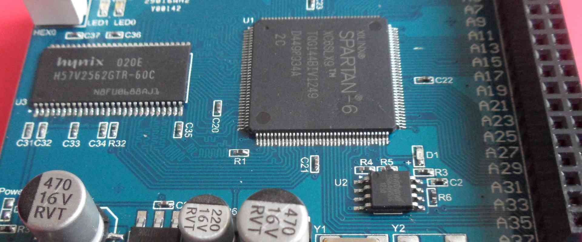
A PCBA features different copper lines and traces. These boards can be very tiny, but they are very effective. Electronics PCBA is an aspect of the electronic processing industry. It involves mounting various electronic parts on a blank circuit board.  PCBA electronics perform several functions and are ideal in most applications.

Applications of PCBA Electronics

A PCBA board is ideal for use in several applications. Most devices come with PCBA. Computers, smartwatches, smart phones, etc. feature PCBA boards. To date, PCBA electronics are commonly used in most industries. As technology keeps advancing, PCBA electronics will continue improving. Electronic PCBA will always be the core of all electronic devices.

Even in todayโ€™s world, PCBA electronics play a significant role. A PCBA board will always be useful in several industries. Letโ€™s discuss the applications of PCBA in todayโ€™s world.

Consumer electronics

In this field, PCBAs are largely used. Most of our home appliances canโ€™t function without a PCBA board. Consumer electronics are devices we use in our daily lives. Examples include microwaves, televisions, radios, and smartphones. The manufacturing of these appliances requires the use of a PCBA board. The advent of PCBA electronics has enabled the production of small and complex devices.

Record keeping gadgets, computer devices, mobile phones, and entertainment systems all feature PCBAs. Since PCBAs are mechanically and electrically stable they are suitable for these devices.

Automotive industry

PCBA electronics are common within the automotive industry. This circuitry provides a lot of benefits for this industry. The production of vehicles solely depends on PCBA electronics. Some car parts like car headlights feature PCBA boards. It is evident that this circuitry has had a positive impact in the automotive industry.

The regulator systems in vehicles feature PCBAs. Navigation gadgets also feature PCBA. Without doubt, this board has added a lot of benefits to this industry. From improved safety measures to high-performance automobile parts.

Industrial application

The production of both heavy-duty and light-duty machines involves PCBA. In the manufacturing industry, most machines feature PCBA. These machines make use of high-frequency and high-speed PCBs to ensure smooth operation. Since most of these devices are exposed to harsh conditions, they feature high-performance PCBA boards.

These boards can tolerate high mechanical stress and corrosive chemicals. Devices like a thermometer, AC converters, hydraulics, and pressure pumps all feature PCBA boards.

LEDs

Light emitting diodes have improved due to the advent of PCBA boards. These days, LED producers utilize PCBA electronics to design various lighting systems.  LED PCBs are now available in the market. This lighting system, LED, is known for its functionality and little power consumption.

Medical devices

PCBA boards are suitable for the production of medical devices. There is a great improvement in the medical industry as a result of PCBA electronics. Medical practitioners make use of some machines to diagnose ailments in patients. These machines feature PCBA electronics. Most medical devices canโ€™t exist without PCBAs. Ultrasound machines, CT scanners, and X-ray devices among others feature electronics PCBA.

Steps in PCBA Process

PCBA BOARD

The PCBA process is an important aspect of the PCB industry. This process involves some steps. The manufacturer must carry out these steps carefully.

Prepare the surface of the PCB

This is the first step in PCB assembly. It involves preparing the board surface for the fabrication of the assembling of the electronic components. You have to choose the right board size and get it ready.

Part placement

This step involves placing the components on the board. The pick and place machine is ideal for this purpose. In those days, manufacturers carried out this step manually. They make use of tweezers to place the components on the circuit boards. This method had so many errors because humans are likely to make mistakes.

This led to the invention of the automatic pick and place machine. With this machine, you can be sure of accuracy and precision. The pick and place machine picks the component and places it in the right location. This machine needs to be programmed before you begin with this step. You need to program this machine for you to place the components at their right locations.

Soldering

Soldering is a step that involves applying solder paste to the circuit board. A solder paste comprises flux and solder. This mixture helps to melt the metal and join it to the surface. This process is technical and as such, will require a solder paste printing machine. Some manufacturers use the reflow soldering technique wave soldering.

Cleaning

After soldering, you will need to clean the unwanted materials on the PCBA. A fiber brush will be of great use for this purpose. This brush will get rid of any unwanted material on the board.
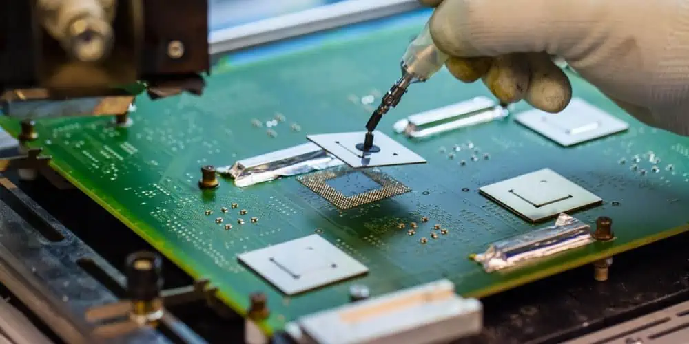
Inspection

Errors may likely occur during the PCB assembly. This step helps to detect any error during the assembly of the PCB. Errors can result in no connection or misalignment. Therefore, inspection is very important. It helps to prevent unnecessary expenses in the future. Several inspection techniques are employed in this process.

Techniques of PCBA Electronics

PCBA contract electronics manufacturers employ two main techniques for PCB assembly;

Through-hole Technology

This is an assembly process in which holes are drilled into a circuit board. The manufacturer drills holes into the board. Then, these holes create ways to attach electrical components. PCBA manufacturing company employed this technique first.

Through-hole technology provides a stronger bond between the circuit board and the component. This technique enables more reliable assemblies. The first step in this technique is to drill holes. After that, you put the leads in the hole. The manufacturer then applies solder pastes to ensure the components stay firm.

Surface mount technology

This technique has gained popularity in the PCB industry due to its benefits. PCBA manufacturers prefer surface mount technology to through-hole technology. SMT involves using a machine to mount electronic components on a circuit. This technique is highly flexible and enables greater connection densities.

For this technique, the manufacturer will have to prepare the board first. After this, you use a pick and place machine to mount components on the board. The PCBA manufacturer heats the PCB at the right temperature in an oven. This technique is more convenient and reliable.

Inspection Methods for PCBA Electronics

Inspection and quality control are the final stages of PCBA. This aspect is very important in PCBA. In PCB assembly, there are different inspection methods.

X-Ray inspection

This inspection method is very technical as it involves the use of X-rays. You will use X-rays to check the PCB layers to detect any inconsistencies. If the X-ray detects any, there will be rectification. This inspection method is ideal for complex circuit boards.

Automated optical inspection

AOI incorporates the use of a machine. The automated optical inspection machine features several cameras. These cameras will scan and view the boards from various angles. The cameras will then detect any errors. This machine is common among PCBA companies.

Visual inspection

The visual inspection method involves using a manual process to inspect PCBs. This method is more suitable for inspecting a small quantity of PCBs. Visual inspection canโ€™t be ignored in PCB assembly. In as much as it has its own limitations, its benefits canโ€™t be overlooked.

What Does a PCBA Comprise?

FULL PCB MANUFACTURING Quote

A manufacturer mounts electrical components on the surface of a circuit board to produce a PCBA. A circuit board assembly comprises different electronic components.

Capacitors

Capacitors are electronic components on a circuit board. This component holds an electric charge and then releases it when there is a need for more power. Capacitors collect opposite charges on two layers to achieve this. This electronic component functions as a rechargeable battery. It saves electrical energy and then provides this energy when needed.

Resistors

These are electronic components that regulate the electric currents that go through them. They also control the voltage in every component they are connected to. The absence of resistors in PCBA will lead to overloading. Without resistors, other components canโ€™t handle the voltage. Resistors discharge electric power as heat. This component withstands the flow of current in a circuit board.

Transistors

Transistors serve as the backbone of modern electronics. They are like the building blocks of todayโ€™s electronics. These components play a vital role in PCBA electronics. They act as insulators and conductors. These semiconductor devices can serve as amplifiers and switches. Transistors can function at lower voltage supplies without a filament current.

Diodes

Diodes are electronic components that enable the flow of current in one direction. They serve as one-way switches. They allow the flow of current in one direction while restricting current flow in the opposite direction.

Inductors

These electronic components save energy in a magnetic field anytime an electric current flows through them. Inductors block alternating currents and enable direct current to flow. These components can be used alongside capacitors to design tuned circuits.

It is very important one understands the functionality of these electronic components. They all make up a printed circuit board assembly. PCBA electronics exist due to these components. Electronic components play a vital role in PCB assembly.

Advantages of PCBA Automation

Printed circuit boards are the core of all electronics. Todayโ€™s electronics canโ€™t exist without a PCBA board. As technology continues to advance, PCBs are now easier to design. All thanks to automation and machines. They have made the production of PCBA electronics a much easier task.

In the past, electronic PCBA was designed manually. This led to less consistency and slower production. PCB assembly automation offers various advantages to sectors and businesses. Below are some advantages of PCBA automation;

Consistent quality

Automated machines can perform the same task continuously without errors. They have helped PCB manufacturers design better and more accurate circuit boards. Automation helps you to get the accurate design for all circuit boards. With this advancement in technology, you can be assured of consistent quality.

Lower cost

The use of machines has contributed largely to the PCB industry. Manufacturers donโ€™t have to spend so much on production costs again. The majority of SMT assemblers make use of software for PCB assembly. These applications are used before the actual PCB production. Doing this minimizes the risk of delays and errors. Automated PCBA also results in financial savings since the task will require fewer employees.

Reduction in error

Errors are most likely to occur during PCB assembly. The PCBA process is a task that requires carefulness and attention. While humans can make mistakes, these machines are less likely to make errors. These machines are designed to carry out certain tasks delicately and repetitively. Automated machines can assemble more boards in less time.

 Ideal for mass production

PCBA automation can minimize the costs and time for producing PCBs. Therefore, PCBs can be produced in higher quantities. Automated services will help you deliver consistent boards in a timely manner.

Short product development cycle

While hand-assembled boards may take a longer time to design, automated boards take a shorter time. An automated PCB assembly service will assure you of high-quality boards.

How to Choose a Good PCBA Electronics Company

For all PCBA companies, staying at the top of the game is important. That is why these companies keep up with PCBA capabilities. Before choosing a PCBA electronics company, it is important you take some factors into consideration. There are several PCBA electronics companies out there. However, it is vital you choose a professional PCBA company.

Experience

This is a great factor you need to consider. Experience is very important. You definitely want a company that has the required experience for your PCB assembly. The assembly of PCB is a daunting task that needs attention to detail. You will have to make an inquiry about the company you are opting for. How long has this company been existing? How many firms have they collaborated with and which? What kind of techniques do they employ for their PCB assembly? It is important you ask these questions.  

Customer support services

The customer service of the company you are opting for also matters. The support system of a PCBA company should pay attention to customerโ€™s needs. This system takes your matter seriously and answers all your questions. For a great PCBA, you need a company with great customer support services.

Skill

This is another factor you need to consider. The employees of a PCBA company need to know what PCB assembly is all about. It is important you make some detailed inquires about the employees of the company. This will help you to choose rightly.

Testing and inspection options

The type of testing and inspection methods a PCBA company employs determines a lot. To achieve quality, proper testing and inspection technique is vital. Ensure you know the type of testing and inspection methods the company you are opting for employs. Some companies use automatic optical inspections while some use X-rays.

Cost

Cost will determine a lot of things. In the end, you want quality PCBA boards. These boards cost a price. However, some factors determine the cost of a PCBA. The quantity you order and the cost of shipping influence the cost of a board.

If you make a large order, you will pay more. The type of technique used for your board also matters. The cost of through-hole and surface mount technology differs.

Quality

A good PCBA company will offer quality products. You need to evaluate the quality of products offered by these companies. Ensure that the quality of the electronics PCBA meets your requirements. You should also make an inquiry about the type of equipment these companies use.  Also, check the reviews and feedback of customers.

Certification

Some companies work in line with the necessary standards. Ensure your PCBA Company has the necessary certifications. These companies operate according to the standard regulations and rules. Ensure you go for a company that has the right certification.

PCBA Capabilities

Components sourcing

The majority of PCBA manufacturers expand their network. The component sourcing is one the services offered by this company. This service has several benefits, one of which is line efficiency.

LED PCB assembly

LEDs are common in most electronics produced today. PCB manufacturers can now design a LED PCB that emits light anytime it is connected to a power supply. Since LEDs offer high-intensity and better quality, they are attached with PCBS. Flashlights, operating room lighting, and street light feature LED PCBs.

Through-hole assembly

This type of assembly is ideal for THT components. Through-hole assembly requires manufacturers to fix components on board through the holes.

BGA assembly

Ball grid array (BGA) features several bumps at the end part of the tube. These bumps provide an interconnection between the body and the base.

Prototype assembly

Some PCBA manufacturers offer fast prototype assembly. These services save time to market. Prototype assembly provides manufacturers with the opportunity to adjust and rework the circuit board.

Frequently Asked Questions

Why is PCBA electronics important?

Electronics PCBA is vital in the PCB industry. In todayโ€™s world, most electronic devices feature PCBA electronics. This board helps to improve the efficiency and productivity of electronic devices. Without a PCBA board, an electronic device canโ€™t function. These boards serve as the backbone of most electronic devices.

What services do PCBA companies offer?

PCBA companies offer a lot of services. This includes SMT and through-hole technology and completed box build assembly. These companies also offer contract electronics.

Conclusion

PCBA electronics plays a vital role in electronics manufacturing. A PCB is different from a PCBA. Printed circuit assembly involves the mounting of electronic components on boards. PCBs are a blank board. These electronic components make them ideal for use in several applications. As technology continues to advance, the need for PCBAs continues to increase. Contract electronics companies also ensure the production of PCBA boards.

Introduction to Circuit Assemblies

Circuit Assemblies

The process of learning about circuits and learning how to assemble them is quite easy. Therefore, this guide will be of immense help to a beginner in circuit assembly. We will discuss the basics of electricity and how it relates to a circuit and we will also touch on the materials needed to assemble a circuit. This foundational knowledge will give you an edge when you progress to much more advanced stuff.

What is Circuit Card Assembly?

Circuit card assembly involves several stages. Circuit card assemblies are the complete PCB after the assembling of every component. A printed circuit board has no electrical components. Circuit card assemblies are the complete board assembly. The assembling of a circuit board requires both active and passive components.

Circuit card assembly is also the same as printed circuit board assembly. These terminologies are widely used in the PCB industry. The process of circuit card assembly involves several stages.  Circuit card assemblies involve using schematic capture tools or CAD software.

Circuit card assembly involves connecting the wirings of PCBs with the electronic components. The traces in the copper sheets of PCBs will form the assembly.

Ways to Create Circuit Card Assemblies

circuit assembly

There are several ways to create circuit assemblies. So, it is important one pays attention to details during the process of circuit card assemblies.

Plated through-hole technology

This method involves mounting the components on the circuit board by putting their leads via the respective hole. The circuit board already has drilled holes. This makes it easy to assemble the circuit boards with the components. A thin layer of copper covers the holesโ€™ inner wall. With this, the whole area of the inner hole becomes conductive.

This method has its benefits and disadvantages. PTH might fail due to the cracks in the copper that plates the inner hole. There are ways of testing the reliability of PTH.

Surface mount technology

Surface mount technology is a common way of creating card assemblies. This method is mostly preferred in the PCB industry. Most circuit card assembly manufacturers prefer SMT due to the benefits it offers. ย SMT refers to the process of using automated machines to assemble electronic components on a circuit board.

Electro-mechanical assembly

This method utilizes cable assembly, molded plastics, wire harnesses, and looms. These things help to assemble electronic components on a PCB. Effective circuit assemblies help to ensure the smooth function of electronic devices.

Steps in Circuit Card Assembly

Printed circuit boards have been the backbone of most electronics devices. These boards offer connectivity for the components of an electronic device. A circuit card assembler ensures that the circuit board is properly assembled. Circuit card assembly involves step by step process to achieve. However, this step may vary based on the method of PCB assemblies.

Schematic design

This is an important stage in circuit card assembly. You should design a schematic that serves as a guideline for the whole circuitry. A schematic is a roadmap that features symbols that represent the entire circuit board. As a circuit card assembler, you should create a schematic. This will help you tackle any problem that may arise in the future.

Board design layout

After creating the schematic, the next thing is to lay out the board design. This involves translating the schematic into design software. The assembler will then export it into an acceptable format. This format will help the production stage of the circuit board.

Manufacturing & Assembling the PCB

This stage involves creating the board. In circuit card assembly, there are different methods. An assembler can either use plated through-hole technology or surface mount technology. The choice of method to use depends on the board’s specific requirements.

Inspection and testing

This is the last stage of the assembly process. It is important you test the circuit board to ensure it works perfectly. There are three different methods of inspecting circuit boards.  Visual inspection, X-ray inspection, and Automatic optical inspection are these methods. These methods have a similar purpose but use different ways to carry out inspection.

The visual inspection only inspects the soldered connections. The AOI machine uses high-resolution cameras to test circuit boards. For complex PCBs, an X-ray inspection will take place.

Circuit Assembly Design Basics

All electronic devices feature circuit assembly. Even the smallest electronic device has circuit assembly. It is important we understand the basics of circuit assembly design. Irrespective of the type of circuit board, all circuit boards feature the layers below;

Substrate

 This is the foundational material for circuit assembly. The substrate provides the circuit board with rigidity. Fiberglass is the primary material for the substrate layer of any circuit board. Asides from flexible PCBs, most boards use fiberglass for their substrate.

Copper

Printed circuit boards feature a layer of copper foil. The manufacturer laminates the copper foil to the board using heat. The number of copper layers for a PCB depends on the type of PCBs. For example, single-sided PCBs require a layer of copper on one side of the board.

Solder mask
The yellow or green color of circuit boards is a result of soldermask. The manufacturer places the soldermask on top of the circuit board. This helps to insulate the copper layer. Doing this will prevent the copper from any contact with other metals on the board. The soldermask layer helps the manufacturer to solder the components to the appropriate places.

Silkscreen

The silkscreen is the final and uppermost layer of all circuit boards. This layer features components in symbolic or textual form. It helps engineers to have a better understanding of the board. The silkscreen adds symbols, letters, and numbers to the board. This helps to understand the functions of various LEDs and pins.

Manufacturing Steps of Circuit Card Assembly

circuit card assemblies

A circuit card assembly involves several steps.

Solder paste stenciling

The CCA manufacturer applies a solder paste to the circuit. This process involves applying solder paste on specific portions of the board. This portion holds several electrical components. Various tiny metal balls make up the solder paste. Tin accounts for 96.5 percent of the solder paste. Other substances used for solder paste include copper and silver.

The manufacturer must apply the right amount of solder paste at the appropriate spots. You can utilize various applicators to spread paste in the right locations.

Pick and place

The pick and place process involves using an automated machine. Here, the manufacturer puts various SMDs and electronic components on the PCB. You can pick and place components on circuit boards using either automated or traditional methods. Manufacturers place components on boards using a pair of tweezers in the traditional method. In the automated method, manufacturers use machines.

Reflow soldering

Manufacturers need to solidify the solder paste after the components have been rightly placed. In this process, the boards get to a conveyor belt. This belt passes from a large reflow oven. This oven features heathers with various temperatures.  The heathers change the solder into a paste using heat. The conveyor belt goes through coolers. This will help to solidify the solder paste. This process enables all components to be firm on the board.

Quality control

This is stage is very important. Manufacturers have to check the board for any errors after they have mounted the components. Here, manufacturers inspect the boardโ€™s functionalities. Some boards are poorly connected during the reflow process. Therefore, there can be some connection problems in these boards. It is important to inspect the board for any errors.

What is a Circuit?

First, letโ€™s discuss the way electric current works. Electricity needs to flow before it can perform any activity. Electricity cannot flow through all types of materials. It can only flow through certain materials that can conduct it. An example of this is copper wire.

Electricity automatically flows from a point of high voltage to a point of low voltage. Once you put a conductive route from a high voltage to a low voltage electric currents can flow on that route. You can test if the route is flowing with electricity by inserting an LED to serve as a load. The electricity should light up the LED.

Electricity has two poles or sides. This is commonly found on batteries and some sockets with two or more holes. These poles are usually called terminals. They are negative (-) and positive (+).  The purpose of these two different poles is to create a point of high voltage and a point of low voltage for electric current to flow

As such, in any electric current transmission, the positive pole has a higher current than the negative pole. The volts in the negative pole are often zero and the positive pole contains as many volts or current as it needs to supply. This explains how an electricity source works. For instance, generators and batteries generate electricity and transmit it towards the positive side. The negative side then sucks in electric current back to keep the electricity flowing and active.

This path through which electric current moves back and forth is what a circuit is. A circuit could be very simple like connecting a Light Emitting Diode to both poles of a battery.

Components of an Electric Circuit and Network

These are the main components of an electric circuit:

  • Node: A node is a junction or point where at least two circuits elements (capacitors, resistors, inductors, and so on) meet.
  • Branch: A branch is the section of the circuit amid two junctions. In a branch, you can join one element or even more and there will be two terminals.
  • Loop: A loop is a path in a circuit that contains more than two meshes. It is the enclosed path of a circuit. Thus, a loop can contain meshes, but a mesh cannot contain another loop.
  • Mesh: A mesh is like a loop but it does not contain another loop.

Basic Electronic Components that are necessary for circuit assembly

FULL PCB MANUFACTURING Quote

There are some rudimentary electronic components that you will make use of when assembling electronic circuits. Some of these components are diodes, integrated circuits, transistors, capacitors, and resistors. We will briefly examine the functions and uses of these electronic components.

Resistors

A resistor is a major component used in the circuit assembly.

A resistor as the name suggests adds resistance to the electric current flowing in a circuit. Resistors represent a different value that reflects with a color code. The unit of resistance is Ohms and Omega is its symbol.

When you draw a circuit on paper, the resistor is symbolized with a pointy squiggle that has a value written beside it.

You can measure the resistance level of a resistor. You can use a Graphical Resistance Calculator to measure it. Each resistor usually has a different wattage rating. You will find one-quarter watt resistors in DC circuits.

Diodes

A diode is a polarized component. The electricity in a diode flows in one direction. This offers an advantage if you want electric current in a circuit to flow in a particular direction.

A ring on the diode is a symbol that indicates that one side is connected to a GND (Cathode) and the other terminal side is connected to Power (Anode) or VCC.

Transistors

A transistor is a component that receives a small amount of electric current at its base pin and augments the current to the extent that a larger current can flow between its emitter pins and collector. The electric current that flows through the two pins is proportionate to the number of volts that are applied to the base pin. These perform the role of a switch that does not have a moving part. A microcontroller can be used to control this.

There are various kinds of transistors. PNP, MOSFETS, and NPN are some common examples of transistors.

There are three parts of a transistor. The first is the Base. The base serves as the lead which is used to activate the transistor. The second and third are the collector and emitter. The collector serves as the positive lead while the emitter serves as the negative lead.

Potentiometers

A potentiometer is a type of resistor which can vary. A slider or a knob can vary the resistance. These mechanisms are usually employed to regulate the brightness and volume of lights. Knob potentiometers and slider potentiometers are similar to transistors. A potentiometer has three terminals.

Integrated Circuit (IC)

This is also called a microchip. An IC can be described as a largely diminutive form of a very large circuit. It contains millions of tiny transistors and resistors. It receives input and gives out output through the several terminals the IC has. To understand how a specific IC operates, you can look up its datasheet.  

There is no specific design for an integrated circuit. It can be made into several sizes and shapes. Beginners will be more involved with DIP chips. These chips are built with a pin for through-hole soldering. SMT (Surface Mount Technology) chips are used in the more advanced electronic circuit assembly.

Light Emitting Diode (LED)

An LED is a device that converts electricity into light. A light-emitting diode is also a semiconductor. It is more durable when compared to an incandescent light bulb. An LED is not restricted to a kind of color. They are very efficient and they produce more light from the electric energy and little heat.

If you want to power several LEDs in a circuit, use the parallel circuit method. As tempted as you may be, do not wire them in series. This is because the voltage will keep dropping after it reaches each of the LEDs until the electric current left is insufficient to sustain the lit LEDs. If you use the parallel circuit method, make sure the LEDs you use all have equal power ratings. This is because the ratings vary with the color.

Switch

A switch simply refers to a device that breaks a circuit mechanically. When you trigger a switch, it either closes the circuit or opens the circuit. This depends on the kind of switch in the circuit. The switch that opens or closes a circuit is the simplest form. Advanced switches will perform the function of opening a connection while simultaneously closing another when you activate the switch. This advanced type of switch is a single-pole-double-throw switch (SPDT).

There are several varieties of switches which include SPCO, SPST, 2P6T, or DPDT and DPST.

Battery

A battery helps to convert chemical energy into electrical energy. A battery contains specific chemicals that react with each other in a particular way to create electricity. Every battery has three parts, the cathode (+ positive side), the anode (- negative side), and an electrolyte. You connect the anode and cathode to an electric circuit.

The reactions of the chemicals in the battery lead to an accumulation of electrons at the anode. This makes the voltage at the anode high and the voltage at the cathode at zero. Thus the electrons will flow from a high voltage point to a low voltage point. That is from the anode to the cathode.

Batteries are symbolized in a circuit diagram by lines of dissimilar lengths that are serially arranged. There are further markings that can be attached to the symbol to signify ground, voltage rating, and power.

Breadboard

This component can test and design circuits. Breadboards are commonly used by engineers. When using a breadboard, there is no need for you to solder components and wires to construct a circuit. A breadboard makes it convenient to mount and reuse components. Also, since the components are not fixed through soldering you can easily maneuver the design of your circuit at any point during assembly.

Breadboards contain a collection of conductive metal clips enclosed inside a white plastic box.  The plastic box has several holes that are specifically arranged. The average breadbox layout consist of two kinds of a region known as strips. They are socket strips and bus strips. The bus strips often serve as a means of power supply for the circuit. There are two columns in bus strips, one column for ground and the other for power voltage.

Multimeter

Just as you would use a tape rule to measure cloth, a ruler to measure length, or a watch to measure time, this is an easily accessible tool that can measure electric energy or electricity. A multimeter can measure a lot of things apart from electricity. It usually has a knob that you can use to choose the type of measurement you want.  

Platforms Useful for Assembling Circuits

Arduino

The Arduino platform is an open-source program that assembles circuits and build electronic projects. This platform has a microcontroller (a microcontroller is a tangible programmable circuit board) and software you can run on your PC. This software is for the purpose of writing and uploading computer code to the microcontroller.

Autodesk 123D

The best way to get started with Arduino is to write a simple project and figure out the right code to run with it. If the Arduino platform is inaccessible for you and you want a quicker way to assemble a circuit or you want to expand your horizon and learn other methods, you can give 123D circuits a try.

123D Circuit is an online platform that allows you to construct and test run online Arduino circuits. It also allows you to debug the code you used, check the wiring, and try out different circuit constructs. This is awesome too for beginners in the use of Arduino and experts in search of flexibility.

Frequently Asked Questions

Why does a circuit assembly fail?

Circuit assembly might fail due to certain reasons. Poor design, trace damage, physical damage, and component failure are reasons a circuit may fail.

Can I repair circuit cards?

Yes, you can repair circuit cards depending on the kind of damage. Before you can repair your circuit cards, you need to know the cause of the damage.

Conclusion

Circuit assembly involves several processes. The assembling of circuit cards is an important procedure in the PCB industry. In this article, we have reviewed important facts you need to know about circuit assembly.