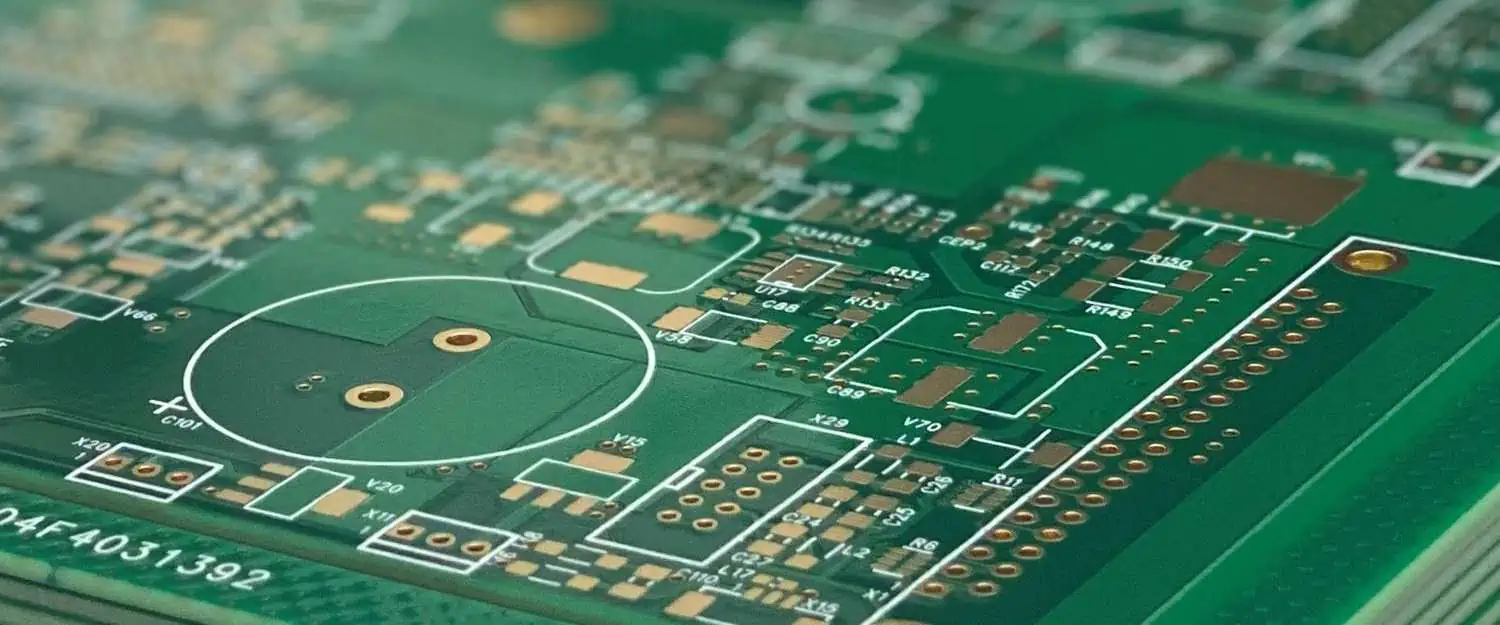
The increase in the demand for PCB miniaturization has resulted in the design of very complex PCB layouts. Complex PCB layout usually involves inserting holes in BGA pads. A via in a circuit board is used to join pads, polygons, and traces on various layers of the board. It is a core part of a PCB as it ensures proper connection in the board.
Vias offer connections between several layers of a PCB. Multilayer boards usually feature at least two layers of copper. Vias make it possible to fabricate a PCB with more than a layer of copper. There are different types of vias. Our main topic in this article is capped vias. Capped vias enable the design of via in pad due to their flat surface.
A capped via is a type of via in which plating is included over the via hole. In such a case, the surface becomes metalized with cap plating thickness. Capped via technology is crucial for the fabrication of high density interconnect boards (HDI). This via features hole filling with resin. The design of capped vias helps in improving the density of the interconnection in PCBs.
The two primary technological solutions are resin via filling and copper via filling. The capped vias have hole filling with resin which helps in improving interconnections in HDI printed circuit boards. These vias integrate through holes’s space as SMD assembly points. The capped via technology comprises filling the holes after they have been plated. The copper thicknesses are usually >25µm. However, the copper thickness may be defined according to the customer’s specifications.
The resins integrated for “capped vias” feature some insulation properties. Also, the dimension of this resin varies according to changes in temperatures and as such, they are treated with heat for the consequent hardening. The resins are first planarized and a layer of copper covers them. The copper layer thickness is at least 15µm.
PCB manufacturers can apply this technique to realize various types of printed circuit boards. Also, these various applications is a reason for strong expansion.
Phases of filling holes in PCB
There are two distinct phases for filling the holes with resin. In the first phase, vacuum and variable pressure fill up the holes. This enables the proper filling of the holes without any risk of having space in the resin. The second phase requires cleaning the surface of the panel to get rid of any excess resin, and as such, improving its subsequent planarization.
Regardless of the final technology you selected, a mechanical brushing process referred to as planarization helps in removing the resin. Planarization is usually done after polymerization has been completed. Also, planarization uses some particular machines that integrate cup brushes.
The aim of planarization is to get rid of the excess resin and enable an even surface. This process is crucial for over-plating of the filled vias with copper in order to enable soldering of electronic components.
The “capped vias” technology is crucial in today’s PCB. This technology has helped in creating compliant circuit boards to market. Also, it has helped to meet some regulations standards, especially those associated with the growing HDI technology demand.
Why is Capped Via Technology Crucial in PCB Fabrication?
The rising demand for the miniaturization of printed circuit boards, particularly in some industries has, led to the design of complex PCB layouts. These layout process often involve embedding interconnecting holes into the Ball Grid Array (BGA) pads. Therefore, these same pad help to realize the internal circuitry of the printed circuit board and its typical SMT use. The benefit of this is evident in the reduction of the circuit board size. However, the limitation becomes evident in the complexity of the SMT mounting procedure. Also, there is the possible reliability lacks into printed circuit board assembly (PCBA).
A good amount of the epoxy glue can pass through the hole when there hole in a SMD pad. This can cause a void (dry joint) and as such, have a negative impact on the component or result in a sudden break of the connection of components in the board.
Two different approaches can be used to solve these kind of problems as earlier mentioned. Capped vias and filling copper are these two approaches. The filling copper technology involves the depositing extra copper in the hole, until you have been able to reach the requested filling percentage. There is always a dimple to avoid compromising the pad’s thickness. This is because the deposition of copper, even in minute amount, impacts the pad.
Capped Vias: A solution to complex PCB manufacturing
While some SMD components don’t need any planarity some components do. In such a case, the capped vias technology is last resort. This technology plays a significant role in the manufacturing of complex printed circuit boards. It involves filling the hole with a good amount of resin requires and then plating it. A thin copper cap is deposited into the pad. One of the benefits of capped vias technology advantage is how it preserves interconnections generated by the hole. Also, another benefit of this technology is the perfect planarity of the pad which enables easy mounting of each component.
There are other cases where the capped vias technology can be integrated. It can be integrated in buried vias rather than laser vias (BGA pads). Some micro-break at every corner can affect the buried vias plating when you apply the SBU technology. This occurs due to the mechanical processes the PCBs are exposed to
In this case, the risk is evident. This includes the unreliability of the PCBA and the malfunctioning of the interconnections caused by the buried via. Resin is used in filling up the buried vias in order to prevent this possible problem from occurring. In fact, this process makes the via robust and as well preserve the desired performance of the board.
Everything keeps evolving. Things change and transformation is necessary in technology. With the constant evolvement and increasing advancement in technology, the PCB design and manufacturing processes keep getting better. As a result of this, industries need to keep up with this pace of innovations.
The printed circuit board industry isn’t an exception to this innovation. The PCB technology occupies a vast and dynamic space. The integration of vias in circuit boards have become popular because of the development of modern electronic devices and their applications. Vias are crucial for creating interconnection between PCB layers. These holes play a foundation role in ensuring interconnectivity between circuit board layers.
Also, this technique is useful in multi-plated and complex layouts. So, what are the benefits of capped vias in PCB design?
Enhanced thermal dissipation
Choosing the capped via technology for a PCB design helps to include extra capping to the manufacturing process. The efficiency of these vias worth the cost of a complex PCB design project. High power surface components usually feature thermal pads. Capped vias are a better option in this case compare to traditional routing styles.
Furthermore, the components of via offer support to heat management within the pads. The copper area become bigger when vias are dropped in from one side of the board.
Enhanced PCB density
Capped vias are ideal for use in high density interconnection boards. These vias enhance the density interconnection of complex boards. The circuitry requirements of a PCB layout will determine the suitability of capped vias. Capped vias technology is crucial for complex circuit boards.
Traditional circuit board routing techniques don’t offer support to the rising demand for PCB chips miniaturization. However, capped vias does. The vias’ position on the mount surface is a crucial factor to consider. However, this helps in preventing any issues for complex projects. Capped vias are a perfect option in PCB designs where space is crucial. As regards improving density and enhancing performance, capped vias are an ideal choice.
Improved performance capability
One of the benefits of integrating capped vias technology in PCB design is increased voltage capability. Vias feature resistance and inductance characteristics which in turn impact the flow of current. These variables can affect the functionality of a circuit board. Capped vias allow shorter paths and increase the performance of the board. Capped vias help to enhance the voltage of vias.
Additional treatments are required on vias to increase their thermal performance. These treatments include capping, filling, covering, or plugging. Integrating any of these processes help to get rid of many assembly issues like short circuit or solder wicking. With a proper via treatment, it is possible to get rid of rework or troubleshooting.
Plugging prevents solder flow or wicking when soldering. Filling is a good option of via treatment. PCB fabricators use non-conductive epoxy to fill encroached paste. Some PCB fabricators make use of conductive paste to fill micro-vias to improve conductivity.
Conductive filling enables the transfer of signals form one part of the board to another. Therefore, this helps to improve the thermal properties.
Conclusion
Capped vias feature several benefits which include the reduction of EMI, improved routing density and enhanced thermal conductivity.
The capability of vias to carry signals properly is equivalent to the successfully designed Circuit board in consumer electronics along with all other businesses that depend on the well-manufactured circuit boards. The conduits known as vias are what allow electrical signals to move across a PCB’s layers.
Manufacturers frequently add a conductive metal layer, usually copper into the substrate of a PCB to link the layers when the appropriate holes and layout are drilled. Copper plating works well for several purposes. Nevertheless, plated thru holes may additionally be filled with much more conductive material including copper for any application that generate a lot of heat or a lot of current. This configuration produces what are known as the copper filled via.
Electroless nickel immersion gold is proven to be among the most common surface finishes present on the marketplace today for businesses whose applications have become more demanding or/and those desire the newest in Circuit board. Due to the fact that ENIG finishes are lead-free, they are also a wise choice for businesses who wish to adhere to the RoHS directive 2002/95/EC. The use of some hazardous compounds in electronic products and gadgets is restricted by this EU rule.
Every PCB finish has disadvantages. Ball grid array components and other objects linked to the Circuit board run the actual danger of experiencing ENIG black pad issues with ENIG finishes.
However, ENIG finishes cannot be reworked, making the issue of black pad one that must be carefully handled. Otherwise, a whole product might become unworkable, costing money to recall and causing lost sales and disgruntled consumers.
Black pad can be described as a coating of the dark nickel surfaces that has been deposited on your PCB’s exposed portions. Because of the excessive usage of phosphorous during the process of gold deposition, this layer develops throughout the manufacturing process.
This electroless nickel has oxidized and corroded, as shown by the black pad of the metal. The assembly process takes place when different metal components are joined, but as this corrosion gets worse, it slowly spreads.
Because of increased nickel oxidation and increased gold thickness during manufacturing, there is inadequate solderability and improperly constructed soldering connections. The term “black pad” refers to the solder connections that quickly shatter under pressure to reveal rusty nickel underneath.
What Does ENIG Black Pad Mean?
This ENIG black pad controversy in the Circuit board sector may be unmatched by any other issue. Black pads are poorer connections that happen at the nickel and solder interface, to put it simply. Although some estimates place the prevalence of such a phenomenon at far less compared to 1 or 2% of the ENIG PCBs, many industry experts believe it to become very rare.
Nevertheless, because the black pad issue is typically not identified until the assembly process has started, it can be expensive to rectify as well as correct its post-manufacturing stage.
Why Does ENI Black Pads Occur?
A high content of phosphorus
The significant pass phosphorous level in gold deposition method typically results in ENIG black pads because of soldering and reflows.
Phosphorus diffuses through into nickel that causes its oxidization when there is an excess of it. This procedure separates the gold from the nickel, preventing the development of an adhesive bond.
Thus, this may result in dependable solder junctions delaminating and breaking, which might result in electrical shorts on circuit boards.
Corrosion from Gold Deposition
The popular ENIG surface finishes used in PCB manufacturing need the gold deposition technique, which is a vital step in the overall process. Yet if you don’t handle it right, this procedure might also result in the development of ENIG black pads.
Use of vigorous gold baths is among the reasons that enig black pads develop during the deposition of gold. The nickel bath method has the potential to quickly corrode nickel, resulting in the development of black pads.
This creation of ENIG black pads may also be influenced by the excessive gold thickness. When the common nickel substrate treatments contain excessive gold on them, severe galvanic hyper-corrosion as well as the eventual creation of ENIG black pads might result.
Employ gold having a thickness of about 2 to 4 μin, as required by the specification of the IPC-4552 ENIG, to avoid the creation of black pads.
Brittle fracture
Materials that are under tremendous stress might fail in a way known as brittle fracture because they lack the flexibility that can withstand the tension and break down rapidly without any warning or notice.
Typically, the surface of the PCB will have an ENIG black pad due to this failure.
This transformation of tin to nickel is the most frequent reason for brittle fracture. These metallurgical bonds are compromised by the small coating of phosphorus which remains after this transition.
In addition, brittle fractures could be brought on by temperature stress, shocks, and vibrations. Whenever this occurs, the nickel becomes broken, which can result in the electrical shorts.
The Development and Possible Harm of ENIG Black Pad
The composition of the plating solution and temperature when the process of chemical displacement process is on are the two main factors that affect the quality of the nickel coating. The most important thing is how you handle this acid gold water.
This plating layer gets formed during the process of electroless plating by an autocatalytic interaction between nickel salt and hypophosphite on the surface of the pad.
The amount of phosphorus in the finished product is calculated with the use of this processing assist. This industry standard for the phosphorus ratio in the deposition of chemical nickel was found to be between 7 and 10% in several investigations.
However, this proportion will deviate from the ideal range when the temperature changes or composition of the solution’s isn’t maintained under strict control. The coating is going to be more vulnerable to hyper-corrosion through the erosion of the acidic gold waters when the phosphorus content ratio is low. The lack of phosphorous in metallic ion concentration plating prevents the reaction of chemical substitution from occurring effectively during the process of gold immersion, which results in the hyper-corrosion.
When the gold coating develops a substantial number of fissures, it will be challenging to remove acidic residue. Its electroless nickel surface will corrode and also turn black if exposed to acidic water.
On the contrary hand, when the phosphorus levels are excessive, the produced coating’s hardness would rise noticeably, limiting its capacity to be welded and impairing the dependability of the batch solder junctions.
Prevention of Black Pad
About black pad, industry experts unanimously concur that it couldn’t occur at a worse location in the research and manufacturing paths of electronic goods and components.
As a result, it becomes vital for PCB suppliers and manufacturers to prevent ENIG black pads. Of course, understanding that excessive phosphorous levels are the source of ENIG black pad is not the same as properly regulating those levels throughout the production process. In order to prevent black pad concerns with the ENIG finishes, selecting us as your provider is probably the wisest move you can make. We are entirely devoted to giving you PCBs that are made to completely match your requirements, whether you are ordering a small batch or a large quantity.
How Can the Problem With the ENIG Black Pads Be Fixed?
Unfortunately, there isn’t a method to identify any ENIG black pad formation until the process is complete and the results are evaluated.
You can check for particular faults to see if there’s an enig black pad, and then arrange your following actions accordingly.
Some ways to manage black nickel as well as its effects include:
Check prospective ENIG suppliers.
In order to prepare PCBs for etching, it is important to remove residues and oils;
Utilize chelating agent;
Prevents the plating out of nickel into tanks;
Continually clean areas where black pads appeared;
Ensure that this process of immersion gold is carefully controlled to ensure the right nickel to gold ratio;
Monitor the level of pH to ensure you plate that right phosphorus content.
PCB Manufacturing with Immersion Gold-ENIG Surface Finish
Black pads serve as a significant problem even if the process of ENIG finishing includes gold and nickel. Verifying the potential ENIG suppliers is crucial to avoiding potential black pads. Ensure they utilize cutting-edge technology and are aware of proper process management.
Conclusion ENIG Black pads might cause serious problems during the process of ENIG finishing. But, by dealing with a reliable supplier and monitoring the procedure, you may take measures to prevent them. We trust this post made things clearer for you. Contact us at any time if you happen to have any queries.
Conclusion
This ENIG black pad controversy in the Circuit board sector may be unmatched by any other issue. Black pads are poorer connections that happen at the nickel and solder interface, to put it simply.
In the 1980’s, the Liquid Photo Imageable LPI Solder Masks was introduced. LPI is a type of solder mask used in printed circuit boards. Since this solder mask type was introduced, PCB manufacturers have been applying it on circuit boards like flexible boards, rigid or rigid-flex boards. Today, the commonest solder resist used in PCBs is the LPI solder mask. This is because LPI offers more reliability and accuracy when printed on circuit boards. Also, this solder resist enables better contact with the PCB’s surface and the copper features it protects.
There are different types of solder masks for circuit boards. However, the LPI solder mask stands out due to the features and benefits it offers. The LPI solder mask is simply an epoxy based material that offers a good level of durability. It is very difficult to remove this soldermask after curing. If you wish to understand and acquire more knowledge about LPI PCB (liquid photo-imageable(LPI)soldermask, you can read further.
What is LPI PCB (liquid photo-imageable (LPI) solder mask?
Liquid Photo-imageable Solder Mask
Liquid Photo-imageable LPI soldermask is a liquid ink made of two component which PCB manufacturers spray-coats or silkscreen on the circuit board. This solder mask is an economical product which comprises polymers and solvents. The combination of polymers and solvents produces a thin coating which stays on the PCB surfaces.
The mask coats the areas of the circuit boards and as such serves the purpose of soldermasks in general. The areas which are coated don’t need any final plating finishes.
LPI inks are known for their sensitivity to UV light. They are different from other epoxy inks applied with the help of a screen that shield pads that needed solder or other finishes.
The mask covers the panel completely after a while; the panel is exposed to a UV light source by photolithography or laser direct imaging using a UV laser. LPI solder mask technique is usually integrated with PCB surface finishes like Immersion Gold and Hot Air Solder Levelling (HASL) surface finishes. The application process of this solder masks needs to be free of particles and should be carried out in a very clean environment.
More on LPI PCB
After the application of an LPI solder mask, the manufacturer uses soldermask to cover both sides of the PCB. The next step is usually curing. There are various ways of applying liquid Photo-imageable (LPI) solder mask. This includes electrostatic spray, screen printing, air spray, and curtain coating among others.
Curing is a crucial process in Liquid Photo-imageable (LPI) solder mask. This process permanently holds the solder mask in place, making it very difficult to get rid of. Therefore, this gives LPI solder mask its long shelf life.
It is very important that the LPI mask is properly cured in the appropriate locations. To achieve this, a contact printer prints negative film stencils of the bottom and top solder mask. Black sections which match with any uncoated PCB areas are used in printing the film sheets.
The application process of LPI soldermask determines a lot. It determines its performance and shelf life. Here, we will explain the application process of this solder mask in details. Below are steps involved in LPI solder mask application process.
Cleaning
You need to clean the printed circuit board thoroughly to get rid of any oxidation or contaminants. The application of the solder mask will be ruined if the board is not properly cleaned. The board can be dipped in a cleansing solution or scrubbed physically. After cleaning, ensure the board gets dried.
LPI application
There are several methods of applying LPI solder mask. However, this depends on the material of the solder mask.
Vacuum lamination can apply a dry Photo Imageable solder mask. The nature of LPI ink makes it a more versatile option.
There are four different options which are silk screen printing, curtain coating, air spray, and electrostatic spray.
The silk screen printing option involves depositing ink on the circuit board with a squeegee blade. Although, silk screen printers perform well, controlling settings like pressure and speed determines successful application.
In the curtain coating option, the circuit board passes through a “curtain” of ink. This is a more suitable option for complex boards, as it enables you to easily apply ink with little or no loss.
The Air spray method is very easy to perform. Spray nozzles are used in applying LPI solder mask. One major drawback of this method is that there can be excess waste with multiple spray guns.
Electrostatic spray method involves atomizing the ink in a rotating bell. The LPI becomes attracted to the circuit board as it generates a negative charge. The disadvantage of this technique is that it could lead to a less uniform coating.
Tack Dry
This step involves placing the already coated circuit board in an oven to tack-dry. Track drying enables easier handling.
Addition of Protective Film
Immediately the circuit board gets dried. A film is used in covering the areas where you will be removing the solder mask. This will prevent the mask from getting on your solder pads.
Also, there is a transparent film that reveals areas the solder mask must stay. On the other hand, a black film protects the areas you don’t want to mask.
Cure LPI
At this stage, we are almost done. The curing process is the second-to-last step. It involves using UV light to affix the solder mask to the circuit board.
Also, if you are trying the DIY process, you might be curious about how to integrate UV solder mask. You can simply follow the same method for UV light curing. Smear the LPI solder mask on your board with the applicator and then leave it to cure for a particular period.
Get rid of excess Ink
Since the LPI solder mask has permanently bonded to the circuit board, it is time to get rid of any residual undeveloped ink. You can achieve this by washing.
Solder Mask is very crucial in a circuit board. It is an important layer that offers protection against any form of corrosion and oxidation. This layer is usually added before silkscreen. As earlier mentioned, solder masks are available in different types. Here, we are looking at the benefits of LPI PCB solder mask.
Another importance of LPI solder mask is the prevention of solder bridges. Solder bridges occur when solder joints connect on your circuit board. This can result in short circuits and PCB damage. Solder masks help in creating a dam between other conductive parts of the board and the solder joints to enable insulation of the components the board.
Also, metal whiskers can be formed on your PCB, resulting in short circuits or malfunctions in circuit boards. LPI solder masks prevent metal whiskers from forming on your board. Metal whiskers are thin filaments that generate from the circuit and result in system failure. They are usually found on tin plating.
Another advantage of LPI solder mask is that it offers more accuracy and reliability than other types of solder mask. Furthermore, Liquid Photo-imageable (LPI) solder masks ensure better contact with the surface of the circuit board.
In general, LPI solder masks are crucial maintaining the shelf life. While some solder mask options are stylistic, you need to understand the needs and application of your PCB before choosing this solder mask option. LPI solder mask is long lasting. The thickness of this solder mask ensures that, for most designs, breakdown of solder mask will not be a problem.
An LPI solder mask can also prevent starvation of solder by plugging vias close to the SMT pads.
LPI solder mask used in printed circuit boards today are made to offer more benefits other than just specifying where solderable surfaces are exposed. They need to undergo strict testing to ensure they meet IPC requirements.
Also, LPI solder mask must withstand processes and chemicals used in plating different surface finishes like immersion silver, ENIG, Immersion Tin, and more. The materials that make up Liquid Photo-imageable (LPI) solder mask must pass the flammability test. They must get the 94-V0 rating from UL.
In addition, just like other solder masks that are available in various colors, LPI solder mask comes in a wide range of colors and finishes. The green color is the most commonly used color. However, other colors like yellow, white, black, red, and blue are available. The use of LED and for circuit boards impacted the solder mask market to make more resilient white and black materials.
Also, LPI solder masks have really developed more than the original capability requirements and have become a highly preferred solder mask among PCB manufacturers.
Conclusion
Liquid Photo-imageable (LPI) solder mask is a commonly used solder mask type in PCB manufacturing. Also, this solder mask option is preferred to other solder mask types since it is more advanced. However, the application of this solder mask on a printed circuit board requires professional expertise and skill.
In today’s rapidly evolving electronic landscape, the demand for faster, more efficient devices continues to grow exponentially. At the heart of these advancements lies a critical discipline: high speed PCB design. Modern electronic systems—from smartphones and laptops to data centers and automotive electronics—rely on printed circuit boards that can effectively handle high-speed signals while maintaining performance integrity.
High speed PCB design represents the sophisticated art and science of creating circuit boards that can reliably transmit signals at rates exceeding 1 Gbps. As clock frequencies and data rates increase, traditional PCB design approaches fall short, introducing a host of complex challenges including signal integrity issues, electromagnetic interference (EMI), and thermal management concerns.
The importance of mastering signal integrity, EMI control, and proper layout techniques cannot be overstated. When signals travel at high speeds, they behave less like simple electrical connections and more like transmission lines with complex electromagnetic properties. A minor design oversight—such as improper trace routing or inadequate grounding—can lead to significant performance degradation, intermittent failures, or complete system malfunction.
Common challenges faced by engineers in high-speed circuit design include:
Managing signal reflections and impedance discontinuities
Controlling crosstalk between adjacent traces
Mitigating electromagnetic interference
Handling propagation delays and timing issues
Selecting appropriate materials with suitable dielectric properties
Balancing performance requirements with manufacturing constraints
This comprehensive guide is intended for a wide range of professionals, including electrical engineers, PCB designers, hardware developers, and professionals working with design tools like Altium Designer and KiCad. Whether you’re designing high-speed digital circuits, RF systems, or mixed-signal boards, the principles and techniques outlined here will help you navigate the complexities of high-speed PCB design with confidence.
High speed PCB design refers to the specialized discipline of creating printed circuit boards that can reliably transmit and process signals at elevated speeds without degradation. But what exactly constitutes “high speed” in the context of PCB design?
While there’s no universal threshold, most industry experts consider designs with edge rates (signal rise and fall times) below 1 nanosecond or data rates above 1 Gbps to fall into the high-speed category. More importantly, high-speed design becomes necessary when the signal’s rise time approaches a critical threshold where transmission line effects become significant.
A practical rule of thumb states that high-speed considerations become essential when:
Signal Rise Time (Tr) < 4 × Signal Propagation Delay
At this point, the electromagnetic wave nature of signals becomes prominent, and traditional DC circuit analysis no longer sufficiently describes circuit behavior.
High-Speed vs. High-Frequency PCB Design
Though often used interchangeably, high-speed and high-frequency PCB design represent distinct concepts:
High-speed design primarily concerns digital circuits with fast edge rates and focuses on maintaining signal integrity during state transitions. The challenge lies in preserving square wave shapes and timing relationships.
High-frequency design typically relates to analog or RF circuits operating at elevated frequencies (often in the GHz range). Here, the focus is on maintaining precise impedance control, minimizing insertion loss, and managing wave propagation.
While there’s significant overlap in techniques, high-frequency designs often require more specialized materials and more rigorous attention to electromagnetic field management.
Why Speed Affects Signal Integrity and EMI
As signal speeds increase, physical board characteristics that were once negligible become critical factors:
Transmission line effects: At high speeds, traces behave as transmission lines where signals propagate as waves, making impedance control essential.
Capacitive and inductive coupling: Faster edge rates intensify electromagnetic coupling between adjacent traces, increasing crosstalk.
Dielectric losses: At higher frequencies, signal energy dissipates in the board material, causing attenuation and distortion.
Resonance and radiation: High-frequency components of fast signals can excite resonant structures and create unintended antennas, generating EMI.
Ground bounce and power integrity issues: Rapid current changes stress power distribution networks, creating noise that affects signal integrity.
Typical Applications of High-Speed Design
High speed PCB design techniques are crucial in numerous applications:
Data networking equipment: Switches, routers, and servers operating at multi-gigabit data rates
Computing systems: CPUs, memory interfaces, and high-speed peripheral connections
Telecommunications: Base stations, mobile devices, and infrastructure equipment
Test and measurement instruments: Oscilloscopes, spectrum analyzers, and high-speed data acquisition systems
Consumer electronics: High-definition displays, gaming consoles, and multimedia devices
Automotive electronics: Advanced driver assistance systems, infotainment, and vehicle control units
Aerospace and defense: Radar systems, communication equipment, and navigation electronics
As technology advances, the boundary defining “high speed” continuously shifts, requiring designers to stay current with evolving best practices and techniques.
High-Speed PCB Design Guidelines
Fundamental Design Principles
Successful high speed PCB design requires adherence to fundamental principles that collectively ensure signal integrity and system performance. These principles form the foundation upon which more specific techniques are built:
Signal path continuity: Maintain uninterrupted signal paths with minimal discontinuities.
Current loop minimization: Keep signal return paths short and direct.
Impedance control: Maintain consistent impedance throughout signal paths.
EMI containment: Implement strategies to contain electromagnetic fields.
Layer management: Utilize stackup design to optimize signal integrity.
Let’s explore these principles in greater detail:
Controlled Impedance
Controlled impedance is perhaps the most fundamental concept in high speed PCB design. When signals travel at high speeds, traces must be treated as transmission lines with specific impedance characteristics rather than simple connections.
The impedance of a trace is determined by several factors:
For digital signals, common target impedances include:
50Ω for single-ended signals
100Ω for differential pairs
Consistent impedance throughout the signal path is crucial for minimizing reflections. Any abrupt change in impedance creates a reflection point, potentially causing signal integrity issues. Modern PCB design tools provide impedance calculators to help determine the appropriate trace dimensions based on your board stackup.
Differential Pair Routing
Differential signaling has become the standard approach for high-speed interfaces due to its superior noise immunity and EMI performance. Proper differential pair routing requires:
Tight coupling: Keep paired traces close together (typically 2-3 times the trace width) to maximize common-mode noise rejection.
Length matching: Ensure both traces in a pair have identical lengths to maintain timing relationships.
Spacing consistency: Maintain consistent spacing between the traces throughout the route.
Symmetrical routing: Keep both traces symmetrical relative to nearby reference planes and other signal traces.
Avoid split planes: Route differential pairs over continuous reference planes without splits or gaps.
When routing differential pairs, maintain a minimum clearance from other signal traces (typically 3-5 times the trace width) to minimize crosstalk.
Termination Techniques
Proper termination is essential for controlling reflections in high-speed circuits. Common termination strategies include:
Series termination: A resistor placed near the driver matches the trace impedance, absorbing reflections that return to the source.
Parallel termination: A resistor to ground at the receiver end matches the trace impedance, preventing reflections at the load.
Thevenin termination: A voltage divider network provides both DC biasing and AC termination.
AC termination: A capacitor in series with a termination resistor blocks DC while terminating high-frequency components.
The optimal termination strategy depends on the specific interface requirements, signal characteristics, and board constraints. Many high-speed interfaces specify recommended termination schemes in their design guidelines.
Layer Stack-up Design
An effective layer stackup is fundamental to high-speed design success. Key considerations include:
Signal-to-ground proximity: Keep signal layers adjacent to continuous reference planes.
Power-ground plane pairs: Create closely-spaced power-ground plane pairs to form low-inductance power distribution networks.
Layer symmetry: Design symmetrical stackups to prevent board warping during manufacturing.
Dielectric thickness: Control dielectric thickness between layers to achieve desired impedance values.
A typical high-speed stackup might include:
Top signal layer (microstrip)
Ground plane
Signal layer (stripline)
Power plane
Signal layer (stripline)
Ground plane
Bottom signal layer (microstrip)
This arrangement ensures every signal layer is adjacent to a reference plane, providing well-defined return paths and controlled impedance environments.
High-Frequency PCB Design Rules and Considerations
Defining High Frequency in PCB Terms
In PCB design, “high frequency” typically refers to circuits operating above 100 MHz, though this threshold continues to decrease as technology advances. At these frequencies, wavelengths become comparable to physical board dimensions, making electromagnetic wave propagation effects dominant.
The relationship between frequency and wavelength in PCB materials is given by:
λ = c / (f × √εr)
Where:
λ is wavelength
c is speed of light in vacuum
f is frequency
εr is the relative permittivity (dielectric constant) of the material
When circuit dimensions approach 1/10 of the wavelength, transmission line effects become significant, necessitating high-frequency design techniques.
Dielectric Material Selection and Properties
Material selection becomes increasingly critical as frequencies rise. Key material properties include:
Dielectric constant (Dk): Affects signal propagation speed and impedance. Lower values generally yield better high-frequency performance.
Coefficient of thermal expansion (CTE): Affects mechanical stability during temperature changes.
Moisture absorption: Impacts electrical properties stability in varying environments.
High-frequency applications often require specialized materials with lower dielectric constants and dissipation factors than standard FR-4. These properties remain stable across wider frequency and temperature ranges.
Signal Loss and Dispersion Management
As frequencies increase, signal losses become increasingly problematic:
Conductor losses: Result from skin effect and surface roughness. These increase proportionally to the square root of frequency.
Dielectric losses: Caused by energy absorption in the substrate material. These increase linearly with frequency.
Radiation losses: Occur when signal energy radiates into space rather than propagating along the intended path.
Dispersion (variation in propagation velocity with frequency) causes different frequency components of a signal to travel at different speeds, distorting pulse shapes. Techniques to manage these issues include:
Using lower-loss materials
Widening traces to reduce conductor losses
Implementing pre-emphasis and equalization
Minimizing via transitions and discontinuities
Employing smooth trace routing without sharp bends
Shielding and Isolation Techniques
Effective isolation becomes increasingly important at higher frequencies:
Guard traces: Grounded traces placed between sensitive signal paths to intercept coupling.
Compartmentalization: Dividing the board into separate RF zones with ground barriers.
EMI shields: Metal enclosures or cans covering sensitive circuits.
Ground pour islands: Strategic ground copper pours surrounding sensitive components.
For exceptionally sensitive circuits, consider advanced techniques like buried cavities or embedded waveguides to provide superior isolation.
PCB Material for High-Speed and High-Frequency Designs
FR-4 vs. Advanced Materials
For decades, FR-4 has been the standard substrate material for PCBs due to its reasonable performance, manufacturability, and cost-effectiveness. However, as signal speeds and frequencies increase, its limitations become apparent:
Standard FR-4 Characteristics:
Dielectric constant (Dk): ~4.0-4.7 (varies with manufacturer and frequency)
Dissipation factor (Df): ~0.02 at 1 GHz
Maximum usable frequency: Generally suitable up to 1-3 GHz
Glass transition temperature (Tg): 130-180°C
For applications exceeding these parameters, advanced materials become necessary:
N4000-13: Dk ≈ 3.7, Df ≈ 0.009, good for high-speed digital
N9000: Dk ≈ 2.8, Df ≈ 0.0022, designed for microwave applications
Many modern designs employ hybrid stackups, using advanced materials for critical signal layers while maintaining FR-4 for other layers to balance performance and cost.
Dk, Df, and How Material Properties Affect Signal Performance
Understanding material properties and their impact on signal performance is crucial for high-speed design:
Dielectric Constant (Dk):
Determines signal propagation velocity (v = c/√Dk)
Affects impedance calculations
Influences wavelength at a given frequency
Lower Dk typically allows faster signal propagation
Dissipation Factor (Df):
Directly proportional to dielectric loss
Higher values cause greater signal attenuation
Increases with frequency
Critical for long traces and high-frequency applications
Material Stability:
Dk/Df variation with frequency (dispersion)
Temperature coefficient of Dk
Moisture absorption effects on electrical properties
Mechanical stability during manufacturing processes
These properties profoundly affect signal integrity in high-speed designs:
Signal attenuation: Higher Df materials cause greater signal amplitude reduction over distance.
Determine the highest frequency/fastest edge rate in your design
Calculate maximum acceptable losses for your longest traces
Identify materials meeting these electrical requirements
Evaluate manufacturing compatibility and cost implications
Consider hybrid stackups to optimize performance vs. cost
Consult with your fabricator regarding material availability and processability
For most high-speed digital designs below 10 Gbps, high-performance FR-4 or mid-range specialized materials offer a good balance. For higher speeds or RF applications, premium materials become necessary despite their higher cost.
Signal Integrity in High-Speed PCB Design
Understanding Signal Integrity
Signal integrity refers to a signal’s ability to reliably transmit information from source to destination while maintaining sufficient quality to be correctly interpreted by the receiver. In high-speed digital systems, this means preserving the timing relationships and voltage levels necessary for proper circuit operation.
The fundamental goal of signal integrity engineering is to ensure that signals arrive at their destinations with:
Sufficient amplitude (voltage margin)
Correct timing (timing margin)
Minimal distortion (shape fidelity)
Adequate noise immunity (noise margin)
As speeds increase, achieving these goals becomes increasingly challenging due to physical effects that can be largely ignored in slower designs.
Signal Reflections, Crosstalk, and Skew
Signal Reflections: Reflections occur when signals encounter impedance discontinuities along transmission paths. These discontinuities can result from:
Changes in trace width
Vias and layer transitions
Component pads and connections
Branches and stubs
Improperly terminated traces
Reflections can cause:
Voltage overshoots and undershoots
Ringing and oscillation
False triggering
Reduced noise margins
Crosstalk: Crosstalk represents unwanted coupling between adjacent signal paths through:
Capacitive coupling (electric field interaction)
Inductive coupling (magnetic field interaction)
Crosstalk severity increases with:
Faster edge rates
Longer parallel run lengths
Closer spacing between traces
Weaker driver impedances
Skew: Skew refers to timing differences between related signals, including:
Length skew: Different physical path lengths
Propagation skew: Variations in signal velocity due to material inconsistencies
Loading skew: Different capacitive loading on related signals
Driver skew: Timing variations in driver circuitry
For parallel interfaces, excessive skew reduces timing margins. For differential pairs, skew degrades common-mode rejection and can cause mode conversion.
Techniques to Maintain Signal Integrity
Impedance Control:
Maintain consistent trace geometries
Use continuous reference planes
Implement proper termination schemes
Minimize vias and transitions
Reflection Management:
Match trace impedance to source and load impedances
Apply appropriate termination strategies
Avoid stubs and unnecessary branches
Use gradual transitions rather than abrupt changes
Crosstalk Reduction:
Increase spacing between critical traces
Minimize parallel run lengths
Use guard traces or ground planes between sensitive signals
Route orthogonally on adjacent layers
Timing Management:
Implement length matching for parallel buses
Use serpentine routing (controlled meandering) for delay equalization
Account for propagation velocity in different materials
Consider clock distribution techniques (H-trees, star routing)
Power Integrity Improvements:
Use adequate decoupling capacitors
Implement low-inductance power distribution networks
Minimize current loop areas
Employ proper ground plane design
Simulation Tools and Modeling
Modern high-speed design relies heavily on simulation and modeling tools:
Time-domain simulators: SPICE and its derivatives model circuit behavior in the time domain, showing waveforms, reflections, and crosstalk.
Frequency-domain analysis: S-parameter modeling reveals frequency-dependent behavior, essential for loss analysis.
Field solvers: Electromagnetic field simulation tools provide accurate impedance calculations and field visualization.
Signal integrity analyzers: Specialized tools in EDA software perform eye diagram analysis, jitter estimation, and pre/post-emphasis optimization.
Modern PCB design workflows integrate pre-layout simulation for feasibility assessment, in-design validation for ongoing verification, and post-layout analysis for final verification. This multi-stage approach helps identify and resolve signal integrity issues throughout the design process.
Electromagnetic Interference (EMI) Control
How EMI Affects High-Speed Circuits
Electromagnetic interference (EMI) represents unwanted electromagnetic energy that degrades system performance. In high-speed designs, EMI challenges manifest in two primary forms:
Emissions: Unwanted electromagnetic energy radiating from your circuit that might interfere with other systems or violate regulatory standards.
Susceptibility: Your circuit’s vulnerability to external electromagnetic fields that can corrupt signals or disrupt operation.
High-speed circuits are particularly prone to EMI issues because:
Fast edge rates contain significant high-frequency energy
Digital signals include harmonics extending far beyond the fundamental frequency
Signal paths can inadvertently function as antennas
Power distribution networks can propagate noise throughout the system
Ground bounce and power plane resonance can amplify interference
Beyond regulatory compliance, effective EMI control directly improves system reliability by:
Reducing bit error rates in communication interfaces
Preventing sporadic system resets or lockups
Eliminating mysterious performance degradation
Improving noise margins and timing stability
Layout and Routing Strategies to Reduce EMI
Effective PCB layout represents your first line of defense against EMI:
Component placement:
Group related functions together
Separate noisy circuits (switching power supplies, oscillators) from sensitive analog sections
Place connectors strategically to minimize interference entry/exit points
Orient oscillators and crystals to minimize radiation in critical directions
Signal routing:
Keep high-speed traces short and direct
Route sensitive signals away from board edges
Avoid routing high-speed signals under crystals or oscillators
Implement routing “moats” around noisy sections
Layer allocation:
Dedicate inner layers to power and ground planes
Avoid routing high-speed signals on outer layers when possible
Use solid reference planes rather than patchwork ground pours
Implement proper stackup with signal-ground layer pairing
Current return paths:
Ensure every signal has a clear, low-impedance return path
Avoid crossing splits in reference planes
Add stitching capacitors where plane changes are necessary
Use sufficient ground vias for layer transitions
Filtering, Grounding, and Shielding Techniques
Beyond layout, additional EMI control techniques include:
Filtering:
Add ferrite beads to power inputs for high-frequency noise suppression
Implement PI filters (capacitor-inductor-capacitor) on noisy power rails
Place common-mode chokes on differential pairs entering/exiting the board
Use feedthrough capacitors at enclosure penetrations
Grounding:
Implement a single-point ground strategy for mixed-signal designs
Avoid ground loops in multi-board systems
Use star grounding for sensitive analog sections
Ensure low-impedance connections between ground planes
Shielding:
Apply board-level shields over sensitive circuits
Use shield cans with proper grounding at regular intervals
Implement chassis grounding with low-impedance connections
Consider conductive gaskets for enclosure seams
Edge Treatment:
Implement guard traces around board edges
Use ground vias along edges to stitch top and bottom planes
Consider edge plating for critical applications
Keep high-speed traces at least 3H distance from edges (where H is the height above the ground plane)
Effective EMI control requires a comprehensive approach integrating multiple techniques. Rather than applying a single solution, combine complementary strategies to address both common-mode and differential-mode interference across the frequency spectrum of concern.
High-Speed Routing Guidelines
Trace Width and Spacing
Trace dimensions critically impact high-speed signal performance:
Width Considerations:
Wider traces reduce DC resistance and conductor losses
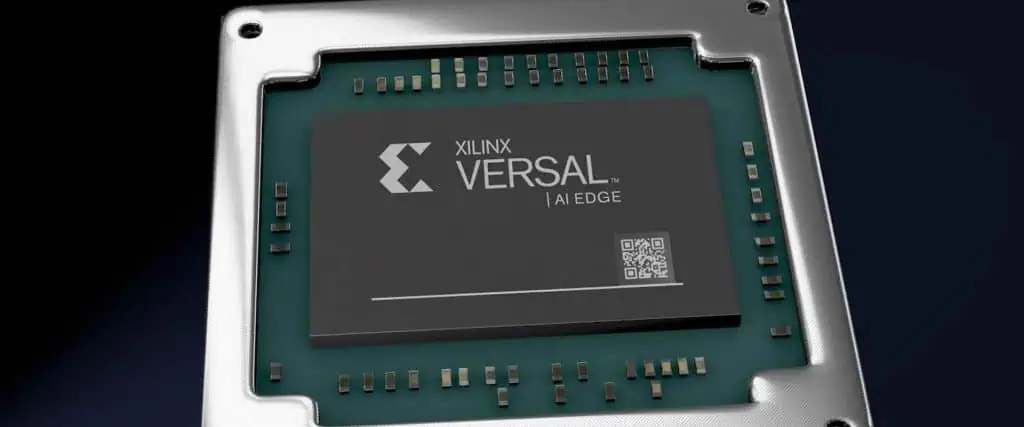
In the ever-evolving landscape of high-performance computing, Xilinx has introduced a game-changing technology: the Versal Adaptive Compute Acceleration Platform (ACAP). This revolutionary architecture combines the best of CPUs, GPUs, and FPGAs into a single, flexible platform. In this comprehensive guide, we’ll delve deep into the Xilinx Versal ACAP, with a particular focus on three key models: the VCK190, VMK180, and VCK5000. We’ll explore their features, performance capabilities, and pricing to help you understand how these cutting-edge devices can accelerate your applications and transform your computing infrastructure.
Understanding Xilinx Versal ACAP
Before we dive into the specific models, it’s crucial to understand what makes the Xilinx Versal ACAP so revolutionary.
What is an ACAP?
An Adaptive Compute Acceleration Platform (ACAP) is a fully software-programmable, heterogeneous compute platform that combines scalar engines, adaptable hardware engines, and intelligent engines with leading-edge memory and interfacing technologies. Unlike traditional FPGAs, ACAPs are designed to be fully programmable and reconfigurable, adapting to the needs of a wide range of applications and workloads.
Key Features of Xilinx Versal ACAP
Scalar Engines: Arm Cortex-A72 and Cortex-R5 processors for general-purpose computing
Adaptable Hardware Engines: Programmable logic for custom hardware acceleration
Intelligent Engines: AI Engines for high-performance AI and DSP workloads
Network-on-Chip (NoC): High-bandwidth, low-latency connectivity between all components
Programmable I/O: Flexible interfaces for various connectivity options
Security Features: Built-in security measures for data protection and secure boot
Benefits of Xilinx Versal ACAP
Flexibility: Adaptable to a wide range of applications and workloads
Performance: High-performance computing for AI, data analytics, and signal processing
Energy Efficiency: Optimized power consumption for demanding applications
Time-to-Market: Faster development cycles with software programmability
Future-Proofing: Adaptable architecture that can evolve with changing requirements
The Xilinx Versal VCK190 is designed specifically for AI and machine learning applications, offering exceptional performance for deep learning inference and training.
VCK190 Key Specifications
AI Engines: 400 AI Engines for high-performance AI workloads
Scalar Engines: Dual-core Arm Cortex-A72 and dual-core Arm Cortex-R5
Adaptable Hardware: 1,968K logic cells
Memory: 34.6Mb on-chip memory and 32GB of DDR4 SDRAM
Connectivity: PCIe Gen4, 100G Ethernet, and various other high-speed interfaces
VCK190 Performance
The VCK190 shines in AI and machine learning applications:
AI Inference: Up to 479 TOPS (INT8) for AI inference workloads
AI Training: Excellent performance for on-device AI training
Signal Processing: High-performance DSP capabilities with 1,968 DSP engines
VCK190 Use Cases
Autonomous Vehicles: Real-time processing of sensor data and decision-making
5G Infrastructure: Baseband processing and beamforming for 5G networks
Healthcare: Medical imaging and analysis, drug discovery acceleration
Financial Services: High-frequency trading and risk analysis
VCK190 Pricing
As of 2023, the Xilinx Versal VCK190 Evaluation Kit is priced at approximately $19,999. However, pricing for production quantities may vary and should be obtained directly from Xilinx or authorized distributors.
The Xilinx Versal VMK180 is designed for applications that require a mix of high-speed digital and analog processing, making it ideal for communications, aerospace, and defense applications.
VMK180 Key Specifications
AI Engines: 256 AI Engines for efficient signal processing
Scalar Engines: Dual-core Arm Cortex-A72 and dual-core Arm Cortex-R5
Adaptable Hardware: 1,312K logic cells
Memory: 38.3Mb on-chip memory and 16GB of DDR4 SDRAM
Connectivity: PCIe Gen4, 100G Ethernet, and high-speed serial transceivers
VMK180 Performance
The VMK180 excels in mixed-signal applications:
Signal Processing: Up to 479 TOPS (INT8) for digital signal processing
Analog Processing: High-performance ADCs and DACs for direct RF sampling
Customizable Logic: Flexible adaptable hardware for custom accelerators
VMK180 Use Cases
Electronic Warfare: Real-time signal intelligence and jamming systems
Software-Defined Radio: Flexible, multi-protocol radio systems
Radar Systems: Advanced radar processing and beamforming
Test and Measurement: High-performance instrumentation and data acquisition
VMK180 Pricing
The Xilinx Versal VMK180 Evaluation Kit is priced similarly to the VCK190, at around $19,999. Again, production pricing may vary and should be obtained directly from Xilinx.
The Xilinx Versal VCK5000 is a veritable powerhouse designed for data center acceleration, offering unprecedented performance for a wide range of compute-intensive applications.
VCK5000 Key Specifications
AI Engines: 400 AI Engines for massive parallel processing
Scalar Engines: Quad-core Arm Cortex-A72 and dual-core Arm Cortex-R5
Adaptable Hardware: 1,968K logic cells
Memory: 34.6Mb on-chip memory and 32GB of HBM2e
Connectivity: PCIe Gen4 x16, 100G Ethernet, and CCIX
VCK5000 Performance
The VCK5000 sets new standards for compute acceleration:
AI Performance: Up to 479 TOPS (INT8) and 119 TFLOPS (FP16)
Memory Bandwidth: 820 GB/s with HBM2e memory
Network Performance: 100Gbps network connectivity
VCK5000 Use Cases
Data Center Acceleration: Offloading compute-intensive tasks from CPUs
AI/ML Acceleration: High-performance training and inference for large models
Database Acceleration: In-memory database processing and analytics
Video Processing: Real-time video transcoding and analytics at scale
VCK5000 Pricing
The Xilinx Versal VCK5000 is a high-end data center product, and its pricing reflects its premium positioning. While exact pricing is not publicly available and may vary based on volume and specific configurations, it is estimated to be in the range of 30,000to30,000to50,000 per unit. For accurate pricing, interested parties should contact Xilinx directly.
Performance Comparison: VCK190 vs VMK180 vs VCK5000
To better understand how these Xilinx Versal ACAP models compare, let’s look at a side-by-side comparison of their key performance metrics:
Feature
VCK190
VMK180
VCK5000
AI Engines
400
256
400
Logic Cells
1,968K
1,312K
1,968K
AI Performance (INT8)
479 TOPS
479 TOPS
479 TOPS
Memory
32GB DDR4
16GB DDR4
32GB HBM2e
Memory Bandwidth
~40 GB/s
~40 GB/s
820 GB/s
Primary Use Case
AI/ML
Mixed-Signal
Data Center
Key Takeaways from the Comparison
AI Performance: All three models offer impressive AI performance, with the VCK190 and VCK5000 leading in terms of AI Engine count.
Memory: The VCK5000 stands out with its high-bandwidth HBM2e memory, making it ideal for data-intensive applications.
Flexibility: The VMK180 offers a balance of digital and analog capabilities, making it versatile for mixed-signal applications.
Scalability: The VCK5000’s data center focus makes it highly scalable for large-scale deployments.
Pricing Considerations and ROI
When considering the pricing of Xilinx Versal ACAP devices, it’s important to look beyond the initial cost and consider the total cost of ownership (TCO) and return on investment (ROI).
Factors Affecting TCO and ROI
Performance Gains: The significant performance improvements can lead to reduced infrastructure needs and lower operational costs.
Power Efficiency: Versal ACAPs offer better performance per watt compared to traditional solutions, potentially lowering energy costs.
Flexibility and Future-Proofing: The adaptable nature of ACAPs means they can be repurposed for different workloads, extending their useful life.
Development Time: Software programmability can lead to faster development cycles and quicker time-to-market.
Consolidation: ACAPs can replace multiple discrete components, simplifying system design and reducing overall costs.
Evaluating ROI for Different Applications
AI/ML Projects: Consider the cost savings from accelerated training times and improved inference performance.
5G Infrastructure: Evaluate the benefits of flexible, software-defined networking capabilities in reducing upgrade costs.
Data Center Acceleration: Calculate the potential savings from improved server utilization and reduced power consumption.
Edge Computing: Assess the value of high-performance, low-latency processing at the edge in reducing data transfer costs and improving response times.
Development Tools and Ecosystem
To fully leverage the power of Xilinx Versal ACAPs, a robust set of development tools and a supportive ecosystem are crucial.
Vitis™ Unified Software Platform
Xilinx provides the Vitis™ unified software platform, which includes:
Vitis AI: Tools for AI model development and optimization
Vitis Accelerated Libraries: Pre-optimized libraries for common functions
Vitis Video: Video processing acceleration tools
Vitis Data Analytics: Tools for accelerating data analytics workloads
Vivado Design Suite
For hardware designers, the Vivado Design Suite offers:
High-Level Synthesis: C/C++ to hardware description language conversion
IP Integrator: Graphical design environment for IP-based design
Simulation and Debugging Tools: Comprehensive tools for design verification
Third-Party Tools and Support
The Xilinx ecosystem includes support for popular frameworks and tools:
TensorFlow and PyTorch: Integration with popular AI frameworks
MATLAB and Simulink: Support for model-based design
To illustrate the impact of Xilinx Versal ACAPs, let’s look at some real-world applications and success stories:
Case Study 1: 5G Infrastructure Acceleration
A major telecommunications company implemented the Xilinx Versal VMK180 in their 5G base stations, resulting in:
40% reduction in power consumption
3x improvement in spectral efficiency
Flexible support for multiple 5G standards through software updates
Case Study 2: Autonomous Vehicle Sensor Fusion
An automotive AI company used the Xilinx Versal VCK190 for real-time sensor fusion in their autonomous driving platform, achieving:
5x improvement in object detection accuracy
70% reduction in latency for critical decision-making
Ability to process data from multiple sensors (LiDAR, radar, cameras) in real-time
Case Study 3: Financial Risk Modeling
A leading financial institution deployed the Xilinx Versal VCK5000 in their data center for risk modeling and analysis, resulting in:
10x acceleration of Monte Carlo simulations
80% reduction in time-to-insight for complex risk scenarios
Significant cost savings from reduced CPU usage and energy consumption
Future of Xilinx Versal ACAP
As we look to the future, the Xilinx Versal ACAP platform is poised for continued growth and innovation:
Emerging Applications
6G Research: As 6G technology begins to take shape, Versal ACAPs are well-positioned to support the development of next-generation wireless systems.
Quantum Computing Integration: ACAPs could play a crucial role in interfacing classical systems with quantum computers.
Advanced Robotics: The combination of AI and adaptable hardware makes Versal ideal for next-generation robotics applications.
Technology Roadmap
While specific details of future Versal generations are not public, we can expect:
Increased AI Engine Density: More AI Engines per chip for even higher AI performance.
Advanced Process Nodes: Migration to more advanced semiconductor process nodes for improved power efficiency.
Enhanced Memory Integration: Potential for even higher bandwidth memory solutions.
Expanded Ecosystem: Continued growth of the software and IP ecosystem to support a wider range of applications.
Conclusion: The Transformative Power of Xilinx Versal ACAP
The Xilinx Versal ACAP represents a significant leap forward in adaptive computing technology. With its unique combination of scalar engines, adaptable hardware, and AI engines, Versal offers unprecedented flexibility and performance for a wide range of applications.
The VCK190, VMK180, and VCK5000 models each target specific application areas:
VCK190: Ideal for AI-focused applications requiring high inference and training performance.
VMK180: Perfect for mixed-signal applications in communications, aerospace, and defense.
VCK5000: A powerhouse for data center acceleration and high-performance computing.
While the initial investment in Versal technology may seem significant, the potential returns in terms of performance gains, energy efficiency, and flexibility make it an attractive option for organizations looking to stay at the forefront of technology.
As we move into an era of increasingly complex and data-intensive applications, the adaptable nature of Xilinx Versal ACAPs positions them as a key enabling technology for the next generation of computing innovations. Whether you’re developing autonomous systems, building 5G infrastructure, or pushing the boundaries of AI and data analytics, Xilinx Versal ACAP offers the performance, flexibility, and efficiency to turn your most ambitious ideas into reality.
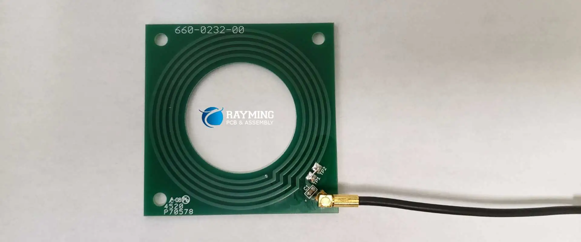
Printed circuit boards (PCBs), used in various electronic devices, must include filled vias. These vias, which are effectively tiny holes punched into the PCB, connect the various layers of the board. Via holes filled and sealed with conductive or non-conductive material or copper plating are known as filled vias.
Types of Filled Vias
Filled vias come in various varieties, each with special benefits and drawbacks. They consist of the following:
Conventional Filled Vias
The most typical kind of filled vias is conventional vias. This sort of via involves drilling a tiny hole through the PCB and filling it with copper using an electroplating technique. The copper adds to the hole’s walls; we remove any extra to provide a level surface. Traditional filled vias are dependable and suitable for usage in most PCB applications. They can be produced in large quantities and are also reasonably priced.
Through-Hole Vias
All layers of the PCB, from the top to the lowest layer, are connected by through-hole vias. A hole is bored through the entire board to create a through-hole via, which is subsequently filled with copper. When a significant quantity of current must transfer across various board layers, through-hole vias are helpful. They are also more dependable than other through kinds since mechanical stress is less likely to cause them to disconnect.
Blind vias run from the PCB’s top layer to one or more of its interior layers but stop short of going through the board. Instead, a hole is drilled through the top layer and into the inner layer to create a blind via, filled with copper. Blind vias come in handy for applications without room to drill a hole through the board. Because they require less drilling and plating than through-hole vias, they are also less expensive.
Buried Vias
Vias connecting two or more of the PCB’s inner layers but not extending to the top or bottom layers are known as buried vias. A hole is drilled through two inner layers to create a buried via filled with copper. Hidden vias come in handy for applications where numerous layers of the PCB and drilling through the entire board would damage the other layers. Because they require less drilling and plating than through-hole vias, they are also less expensive.
Microvias
Microvias are extremely small vias with a 0.15mm or less diameter. They are helpful when there is insufficient room for conventional or blind vias. We can produce microvias using a laser drilling procedure that makes a tiny hole in the circuit board. This hole is subsequently filled with copper using an electroless plating procedure. Since they need more precise processing and equipment, microvias are more expensive than other via kinds.
Stacked Microvias
Similar to regular microvias, stacked microvias help to connect different PCB layers. Drilling numerous tiny holes in the board and filling them with copper results in stacked microvias. Applications requiring a high connection density but a limited area can benefit from stacked microvias.
Benefits of Filled Vias
Vias are critical in linking the various layers of printed circuit boards (PCBs). Through-hole or surface-mount vias are essential for maintaining the connectivity of the various PCB components.
Improved Reliability:
The reliability of a PCB improves by filled vias, which is one of its most important advantages. Filled vias can lower the possibility of failure because of temperature fluctuations, vibration, and moisture intrusion. This is because filled vias contribute to a stronger, more reliable connection between the various layers of a PCB. In addition, the board is less likely to crack or break thanks to the filler substance used in the vias, which serves to lessen stress.
Enhanced Thermal Performance:
Furthermore, filled vias improve a PCB’s thermal performance. This is due to the through-filling material’s ability to provide more effective heat transfer, which lowers the board’s operating temperature. This can be crucial for high-performance systems that produce much heat, such as those in the telecommunications, aerospace, and defense sectors.
Improved Signal Integrity:
Another significant benefit is the capacity of filled vias to improve the signal integrity of a PCB. This is because the filler material used in the vias aids in reducing signal losses and noise, both of which can adversely affect the board’s performance. Using filled vias to connect the various layers of a printed circuit board can increase signal transmission accuracy and interference-free operation (PCB).
Better Electrical Performance:
Filling vias with conductive materials such as copper can increase their capacity to carry current from one layer to another, which enhances electrical performance. Copper-filled micro-vias can also improve thermal and electrical conductivity, reduce EMI, and allow for high routing density on the PCB. However, filling vias with non-conductive materials such as epoxy can also somewhat improve electrical conductivity. Additionally, thermal vias can transfer heat from one layer to another on the same board, improving thermal management and overall electrical performance.
Increased Density:
A PCB’s density can also increase by using filled vias. This is because they occupy less space on the board than conventional through-hole vias, allowing for the placement of more components. This can be especially crucial for designs that need a high level of functionality in a tiny form factor.
Cost Savings:
Although filled vias can cost more than conventional through-hole vias, they may save you money over time. This is because filled vias can contribute to a PCB’s overall size reduction, resulting in material and production cost savings. Moreover, using filled vias can lessen the chance of failure, saving money by preventing warranty claims and product recalls.
Easier Assembly:
Furthermore, filled vias can simplify the PCB assembly process. This is so that the components on the board have more support from the filler material utilized in the vias, which will reduce the likelihood of movement or displacement during assembly. Moreover, filled vias can aid in lowering the possibility that the board would damage during assembly, which can result in cost savings and quicker production.
Printed circuit board (PCB) manufacture uses the via-filling technique to fill via holes with conductive or non-conductive material. Via holes are tiny holes punched in the PCB that link its various layers together. Via filling is crucial in manufacturing PCBs since it ensures the board will function correctly and dependably.
The following steps are commonly helpful in the filling process:
Preparing the board:
The board must be clean before the through-filling procedure starts. It is crucial to ensure the board is clean and clear of any contaminants because any dirt, debris, or residue on the board can hinder the adhesion of the filling material.
Drilling the holes:
Drilling the via holes into the board is the next step. A computer-controlled drilling machine is often helpful because it can create precise holes at the right depths and places. The board’s characteristics and the components that will mount on it determine the size of the holes.
Cleaning the holes:
Once you drill the holes, you must clean them to eliminate any dust or debris gathered during the drilling procedure. You can remove loose debris from the holes using a vacuum cleaner or a high-pressure air pistol, which are both commonly helpful.
Applying the filling material:
The filling material can be essential after cleaning the holes. Depending on the board’s needs, this substance may be either conductive or non-conductive. Non-conductive fillers often consist ofsubstances like epoxy resin, whereas conductive fillers frequently comprise metals like copper or silver.
Curing the material:
The filler substance needs to curing or hardening after application. We can accomplish this using heat, UV light, or other curing techniques, depending on the material utilized. A stable and dependable connection between the various layers of the board becomes possible by the material’s ability to harden and bond with the walls via holes during the curing process.
Finishing the board:
We can apply a final layer of protective coating or solder mask to the board once the filler substance has dried and hardened. This layer offers a smooth and homogeneous surface for mounting components and aids in shielding the board from deterioration, corrosion, and other forms of wear and tear.
Depending on the needs of the board and the manufacturer’s capabilities, various through-filling techniques are ideal. Typical techniques include:
Plated through-hole (PTH) filling: We must electroplate and deposit metal via holes. The method involves submerging the board in an electrolyte solution and running an electrical current through the metal, commonly copper. We make a strong and conductive link between the various layers of the board when the copper ions bond with the walls of the via holes due to the current.
Non-conductive epoxy filling: This technique uses epoxy resin to fill the via holes, which hardens and connects with the hole walls. Since epoxy glue is non-conductive, it does not affect the board’s electrical characteristics. Normally, non-critical applications where conductivity is unimportant utilize this strategy.
Conductive paste filling: Conductive paste comprises metal shavings, and pour a binder into the via holes. We usually apply the paste by screen printing, and once it has dried, it hardens and adheres to the walls of the via holes. This technology is often helpful for low-density boards when the cost is an issue.
Conclusion
Electronic devices cannot function without printed circuit boards (PCBs); vias are crucial to PCB design. A via is a tiny hole drilled through two or more adjacent copper layers on a printed circuit board (PCB) and then plated with copper to form an electrical connection between the copper layers. Vias of various forms, including through-hole vias, microvias, and via-in-pad designs, are helpful in PCBs.
A PCB manufacturing process known as via filling involves filling through a hole with a conductive or non-conductive substance, such as epoxy, to enhance signal integrity, heat management, and reliability. With better thermal conductivity and dissipation, copper-plated shut-filled vias are more recent and sophisticated via filling. According to the individual needs of their PCB design, PCB designers must consider the via type and via the filling procedure to utilize.
Field-programmable gate array is FPGA. It is a kind of integrated circuit (IC) that, after production, may be customized and programmed by the user. FPGAs can be reprogrammed and tailored to multiple applications or functions, unlike application-specific integrated circuits (ASICs), created for a particular purpose.
We can build custom digital circuits using programmable logic blocks, configurable input/output blocks, and programmable routing resources in FPGAs. These gadgets are frequently helpful in computer networking, video and image processing, aerospace, and defense.
FPGAs have several benefits over conventional ASICs, including a quicker time to market, less expensive development, and more flexibility. Additionally, they eliminate the need for a costly and time-consuming professional ASIC design team, enabling designers to integrate unique logic functions.
How it works
Input/output blocks (IOBs), programmable routing resources, and configurable logic blocks (CLBs) comprise most FPGA components. These components are all connected via a programmable interconnect structure. When coupled, any bespoke digital logic function can be implemented using this set of configurable blocks and resources.
Configuration and operation are the two primary processes in the fundamental operation of an FPGA.
Configuration: The FPGA must be set up with the desired logic architecture because it was originally empty. Usually, a hardware description language (HDL) like VHDL or Verilog is ideal. Then, a configuration bitstream created from the HDL code synthesizes, compiled, and placed into the FPGA’s non-volatile configuration memory.
Operation: Once configured, the FPGA can be helpful like any other digital circuit. The user-defined logic functions in the CLBs process the input signals once they route through the IOBs and programmable interface to those devices. The connection and IOBs then help to return output signals to the external devices.
Compared to conventional hardware designs, FPGAs have several benefits, including:
Flexibility: FPGAs are incredibly adaptable and can program it for various jobs. As a result, fewer hardware designs are necessary because a single FPGA can be helpful for several applications.
Price: Generally, FPGAs are less expensive than conventional hardware designs, especially for low to medium manufacturing volumes. After all, FPGAs can be programmed and reprogrammed to carry out various jobs.
Time-to-Market: Compared to conventional hardware designs, FPGAs can be programmed and tested significantly more quickly. This means that new items can be introduced to the market more quickly, which is crucial in sectors like consumer electronics.
Performance: For applications requiring sophisticated logic functions, FPGAs can perform better than conventional hardware architectures. This is due to the flexibility of FPGAs, which may be modified as necessary and optimized to do particular jobs.
Power usage: FPGAs can use less power than conventional hardware layouts. This is so that FPGAs can carry out specified jobs with the least amount of resource waste possible.
However, there are disadvantages to using FPGAs, including:
Complexity: Compared to conventional hardware designs, FPGAs might be more challenging to design and program. FPGAs need expertise in hardware description languages and specialized programming and testing tools.
Price: FPGAs can be more expensive for high-volume production, despite being less expensive than conventional hardware designs for small to medium production levels. This is due to the unique manufacturing procedures needed for FPGAs.
Limited Resources: FPGAs have only a certain amount of CLBs, IOBs, and routing resources. This indicates that larger and more intricate designs would need additional FPGAs, which could raise the cost.
Latency: Compared to conventional hardware designs, FPGAs may contribute more latency. Setting up and programming FPGAs before using them takes more time.
Lattice FPGA
Lattice Field-Programmable Gate Arrays (FPGAs) are a class of reconfigurable programmable logic devices we can set up for various tasks. For example, several industries use telecommunications, automotive, industrial control, medical, and the military.
Lattice FPGAs are unique in their low power consumption, which makes them perfect for situations where power consumption is crucial. They are also appropriate for usage in applications with limited space because of their tiny form factor.
Hardware description languages (HDLs), such as Verilog and VHDL, can program Lattice FPGAs. Lattice FPGA designs are created, simulated, and implemented using the Lattice Diamond software suite. The software package consists of a GUI for entering designs, a compiler for turning designs into netlists, and a place-and-route tool for placing designs on FPGAs.
The built-in intellectual property (IP) blocks in Lattice FPGAs include memory controllers, high-speed transceivers, and DSP blocks, among others. These IP-building pieces can be incorporate into a design to simplify production
Several families of lattice FPGAs exist, each with distinctive features and abilities. The ECP5, MachXO3, and CrossLink-NX families of Lattice FPGAs are a few well-liked families.
A global routing network links the programmable logic blocks (PLBs) in a hierarchy found in lattice FPGAs (GRN). Each PLB comprises a flip-flop and a customizable logic block (CLB) arranged in rows and columns. We implement the Boolean logic functions of the design by the CLB, which is the fundamental component of the FPGA. The flip-flop helps synchronize and store data.
Lookup table and multiplexer
A lookup table (LUT) and multiplexer comprise the CLB (MUX). The truth table of a Boolean function sits in the LUT, a programmable memory. We choose the output of the LUT or the input from the next CLB using the MUX. Carry chains are another feature of the CLBs for quick addition and subtraction operations.
GRN
Signals must be routed between the PLBs by the GRN. The inputs and outputs of the CLBs connect by a system of horizontal and vertical wires known as the GRN. Moreover, the GRN has programmable switches that the designer can use to link the PLBs in any pattern they like.
Dedicated resources
Furthermore, we can implement memory and arithmetic operations using specialized resources in lattice FPGAs. Specifically, designed blocks for implementing RAM, ROM, and DSP functions are among these resources. Furthermore, arranging the RAM blocks as single-port or dual-port memory is possible. Moreover, we can set up the ROM blocks. Finally, the implementation of arithmetic operations, including addition, subtraction, multiplication, and division, is optimized for the DSP blocks.
Clock management resources
Furthermore, clock management resources are provided by lattice FPGAs, enabling the designer to produce and distribute clocks throughout the system. These tools include delay-locked loops (DLLs) and programmable phase-locked loops (PLLs), which may produce clocks with various frequencies and phases. To ensure that the clock signals reach various components of the design simultaneously, the PLLs and DLLs can also be helpful for clock skew management.
High-speed serial interfaces
Moreover, Lattice FPGAs have resources set aside for implementing high-speed serial interfaces like USB, Gigabit Ethernet, and PCI Express. In addition, physical layer (PHY) circuits, serializers, and deserializes are resources that implement the interface’s electrical and low-level signaling requirements.
Configuration memory
Lattice FPGAs additionally have a configuration memory that houses configuration and design data. Many techniques can program the configuration memory, including JTAG, SPI, and a separate configuration bus. In addition, we can modify a piece of the FPGA without affecting the remainder of the design thanks to a configuration memory feature that enables partial reconfiguration of the FPGA.
Power management resources
Lattice FPGAs also provide several power management capabilities that the designer can use to lower the design’s power usage. These capabilities include low-power modes, which allow the FPGA to be put into a low-power state when not in use, and dynamic power management, which enables unneeded design components to turn off to save power consumption.
Programming Lattice FPGA
FPGAs are programmable devices to carry out particular functions or create digital circuits. FPGAs comprise a grid of programmable logic cells coupled with programmable routing resources. One of the top FPGA producers, Lattice Semiconductor, provides a broad selection of devices for various purposes.
Lattice FPGA development environments needs setting up in several different ways. This is an overview:
Lattice Diamond software installation: Most FPGA development using Lattice devices uses this software. Follow the installation wizard after downloading it from the Lattice Semiconductor website.
Setup the cables for Lattice programming: You might need to add particular programming connections depending on your kind of Lattice FPGA. The Lattice Semiconductor website has the drivers and installation instructions.
Get your FPGA board ready: Use USB or another compatible interface to connect your FPGA board to your PC. To ensure it is powered on and connected correctly, adhere to the manufacturer’s instructions.
Make a new undertaking: Open a new project in the Lattice Diamond software. Choose your FPGA device from the list of compatible devices and adjust the project settings as necessary.
Put your VHDL or Verilog code here: Either write your code in Verilog or VHDL using the Lattice Diamond program. These are the two main programming languages for FPGAs.
Make a model of your design: Before synthesizing your design for the FPGA, test it using Lattice Diamond’s simulation tool.
Create a binary file that can be put onto the FPGA by synthesizing your design using the Lattice Diamond synthesis tool.
Configure your FPGA: The binary file produced in the preceding step should be used to program the FPGA using the Lattice programming tool included in Lattice Diamond.
After completing these procedures, your Lattice FPGA development environment should be completely operational.
Creating a new project
Creating a new project in Lattice Diamond is the initial step in programming a Lattice FPGA. A project, a collection of design files and configuration information, defines an FPGA design. Go to file ~, then New ~, then Project in Lattice Diamond, and choose the device family and type corresponding to your intended FPGA board to start a new project. Next, select the project’s name and location before clicking OK.
Adding design files to the project
The project needs to have design files added once we create it. This is because the source code for the FPGA design is in design files written in a Hardware Description Language (HDL) like Verilog or VHDL. By selecting Add Sources from the context menu when you right-click the project name in the Project Navigator in Lattice Diamond, we can add design files to the project.
Any text editor or integrated development environment (IDE), such as Xilinx Vivado or Quartus Prime, can be used to create design files. However, the behavior and functionality of an FPGA design depend on a top-level module that instantiates other modules or components.
Synthesizing the design
We must combine the design after adding the design files to the project. A netlist, an illustration of the FPGA architecture in terms of logic gates and flip-flops, is created through synthesis, which involves translating the HDL code into a netlist. The Lattice Synthesis Engine (LSE), a part of Lattice Diamond, is used for synthesis.
Choose Synthesize Design from the Process menu in Lattice Diamond to synthesize the design. The LSE tool will then start and analyze the HDL code to produce a netlist. Depending on the needs of the design, the LSE tool offers a variety of synthesis options, including optimization level, technology mapping, and clock domain analysis.
Implementing the design
We must put the design into practice when it synthesizes. Implementing the requested functionality involves mapping the netlist onto the FPGA architecture, configuring the programmable logic cells, and allocating resources. The Lattice Diamond Place-and-Route (P&R) tool is helpful for implementation, and it creates a bitstream file by mapping the netlist onto the FPGA design.
Choose Implement Design in Lattice Diamond’s Process menu to implement the design. Then, the Place-and-Route (P&R) tool will launch, mapping the netlist onto the FPGA architecture and creating a bitstream file.
The P&R tool performs several operations, such as placement, routing, and time analysis. The physical location of each logic cell on the FPGA depends on the placement. Routing entails configuring the interconnect resources to connect the logic cells following the netlist. Finally, by performing timing analysis, you can ensure the design complies with the timing specifications in the HDL code.
It’s crucial to set up the implementation settings correctly based on the design specifications during implementation. This entails picking the appropriate FPGA family and device, establishing the I/O restrictions, and defining the timing and power parameters.
Once the implementation is complete, the P&R tool creates a bitstream file with the FPGA configuration information. Then, the Diamond Programmer tool can download the bitstream file to the FPGA.
Once the bitstream file is ready, you can download it to the target FPGA board to begin programming the FPGA. The Diamond Programmer tool, which supports various programming modes, including JTAG, SPI, and flash programming, can accomplish this.
Connect the target FPGA board to the computer via a USB cable, then start the Diamond Programmer tool to program the FPGA. First, choose the programming mode, then select the programming parameters to match the target FPGA board. The bitstream file will then be downloaded to the FPGA when you pick it and click program.
After programming, the FPGA will perform the desired functionality provided in the HDL code. We may rapidly prototype and develop FPGA designs since we can reprogram the FPGA as often as necessary.
Debugging the design
FPGA design must include debugging since it enables us to find and correct design flaws. Lattice Diamond offers several tools for debugging FPGA designs, including simulation, timing analysis, and waveform visualization.
Simulation entails simulating the HDL code with a simulator tool, such as ModelSim or Aldec Active-HDL. Before programming the FPGA, we can use simulation to evaluate the design’s functionality and find any problems or errors in the HDL code.
Timing analysis entails examining the design’s timing performance to ensure it complies with the timing specifications stated in the HDL code. Lattice Diamond offers a timing analyzer tool that enables us to examine the design’s timing performance and spot any timing inaccuracies.
Waveform watching entails utilizing a waveform viewer tool, such as Lattice Reveal, to observe the signals and data flow in the design. By inspecting the waveform, we can see how the design behaves and spot any problems or errors in the HDL code.
Application
Industrial application of Lattice FPGA
Lattice FPGAs are helpful in several industrial applications in numerous sectors. For example, lattice FPGAs are frequently essential in the following industrial applications:
Industrial Automation:
Lattice FPGAs are used in industrial automation to operate robots, monitor, and manage production processes, and set up machine vision systems, among other things. FPGAs are perfect for industrial automation applications with high-speed data processing and minimal latency since they provide real-time processing capabilities.
Communications:
To accomplish high-speed data transport, signal processing, and protocol conversion, communication systems utilize lattice FPGAs. Furthermore, FPGAs are employed in cable, optical, and wireless communication systems to increase performance and decrease delay.
Test and Measurement:
In test and measurement devices like oscilloscopes, signal analyzers, and network analyzers, lattice FPGAs are suitable. FPGAs are perfect for test and measurement applications that call for high precision and low latency because they can process data at high speeds and in real time.
Energy:
Energy applications include the monitoring and control of energy distribution networks, the implementation of energy management systems, and the control of power-producing systems. FPGAs are perfect for building energy-efficient systems since they have a high performance to low-power consumption ratio.
Medical:
Lattice FPGAs are helpful in medical applications to interpret medical imaging data, monitor vital signs, and control medical equipment. FPGAs are perfect for medical applications requiring real-time processing and low energy usage due to their high performance and low power consumption.
Aerospace and Defense:
Lattice FPGAs are helpful in aerospace and defense applications for various functions, including managing radar, missile guidance, and avionics systems. FPGAs are perfect for aerospace and defense applications that demand robustness and endurance in severe environments because of their high dependability and radiation tolerance.
Automotive application of Lattice FPGA
There are numerous uses for lattice FPGAs in the automobile sector. For example, lattice FPGAs are frequently essential in the following automotive applications:
Advanced Driver Assistance Systems (ADAS):
For purposes like object identification, lane departure warning, and collision avoidance, lattice FPGAs are helpful in ADAS. In addition, FPGAs are perfect for ADAS applications that need high-speed data processing and minimal latency since they have real-time processing capabilities.
Engine Management Systems:
Lattice FPGAs are helpful in engine management systems to regulate the timing of the ignition, fuel injection, and other aspects of the engine. FPGAs are perfect for building intricate engine control systems because of their high performance and low power consumption.
Lattice FPGAs are helpful in in-car entertainment systems to perform audio processing, video decoding, and user interface control. FPGAs are the best choice for incorporating cutting-edge infotainment features in contemporary vehicles because they combine great performance and low power consumption.
Head-Up Displays (HUDs):
HUDs use lattice FPGAs to project critical driving data onto the windscreen, such as speed, directions, and safety alerts. FPGAs are perfect for implementing advanced HUD features because they provide real-time processing and high-resolution graphics capabilities.
Tire Pressure Monitoring Systems (TPMS):
To monitor tire pressure and identify probable tire failures, TPMS uses lattice FPGAs. FPGAs are perfect for constructing TPMS systems that constantly run without depleting the car’s battery because they have high data processing speeds and little power consumption.
Adaptive Lighting Systems:
Adaptive lighting systems use lattice FPGAs to change the headlights according to speed, weather, and kind of road. FPGAs are perfect for building sophisticated lighting control systems that increase driver safety and visibility since they have real-time processing capabilities.
Vehicle-to-Vehicle (V2V) and Vehicle-to-Infrastructure (V2I) Communications:
Vehicle-to-vehicle and vehicle-to-infrastructure communication are possible using lattice FPGAs in V2V and V2I communication systems. In addition, FPGAs are perfect for building real-time communication systems that can increase traffic safety and efficiency because they provide high-speed data processing and low latency.
Consumer electronics application
Lattice FPGAs’ excellent performance, low power consumption, and flexibility make them useful in various consumer electronics applications. For example, lattice FPGAs are frequently helpful in the following consumer electronics applications:
Mobile Devices:
Mobile devices use lattice FPGAs to process audio and video, manage batteries, and process sensor data. FPGAs are perfect for incorporating sophisticated features in mobile devices while preserving battery life because they combine great performance with low power consumption.
Gaming:
For activities like audio and video processing, user interface control, and picture identification in gaming applications, lattice FPGAs are helpful. FPGAs are perfect for integrating sophisticated gaming features and enhancing user experience since they provide real-time and high-speed data processing capabilities.
Virtual and Augmented Reality:
In virtual and augmented reality systems, lattice FPGAs are helpful for operations like image and video processing, sensor data processing, and user interface control. In addition, FPGAs are perfect for integrating real-time virtual and augmented reality features because of their high performance and low latency.
Audio and Video Processing:
Applications for audio and video processing, including soundbars, smart speakers, and video streaming devices, utilize lattice FPGAs. FPGAs are perfect for integrating advanced audio and video processing features while reducing energy usage since they have excellent performance capabilities and low power consumption.
Robotics and Drones:
Robotics and drone applications use lattice FPGAs for sensor data processing, navigation, and control. FPGAs are perfect for creating complicated robotic and drone systems since they have tremendous performance capabilities and consume less power.
Home Automation:
Applications for home automation use lattice FPGAs to interpret sensor data, manage connected devices, and develop voice assistants. FPGAs are the best choice for building power-efficient home automation systems because of their excellent performance capabilities and low power consumption.
Wearable Devices:
In wearable technology, lattice FPGAs are suitable for battery management, user interface control, and sensor data processing. In addition, FPGAs are perfect for building wearable technology that can run continuously for a long time because they have excellent performance capabilities and use little power.
Mister FPGA’s hardware and software project aims to use an FPGA chip to simulate the operation of vintage video game consoles, PCs, and arcade machines.
The hardware platform offered by the project consists of an FPGA board called the “Mister” board and several add-on boards that support various systems. The FPGA may then execute software as if it were the original hardware by having users load “cores” of software that mimic the hardware of a particular console or computer.
Mister FPGA accurately simulates the original hardware at a low level. As a result, it makes it a very accurate way to operate vintage computing systems and play classic games. The FPGA architecture also makes it possible to design new cores. As a result, enthusiasts can add to the system to support different devices. As a result, the project has a sizable fan base among retro gaming fans and has emerged as a preferred method of enjoying vintage video games and computing devices.
Why Mister FPGA is a popular alternative to classic consoles
Mister FPGA PCB Board
Mister FPGA is a well-liked substitute for vintage consoles for several reasons:
Accuracy: Mister FPGA accurately reproduces the hardware of vintage consoles, PCs, and arcade games. This results in an accurate and true experience because software operating on the Mister platform behaves like running on the original hardware.
Versatility: The Mister FPGA platform supports various devices, including arcade machines, retro computers like the Amiga and Atari ST, and old consoles like the NES and Sega Genesis. Users can have a single device that can simulate a variety of systems thanks to its adaptability.
Preservation: It’s getting harder and harder to find vintage video games, computers, and arcade devices because manufacturers are no longer manufacturing them. Users that use Mister FPGA can use old software and play games without the requirement for the original hardware, protecting these systems for future generations.
Users can highly customize Mister FPGA, who can add their own “cores” to the system that simulate various hardware systems. But, of course, this implies that we can enhance the platform to enable additional features and systems.
Comparison to software emulation and hardware clones
Compared to Mister FPGA, two other standard methods for playing old games and using historical computing systems are software emulation and hardware clones, each of which has pros and cons.
Software emulation
Emulating software is the technique of running software on a current device. It mimics the hardware of a retro console or computer. Without the need for original hardware, users can play retro games and use vintage software by downloading and installing emulator software. One of the key benefits of software emulation is that we can install it on any contemporary device, which is frequently free or inexpensive.
However, software emulation might have accuracy problems because emulators might not accurately reproduce the original hardware. As a result, it can cause hiccups or inconsistencies in the functionality or gameplay. Furthermore, software emulation demands a lot of computing power. Additionally, the host device’s performance can affect how well the emulation performs.
Hardware clones
On the other hand, hardware clones are actual objects created to use contemporary parts to mimic the functionality of vintage consoles or computers. As a result, software emulation generally lacks the authenticity of hardware clones, frequently made to appear and feel like the original gear. Furthermore, hardware clones can frequently offer a more reliable and accurate experience than emulation because they are not dependent on the host device’s processing capability. Clones of the original hardware, however, might be pricey and may not be able to accurately recreate it, which could cause compatibility problems or flaws in the gameplay or functioning.
Mister FPGA has several benefits over hardware clones and software emulation. First, because Mister FPGA closely mimics the original hardware at a basic level, it offers a very accurate approach to operating vintage computing systems and playing classic games. This results in an accurate and true experience because software operating on the Mister platform behaves like running on the original hardware. Moreover, Mister FPGA offers customers a flexible platform that can imitate a variety of devices, including a wide range of systems, from ancient PCs to classic consoles.
Second, Mister FPGA offers an incredibly configurable platform. Users can add their own “cores” to the system, which simulate various hardware systems. This implies that the platform can handle new systems and features, offering a flexible platform for old-school video games and computer fans.
Moreover, because Mister FPGA is a single device that can imitate numerous distinct systems, it offers a very portable platform. This allows customers to take the Mister FPGA wherever they go and offers a practical method to play retro games and use old computing platforms.
Setting up Mister FPGA on a computer can be challenging, but we can do it in several simple steps. The following is a general setup guide for Mister FPGA on a computer:
Step 1: Choose Your Hardware
Selecting the hardware for your Mister FPGA setup is the first step. The DE-10 Nano and the IO Board, the suggested hardware elements for Mister FPGA, are just two choices. Once you have the necessary hardware, you must assemble the parts and ensure they are linked correctly.
Step 2: Download the Required Software
We must download the essential software for Mister FPGA next. Both the SD card image, which contains the operating system and software necessary to run the Mister FPGA system, and the Mister FPGA core, which is the software that emulates the hardware of the console or computer you want to use, are included in this.
Step 3: Write the SD Card Image
After downloading, you must use software like Etcher or Win32DiskImager to write the SD card image to an SD card. The SD card will include the software and operating system needed to run Mister FPGA.
Step 4: Configure the FPGA Core
The FPGA core must then run to simulate the hardware of the desired console or computer. To accomplish this, you must download the core file and copy it to the SD card. Next, we must configure the core parameters by editing the INI file on the SD card. The configuration options for the core stay in a text file called an INI file.
Step 5: Connect to a Monitor or TV
You can use an HDMI connection to link your Mister FPGA setup to a monitor or TV once you’ve written the SD card image and set up the FPGA core. A USBkeyboard and mouse can also be helpful with the configuration of input devices.
Step 6: Power Up and Test
Your Mister FPGA system can now be powered on and tested. As the setup starts, the Mister FPGA menu should appear, allowing you to choose the console or computer you want to emulate. Once ROMs or software load onto the system, you can use old software or play video games.
It is crucial to remember that installing Mister FPGA can be complicated, and you might need to take extra steps depending on the specific hardware you’re using and the console or computer you wish to simulate. Therefore, adhering to comprehensive setup instructions and guides is advised to guarantee a successful setup. Also, confirming that any ROMs or software utilized with Mister FPGA were bought legitimately and did not break copyright regulations is critical.
Due to its ability to replicate the original hardware’s architecture, circuitry, and behavior, Mister FPGA offers customers an experience comparable to real hardware.
You will need to adhere to a set of instructions to link Mister FPGA to an input device and a display.
Required Equipment
Before we begin, you will need to gather the following equipment:
Connecting the Display
USB game controller
USB keyboard
HDMI cable
Mister FPGA board
Connecting Mister FPGA to a display is the initial stage in the connection process. Follow these steps to accomplish this:
On the Mister FPGA board, find the HDMI port. It often sits on the board’s side.
Attach one end of the HDMI cable to the Mister FPGA board’s HDMI port.
Attach the HDMI cable’s other end to a display device, such as a TV or monitor with an open HDMI port.
When you attach the HDMI wire, the Mister FPGA’s menu should appear on your screen.
Connecting Input Devices
It’s time to connect your input devices now that the display is linked. Many input devices, such as USB keyboards and game controllers, are supported by Mister FPGA. Here’s how to link them together:
Discover where your Mister FPGA board’s USB ports are. On the side of the board, there usually are two or more ports.
Join your USB keyboard to a port that is accessible.
Attach your USB game controller to a different USB port that is accessible.
With your input devices linked, you should be able to use them to play games and browse the menu on the Mister FPGA.
Configuring Input Devices
By default, Mister FPGA should be able to detect your input devices and let you use them to play games and explore the menu. But, if your input devices malfunction, you might need to adjust them. Here is how you do it:
Open the Mister FPGA menu and select the Input option.
Choose the gaming controller or keyboard as the device you want to set up.
To configure your device, adhere to the on-screen instructions.
After configuring, you should be able to utilize your input devices to play games.
Troubleshooting
Here are some troubleshooting techniques to try if your Mister FPGA is giving you problems:
Examine your connections. Ensure your Mister FPGA board correctly connects to all cables and input devices.
Verify the display’s settings: Confirm that the input source and resolution are set appropriately on your monitor.
Confirm the settings on your input device: Make sure the Mister FPGA menu configures your input devices correctly.
Get a firmware update: If there are any available firmware updates, check the Mister FPGA website.
If none of these measures fix your problem, you might need to look for more information on Mister FPGA in the documentation or forums.
We can create a hardware-based FPGA board as part of the well-known open-source project Mister FPGA. Additionally, we can configure it to simulate a variety of vintage game consoles, computers, and arcade machines. The Mister FPGA board presents an FPGA chip that can act like the original hardware of several vintage game consoles, computers, and arcade machines. Retro gaming enthusiasts love the Mister FPGA project because it lets them play their favorite games with improved visuals and sound on modern hardware.
The fact that Mister FPGA offers a more precise simulation of vintage hardware than software emulators is one of its most essential features. This is so that FPGA hardware can more accurately simulate the behavior of the original hardware than software. As a result, Mister FPGA offers a more realistic vintage gaming experience than conventional software emulators, with better visuals and sound.
Each Mister FPGA core emulates a distinct vintage game console, computer, or arcade equipment.
Amiga core
Commodore introduced the Amiga range of personal computers in the middle of the 1980s. It was renowned for having cutting-edge graphics and audio capabilities and an operating system supporting several tasks simultaneously. As a result, the Amiga was widely utilized in the demo scene and among fans of video production and games.
New Amiga cores have been created and distributed over the years by various businesses and people, including FPGA implementations that can be helpful with hardware like the MiSTer and FPGA Arcade boards. These cores seek to bring new features and capabilities while faithfully recreating the original Amiga hardware.
The Minimig and its offshoots are some of the more well-known Amiga cores. These cores preserve the history of this legendary computer system while enabling Amiga users to use vintage Amiga applications on contemporary hardware.
The MiSTer emulates the Amiga 500 and Amiga 1200 computers and the AGA core emulates the Amiga 1200 and Amiga 4000 computers with AGA (Advanced Graphics Architecture) chipset, are only a few Amiga cores that are available for FPGA platforms.
Arcade cores
Several arcade cores are also included in Mister FPGA, enabling users to simulate vintage arcade devices. These cores, which imitate arcade machines made by Capcom, SNK, and other manufacturers, include the CPS1, CPS2, and Neo Geo cores. The Mister FPGA arcade cores deliver a genuine experience with improved visuals and sound.
On the MiSTer platform, numerous arcade cores are available, including well-known games like Pac-Man, Donkey Kong, Galaga, and Street Fighter II. In addition, specific arcade cores also allow for online multiplayer gaming, enabling online multiplayer competition between participants.
Arcade cores on the MiSTer platform provide several advantages over conventional arcade cabinets. They include the convenience of playing numerous games on a single device and the option to record high scores and game progress.
Atari 2600 core
The hardware in the original Atari 2600 game machine emulates software in the Atari 2600 core for the MiSTer FPGA. “FPGA” refers to a class of integrated circuits that may be built and programmed to function as any digital circuit. The MiSTer FPGA can replicate several vintage gaming consoles, including the Atari 2600.
The MiSTer FPGA’s Atari 2600 core tries to properly reproduce the experience of playing vintage Atari 2600 games. It replicates the console’s input and output mechanisms, CPU, graphics, and sound hardware. This implies that you may play classic Atari 2600 games on a MiSTer FPGA using the same controllers and enjoying the same graphics and music as you would on the original console.
Overall, the MiSTer FPGA’s Atari 2600 core is an excellent method to play vintage Atari 2600 games on contemporary hardware. In addition, it has the added advantages of better video output and the choice to utilize contemporary controllers.
Commodore 64 core
The MiSTer FPGA’s Commodore 64 core is a hardware implementation of the iconic home computer. Fans of the storied machine will enjoy an authentic computing experience thanks to its goal of perfectly replicating the capabilities of the original hardware.
The core supports many Commodore 64 programs, such as games, demos, and productivity tools. It fully implements the MOS Technology 6510 CPU, the VIC-II graphics chip, and the SID sound chip from the original Commodore 64 computer.
240p, 480p, and 720p are just a few video output types the core can handle. In addition, various customization options enable users to personalize settings, including the display mode, audio output, and input mappings.
Game Boy core
The hardware implementation of the original Game Boy console on an FPGA board is the Game Boy core of the MiSTer FPGA. Fans of the vintage system will enjoy a realistic gaming experience thanks to its goal of perfectly replicating the original hardware’s functionality.
MiSTer’s Game Boy core supports original Game Boy and Game Boy Color games. It combines software and hardware emulation to mimic the original console’s capabilities. An FPGA implements the core’s hardware emulation. As a result, it allows for incredibly accurate timing and synchronization with the original hardware.
Fast forward, cheat codes and save states are core-supported functions. Also, it supports a variety of video output options, such as 240p, 480p, and 720p.
The versatility of the MiSTer FPGA platform is one of its main benefits. By changing options such as the display mode, audio output, and input mappings, users can tailor the core to their specific requirements. Updates and community contributions can also add new features and enhancements to the core.
For those who want a top-notch, authentic gaming experience and are specialists in the original console, the Game Boy core in the MiSTer FPGA is a fantastic choice.
Mega Drive/Genesis core
One of the most well-liked Mister FPGA cores is the Mega Drive/Genesis core, which reproduces the well-known Sega Mega Drive and Genesis consoles introduced in 1988. It offers a more realistic representation of the original hardware than software emulators, creating a more genuine retro gaming experience. In addition, the core can output video at various resolutions and supports both PAL and NTSC video modes.
Also, it offers support for several add-ons and extras, including the Sega CD and Sega 32X. The core also offers a variety of customization options. It enables users to adjust numerous parameters to get the look and feel they want. And last, it supports a variety of homebrew games and demonstrations that let users enjoy fresh content on retro hardware. As a result, it extends the usefulness and allure of the platform.
How the community contributes to the development of Mister FPGA
Creating software
Creating and disseminating software for the platform is one way the community helps Mister FPGA develop. Many community members produce software that runs on top of the FPGA chip’s core software, which the project’s maintainer develops. For instance, people have developed custom firmware for the system, which enhances compatibility with particular games or platforms and adds new capabilities. Others have developed tools for organizing game ROMs or designing unique platform combinations.
Testing and reporting
The testing and reporting of software issues is another way the community aids in developing Mister FPGA. Anyone can download and test the program on their hardware because Mister FPGA is open-source. As a result, users can discover flaws and submit them for the project’s maintenance to fix. In addition, the neighborhood contributes to testing updated hardware or new features to ensure they function correctly.
Hardware
In addition, the community contributes to the growth of Mister FPGA by developing platform hardware upgrades. For example, the Mister FPGA board contains several ports connecting accessories and peripherals, including HDMI, USB, SD card, and more. In addition, community members have enhanced the platform’s capabilities by developing add-on boards. For example, they include a VGA output board or an audio expansion board. These additions may boost the platform’s functionality, bring fresh features, or enhance system compatibility.
Promotion
In addition to these donations, the community aids with Mister FPGA’s promotion and acceptance. For example, many community members discuss their interactions with the platform in social media, forums, or blogs. As a result, it might draw new contributors and users. In addition, the platform’s learning curve can shorten. Additionally, it can be more accessible to the community, producing videos, guides, and documentation to assist new users.
Financing
Financial assistance from the public also helps the growth of Mister FPGA. Despite being open-source and cost-free, the project still has to pay to develop its hardware and software. The project’s manager can use community donations to buy hardware, cover hosting expenses, or pay developers to work on the project. Some community members even market their hardware upgrades for the system, which can bring in money for the endeavor.
Feedback
Finally, the community helps Mister FPGA improve by offering the project’s maintainer feedback and suggestions. The platform is user-driven. Therefore the maintainer frequently considers suggestions from users when selecting what features or systems to add next. In addition, the public can recommend new features, report bugs, or offer comments on already-existing features.
Conclusion
Connecting Mister FPGA to a display and input devices is rather simple. You should be able to start using Mister FPGA immediately by following the instructions in this guide. After your gear is linked, you may begin perusing the extensive collection of vintage gaming consoles, computers, and arcade machines that Mister FPGA supports.
A world of RF and microwave engineering awaits you; are you up for the challenge? The newest technology combines various engineering disciplines in this fascinating sector. Navigating the rules of the microwave engineering world is no easy task, from eliminating interference to developing devices that can sustain high power levels. However, you can overcome these challenges and produce some of the most cutting-edge technology now on the market if you have the necessary knowledge and abilities. Furthermore, you can use RF, microwave, and AI technology to develop, improve, and maintain the systems that power the modern world. Thus, if you’re up for being a microwave engineer, get ready to explore this world of exciting engineering possibilities.
RF and Microwave Engineering: Definition
The RF (Radio Frequency) and Microwave engineering refer to the study and use of electromagnetic waves with frequencies ranging from a few kilohertz to hundreds of gigahertz. RF engineering frequently works with frequencies between 3 kHz and 300 GHz. This range covers programs like satellite communication systems, radio communication, television broadcasting, radar systems, and wireless networks. Frequencies between 300 MHz and 300 GHz are the focus of microwave engineering. This range covers programs like radar systems, microwave ovens, medical imaging devices, and microwave communication.
RF and microwave engineering studies antennas, transmission lines, microwave circuits, microwave devices, and electromagnetic interference. Circuit analysis, signal processing, and electromagnetic theory are all disciplines that call for in-depth knowledge. Engineers specializing in RF and microwave technology create, develop, and test high-frequency electronic parts and systems. They are responsible for ensuring these systems work effectively, perform as expected, and adhere to all applicable regulations. They design and test these systems using specialized software tools and techniques and collaborate closely with other engineers, technicians, and scientists to create new technologies and goods.
To become a microwave engineer, there are specific requirements that you need to meet. The following are some of these requirements:
1. Extensive experience in electronics and engineering:
A solid foundation in engineering and electronics is necessary to become a microwave engineer. The implication is that you should hold a bachelor’s or master’s degree in electrical engineering or a closely related discipline. Also, you should have a vast knowledge of fundamental electronics concepts, such as electromagnetic theory, circuit analysis, and signal processing.
In addition, it is critical to have a firm understanding of electrical engineering because microwave engineering relies heavily on the fundamental ideas of the discipline. For example, wave propagation, transmission lines, and antenna theory are all things you ought to be knowledgeable about. Also, it would help if you could use software programs frequently employed in the microwave business, such as MATLAB, Ansys HFSS, and CST Microwave Studio.
2. Comprehensive understanding of microwave hardware and support systems:
Microwave engineers employ various tools and systems, such as microwave generators, amplifiers, filters, and antennas. Therefore, you must have a solid knowledge of these elements and how they relate to one another to succeed in this industry.
It would help if you were conscious of various microwave circuits, including waveguides, microstrips, and coaxial cables. In addition, you should be knowledgeable about microwave measurement methods, such as time-domain reflectometry (TDR) and vector network analysis (VNA).
Microwave engineers focus on support systems such as power supplies, cooling systems, and control electronics. You, therefore, ought to be familiar with these systems and how microwave apparatus incorporates them.
3. Strong problem-solving abilities:
Solving problems is a big part of microwave engineering. The design and development of microwave components and systems will provide several technological obstacles to you. Therefore, you must be adept at solving problems to succeed in this industry.
You should be able to deconstruct complicated issues and devise original fixes. Also, you should be able to address difficulties both individually and collaboratively.
4. High levels of interpersonal and communicative ability:
In addition to other engineers, scientists, and project managers, microwave engineers collaborate with various individuals. Therefore, it would be best to have excellent communication and interpersonal skills to succeed in this area.
The ability to clearly and concisely convey complex technical knowledge to non-technical persons is necessary. With these skills, you should work cooperatively with others and be receptive to criticism and advice.
5. Design evaluation:
Designing and creating microwave systems and components is the responsibility of microwave engineers. You must be able to analyze designs to be successful in this industry.
Using simulation tools and measurement methodologies, you should be able to evaluate the performance of microwave components and systems. Also, you should be able to pinpoint potential improvement areas and suggest design changes.
Challenges You’re Likely to Encounter as a Microwave Engineer
Microwave engineering is a challenging field involving designing, developing, and applying microwave components and systems. As a microwave engineer, you may run into various technical problems needing creative fixes. As a microwave engineer, you will likely face the issues listed below:
1. Overcoming interference:
Interference is among the main problems microwave engineers have to deal with. Radar, navigation, and communication systems are just a few of the applications that use microwave frequencies. As a result, there is a high chance of interference between various systems using nearby frequencies. Therefore, microwave engineers must create components with high selectivity and low insertion loss and apply sophisticated filtering methods to overcome interference. To ensure compliance, they must know the frequency allocation rules and cooperate closely with regulatory organizations.
2. Creation systems that can withstand high power levels:
Many technological difficulties may arise because microwave systems frequently operate at high power levels. Components may overheat, deteriorate, or stop working at high power levels. In addition, strong electromagnetic fields can produce undesirable outcomes, including radiation and arcing. Microwave engineers must carefully choose components suitable for high-power applications to create systems that can manage these amounts of power. Also, they need to develop parts with great power-handling capacities and apply sophisticated cooling strategies. Finally, they must be knowledgeable about safety laws and work closely with regulatory organizations to ensure compliance.
3. Addressing the impact of temperature variations on system performance:
Microwave system performance can significantly vary due to temperature variations. For instance, a component’s electrical characteristics may degrade due to temperature variations that cause it to expand or contract. Furthermore, temperature variations may impact the thermal stability of components, which may result in modifications to their performance over time. Microwave engineers must, therefore, carefully choose components that function over a wide temperature range to deal with the impacts of temperature variations. To keep component temperatures within acceptable bounds, they must also use sophisticated thermal management techniques, such as heat sinks and thermoelectric coolers.
4. Keeping the system’s dependability:
Microwave systems frequently apply in crucial applications, including communication, navigation, and military systems. Therefore, these systems must be highly dependable and upgradeable. To preserve system reliability, microwave engineers must incorporate fault-tolerant and redundant elements into their designs. They also need to employ cutting-edge testing methods to spot probable failure modes before they happen, like accelerated life testing and environmental stress screening.
5. Ensuring compliance with regulations:
Frequency allocation, safety, and environmental laws are only a few regulations that apply to microwave systems. To achieve compliance, microwave engineers must comply with these rules and work closely with the relevant authorities.
Microwave engineers must create systems that meet or surpass regulatory criteria to ensure compliance with regulations. To prove compliance, they must also employ cutting-edge testing methods, including safety and electromagnetic compatibility.
Designing, creating, and using microwave systems and components is the focus of the highly specialized subject of microwave engineering. The following are some of the job options in microwave engineering:
1. Development and Research:
Research and development are significant areas for employment in microwave engineering. Microwave engineers in this industry collaborate in teams to develop new technologies and products. New systems and components are easy to design using a variety of modeling and simulation approaches and assess their performance through thorough testing. As a result, the microwave engineering sector needs research and development to expand and flourish. Manufacturing medical equipment, telecommunications, aerospace, and defense are just a few fields where engineers engaged in research and development can find employment.
2. Technology in Telecommunications:
Microwave engineers have a lot of job options in the telecommunications sector. Microwave communication system design and execution are the responsibility of telecommunications engineers. Examples of these systems are cellular networks, satellite communication systems, and point-to-point microwave links. A telecommunications engineer’s job is to make sure the communication systems are dependable, effective, and satisfy the expectations of their users. Governmental organizations, equipment manufacturers, and telecom service providers employ telecommunications engineers.
3. Engineering in Aerospace:
Microwave engineers have many employment options in the aerospace business. Engineers in this field create and build microwave systems for aircraft applications like communication, Radar, and navigation systems. Aerospace engineers find employment in commercial and government aerospace companies and research institutions. Since the aerospace sector constantly expands, new technologies and ideas are always in demand.
4. Military Engineering:
A substantial employment opportunity for microwave engineers is in defense engineering. Engineers in this sector design and build microwave systems for military applications, including Radar, communication, and electronic warfare systems. Defense engineers find employment in defense firms, governmental bodies, and academic institutions. Engineers must have robust talent, knowledge, and creativity to succeed in the stressful area of defense engineering.
5. Engineering Medical Devices:
A relatively emerging area of microwave engineering is the production of medical equipment. In this sector, engineers create microwave systems for imaging and surgical equipment, among other medical uses. Microwave engineers are in greater demand in the medical equipment industry as manufacturers use microwave technology in their products more frequently. Therefore, medical equipment design and microwave technology require a deep understanding of microwave engineers working in the manufacturing industry.
Current Trends in the Field of Microwave Engineering
With the introduction of new technologies and trends, the field of microwave engineering is continually developing. Microwave engineering is experiencing a massive change due to recent advancements in technology. The following are these technologies discussed in detail:
1. The application of artificial intelligence (AI):
Microwave engineering is one of the many fields transforming due to the quickly expanding science of artificial intelligence. AI can accomplish automation of microwave components and system design and optimization. Engineers can use AI algorithms to determine which microwave systems and parts are most effective for a given application. AI can also help continuously improve the performance of microwave systems. AI also helps enhance the security of microwave communication systems by spotting and thwarting cyber-attacks.
2. Internet of Things (IoT):
Another development reshaping the microwave engineering industry is the Internet of Things. IoT refers to connecting numerous machines and things to the Internet so they may communicate and exchange data. IoT is now applicable in microwave engineering to connect microwave devices to the Internet, enabling in-flight monitoring and management of microwave systems. Additionally, IoT helps automate the testing and certification of microwave systems.
3. Big Data:
We use big data to refer to the massive amounts created by various systems and devices. Big data is now applicable in microwave engineering to enhance microwave components and system design and optimization. Engineers who use big data analytics to analyze microwave data can better understand patterns and trends that will help them improve the operation of microwave systems. Furthermore, Big data has now enhanced the effectiveness and dependability of microwave communication systems.
4. 5G:
5G is the fifth generation of wireless communications. By enabling quicker, more dependable, and more effective wireless communication, it is likely to transform the field of microwave engineering. In addition, since 5G networks use higher frequency bands than older wireless technologies, they can move more data faster. In microwave engineering, 5G is helping create brand-new microwave communication systems that can sustain the high-speed data transfer demanded by contemporary applications like virtual reality, augmented reality, and self-driving automobiles.
5. Autonomous Robots:
Autonomous Robots are robots that can complete tasks without human involvement. For example, installing, testing, and maintaining microwave communication networks is the work of autonomous robots in microwave engineering. In addition, these robots can hold cameras and sensors to explore and examine microwave systems. To reduce the need for human interaction, autonomous robots can also help automate the testing and validation of microwave systems.
6. Blockchain:
We define blockchain as a distributed ledger technology that makes transactions safe and open. Blockchain technology is applied to microwave engineering to improve the trustworthiness and security of microwave communication networks. By generating an unchangeable record of every transaction, blockchain can quickly secure the validity and integrity of microwave data. It can also help build a secure, decentralized network that guards against illegal access to microwave communication networks.
Conclusion
In conclusion, microwave engineering requires familiarity with various subjects, including electromagnetic theory, circuit analysis, signal processing, and antenna design. Furthermore, new technologies like 5G, big data, and AI are changing how microwave engineers design and develop microwave systems, making it a fascinating profession constantly evolving. Additionally, more and more job possibilities are opening up in the specialist field of microwave engineering as technology advances. Hence, if you’re looking for a means to make the most of your education and skills, a career in microwave engineering might be ideal for you.
In today’s rapidly evolving world of technology, Radio Frequency Identification (RFID) has emerged as a cornerstone of modern tracking and identification systems. At the heart of every RFID system lies a crucial component: the RFID antenna. These antennas play a pivotal role in determining the overall performance, efficiency, and reliability of RFID systems across various applications.
RFID antennas are the unsung heroes that enable seamless communication between RFID readers and tags, facilitating the transfer of data that powers everything from supply chain management to access control systems. As we delve into the world of RFID antennas, we’ll explore their types, design considerations, and applications spanning from Ultra High Frequency (UHF) to Low Frequency (LF) at 125kHz.
Whether you’re a seasoned RFID engineer or a curious newcomer to the field, this comprehensive guide will equip you with the knowledge to understand, select, and even design RFID antennas for optimal performance in diverse scenarios.
An RFID antenna is a specialized component designed to transmit and receive radio frequency signals in an RFID system. Its primary purpose is to facilitate communication between RFID readers and tags, enabling the wireless exchange of data without direct line-of-sight.
RFID Antenna Interaction
RFID antennas work in tandem with RFID readers and tags to create a functional RFID system. Here’s how they interact:
The reader’s antenna emits radio waves at a specific frequency.
These waves energize the RFID tag’s antenna.
The tag’s antenna reflects the signal back to the reader, modulating it with its unique identification data.
The reader’s antenna receives this modulated signal and decodes the information.
Key Performance Metrics
To understand RFID antennas better, it’s essential to familiarize yourself with these critical performance metrics:
Gain: Measured in dBi (decibels relative to an isotropic radiator), gain indicates how well the antenna concentrates radio waves in a particular direction.
Bandwidth: This refers to the range of frequencies over which the antenna can operate effectively.
Polarization: Describes the orientation of the electromagnetic waves emitted by the antenna. It can be linear (vertical or horizontal) or circular.
Reading Distance: The maximum distance at which the antenna can reliably communicate with RFID tags.
RFID antennas come in various types, each designed for specific frequency bands and form factors to suit different applications.
Based on Frequency Bands
Low Frequency (LF) 125kHz RFID Antennas
Characteristics: Short range, high tolerance to liquids and metals
Applications: Animal tracking, access control systems
Pros: Excellent penetration through materials, less susceptible to interference
Cons: Limited data transfer rate, shorter read range
High Frequency (HF) 13.56 MHz RFID Antennas
Characteristics: Moderate range, suitable for smart cards and Near Field Communication (NFC)
Applications: Payment systems, library book management, electronic ticketing
Pros: Good balance of range and data transfer rate, widely adopted in consumer applications
Cons: Still limited range compared to UHF, susceptible to some metallic interference
Ultra High Frequency (UHF) 860-960 MHz RFID Antennas
Characteristics: Long range, high-speed reading capabilities
Applications: Supply chain management, logistics, asset tracking, inventory control
Pros: Long read range, high data transfer rates, small tag size
Cons: More susceptible to interference from liquids and metals, varying regulations across regions
Based on Form Factors
Patch Antennas:
Flat, low-profile design
Directional radiation pattern
Ideal for fixed reader applications
Dipole and Folded Dipole Antennas:
Omnidirectional radiation pattern
Commonly used in RFID tags
Suitable for applications requiring 360-degree coverage
Loop Antennas:
Circular or rectangular design
Excellent for near-field communication
Often used in LF and HF RFID systems
PCB-integrated Antennas:
Compact and cost-effective
Directly integrated into the circuit board
Ideal for space-constrained applications
Flexible and Wearable RFID Antennas:
Conform to non-planar surfaces
Used in smart clothing and wearable technology
Challenges in maintaining consistent performance when flexed
3. Key Components of RFID Antenna Design
Designing an effective RFID antenna requires careful consideration of several key components:
Antenna Impedance Matching
Impedance matching is crucial for maximizing power transfer between the antenna and the RFID chip. Proper matching ensures that the maximum amount of energy is transferred from the reader to the tag and vice versa, improving overall system efficiency.
Polarization
RFID antennas can be designed with either linear or circular polarization:
Linear Polarization: Offers longer read range but requires careful alignment between reader and tag antennas.
Circular Polarization: Provides more flexibility in tag orientation but at the cost of some read range.
Radiation Pattern and Directivity
The radiation pattern describes how the antenna distributes energy in space. Directivity measures the antenna’s ability to focus energy in a specific direction. High directivity can increase read range but may reduce coverage area.
Size vs Performance Trade-offs
Generally, larger antennas offer better performance in terms of gain and efficiency. However, many applications require compact designs, necessitating careful trade-offs between size and performance.
Environmental Considerations
RFID antennas must be designed with their operating environment in mind:
Metallic Surfaces: Can cause detuning and reduced performance
Liquids: Can absorb RF energy, particularly at higher frequencies
Temperature Variations: May affect antenna tuning and performance
4. How to Design an RFID Antenna
Designing an RFID antenna involves a systematic approach to ensure optimal performance. Here’s a step-by-step process:
1. Select the Right Frequency and Application Needs
Consider the required read range, data transfer rate, and environmental factors
Choose between LF, HF, or UHF based on your specific application requirements
2. Calculate Antenna Dimensions
Use the wavelength of the chosen frequency to determine initial antenna dimensions
For example, a half-wave dipole antenna length is calculated as: L = 0.5 * (c / f), where c is the speed of light and f is the frequency
8. Challenges and Troubleshooting in RFID Antenna Design
Designing and implementing RFID antennas can present several challenges:
Detuning Due to Nearby Objects
Problem: Metallic objects or liquids near the antenna can shift its resonant frequency
Solution: Design antennas with wider bandwidth or implement adaptive tuning mechanisms
Limited Read Range Issues
Problem: Insufficient read range for the application requirements
Solution: Optimize antenna gain, increase reader power (within regulations), or consider using multiple antennas
Interference from Other Wireless Systems
Problem: Other RF systems can interfere with RFID communication
Solution: Implement frequency hopping, use shielding, or carefully plan antenna placement
Testing for Real-World Environmental Effects
Challenge: Simulations may not capture all real-world variables
Solution: Conduct extensive field testing in the actual deployment environment, considering factors like temperature variations, humidity, and nearby materials
9. Trends and Innovations in RFID Antenna Technology
The field of RFID antenna technology is constantly evolving. Here are some exciting trends and innovations:
Miniaturized and Flexible Antennas
Development of ultra-thin, flexible RFID antennas for seamless integration into various products
Exploration of nanomaterials for creating microscopic RFID antennas
Embedded Antennas for Smart Devices
Integration of RFID antennas directly into smart devices and IoT sensors
Development of multi-functional antennas that serve both RFID and other wireless communication needs
Printable RFID Antennas
Advancements in conductive ink technology for printing RFID antennas
Potential for mass production of low-cost, disposable RFID tags
Energy Harvesting Through RFID Antennas
Design of RFID antennas that can harvest RF energy to power small sensors or devices
Exploration of hybrid systems combining RFID with other energy harvesting technologies
Future Potential with 5G and IoT Integration
Integration of RFID technology with 5G networks for enhanced data transmission and coverage
Development of RFID antennas optimized for the Internet of Things (IoT) ecosystem
Conclusion
The world of RFID antennas is vast and ever-evolving, playing a crucial role in the success of RFID systems across numerous industries. From the long-range capabilities of UHF RFID antennas to the robust performance of 125kHz LF antennas in challenging environments, each type of RFID antenna offers unique advantages for specific applications.
As we’ve explored in this comprehensive guide, choosing the right RFID antenna involves careful consideration of factors such as frequency, form factor, environmental conditions, and application requirements. Whether you’re designing a custom RFID antenna or selecting one for your project, understanding these fundamental principles is key to achieving optimal performance.
The future of RFID antenna technology looks bright, with ongoing innovations in materials, design techniques, and integration with other emerging technologies. As RFID continues to penetrate new industries and applications, the demand for more sophisticated, efficient, and versatile RFID antennas will only grow.
We encourage you to stay curious, experiment with new designs, and push the boundaries of what’s possible with RFID antenna technology. The next breakthrough in RFID could be just around the corner, waiting for innovative minds to bring it to life.
Frequently Asked Questions (FAQ)
Q1: What is an RFID antenna?
A: An RFID antenna is a component that transmits and receives radio frequency signals in an RFID system, enabling communication between RFID readers and tags.
Q2: How far can an RFID antenna read?
A: The read range of an RFID antenna varies depending on the frequency band, antenna design, and environmental factors. UHF RFID antennas can read up to 10 meters or more, while LF (125kHz) antennas typically have a range of a few centimeters.
Q3: What factors affect RFID antenna performance?
A: Key factors include frequency, antenna gain, polarization, environmental conditions (like nearby metals or liquids), and the quality of impedance matching between the antenna and the RFID chip.
Q4: Can RFID antennas work through metal?
A: RFID antennas, especially at higher frequencies, struggle to work through metal. However, specially designed antennas and low-frequency systems (like 125kHz) can perform better in metallic environments.
Q5: How do I choose the right RFID antenna for my application?
A: Consider factors such as required read range, operating environment, frequency regulations in your region, and specific application needs (e.g., item-level tracking vs. pallet tracking) when selecting an RFID antenna.