How the Functionality of Electronic Devices is Affected by the Conformal Coating Thickness on PCB

PCBA Conformal coating

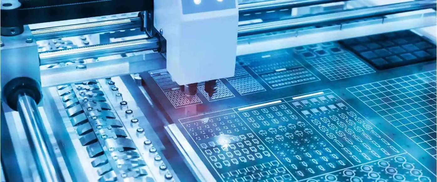
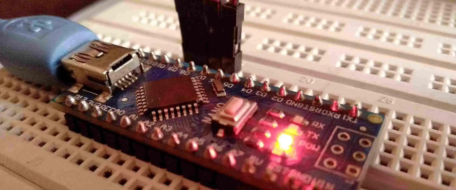
Manufacturing electronics involves more than simply design and manufacture. Making sure the board as well as electronic components is safe is a crucial aspect of PCB as well as electronics production. Electronics are now subjected to a variety of environmental factors as a consequence of advances in technology. Also, during the course of their lives, electronic components become susceptible to chemical and mechanical damage.

The functioning and reliability of components might be harmed by hazardous environmental circumstance. Conformal coating thickness has therefore proved a durable remedy for the harm brought on by different environmental dangers. For the conformal coating to be used in the PCB business, it is essential to comprehend its fundamentals. In order to learn more about conformal coating, this article aims to expand its knowledge base.

YouTube video

What Does Conformal Coating Thickness Entail?

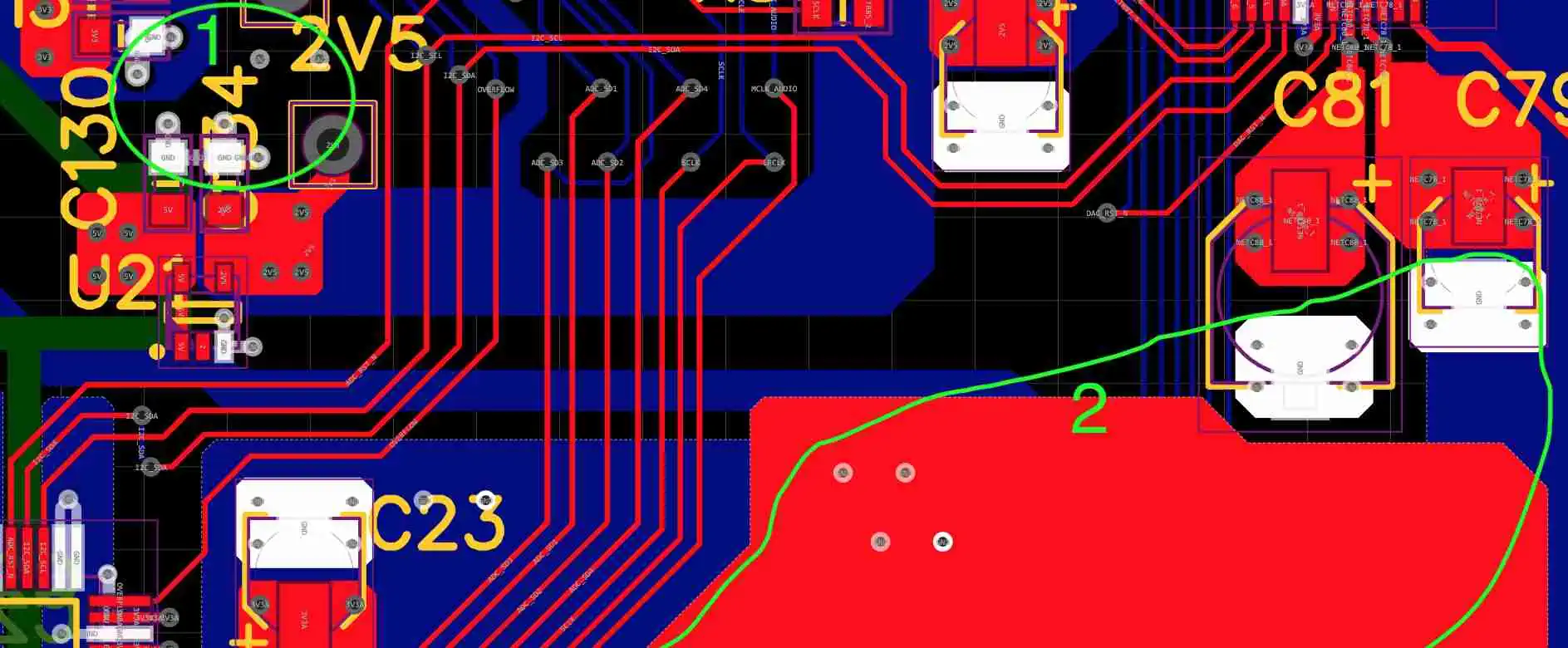
A circuit board, as well as its parts, is shielded from chemical deterioration by conformal coating. The polymeric thin layer is also included in the coating to shield a PCB board from outside impurities. The coating is often applied to a PCB’s surface.

Conformal coating also provides defense against contaminates including chemicals and moisture, as well as adverse environmental conditions. Moreover, this covering shields conductors from corrosion and short circuits. It provides insulation to reduce the mechanical and heat stress on electrical components. In the production of PCBs, conformal coatings remain essential, and they are utilized extensively in many different sectors.

Conformal Coating Types

Conformal Coating
Conformal Coating

There are several forms of conformal coating.

Urethane coating

High-solvent resistance is provided by this kind of coating. This is also a form of hard coating with high-strength. Urethane coatings offer superior chemical resistance as well as enhanced dielectric resistance. Moreover, polyurethane coating has a low-moisture permeability. Moreover, it resists abrasion.

Yet, this coat type has some disadvantages of its own. In high-temperature conditions, urethane resins do not really function very well.

Conformal coating of silicone

Silicone coatings remain clear and supple. They also offer excellent resistance to corrosion and dampness. Similar to urethane, silicone coatings are resistant to moisture. They are very resistant to heat stress. Silicone conformal coatings also function effectively in high temperatures. They have qualities that allow for light transmission. The dielectric resistance of silicone conformal coatings is not very great.

Acrylic coating

Solvent-based makes up this coating. Furthermore, acrylic resin covering has anti-fungal characteristics. Transparent, resilient, and hard describe this conformal coating type. Because acrylic is soluble inside a variety of different organic solvents, it is possible to restore acrylic coatings. Moreover, acrylic coatings have quick-drying qualities. Circuit boards, however, do not receive sufficient stress alleviation from it.

Conformal covering made of epoxy

Hard conformal coating describes this kind. Epoxy coatings are resistant to the damaging effects of solvents and moisture. They serve as 2 different thermoset combinations.

Due to its resilience against abrasion, chemicals, and moisture, epoxy resin coatings have been frequently employed. However, removing this covering without damaging the pcb board is challenging. This is due to a thermoset mixture shrinking during curing phase.

Paraxylene coating

Crystalline and linear polymer covering is present in proxylene. Materials for conformal coatings are these polymers. This particular conformal coating has high degree of transparency. Moreover, it may fit through small gaps.

What is the Significance of PCB Conformal Coating Thickness

FULL PCB MANUFACTURING Quote

Electronic items run at their highest efficiency thanks to the conformal coating thickness. Moreover, this coating provides the following advantages:

Decreased expenses for upkeep and replacement

The PCBs are protected with conformal coating. As a result, it lessens the harm done to circuit boards. As a result, pcbs require less replacement or maintenance. Also, more money and time may be saved by lowering the likelihood of damage. This happens because a little maintenance will be required.

Risk avoidance

When subjected to certain environmental factors, circuit boards can become damaged in a number of ways. Circuit boards are shielded from such harm by conformal coating, which is its major goal. As a result, conformal coating thickness shields boards from possible environmental risks such as heat and moisture. PCBs are also protected from dust, residues, and other pollutants by conformal coatings.
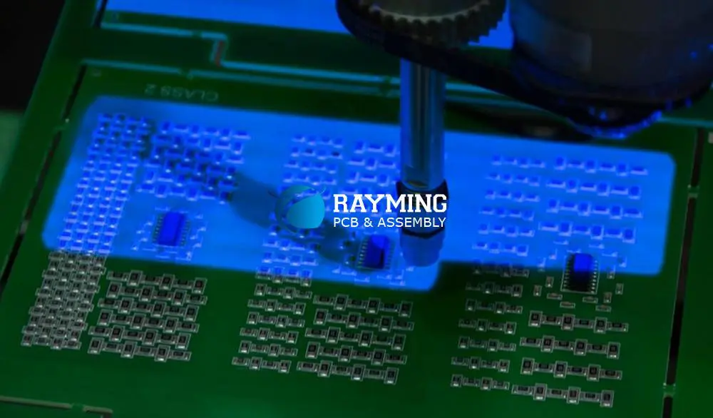
Improved inspection

UV coating as well as tracers are also part of conformal coating. Through the use of ultraviolet light sources, such UV tracers aid in coating evaluation. The light aids in detecting any flaking, cracks, or foreign objects inside the coatings.

Extreme thinness

Circuit boards and other gadgets have thickness and weight restrictions. There are several advantages to conformal coating thickness . This happens because it can fit properly on PCBs as well as devices that meet the most stringent requirements.

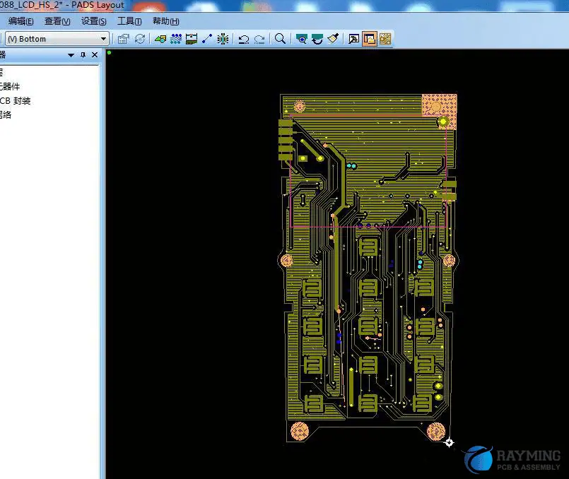
Process of Conformal Coating

The process of producing conformal coating entails a number of processes.

Cleaning

The conformal coating procedure begins with this stage. Cleaning aids in getting rid of various residues left behind from operator handling and soldering. Moreover, it eliminates contaminant-related residues. At this stage, cleaning methods include aqueous chemistry, solvent cleaning, and plasma cleaning.

Priming

A PCB is primed by having a preliminary coating called primer applied to it. This process aids in the creation of layers that will bond the coating and absorb it. The need for priming depends on the resin type.
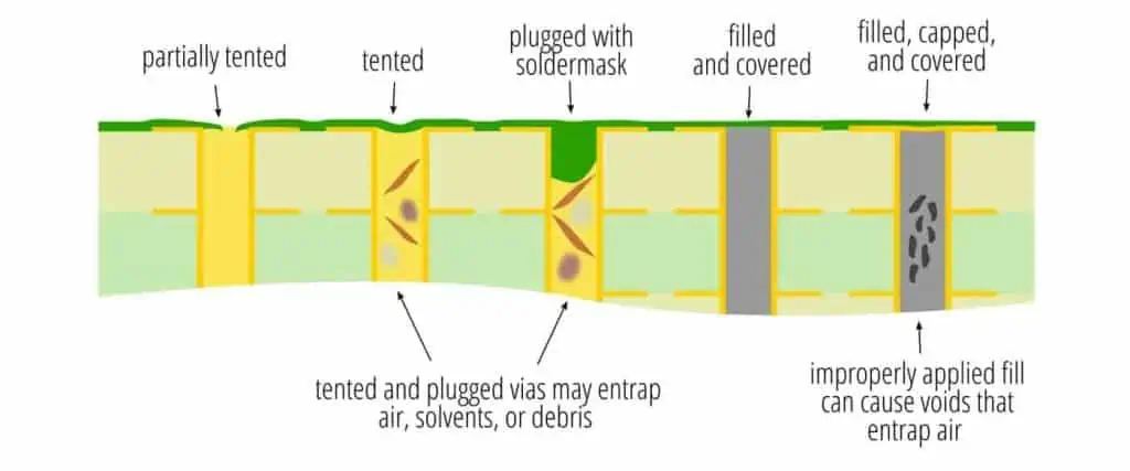
Masking

In components as well as certain board locations, masking prevents conformal coating from being applied. The PCB needs to have some uncoated spots. So, choosing the appropriate materials is essential to preventing masking failures.
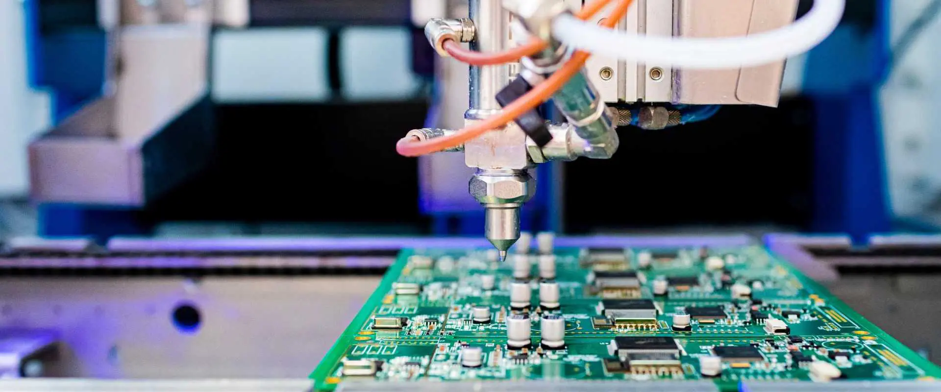
Application

Conformal coatings are applied at this process using a variety of application techniques. These techniques range from dipping to brushing.

Mask removal and completion

Masking must be removed after coating application. De-masking gets followed by finishing. Moreover, finishing aids in avoiding coating flaws and disguising leaks. Moreover, it validates standards and ensures coating quality.

Curing and drying

The circuit board’s coating is confirmed during drying, and it is then prepared for handling by operators. Moreover, this procedure might take a few seconds to many days.

Curing aids in ensuring that the coating acquires the required characteristics and protects the PCB while in use.

The most important phase in conformal coating is inspection. This process involves human examination, AOI, and UV light visibility.

Conformal Coating Certifications and Rules

PCB-circuit-board-waterproof-coating

Conformal coatings must adhere to certain laws and regulations.

UL746E

Consumer electronics safety is governed by the Underwriters Laboratories, a safety certification agency. This UL746E test examines the covered electronics for electrical and fire safety. This PCB is registered with UL under such a particular number when the conformal coating satisfies this test. Each PCB with an authorized coating must also be retested every year to keep its registration.

IPC-CC-83OB

Prior to becoming a civilian standard, IPC-CC-83OB is an IPC conformal coating thickness was a known military standard. This test primarily examines a coating’s appearance, flammability, and stability. Materials that satisfy the MIL-I-46058C standard would also satisfy the IPC-CC-830B criteria. The IPC-CC-830B is also updated often.

IEC 61086

Based upon supplier self-certification, this standard operates. IPC conformal coating thickness on circuit boards are governed by the IEC.

UL94V0

The conformal coating thickness on FR4 is examined for its flammability and self-extinguishing properties. The V-0 classification is the highest you can get. Nevertheless, there are more classifications, such as V-1 and V-2.

For environment protection, conformal coatings should adhere to strict legal requirements. Regulations for conformal coatings are established by the OSHA in the U.S.

Key Factors to Consider While Choosing the Most Appropriate Conformal Coating Thickness for PCBs

Operational Conditions

A PCB can benefit from conformal coating to prevent corrosion in whatsoever form. Thus, it is vital to take into account the coating’s capacity to shield the Circuit board from its surroundings. The temperature range as well as the PCB environment’s humidity must thus be taken into account.

The coating must also be suitable for usage in particular operational circumstances. Calculating the amount of daily exposure is crucial.

Electrical specifications

Typically, this insulating layer is produced using conformal coating. As a result, the most often examined electrical parameter remains surface insulation resistivity. Also, it’s crucial to take that measurement prior to as well as following coating. The coating should thus provide the necessary amount of insulation. The coating must also have a high dielectric strength.

Volume of production

The kind of coating used will depend on the manufacturing volume. Other elements, like as cure times as well as application technique, will be impacted by the manufacturing volume. For instance, any automated applications are better suited for mass manufacturing. Nonetheless, lower manufacturing volumes would be appropriate for hand spray painting.

PCB layout

Components which don’t require coating should be taken into account during PCB design. When preventing interaction with such locations, you can use a selective coating technique. The closeness of these components must also be taken into account.

Conclusion

In the production of PCBs and electronic components, conformal coating thickness is essential. It is among the greatest methods for creating robust and dependable PCBs. Moreover, this coating has superior electrical as well as mechanical qualities. As a result, the conformal coating thickness typically ranges from 1 – 5 mils. When selecting a conformal coating thickness, be sure to take key things into account.

Why the Circuit Board Cleaner is Important

circuit board cleaner

Clear circuit boards, particularly those found in personal electronics like laptops and smartphones, are frequently subjected to dirt as well as additional impurities. Electronics are subject to liquid spills from hands of users in addition to collecting dust and grime that enters via open gaps in casings. As a result, consumers of electronic products have an increased demand for circuit board cleaning as well as repair services.

Circuit board cleaning is a sensitive procedure which you should carry out with extreme caution in order to get back your electronics’ effectiveness. You could tamper with the connections, loosen a few pieces, or perhaps lose a few parts. You must choose cleaning detergents carefully while creating PCBs in order to prevent committing these errors.

How could Circuit Boards Become Dirty?

Electronic devices’ PCBs are fixed by the manufacturers, however they aren’t entirely safeguarded from dust as well as other impurities. Dust may readily penetrate ventilation and ports slots on casings and collect on the circuit boards. Additionally, the whirling motions of fans, particularly in large machines, might blast polluted air onto the board.

Remaining Products from Manufacturing

PCB circuit board cleaner

 In the past, producers of circuit boards used rosin-based fluxes that are activated. However, because these materials contain halogens like chlorine, leftovers left behind after soldering led to corrosion. As a result, manufacturers created several pcb board cleaner liquid techniques to take the place of the halides.

The majority of circuit board makers use no-clean fluxes, which contain organic acids like citric and adipic acids. Such organic acids are immediately broken down by that soldering heat and securely adhere to the solder, leaving a little corrosive.

This applied solder frequently covers some of the flux, preventing the heat required for breakdown. Following manufacture, a remnant of the partially degraded change is left on these soldered pieces. It might be preferable if you removed the debris to guarantee the PCB’s optimal performance for the duration of its lifespan.

The effect of work environment

 The main source of flux residues is carelessness after construction. Even after removing the debris from the PCB, you need still take environmental pollutants into account. For instance, it is very possible that particulates of dust will infiltrate your products as well as collect on PCBs if you operate in an excessively dusty environment.

The electronics appear to deteriorate more quickly in damp and dusty settings than in hot and dry ones. Even if you believe in the IP certification of your electronics, it’s essential to frequently inspect the PCBs to remove dirt before it builds up.

Inappropriate Use

ย Printed circuit board require a great deal of attention while operating because they are sensitive devices. Even while you might not be able to completely control the environment in which your equipment is used, ignoring simple handling and fabrication procedures might put the entire board at danger of contamination.

For instance, to facilitate heat dissipation, a PCB containing active components has to be enclosed in a well-ventilated case. If you’ve lined the air passages of the container with fins, you may prevent the dust from traveling directly to the printed circuit board. In comparison to a board in finned-type containers, one housed within an openly vented shell acquires pollutants more quickly.

YouTube video

Circuit Board Cleaner Types

Baking Soda

Baking soda may be used to remove corrosion from a PCB. Such corrosions are caused by acidic leaks and exposure to water that is salty. The soda’s moderate abrasiveness eliminates the corrosions while having no negative consequences.

Isopropyl alcohol

Since it is affordable and quickly evaporates, isopropyl alcohol remains a great instrument for cleaning electrical circuits. In addition, the beverage has less chemicals than traditional PCB cleansers. Always use gloves when working with isopropyl alcohol since it contains a high concentration (over 90%) that might harm your skin.

Deionized or Distilled Water

Since hard water contains ions that transmit electric current, numerous individuals choose deionized or distilled water since it won’t harm the circuit board. When not in use, make sure your water container is closed to prevent contamination from dust and dirt particles.

Compressed Air

Use brief bursts of compressed air to blast air into your gadget’s open spaces to remove dust that has gathered on surfaces including within circuitry without causing any disruption. You may open the equipment and use compressed air to properly clean the board when these openings are tiny.

Cleaning Equipment for Printed Circuit Boards

FULL PCB MANUFACTURING Quote

You’ll want an additional tool in addition to a circuit board cleaner to assist wipe down or brush off contaminants.

Microfiber clothes or lint-free towels

Towels can be useful for quickly wiping away cleaning solution. To reduce the possibility of leaving particles behind in your gadget, they must’ve been lint-free or made of microfiber.

A little paintbrush and brush with soft bristles also works nicely

For squeezing into tiny spaces in microwave pcb, little brushes are effective. However, to avoid the possibility of damaging the circuits, always ensure the bristles remain weak.

A desk lamp, an oven, or a blow dryer:

While the aforementioned cleaning agents can assist remove dirt, some might also leave liquids behind. Use a heat source to quickly dry it off to avoid damaging your board. When following instructions regarding how to wipe electrical circuit boards, this method is crucial.

Gas-Phase Cleaners

Boiling any chemical solvent that create steam is necessary for gas phase cleaning in order to dissolve impurities that have built up on PCBs.

As most solvents could be recycled once the contaminants are filtered out, the procedure is effective and environmentally benign. The pollutants you wish to remove, the solvent’s flammability, and its environmental friendliness should all be taken into consideration while choosing it. As this vapor can access the board’s difficult areas, the technique is more successful for the dense PCBs.

An Instructional Tutorial for Cleaning the Circuit Board

Step 1: Take apart your apparatus

To reach the Board, you must first disassemble the device using a screwdriver. Cables may need to be cut loose from the Board as well. Take images to help you with the entire reassembling procedure if you are unfamiliar with how the gadget is put together.

Step 2: Prepare the cleaning solution through combining distilled water and baking soda

You will need two teaspoons of this baking soda and a quarter of a cup of water. Mix both, until a very thick paste results.

Step 3: Using a Circuit board cleaning brush and the solution which you created in Step 2, begin cleaning the board.

Use the mixture sparingly to every corroded component and allow it to dry for 30 minutes.

Step 4: Thoroughly rinse the cleaning reagent using distilled water when it has dried.

Step 5: Spray your PCB with a phosphate-free home cleanser and let it sit for around 15 minutes. Using the cleanser and a Circuit board brush, eliminate any last corrosion.

Step 6: Wipe away any leftover dirt, dampness, and water using a lint-free cloth. Avoid wiping it downwards to avoid scratching it.

Step 7: To dry the leftover moisture, preheat the oven to about 1700, turn it off, then set the Circuit board inside for approximately three hours.

Step 8: Rebuild or reassemble the PCB and check to make sure it is operating correctly.

Why Clean the Printed Circuit boards?

pcb clean

When any user requires the circuit boards to function for a longer period of time, it is essential to preserve or clean the boards in a few years. The user must clean the circuit board on a regular basis to prevent overheating, which will increase power consumption, and corrosion.

Due to their increased susceptibility to external impurities and vulnerability, overheating has grown to be a serious problem in small-form integrated circuits. The printed circuit board’s dependability is prolonged when it operates in a clean environment free of dust and dirt.

Increase the Circuit Boards’ Reliability

As was previously said, the hardware must be properly shielded from impurities to maximize the dependability of every PCB.

Three things cause PCBs to become dirty and degrade performance: they are assembled or soldered in unclean conditions; flux residues were always left on boards even after the assembly; or the completed PCB is insufficiently protected from your environment while it is in use.

The user must completely remove all flux residues out from the PCB with no leftovers in order to maintain the integrated circuits’ long-term dependability and durability.

Avoid Corrosion of PCB Components

External impurities that come into contact with the pcb may function as insulation for the components thus obstruct airflow. Moreover, they can induce corrosion on  circuit traces and solder joints when exposed to aerosolized liquids or liquids.

The printed circuit board’s corrosive components may result in impedance problems and open circuits. Just covering any exposed copper portions with the conformal coating may stop pcb deterioration. Commonly employed and reliable defenses against corrosion and oxidation include epoxy coating, solder masks, as well as aerosol spray coatings.

Use Conformal Coating to Prevent Adhesion Problems

The coating on your PCB will come off whenever you leave any flux on the board prior to coating. In evenly spaced spaces inside this solder junctions, adhesion is much more frequent. Layers are also semi-permeable, which makes it simple for moisture to block flux deposits as well as eventually lead to corrosion.

Corrosion on a circuit board

Metal is typically used for the connections between every onboard component on PCBs. Metal components are vulnerable to corrosion. Similar to this, daily use can cause corrosion to harm any onboard metal utilized inside the PCBs.

The PCB may become even more damaged due to this corrosion, which will affect how well your hardware device functions.

Corrosion may be defined as the oxidation procedure resulting in rust when oxygen binds with metal, leading the loss of the metal’s chemical characteristics. Circuit boards ultimately experience corrosion and require treatment to prolong their lifespan.

Metals like gold, graphite, silver, as well as copper-nickel alloy have strong corrosion resistance.

What is the Cause of Circuit Board Corrosion?

Circuit boards may corrode for a number of causes, including ambient, galvanic, fretting, and electrolytic. The most frequent reason for metals within circuit boards to deteriorate is atmospheric corrosion.

In a process, metal ions join with the oxygen atoms in order to create the oxide when it is subjected to moisture, like oxygen. Galvanic corrosion, that occurs when various metal types are subjected to the electrolyte’s presence, comes in second.

In fact, the stronger metal will corrode more quickly when in touch with the weaker metal. Whenever ionic-contaminated moisture affects that electrical voltage between both traces, electrolytic corrosion results. This causes the neighboring traces to undergo dendrite development.

The final one is fretting corrosion, which occurs when solder-plated switches are closed in a way that wipes away the oxide coating upon that surface.

With time, considerable rust accumulates and renders the switch inoperable.

Solder flux removal from the circuit board

A heated metal that fuses two connections altogether is used in the process of soldering. The optimum method would be to use flux during soldering to avoid junctions from oxidizing by converting oxides into water and salt, then sealing in the change, once hardening is completed.

If soldering has occurred, solder flux could accumulate on chip pins. Whenever a manufacturer treats a PCB improperly, this problem is common, but it may be fixed. You’ll need a lint-free cloth, a Circuit board brush with soft bristles, and 90 percent isopropyl alcohol.

Use a bristles brush as well as isopropyl alcohol to gently clean your Board until this solder flux disappears. After you are happy with how your PCB looks, blot it using lint-free cloth.

You can quickly remove flux using anhydrous alcohol and perhaps a specialist flux ultrasonic pcb cleaner. The most economical approach, however, is to use very concentrated cleaning alcohol in place of these instruments and chemicals.

Conclusion

Contrary to popular belief, cleaning the circuit board using a circuit board cleaner or pcb board cleaner isn’t an exhausting task. The instructions and advice for cleaning the PCB have been covered in this piece of writing. Following these recommendations will guarantee that you use the proper PCB cleaning liquid process.

What are the Benefits and Manufacturing Processes of Stacked Vias?

PCB blind via fabrication process

The challenges of routing complicated components grow ever more challenging as current form factors of electronic products keep reducing the exact time that the physical component geometry becomes more dense.

This is frequently seen in designs using FPGAs with high pin counts as well as fine pitch ball grid arrays. This designing fanouts helps to have access to all the device’s pins. The common practice of using through-hole vias throughout high density systems may take up too much room to be useful. Effective routing of the PCB trace demands the application of new design methodology that applies to numerous present designs.

YouTube video

What Does Stacked Vias Mean?

Many vias are piled one on top of the other to form stacked vias. Every via would be first drilled but then metalized, keeping a tiny annular ring just at bottom and top to assure electrical connection. The annular ring has often been exceedingly small, a thinness of about .002″, necessitating highly accurate registration.

Stacked vias are more practical as well as adaptable for effective routing of the high density board since they may be stacked on the top of one another and occupy a smaller area on a Circuit board than the through-hole vias. Complete flexibility in the layer connection is made possible by the effective utilization of the stacked vias. Moreover, it lessens its parasitic capacitance that is often associated with vias. To guarantee a solid inter-via connection, manufacturing PCBs with the stacked vias necessitates more procedures.

The enhanced routing flexibility, even with marginally higher costs, frequently differentiates between effectively routing the design and having no way of doing so, leading to superior design solutions. Our engineering team anticipates that as the component densities rise and the surface area of the board continues to reduce, applying this layout method will become increasingly feasible and maybe even necessary.

Manufacturing Stacked Vias

Stacked vias need more stages in the manufacturing process than the staggered vias do. It is therefore more complicated. Here, a number of vias are piled on top of one another. They take up less room while connecting several layers. Before this stacking on the top of one another, each via undergoes drilling and then plated. On the bottom and top, two annular and narrow rings are available.

The lower one is utilized for electrical connections, whereas the upper one denotes exact registration. Three distinct acts make up the design:

  • Copper hole filling
  • planarization
  • Copper filling with stacked vias
  • further imaging

Electroplated copper is used to fill all stacked vias. It guarantees a reliable electrical connection as well as offers structural stability. On occasion, imperfections in the copper that has been deposited could be noticed. Here are some challenges explained:

Vias may become voids due to incorrect copper deposition. Inside the structure, such voids cause localized stress. This same dependability of stacked microvias may suffer as a result.

Electroless low-grade copper causes worse bonding in-between its target pad underneath the microvia as well as its base.

How Could Vias Affect PCB Design?

Vias really aren’t required when operating simple circuit boards, yet they’re crucial when working with multi-layered boards. Because of their flexibility in passing over and then beneath one another in different directions, stacked vias aid in creating high component densities on multi-layered boards but then also increase trace density. The numerous traces can connect with one another thanks to vias, which serve as vertical connecting elements.

The components of a surface mount would wound up being packed closely together on the circuit board whenever vias aren’t utilized for the process of routing the multilayered PCBs. The transfer of power and signals in-between the PCB layers is also facilitated by vias.

The effects or applications of stacked vias in Circuit board are covered here, along with several via forms:

Signal Routing

The majority of PCBs employ a thru-hole via positioned on the grid for the signal routing. Microvias are employed with highly dense boards, however buried or blind vias might be necessary for the denser boards.

Escape Routing

For the larger SMT components, thru-hole vias were typically utilized to provide escape routing, often known as fanout routing. Nonetheless, in some circumstances, microvias or blind vias could be employed. The via-in-pad is required for very dense packages having high pin-count ball grid arrays.

Power routing

As vias utilized for ground and power nets serves to conduct higher current, wider thru-hole vias are often employed here. Blind vias, however, are also an option.

Thermal regulation

In order to dissipate heat, a through is utilized to transfer heat from the component via its inner plane layers to which it is connected. Thermal vias are vias utilized for this capacity, and a bigger blind via or through-hole is needed to perform this purpose.

What are the Differences Between Staggered and Stacked Microvias?

FULL PCB MANUFACTURING Quote

This layer-by-layer method for creating a microvias of small aspect ratio makes them viable in different stacked applications, despite your initial reluctance to try include many blind and buried vias in your designs.

Buried vias are simply piled on the top of one another, or the blind microvia may be layered on top part of the buried vias. With an HDI PCB, this is known as the accepted method for spanning over many layers.

To guarantee firm contact when the following via in this stack is mounted and plated, any interior buried microvias present in the stack must be filled using conductive paste then plated over. The staggered microvias serve as an option to the stacked microvias in which the microvias present on the subsequent layers are usually offset from one another.

The board’s many layers are connected by staggered vias, although they are not in direct touch with one another. On the levels above and below, the position seems to be off. Considerably fewer procedures are required for staggered microvias. Such laser-drilled vias don’t really require copper filling since the subsequent drilled hole isn’t really next to the previous one.

Staggered vias link the board’s layers yet don’t come into direct touch with one another. On the levels above and below, its position is usually offset. Fewer design procedures are required for staggered microvias. Laser-drilled vias don’t really require copper filling since the subsequent drilled hole isn’t next to the initial one.

What are the Benefits of the Stacked Vias?

Many vias are piled one on top of the other to form stacked vias. Every via is initially drilled then metalized, maintaining a tiny annular ring just at bottom and top to assure electrical connection. The annular ring often is exceedingly small, as narrow as .002″, necessitating highly accurate registration.

Also, the stacked vias occupy a smaller area on a Circuit board than the through-hole vias since one via may be stacked on the top of the other and thus increases the likelihood of the high-density board becoming more flexible and practical.

Full flexibility for layer connection is made possible by the effective utilization of the stacked vias. Moreover, it lessens its parasitic capacitance that is often associated with vias. T o guarantee a solid inter-via connection, the fabrication of PCBs with the stacked vias necessitates more procedures.

Nonetheless, even with somewhat higher expenses, increased routing flexibility frequently represents the distinction between effectively routing the design and not being able to accomplish it,  resulting in improved design solutions.

With today’s downsizing as well as high-signal transmission performance and scalability in several applications, the stacked vias is a technique to further enhance density and size concerns when making PCBs, both of which are crucial.

The stacked vias might be the most dependable internal connection option when you’ve got blind vias having aspect ratios larger than 1:1 and if the drilling requirements span numerous layers.

Several vias are created together around a single center, also known as stacked vias and laminated buried and blind vias. The laminated vias with different centers are known as the staggered vias. In addition to reducing space and boosting density, stacked vias also offer more flexibility in terms of inner connections, improved routing capabilities, and reduced parasitic capacitance.

Different Via Forms

annular ring via
annular ring via

Through-Hole Vias

With the mechanical drill bit, the drilling of through-hole vias is through the Circuit board from the top to its bottom layer. It creates a conductive route that joins all of the PCB’s layers. Whilst through-hole vias were typically plating through-hole vias, certain vias may be the non-plating through-hole. PTH vias play a useful role for electrical connections between the various layers of the PCB, whereas NPTH is utilized for mechanical connections via connectors or screws.

Skip Vias

The skip via can be described as a PCB via that crosses numerous circuit levels without electrically connecting to any particular layer(s). Also, it can stop at one or even more separate HDI dielectric layer after penetrating at least two of them.

Conclusion

In summary, stacked vias are more practical as well as adaptable for effective routing of the high density board since they may be stacked on the top of one another and occupy a smaller area on a Circuit board than the through-hole vias.

Mastering the Art of ATmega328P PCB Layout: Best Practices for Optimal Performance

ATmega328P PCB Layout

The ATmega328P is an 8-bit microcontroller based on AVR RISC architecture widely used in Arduino boards. It has 28 pins, with many pins having more than one function. The chip has several features, including low power consumption and fast processing speed, that promote its use in many applications. It has six analog input pins, and its memory can reach 32kb. It also has 2kb of SRAM and up to 1kb of EEPROM. The clock speed of the ATmega328P stands at 16 MegaHertz, and it has 14 I/O pins. The minimum temperature at which it operates is 40 degrees centigrade, and the maximum temperature is 105 degrees centigrade. We must flash the Arduino bootloader onto the chip to program the ATmega328P onboard a custom PCB. The ATmega328P is a high-performance microcontroller with 32KB ISP flash memory with read-while-write capabilities. It is a popular choice for DIY Arduino

Power Supply Design

When designing the power supply for the ATmega328P microcontroller, it is essential to have decoupling capacitors very close to the die. For the devices possessing multiple pairs of the power and ground pins, it is necessary to have a decoupling capacitor for each pair of the pins. Ensure the main power supply has a tantalum or ceramic capacitor for stabilizing purposes. Additionally, you should properly regulate the power supply with no voltage spikes and add an extra 10uF capacitor between 5V and GND. It is also important to consider the power consumption of the microcontroller, which can be estimated by referring to the datasheet.

YouTube video

Component Placement

Another key factor is the arrangement of the components on the PCB. Component placement can impact signal integrity and circuit performance. Therefore, it is crucial to consider the components’ physical dimensions, the distance between them, and the closeness of sensitive components while putting them.

Since the ATmega328P is a surface mount component, the PCB is where it is mounted. Surface mount or through-hole components can be helpful with resistors, capacitors, and LEDs.

The distance between components should be taken into account when arranging them. For example, heat-generating components like voltage regulators should be placed far from delicate components to prevent thermal interference. Likewise, crystal oscillators and other parts susceptible to electromagnetic interference (EMI) should be apart from parts that produce EMI.

Signal Routing

While designing a PCB, signal routing is crucial, especially for intricate circuits like those utilizing the ATmega328P microcontroller. Signal routing entails joining the microcontroller’s pins to the printed circuit board’s sensors, resistors, and capacitors.

The traces’ length, impedance, and routing topology are significant things to consider when routing signals.

Trace Length:

To reduce signal latency and eliminate noise and interference, the length of the traces should be as low as feasible. Longer traces may bring noise into the circuit and degrade the signal. This is crucial for high-frequency communications in particular.

Trace Impedance:

To ensure the signals are appropriately matched, it is also important to consider the trace’s impedance. For example, maintaining signal integrity and lowering signal reflections that might lead to noise and distortion requires impedance matching. In addition, high-speed signals, such as those used for communication interfaces like SPI or I2C, require careful impedance matching.

Routing Topology:

You should carefully define the routing architecture to prevent signal crosstalk and ensure the signals route correctly. For example, two or more traces that are excessively close to one another and interact with one another might cause signal crosstalk. For high-speed communications, in particular, this might result in signal deterioration.

Avoid a high PCB noise or EMI area when routing high-speed communications since this can result in interference and signal distortion. This is crucial for delicate circuits that use sensors or analog-to-digital converters (ADCs).

Before beginning the signal routing procedure, it is crucial to consider the PCB layout to avoid signal routing issues thoroughly. Software tools may help to plan the routing topology and see the placement of components.

In general, signal routing is crucial when designing PCBs, especially for intricate circuits like those utilizing the ATmega328P. As a result, we can preserve signal integrity, minimizing noise and interference, leading to dependable and accurate circuit performance. We can achieve this by carefully arranging the routing topology, keeping the trace lengths short, and matching the trace impedance.

Grounding

Because it offers a constant reference voltage and helps reduce noise and interference, grounding is a crucial component of PCB design. Ground serves as the standard return path for electrical impulses in electronic circuits. The return current has a low impedance channel provided by the ground plane, which lowers noise and interference.

It’s crucial to appropriately connect each ground pin to the ground plane while constructing a PCB. The ground plane should provide a low-impedance channel for the return current, and the loop area should be minimal. The ground plane should also be isolated from the power planes to reduce noise and interference.

Electronic circuits are susceptible to ground loop issues, especially high-frequency circuits. We create a ground loop when there are multiple paths for the current to travel through the ground plane. This can disrupt the circuit and produce undesired noise. Therefore, it’s crucial to build the ground plane with a single connection point to the power source to prevent ground loops.

The usage of decoupling capacitors is a key component of grounding. To eliminate voltage spikes and high-frequency noise, decoupling capacitors are employed. In addition, to reduce the inductance of the power traces, they should be positioned as near as possible to the microcontroller’s power supply pins.

Furthermore, crucial to protecting delicate circuitry from electromagnetic interference is grounding (EMI). We can accomplish shielding by putting a ground plane between the EMI source and the sensitive circuits. This ground plane serves as a shield to stop EMI and guard against interference with the delicate circuitry.

In conclusion, grounding is an essential component of PCB design that we should not disregard. We can enhance the performance and dependability of electrical circuits by proper grounding.

Testing and Debugging

Various phases are involved in testing and debugging the ATmega328P PCB layout to ensure the circuit works as planned and to find and correct any problems or faults. Functional testing, visual inspection, continuity testing, functional testing, and simulation are some of these phases.

Visual Inspection:

Visual inspection entails examining the PCB for any visible flaws or faults, such as broken traces or pads, missing or wrong components, improper component positioning, or any other physical flaws. This can be done manually or with software tools that can find probable mistakes.

Continuity Testing:

FULL PCB MANUFACTURING Quote

Continuity testing involves measuring the resistance between several places on the PCB to determine the electrical continuity of the circuit. We can accomplish this with a multimeter or other testing tools. Therefore, examining the ATmega328P’s connections and pins for continuity and any other crucial parts like sensors, actuators, or communication interfaces is crucial.

Functional Testing:

Continuity testing involves measuring the resistance between several places on the PCB to determine the electrical continuity of the circuit. One can accomplish this with a multimeter or other testing tools. Therefore, examining the ATmega328P’s connections and pins for continuity and any other crucial parts like sensors, actuators, or communication interfaces is crucial.

Simulation:

We can test and debug the circuit using simulation before manufacturing. Software tools like LTSpice, Proteus, or Altium Designer, which can mimic the circuit’s behavior under various conditions, can be used for this. By simulation, we can find potential problems or faults in the circuit design and improve the layout and routing of the PCB.

Debugging:

Debugging the circuit is crucial if any problems or faults are found during testing so that the issue can be located and fixed. This may entail measuring the signals at various circuit points using a multimeter or oscilloscope, examining the voltage levels and waveforms, and contrasting the results with the predicted values. Debugging may also require changing the circuit design, such as altering the component values or the routing architecture to resolve the problem.

Testing and debugging are essential in creating the ATmega328P PCB layout. Circuit designers may ensure that the circuit works as intended and can detect and correct any problems or errors that develop by carefully inspecting the physical architecture, continuity, and functionality and simulating the circuit.

Popular PCB design tools for creating an ATmega328P layout

ATmega328P CHIP
ATmega328P CHIP

Popular microcontrollers like the ATmega328P are helpful in a wide range of projects. It is particularly well-liked in electronics. We apply it to many goods, from modest DIY endeavors to extensive industrial uses. Therefore, it’s crucial to pick the best tools to aid the design process while creating a circuit employing the ATmega328P.

Eagle PCB Design Software

For designing layouts for the ATmega328P, Eagle PCB design software is one of the most widely used tools among professionals and enthusiasts. Schematic capture, layout planning, and autorouting are just a few features and functionalities this robust tool provides. Eagle is a well-liked option since it is simple to understand and use and has a big user community that always assists with any queries or issuer.

Eagle features a sizable component library that includes the ATmega328P, making it simple to build and design circuits that employ this microcontroller. Also, it offers a potent autorouting tool that helps speed up and streamline the design process.

KiCad

A robust and well-liked open-source software package for designing printed circuit boards is called KiCad (PCBs). It provides various options and instruments for creating, revising, and evaluating PCB layouts.

The ATmega328P microcontroller, one of the many components in KiCad’s extensive library, is simple to incorporate into a PCB design. In addition, we ensure accuracy and dependability by automating the manually constructing of each component.

By drawing the circuit diagram of your design using KiCad’s schematic capture tool, you can help guarantee that all connections are accurate and that the design satisfies your needs.

The netlist generating function in KiCad creates a list of connections between the parts of your design automatically. Before moving on to the PCB layout, this can assist in locating faults or discrepancies.

You can produce a tangible representation of your design using KiCad’s PCB layout tool. KiCad offers a variety of design rules and tools to ensure your design complies with industry standards for signal integrity, power supply, and EMI/EMC compliance. You can put components and route traces between them.

KiCad offers a variety of design verification techniques, such as electrical rule checking and design rule checking (DRC) (ERC). These instruments ensure that your design adheres to industry standards and is error-free.

For building a PCB layout for an ATmega328P microcontroller, KiCad is a great tool overall. Electronics designers and engineers choose it because of its user-friendly interface, large component library, and potent design tools.

Proteus

For developing and modeling electronic circuits and PCB layouts, a common software program Proteus. The general procedures for utilizing Proteus to create an ATmega328P PCB layout are as follows:

Use Proteus to draw a schematic representation of the circuit. The ATmega328P microcontroller, any additional parts required for the circuit, and their connections should all be in this design.

Once the schematic is ready, you may use Proteus to produce a netlist for the circuit. You will make the PCB layout using this netlist.

Import the netlist created in the previous step into Proteus’ PCB layout editor. Using all the components and connections from the schematic, it will produce a new PCB layout as a result.

Place the components in the desired order on the PCB layout, leaving enough room between each one for routing.

To automatically route the connections between the components, use Proteus’ autorouter. As an alternative, you can route the connections manually.

After routing, you can produce Gerber data for the PCB layout. Finally, you can produce the real PCB using these files.

DipTrace

A well-liked PCB design program called DipTrace can be quite helpful when creating PCB layouts for the ATmega328P microprocessor. Due to its adaptability and simplicity, the ATmega328P microcontroller is frequently  in Arduino boards and used for various electronic projects.

Beginners can easily learn how to use DipTrace thanks to its user-friendly design. This can be quite helpful for enthusiasts who may not have much experience with PCB design.

To design the ATmega328P PCB layout, DipTrace has access to a wide library of components. Therefore, the time that would otherwise be necessary to create bespoke component footprints can greatly reduce by doing this.

Users of DipTrace can create design guidelines to make sure the PCB layout complies with predetermined requirements. This could aid in avoiding mistakes or problems throughout the fabrication process.

Users of DipTrace’s 3D visualization tool can see the PCB layout in a 3D setting. Before making the PCB, this can help to find any potential problems or design faults.

For the import and export of PCB layouts, DipTrace supports several file formats. This can be helpful when working with other designers or submitting design files to a manufacturer.

For developing PCB layouts for the ATmega328P microcontroller, DipTrace can be a useful tool overall. Both experts and hobbyists use it because of its user-friendly interface, extensive component library, design guidelines, 3D visualization, and import/export capabilities.

CircuitMaker

We can make complex electronic circuits and PCB layouts using the potent PCB design program CircuitMaker. Developing PCB layouts for microcontrollers like the ATmega328P is especially helpful.

Even those new to PCB design will find CircuitMaker simple to use. Users can rapidly develop and alter their ideas thanks to its user-friendly UI.

The ATmega328P microcontroller may be easily part of your PCB layout thanks to CircuitMaker’s built-in libraries. By doing this, you can design more accurately and save time.

Before production, users of CircuitMaker can model their ideas. This means you can test your idea before committing to a final version and make any necessary modifications.

Several people can collaborate using CircuitMaker, which can be especially helpful for complicated or large-scale projects. Users can collaborate in real-time while sharing their designs.

CircuitMaker is an affordable choice for PCB design because it is free and open-source software. For hobbyists or small enterprises that do not have a sizable budget for design software, this is very crucial.

Overall, CircuitMaker is a crucial tool for ATmega328P PCB layout because of its simplicity of use, integrated libraries, simulation capabilities, teamwork, and affordability.

The Ultimate Guide to Pic Programming vs. Microcontroller Programming

pic programming Vs. microcontroller programming

Microcontrollers are inexpensive and easy to get nowadays. They are often used instead of easy logic boards like counters to have more flexibility in design and save space. Some machines & robots use multiple microcontrollers, each dedicated to a specific task. So, Most modern integrated controllers are “System Programmable,” which means you can adjust the program without removing an MCU from its place. This article discusses the distinctions among ARM, 8051 AVR & PIC microcontrollers.

What is a Microcontroller Programming?

A microcontroller is like a small, independent computer that performs pre-programmed projects and communicates with other hardware devices. Despite its size & weight is negligible, it is a powerful device ideal for controlling robots or machines that require intelligent automation. A single microcontroller can manage small mobile robots, washing machines & security systems. Most microcontrollers have the memory to accumulate programs and multiple input/output lines to interact with other tools. So, these lines can read sensor data or control motors, among other things.

YouTube video

How does it work?

The Embedded controller is fast, but not as fast as a computer, so it executes every instruction quickly. When the energy supply is on, the control register enables the quartz oscillator. During the initial few milliseconds, as the setup is underway, the stray capacitance starts charging up.

Once the current level becomes maximum and the frequency of the quartz becomes stable, a writing bits process onto specific function registers begins. It syncs with the oscillator clock, and the electronics start working. All of this happens very quickly, in just a few nanoseconds.

Functions of Microcontroller Programming

Xilinx FPGA Programming

A microcontroller is like a self-contained process with memory, processor & peripherals. For example, the 8051 microcontrollers can be used in this way. Nowadays, most microcontrollers are integrated into machinery like cars, phones, appliances, and computer peripherals.

Advantages and Applications of Microcontroller Programming

Advantages

 Microcontrollers are inexpensive, small in size, and easy to use to integrate into any device. Learning to program microcontrollers is simple and not very complicated.

 We can use computer simulators to test and visualize the practical outcomes of the microcontroller programming. It is without buying the necessary components & chips for an integrated project. It enables us to see the works of our program and project virtually.

Microcontroller Programming Applications

Microcontrollers have a wide range of uses, including:

  • Mobile Phones
  • Automobiles
  • Cameras
  • Appliances
  • Computer Systems
  • Security Alarms
  • Electronic Measurements Instruments
  • Micro Oven

Types of Microcontroller Programming

ยท PIC Microcontroller Programming

PIC is a microcontroller element utilized in producing computer robotics, electronics, & similar devices. While the PIC is produced by Microchip technology and based on embedded system design, the code and data are stored in different registers to enhance input & output. The PIC has Internal memory, a dedicated microprocessor & data bus for managing all I/O functions and processes.

ยท ARM Microcontroller

ARM is the most widely used C language (commonly used for microcontroller programming) in integrated digital systems. Many industries prefer ARM microcontrollers because they offer great features to create products with excellent performance and appearance while being cost-effective. ARM microcontrollers are used in various applications, including Industrial automation systems, wireless networking & sensors & automotive body technology.

ยท 8051 Microcontroller

In 1981, Intel developed the 8051 microcontrollers. It is the 8-bit MCU that has 40 pins in a Dual Inline Package (DIP), 4kb ROM storage, two 16-bit timers, and 128 bytes RAM storage. The 8051 microcontroller has four 8-bit parallel interfaces that can be programmed and addressed according to the specifications.

ยท AVR Microcontroller

AVR stands for Alf & Vegard’s Processor. It uses the modified von Neumann architecture, which stores programs and data in separate physical memory procedures. It allows for browsing information from program memory using specific directions. AVR is not an acronym and does not represent anything specific.

ยท MSP Microcontroller

MSP is an abbreviation for MSP, which belongs to the family of microcontrollers produced by Texas Instruments. The Mixed Signal Processor is based on a 16-bit CPU and designed to be used in embedded systems that require low cost and low power consumption. The MSP’s architecture is designed around a 16-bit parallel bus with seven addressing modes – a reduced instruction set. It allows for shorter and more efficient programming code, resulting in faster performance.

A microcontroller is an integrated circuit (IC) chip designed to execute programs and control other devices or machines. It is a small device used explicitly for holding any other appliances or equipment, which is why it is referred to as microcontroller programming.


PIC Microcontroller Programming 

The PIC is a microcontroller developed by Microchip. Compared to other microcontrollers, such as 8051 and PIC, they are fast and straightforward to program. The programming of accessible and Peripheral communication has contributed to the success of accessible microcontrollers.

A microcontroller is a chip that integrates RAM, ROM, CPU, timers, and counters. Similarly, the PIC microcontroller also includes ROM, RAM, counters, timers, CPU, DAC, and ADC and supports communication protocols such as CAN, SPI, & UART for interfacing with other peripherals. It uses a Segmented Harvard architecture & RISC technology, making it faster compared to the 8051 microcontrollers based on the Stored-program computer.

Difference Between PIC Programming vs. Arduino                 

FULL PCB MANUFACTURING Quote

PIC stands for PIC, a term that is seldom used nowadays. On the other hand, Arduino is an open-source platform renowned for its user-friendly software & hardware. Both devices belong to the microcontrollers but have distinct working mechanisms and architectures. Therefore, their suitability for specific environments is determined by the application’s particular requirements. This article elaborates on the significant differences and similarities between PIC and Arduino, including their definitions, functions, architectures, advantages & limitations.

Differences between PIC Programming vs. Arduino

The following points outline some significant variations between PIC and Arduino:

ยท Arduino

As previously mentioned, an Arduino is the kind of microcontroller that comes in various forms, whether a 28-pin package or a greater modern SMD one. This compact integrated circuit houses all the components for computing projects, including a microprocessor, timer, memory & I/O ports for communicating with external digital devices. The microcontroller serves as the primary element on the Arduino circuit board, responsible for performing the device’s primary functions. The remaining components on the board, as well as the Arduino tool, assist in interfacing with the microcontroller. 

ยท Raspberry Pi 

It operates differently from an Arduino, functioning more similarly to a computer. The device contains a Broadcom System on the Chip (SoC) that includes a CPU & graphics unit (GU).

At the heart of the Raspberry Pi lies the Broadcom processor, which is linked to the board’s RAM, ports, & external storage. An American organization headquartered in San Jose, California, produces the CPU. The company name is Broadcom Inc. The company operates as a manufacturer, developer, designer & worldwide supplier of various semiconductor and infrastructure software products.

The primary purpose of a Broadcom Central Processing Unit is to execute a working system that oversees the fundamental operations of the computer, launches applications, regulates the USB, HDMI, and RJ45 ports, and delivers the interface for users to interact with.

The Raspberry Pi’s architecture allows it to perform tasks beyond the capabilities of the Arduino & its microcontroller. However, there are specific uses where a computer of this magnitude is unnecessary. For instance, consider the circuitry in a computer keyboard, which is utilized to monitor the set for activity and report keystroke events to the computer. Similarly, there is numerous microcontroller-controlled equipment in homes that complete their tasks affordably and efficiently.

ยท History

It is an open source electronics platform that comes with a tool package utilized to agenda the device’s hardware components. Its development aims to provide designers, hobbyists & students with an easily accessible platform for creating interactive and electronic-based objects, including automobiles. Massimo Banzi developed the Arduino concept, which is programmable and straightforward to deploy. On the other hand, PIC, known initially as Programmable Computer, was created in 1976 & is commonly used in integrated circuits.

ยท Structural design

Board processor for Arduino adopts the Harvard architecture, which employs separate memory for code and data. The memory is divided into data storage & data memory, and the flash program stores the data code. It consists of 2kb SRAM & 32kb Atmega328 MCU, with 1 kb EPROM that runs at a 16MHz speed. In contrast, the PIC MCU architecture features stack registers that save & return the work of Access Memory.

ยท Operation

Arduino uses digital read & write pins to handle input/output data. The mode pin sets the I/O mode, while analog read & write hooks take the input/output of analog data. The COM is responsible for configuring the bit rate for serial communication. In contrast, PIC is designed to support PDP computers in managing external devices. It has a user-friendly and straightforward operation, making programming a breeze compared to other controllers. PIC’s architecture is similar to Harvard architecture, and it can be easily programmed using flash memory.

ยท Qualities & Disadvantages

PIC Programming MCU is known for its adaptability and is less prone to faults. They operate on RISC architecture, making them highly efficient. Additionally, they consume minimum power and have a user-friendly, programmable interface, along with straightforward interfacing to all analog circuits. On the other hand, Arduino is an platform that allows users to construct their kits. Operating systems like Linux, Windows, and Macintosh support it. It is easy to understand, making it ideal for beginners. However, it should be noted that the code length of Pic controllers is limited due to its RISC architecture.

Difference between AVR and PIC

ic programming services

An MCU is a compact Integrated Circuit (IC) that operates like a small, standalone computer & is designed for performing specific tasks in embedded systems. It consists of a processing unit, a small memory amount (RAM, ROM, etc.), and Some I/O for peripherals & timers. Two popular types of microcontrollers are AVR and PIC, which have varying architecture, instruction sets, speed, cost, memory, power consumption, bus width, and other features. In the following sections, we will explore the differences between these two microcontroller families in greater detail.

ยท AVR micro-controller : 

Atmel corporation micro-controllers were first introduced by Atmel in 1996 and are based on the ISA, also known as Advanced Virtual RISC. The first microcontroller in the AVR family was the AT90S8,515. AVR MCU is famous for its affordability and is widely useful in various robotic applications.

PIC microcontrollers, on the other hand, were by Microchip Technology Inc. in 1976. The acronym PIC stands for Programmable Intelligent Computer. These microcontrollers are based on Harvard architecture and are famous for their efficiency, minimum energy consumption, and ease of programming. They have reasonable prices and are useful in diverse industries.

The abbreviation “PIC” originally stood for “Peripheral Interface Controller,” and Microchip produced this type of MCU. Moreover, It is also easy to program and interface with various peripheral devices.

 AVRPIC
01.AVR is an acronym that stands for Advanced Virtual RISC microcontroller.PIC is an acronym that stands for Peripheral Interface Controller microcontroller.
02.The AVR microcontroller has a bus width of either 8 or 32 bits, which means it can process information in chunks of either 8 or 32 bits at a time.The PIC  MCU has a bus width of 8, 16, or 32 bits, which determines the amount of data it can process simultaneously.
03.The AVR microcontroller is compatible with communication protocols such as USART, UART, SPI & I2C.The PIC microcontroller is compatible with communication protocols, including PIC, USART, UART, Cab, LIN, Ethernet & SPI.
04.The AVR microcontroller’s speed is measured at one clock per instruction cycle.The speed of the PIC microcontroller is measured at four clocks per instruction cycle.
05.The AVR microcontroller uses the RISC (Reduced Instruction Set Computing) instruction set architecture.The PIC microcontroller uses specific characteristics from the RISC (Reduced Instruction Set Computing) instruction set architecture.
06.The AVR microcontroller is designed based on Harvard architecture.The PIC microcontroller is designed using a modified Harvard architecture.
07.The AVR microcontroller comes in different families, which include Tiny, Xmega, Atmega & special-purpose AVR.The PIC microcontroller comes in various families like  PIC16, PIC24, PIC18, and PIC32.
08.Atmel is the company that manufactures the AVR microcontroller.The company Microchip manufactures the PIC microcontroller.
09.The AVR microcontroller is a cost-effective or efficient option.The AVR microcontroller is an affordable option.

Differences between PIC Programming and Arduino

FPGA programming

Raspberry Pi and Arduino are great educational equipment for students, hobbyists, and beginners. However, there are some differences between the two that should be noted.

  • Arduino is a microcontroller circuit board. A Raspberry Pi PCB is a microprocessor-based mini-computer (SBC).
  • The MCI on an Arduino board comprises the RAM, CPU, and ROM, while Raspberry Pi has the features of the computer, memory, graphics driver, storage, and connectors on the board.
  • All the additional hardware on an Arduino board is for power(energy) supply & IO connectivity.
  • Raspberry Pi requires an operating system, while Arduino does not require any functional system. 
  • Raspberry Pi is shipped with the whole functional system is Raspberry Pi. However, you can also use other operating systems. Linux is perfect to use as it is the recommendation of Raspberry Pi. Additionally, It is possible to install Android on Raspberry Pi as well. On the other hand, Arduino doesn’t require a functional system. It only needs firmware instructing an MCon U on what project to perform.
  • Arduino clock speed is 16 meg Hartz, whereas Raspberry Pi has a much higher clock speed of around 1.2 GHz.
  • Raspberry is suitable for producing software Apps using Python. But Arduino is ideal for interfacing with sensors & controlling LEDs.
  • Connecting sensors & LEDs to PCB Raspberry Pi is possible through the 40-pin GPIO. It combines electronic components like buttons, sensors, motors, and LEDs, among others. Similarly, Arduino’s GPIO is Digital IO for digital input & output and Analog IN for analog information. So, Both boards offer options for hardware programming and control.
  • Arduino Shields have plugged in the Pin headers; you can add dedicated features or functionalities such as an Ethernet Connection, Motor driver, SD Card, Wi-Fi, Cameras, Touchscreens, etc., to Arduino. On the other hand, Raspberry Pi is a self-contained board, and you can add external hardware, such as Touchscreens, GPS, RGB panels, etc. 
  • The power needs of Raspberry & Arduino differ significantly. While both are powerable by USB, Raspberry Pi requires more voltage than Arduino. Therefore, a power adapter is essential for Raspberry Pi, whereas Arduino is powerable from a computer’s USB port.
  • Sudden power interruption can cause harm to the software, hardware, or applications of Raspberry Pi. On the other hand, if there is an off power for the Arduino, it will restart automatically. Therefore, it is necessary to properly shut down Raspberry Pi before disconnecting the power to avoid any damage.
  • You can create your own Arduino board using the hardware & software files. However, Raspberry Pi is not open-source, so it isn’t possible to make you have a Raspberry Pi board.
  • The Arduino UNO board costs $23, but there are many clones for a minimum of n $4. On the other hand, the actual Raspberry Pi was priced at around $35, while the Raspberry Pi is available at different price points ($35, $55, or $75) depending on the memory configuration

How to decide between PIC Programming and Arduino?

ic programming

Between the two, it is essential first to determine the requirements and objectives of your project.

  • As per the above discussion, it can be concluded that Arduino is good for performing repetitive tasks such as garage doors, turning lights on and off, reading temperature sensors, and controlling motors according to user needs.
  • The previous discussion highlights that Raspberry Pi is suitable for performing various tasks, driving complex robots, playing videos, connecting to the internet, interfacing with cameras, and similar applications.
  • An illustration of using Arduino is to build an application that tracks Humidity & Temperature readings from the DHT11 Sensor and exhibits the outcomes on the LCD screen.
  • If your objective is to track the Humidity & Temperature data from a DHT11 Sensor, email with readings, compare the data with an online weather report, and exhibit the outcomes on the LCD screen. So, Raspberry Pi would be the appropriate option.
  • In basic terms, beginners employ Arduino beginner-level projects and speedy electronics prototyping. In contrast, Raspberry Board Pi is suitable for more complex tasks that the Pi can effortlessly manage.

The Science behind GND in Circuit: What You Need to Know

4 layer gnd in circuit

GND stands for Ground. A common or shared return route of electrical current to the power source that enables the completion of the circuit refers to the ground in both electrical and electronic circuits. It is in DC circuitry with negative, positive, and ground sides. Also, in switching the current network with the neutral, phase, and ground.

Since it’s a non-energized terminal and even directly with the ground, it may also see as a reference node in a PCB for measuring voltages. Also, it may serve as a safety measure. This ensures that if a circuit leakage current or an atmospheric lightning discharge occurs, the dangerous energy can travel toward the Earth.

YouTube video

ยท What Is GND In-Circuit?

In the field of electronics, a point or a location in a PCB is an electric reference point by convention. The voltage at such a reference point, sometimes referred to as Ground or GND, is zero volts. Measurements of voltage are relative measures. In other words, the measurement of voltage has to be contrasted to some other circuit point. If not, the measurement has no value.

All electrical circuits have to be sealed unit to work; this means that it must always have a path for the current to go back to the supply. No matter how complicated a circuit gets, the current will always have a way to return to its source, whether it is a plane or a trace.

This reference end often serves as the starting point for all subsequent voltage measurements inside the circuit. Not all measurements of voltage, nevertheless, are by using this reference end.

These return channels are “ground” in practically all circuits. The issue here is that “ground” is the circuit’s reference point, which is problematic.

There isn’t such a thing as a perfect zero voltage. Hence the reference coordinate is essential. Voltage measurements are always relative to a reference point in the PCB design. This does not need to be present at a return route. In truth, any point in the circuit might theoretically serve as the reference point, but for reasons we’ll discuss shortly, some points are preferable to others.

ยท Earth Ground 

4 layer pcb ground plane

The point of reference for all of the electric wires in the homes is Earth (the dirt beneath the feet, not the planet). This is a limitless supply of electrons. Practically speaking, the way that this return line is “connected” is just by burying a metal pipe or rod in the earth. Then try to ensure that all of the homes’ “ground” wire firmly links to it.

ยท Chasis Ground

The metal casing of a gadget is useful to define a point of reference for an electronic circuit, giving rise to the name of this particular form of ground. Safety is the first consideration while choosing the enclosure’s chassis and the ground as points of reference. Almost usually, the potential of our bodies is on Earth. Suppose that the user is about to do the laundry and that the chassis of the washing machine is with the earth plug of the outlet. All of the electronics within the machine link to the earth’s ground or chassis.

Once more, if we consider return pathways, we can observe that in such a scenario, the earth ground and chassis are part of a returning route to the source of AC. This prevents an electrical current from flowing into your body. This happens due to a potential gap between the body and the washing machine.

ยท Signal Ground

It simply defines the circuits’ reference node on the PCBs and is among the most used designation. A ground plane or sheet typically use to physically implement it. So the PCB design may have a quite low impedance returning the route to the source of power. This is crucial because if it’s not done, different “grounds” over the PCB can have different potentials. And the PCB might fail or just stop working altogether.

ยท Analog And Digital Grounds

As the states of the digital signals fluctuate, current spikes are in digital circuits. Current peaks are once more produced in the analog circuits when the current load fluctuates.

Even though there are several methods for doing correct grounding, it is crucial to distinguish between the “noisier” digital returning currents and the “lesser-noisy” analog returning currents whenever it relates to mixed-signal earthing. The generation of noise inside circuits owing to ground current flow is preventable by this isolation of the grounding.

When these ground currentsโ€”which you might conceive of as shifting currentsโ€”are directed to ground-returning pathways, noise is produced by voltage fluctuations (remember Ohm’s Law). You may be familiar with the phrase “a loud ground.” On local circuits, this noise might impair delicate signals. For system, test, and design engineers, grounding has long presented significant challenges.

A “star,” earth, or ground is one potential grounding method that may be useful in certain circumstances. This way of thinking is based on the idea that every voltage in a network refers to the same ground point.

On paper, the sole grounding location and star ground approach appear to be a brilliant idea. Based on how sophisticated one’s design is, it may be quite challenging to implement in practice. Using a ground bus bar is an alternate approach.

Nevertheless, remember that if a design employs a single common ground plane, return currents may be regulated by a good PCB layout. So there’s typically no need to physically separate the digital and analog grounds.

ยท Common GND In-Circuit Errors

For newcomers, a three-end DC energy source may seem somewhat confusing. There are three terminals on this power source: the positive (+) terminal, the negative (-) terminal, and the ground or GND terminal. The earth ground or ground terminal is physically attached to a chassis, which is then linked to the earth wire inside the power adapter. It is with Earth directly through the three-prong socket.

Beginners frequently make the error of connecting power between the GND and the positive (+) connections. No electricity will run since this improper connection prevents the current from going back to the electrical supply, which is where it gets its energy. Connecting the power between both the negative (-) and positive (+) terminals is the right connection.

ยท Electrostatic Discharge (ESD)

Your test device’s grounding also aids in the prevention of a discharge of electrostatic or ESD. Whenever a statically electrified body touches the test apparatus, ESD happens. Certain testing tools are extremely sensitive and can be quite susceptible to ESD incidents.

ESD shielding for the ICs is adequately provided by grounded mats. This also refers to ESD mats, wrist straps, and grounded chairs. This is because they ground you before you touch any sensitive electronic component, discharging whatever static charge you might have on the body. While working with Circuit boards and ICs, the majority of technicians and engineers also put on ESD-safe jackets as additional security against potentially harmful parts and equipment.

Common GND In-Circuit Problems

FULL PCB MANUFACTURING Quote

The voltage differential among “grounds” on several decks or areas of a yacht, for instance, might be in the volts of tens. When working on a ship deck, there are noticeable voltage differences between the ground on the electric extension cord and the person utilizing the long extension lead. Similar issues arise on airplane surfaces when they travel at extremely high speeds through the magnetic field of the Earth. As a result, there is a little voltage differential between the points of ground. 

 A voltage produces as the current runs through the substance. Impedance is present in conductors, wiring, junctions, as well as in soil.

While designing a circuit, it is best to keep all grounded nodes close to one another and steer clear of loops and numerous earth loops. Frequently, the power enters at this location, or the primary decoupling or smoothing capacitors with a chassis at this location.

High gains equipment, like amplifiers, will have a lot of current flowing via the ground wire. It becomes crucial to ensure that all these grounds aren’t with the amplifier’s input stages. If not, oscillation happens. Only at a single stellar ground should the output and input stages come together.

ยท Ground Loops

In high-output audio systems, connecting equipment with an independent mains power supply can cause ground loops. A mixing panel and a PA device, for instance, each with a separate main supply power source. Significant hum issues are there when the metallic grounding screen within the audio wires forms a loop with various mains earth.

When the demands on each stage are in a three-stage mains power system, the point of neutral should have zero potential. Rarely is this the case. Voltage variations, among other phases, will result from large current activity on one side, which will lead the neutral current to “float” higher. 

Do You Really Need GND In Circuit?

All circuits require a “ground” because every electrical system requires at least one return route to the power source. This “ground” is typically also useful as the referencing node for measuring all of the network voltages. Nevertheless, not every circuit connects to the line voltages (such as battery-powered electronics). Hence not every circuit will require earth “ground.” More accurately, a return channel via the earth. Similarly, a chassis returning route is not necessary for the safety of electronics in non-conductive environments. What we want is the ability to rename these roads to prevent misunderstanding with the ground.

Designing a Digital Thermometer PCB: A Comprehensive Tutorial

thermometer pcb

Unlike conventional thermostats, digital thermometers are unaffected by damage at extremely high temperatures. Thermocouples are frequently used by designers in industries to measure high temperatures. After you have the schematics of circuits for the Circuit layout of the digitalized thermometer, this post will assist you in understanding how to proceed.

Whatever components you utilize are entirely up to you. We would, nevertheless, provide you with some advice regarding some ideal electronic parts. You might be considering making your digital thermometer.

We’ll go through each step so you can successfully create a PCB digital thermometer.

YouTube video

1.ย Finalize Your Thermometer PCB Circuit Schematics

A digitalized thermometer may require for personal, professional, or industrial applications. You may require high-temperature resistance if you’re developing the schematics of PCB for industrial use. A microcontroller like the ATmega16 MCU may be used to measure temperatures up to 1024ยฐC.

For the digital thermometer to detect high temperatures, you might additionally need to utilize thermocouples. K-type thermocouples are the most popular kind. Given that it is dependable, accurate, and affordable, you are probably already utilizing it. Also, you ought to make use of ICs like the MAX6675 IC. It will digitally transform the K-type waveform and inherit cold-junction correction.

Since the device is cold and the thermocouple tip is not (0ยฐC/32ยฐF), cold-junction correction in electronic thermometers compensates for the absent thermoelectric voltage. You can get digital signals from the MAX6675 Integrated Circuits that are 0.25ยฐC precise. You may utilize seven-segment displays to obtain the display. Electronic thermometers can use with thermistors for household usage.

2. Make Layout of Thermometer PCB

Well, so you are ready to start constructing the digital thermometer PCB design once you complete the schematic of the circuit and create it in your preferred program. The PCB’s trace architecture and component arrangement are modeled by the schema.

Moreover, the PCB layout program will convert all traces, wires, and components into a format of PCB, speeding the process of designing.

It is essential to ensure that every schematic sign in an electronic thermometer corresponds to a PCB layout. The PCB layout specifies the physical size of the components as well as the location of copper pads or through-holes. You will next begin routing the cables for your custom-designed digital thermometer. Both manual and automatic routing options are available.

When all of the routings are finished, labeling the components or signs is a smart idea. The tags then transfer to the Circuit design and eventually appear on the finished PCB. Also, you may arrange electrical components across every area on the Circuit for the thermometer. It attests to the shortness of the conduction lines and traces. Long traces may amass significant quantities of electromagnetic waves, which can produce interference and noise.

3. Etch Your Thermometer PCB

A4 shiny or picture paper can use to print the PCB thermometer using a laser printer. To make sure the printout is on the article’s positive side, one must take a mirror image of it. Also, must choose the black output color in the printers and PCB design options.

Cut the copper sheet for the PCB thermometer after that. Depending on the PCB layout size, you can use a hacksaw or a cutter. To scrape the copper off the PCB, use steel wool or abrasive sponges. Any oxide or photoresist layer that may be on the Circuit board will be removed. The digital PCB thermometer printed design will then be transferred from the A4 glossy paper to the Circuit board.

Keep the printout and board in the proper alignment at this phase. To maintain these in the appropriate place, you can apply a piece of tape. The PCB design of the digital thermometer printout will then applies to a copper sheet using an iron. The reverse of the A4 Glossy paper will expose to the heated iron for between five and fifteen minutes. The glossy paper’s ink will transfer off the PCB by heat.

4. Drill Vias Into Thermometer PCB Sheet

Vias could have been employed while creating the PCB for the digital thermometer. The electronic impulse can travel along these routes as it passes through various circuit levels. If you’re new to PCB design or designing them at home, you can use through-hole vias. For drilling needs, you need to get in touch with a PCB maker if you’ve created hidden or blind holes.

Several vias cannot drill at home. For these objectives, PCB makers utilize particular automated drilling equipment. You’ll see that any PCB designing software can output a drill document. You must create the drill document, which includes all the specs for the holes needed for the finished PCB manufacture.

There’s no special method you may use if you want to drill. But, you must abide by the limitations on minimum diameter, maximum area ratio, and hole proximity. The maximum area ratio is obtained by dividing the thickness of the PCB by the tunnel width. Adjacency refers to the shortest distance that can allow between the edge of a hole and the nearest neighboring hole.

5. Solder the Electronic Components

Now, assembling the components of the thermometer PCB is a very straightforward process at this point. Resistors and Capacitors might also use as a starting point, then a battery connector and a thermistor, and finally ICs and screens. Always remember to install any DIL plugs on the PCB of the digital thermometer at the very end if you’re using any.

Be cautious while soldering of ICs if DIL plugs are not being used, though. Before securing the subsequent bolt, the pin must have cooled. They can harm small wires in the Integrated Circuits and are extremely heat-sensitive, thus the reason. Moreover, never leave the solder on an electric pin for longer than 4 sec. Before beginning to solder the remaining nails, wait a further five seconds. You can connect wires to switches and thermistors even if you’re not adept at soldering. The goal is to prevent soldering and put them on the chassis. You have the option of inserting the thermometer Board inside a plastic ring after soldering. The digital thermometer appears more polished as a result.

6. Test Your Final Thermometer PCB

Now that the PCB for the digital thermometer is complete, it’s time for a check for any assembly flaws. You may test the PCB’s functionality. On simulation, you may verify what LED lights up when the simulation is first started. To ensure the digital thermometer PCB is operating properly, you may add an indication LED to the circuit.

You may supply power to the PCB and see if the indication LED illuminates. To look for any open circuits or sparks, you may also insert the DMM’s probe between various circuit locations. These techniques are conventional. Thus beginners should avoid using them. PCB producers employ cutting-edge methods like beds of nails and in-circuit testers.

Contact RayPCB for Thermometer PCB

FULL PCB MANUFACTURING Quote

Don’t move if you feel that all of these processes are too lengthy and that you don’t have much time. We also offer the ideal choice for you. Just search for a knowledgeable PCB maker. They’ll need specialized equipment and tools to complete search all of these processes.

All you have to do is search online for PCB manufacturers, then submit a request on their site. You must submit documents like drill data and Gerber. The manufacturer uses these properly to create the PCB for the digital thermometer.

Conclusion

These are the seven procedures you need to know before starting to build the PCB for the electronic thermometers. You must create circuit diagrams using programs like Altium Design and Eagle. Then transform these into a Circuit board and print it out.

Use a heated iron to transfer the electronic thermometer printing on the copper plate. Then arrange the components, drill holes, and solder them. Test the finished PCB. Nevertheless, if you want PCB facilities, get in touch with us; we can offer the necessary technology, supplies, and services. Call or email us right away.

Avoiding Top 12 Common PCB Soldering Troubleshooting Mistakes

Soldering Circuit Boards

Making soldering errors is a common occurrence, especially when dealing with many PCBs. As a result, it is possible to encounter various soldering flaws while carrying out such tasks. Even experienced technicians can make mistakes, such as overheating or underheating a pad or applying too much and too much solder. To prevent these mistakes, it is essential to understand how to recognize defective solder joints.

YouTube video

Soldering Troubleshooting

Identifying soldering defects requires a trained eye. A correctly soldered joint should be clean, symmetrical, and have a concave shape compared to the neighboring joints. A defective solder connection will be disorganized and have a physical abnormality, like a swelled shape or a long stem. Here are the 12 Typical soldering mistakes and the resulting problems:

1. Disturbed Joint

One prevalent issue found in columns and rows of soldered connections is the disrupted joint. It is recognizable by its swollen, distorted, and occasionally flakey texture. The main reason for unsettled joints is any form of movement during the soldering process. For instance, if the board is positioned on an irregular surface and vibrates or tilts while the solder is applied, the joint can become disturbed or lose its integrity. Additionally, if the board experiences any movement or vibration while the solder is drying, it can also cause a disturbance in the joint.

Confusing Disrupted joints with cold solder connections is a common mistake. Although they have a Resembling appearance, the causes of these issues are different. In certain situations, reapplying heat to the joint & letting it solidify without any disturbance can fix the problem. 

In the coming days, ensure each joint is secure and stable when applying solder.

2. Cold Joint

A common issue observed on a freshly soldered circuit is the presence of icy solder joints. These joints are recognizable by their uneven and sometimes undefined appearance. These joints are typically the result of insufficiently melted solder during the application process. In addition to their unappealing appearance, cold connections are challenging. They do not provide adequate bonding and are prone to developing cracks over time.

Repairing an icy joint is possible by applying heat once again. It can be achieved by using a hot iron. Additionally, if there is an excess volume of solder on the joint, it can be removed by using the pointed end of the hot iron. To avoid cold joints from forming in the future, it is crucial to ensure that the iron is heated to the appropriate temperature before utilizing the solder.

3. Overheated Joint

SMT-Through-Hole-Soldering

One of the most noticeable blemishes that can occur on a set of newly soldered joints is the Burnt joint. This type of common forms when too much heat is applied during the soldering process. In contrast to cold joints, which result from Inadequate heat, overheated joints occur(happens) when the iron is excessively preheated before application. These joints have a burnt appearance with a lumpy and misshapen structure.

To rectify the issues caused by overheating during the soldering process, a burnt flux and its surrounding area can be scraped off using the tip of a PCB working tool. If necessary, a solution like an isopropyl alcohol can eliminate a burnt flux. The ideal way to utilize alcohol is by using a small toothbrush.

Overheated joints can be difficult to fix, making it important to avoid them at all expenses. To prevent this issue on typical days, it is crucial to ensure that the iron is heated to the appropriate temperature and to check twice that the connections are clear before starting the soldering process.

4. Insufficient Wetting of the Surface Mount

Failing to heat both the pin and the cushion during a soldering process can result in an inadequate surface mount, where the support elements do not flow on a solder cushion. This issue can be identified easily if irregularities are present across a mount’s row. If different props have correctly streamed on the surface while 1 or 2 extra mounts have retained their actual pin composition, it is likely due to an inadequately wetted place.

To correct an inadequately wetted pad during the mounting process, preheat the iron point to the required temperature and then implement it into a solder pad. Add more solder to the place, allowing it to flow and dissolve into the design with the pin’s solder. To prevent this recurring issue, heat the Pad earlier than heating a pin during future soldering applications.

5. Insufficient Wetting of the Pad

Insufficient wetting of the solder pad in the soldering procedure results in an uneven joint without bonding strength. Typically, in such cases, an ample amount of solder would have moistened the leads, but the pad absences the important bonding power. A common cause of this issue is applying solder to a soiled circuit board, where the dirty circuit board prevents proper bonding. Additionally, if the Pad & pin lack adequate heat during the application, the place may finish with insufficient wetting.

To fix the issue of an improper wetted pad, heat the iron tip to the appropriate temperature or keep it at the base of the joint. Allow the solder to flow onto the surface, ensuring it wets the surface properly. To restrain this issue from happening in the future, ensure that the board is clean before starting the application and preheat the Pad and pin to the required temperature level.

6. Insufficient Wetting of the Pin

If both the pad & pin exhibit poor wetting, it is likely due to insufficient heat treatment of the pin. It commonly occurs when the plug is not getting heat sufficiently, preventing the solder from flowing into place.

To address the problem of an incompletely wetted pin, heat the iron trading point to the required temperature and apply additional solder. It is important to touch the Pad and the hook with the iron tip during the reapplication process to condition these elements for the appropriate application. To avoid this problem in the coming days, ensure that the pin and the Pad are heated to the right level during soldering.

7. Solder Starved

A joint that has an insufficient amount of solder is a solder-starved joint. Such a joint lacks the strength to perform its intended function and can lead to board failure if not addressed. Even though an insufficient solder joint may exhibit good conductivity, the board would still not be safe to use until the issue is resolved by adding more solder to the affected joint.

To fix a solder-starved joint, heat the joint (connection) with the iron tip to the correct temperature and add solder to a spot as an original application. This process should make the joint stronger & reliable, similar to the other joints on the circuit board. Once completed, the joint should withstand stress & make the circuit safe for computer equipment.

8. Too Much Solder

An overabundance of solder presents another significant issue. These joints are easily identifiable on a circuit board as they appear round and bulging, resembling a bubble. In contrast, a properly formed joint with the correct solder amount will have a concave shape. Excess solder coverage can result in inadequate electrical conductivity, rendering the joint incapable of fulfilling its intended function. Although it may not be prone to stress fractures, it will not serve its purpose.

If you encounter an excessively soldered joint, the solution involves removing excess solder and reshaping the joint to achieve the desired concave shape. So to accomplish this, you can heat the endpoint of the soldering iron & carefully trim away the excess solder until the connection no longer appears inflated or round. The solder-sucker may prove helpful in removing the excess solder more easily.

9. Untrimmed Leads

FULL PCB MANUFACTURING Quote

The presence of untrimmed leads on joints is one of the most hazardous errors. These leads protrude like horns. They are easily identifiable with the naked eye. Unlike properly trimmed tips with a concave shape, these leads extend higher and may tilt slightly sideways. When two untrimmed charges make contact, a short board/circuit may occur. Additionally, even when the leads become upright, they can bend over time & make contact.

Correcting untrimmed leads is a straightforward process that involves cutting them to the proper size for the common joint. You can use the same equipment for solder cutting and bring a joint down to a similar height as others on the circuit board.

10. Solder Bridge

When an excessive quantity of solder liquefies between nearby joints on the circuit board, a solder bridge may form. The joints on PCBs are intentionally separate, and unintentionally creating a connection between two joints during soldering can render the board unusable. Therefore, it is crucial to rectify the issue immediately to avoid further problems.

These are the steps you can follow to separate the accidentally connected points by removing the additional solder:

Make your soldering iron hot and use its tip to cut the extra solder that connects the two points from underneath. It will create a canal. Widen the channel until the joints are at the proper distance from each other. After removing the extra solder, you can use the soldering iron to fix the connection shape if they look wrong. To avoid this issue recurring, it’s essential to use only the right value of solder during all applications, as excessive solder can melt sideways & collide with nearby joints.

11. Lifted Pad

In addition to joint-related issues, you may encounter instances where a solder cushion separates from the board. Overworking a joint or repeatedly applying heat to the solder can result in a lifted pad, generally due to excess stress on the board. For instance, when removing a solder short/bridging with the iron and scaling the lateral crosstalk away from a joint, you may accidentally lift much & dislodge the joint from aboard. The problem is more prevalent on boards with thin copper layers and no through-plating.

Repairing the lifted Pad can be a challenging task, but it is possible. The most useful method involves folding the solder and bonding it to the unbroken copper pathway. If there is a solder mask covering the trace, you will need to eradicate it to reveal a copper.

12.  Stray Solder

During the soldering process, it’s possible to end up with random bits of solder on the board due to messy oversights. These bits are not with the copper trace. They are with a flux residue. If these bits are not on the circuit board, it’s important to eradicate them before putting the circuit to use. If left unresolved, these solder bits can cause short circuitry in a PCB.

To eliminate solder from the PCB, you can use a sharp printed circuit board tool, like a small knife. Use the tool point to scrape off the solder bits from the board’s surface. It’s important to check the circuit twice to ensure that no extra solder parts are present before using it.

Conclusion

electronic assembly soldering

So, you have found this guide to be informative and helpful. If you find that you have made any of these common soldering flaws, do not discourage yourself. Becoming a specialist at soldering can take time & practice, and making mistakes is a normal part of the learning process.

While there is no guaranteed way to achieve perfect soldering, these tips may be helpful to follow:

Before soldering, inspect and become familiar with the printed circuit board.

  • Ensure that the joints & pads are clean and contaminants free and prepared for soldering.
  • Maintain the soldering iron in excellent condition, paying close attention to the tip.
  • Take the time and avoid rushing.
  • Practice frequently to improve your skills.

Evolution of Automotive Electronics Design

Automotive PCB Manufacturers

Auto electronics are electronics that manufacturers build to specifically operate in automobiles. Generally, technicians designing these electronics have to be extra careful and vigilant when designing and developing these electronics due to a couple of reasons. These reasons include that auto electronics tend to function in pretty harsh conditions or environments with extremely high temperatures. Therefore, inaccuracies in the design or development phases might lead to immense consequences. So how can you ensure that you find the perfect automotive electronics designer for designing electronic components for your vehicle? And if you are a manufacturer, how can you ensure that your automotive electronics are of high quality?

YouTube video

Automotive Electronics in a Nutshell

There are multiple manufacturers from across the world who manufacture high-grade automotive electronics. Moreover, the manufacturing process of automotive gadgets varies from one manufacturer to another and from one device to another. Generally, most electronic gadgets are produced using varying temperature grades, with various manufacturers defining their own temperature ratings. Due to these reasons, engineers and designers have to work hand in hand for them to meet the specifications of a customer.

Here is a list containing some temperatures grades or ratings that manufacturers utilize:

  • Military-grade: -550C โ€“ 1250C
  • Automotive grade: -400C โ€“ 1250C
  • Industrial: -400C โ€“ 1000C
  • Commercial 00C โ€“ 850C

You might be wondering, “why not just utilize the military-grade to generate all automotive applications?” The answer to this question is simply cost. Generally, the higher you go in terms of temperature ratings, the more costly the product’s manufacturing process will be. That is why the commercial electronicsโ€™ temperature rating stands at a range of 00C โ€“ 850C, reducing the cost of manufacturing these products and making them suitable for mass production.

On the other hand, aside from unique temperature ratings, gadgets that fall under the auto electronics category are the devices that manufacturers produce for them to function in an automobile. The design of these electronic products is such that they adapt to the harsh conditions of an automotive system. Electronic products that fall under this category include:

  • Infotainment systems
  • Telematics
  • Carputers

Carputers

 is the term that you get when you combine the words computer and cars. And just like the term indicates, a carputer combines cars and computers for optimal operation. Generally, manufacturers generate a customized personal computer, and then they integrate it into a car system. These customized personal computers tend to bring the following features to a vehicle:

  • GPS navigation
  • WIfi-capability
  • USB capability
  • Bluetooth capability
  • Music capability โ€“ specifically mp3
  • Video capabilities
  • Customized components
  • Low power requirements
  • Compact size

The first time manufacturers utilized a PC in a vehicle, it was utilized for optimal engine control. The computer used at the time was known as the ECU (engine control unit). Moreover, this first ECU was integrated into a Volkswagen back in 1968, and it had one sole purpose: to handle electronic fuel injection 0r EFI.

However, as of the 21st century, Volkswagen and other renowned car manufacturing companies utilize computers in cars to carry out multiple operations.

A Brief Walkthrough of how Early Car Manufacturing Companies were Integrating Computers in Cars

FULL PCB MANUFACTURING Quote

After the first computer system integration into a vehicle, various companies also began to follow suit in terms of adopting computers into their cars. Here is a brief overview of how this took place:

  • 1969 โ€“ The introduction of the very first PC-controlled anti-skid system in cars
  • 1971 โ€“ Introduction of the first comp-controlled transmission system by General motors
  • 1978 โ€“ introduction of a comp-controlled trip PC (which was working via a unique Motorola Microprocessor) by Cadillac
  • 1986 โ€“ Development of the very first self-driving vehicle (Navlab 1) by Carnegie Mellon University. Navlab 1 was completely autonomous, and it was a significant breakthrough for the automotive industry and the world at large.
  • 1986 โ€“ Development of the first multiplexing wire communication module with multiple chips by Harris Semiconductor
  • 1987 โ€“ Generation of the first auto microcontroller chipset, which was generated to CAN car bus standards by Phillips semiconductors and Intel
  • 2014 โ€“ Introduction of the first commercial self-driving car (Navia Shuttle)
  • 2015 โ€“ Introduction of the first semi-autonomous, self-driving semi-truck by Daimler’s

Telematics

Telematics is the term that you get when you combine the terms informatics and telecommunications. So in a sense, telematics is generally the integration of telecommunication using communication and informatics technologies. Or in simpler terms, this is the tech of storing, sending, and receiving information that relates to vehicles using telecommunication gadgets.

Here is a list that outlines examples of unique communications that use telematics or take advantage of it:

  • Road safety
  • Satellite navigation
  • Car sharing tech
  • Intelligent vehicle tech
  • Emergency warning systems meant for cars
  • Wireless car safety communication
  • Trailer/vehicle tracking

Infotainment

Infotainment is a term that combines two common words, entertainment, and information. Moreover, experts also refer to infotainment as ICE (in-car entertainment) or IVI (in-vehicle infotainment).

Generally, infotainment refers to a complex collection of various software and hardware components in a vehicle that offers video and audio content in a combo of entertainment and information. Most people argue that infotainment systems brought about the transformation of ordinary cars into smart vehicles. A smart vehicle is simply a vehicle that can offer impeccable entertainment facilities (for example, ear seat entertainment) while at the same time providing tech capable of various driver-assistance tasks, which include:

  • Assisting drivers during the parking process
  • Alerting drivers whenever they find congested routes and traffic jams and suggesting alternative paths that are better in terms of traffic.
  • Offering impeccable internet connectivity in an automobile

Generally, infotainment is among the major automotive industry trends fueling the integration of microelectronic systems in cars. As days go by, it is becoming pretty clear that most, if not all, drivers want always to be connected. Moreover, drivers want to access their personal content easily, anytime and anywhere, and this is only possible via automotive electronics.

As of the 21st century, automotive electronics are providing means to convert an ordinary vehicle into a “connected device effectively.” A connected vehicle is pretty efficient in terms of the following:

  • Comfort
  • Safety
  • Energy

Moreover, it also provides you with various benefits, such as having access to crucial information regarding road accidents, traffic jams, or the weather.

Specific and General Applications of Various Automotive Electronics

Automotive PCB Applications and Types

Today’s vehicles can have up to fifty computer systems that are dedicated to controlling and/or monitoring everything from onboard entertainment to ride handling and in-car communication systems.

Here are the specific and general applications of most automotive electronics that you can find in the market today:

Safety Applications

Automotive Radar Systems

You can easily find automotive radar systems in the market with varying bandwidths. These radar systems mostly have the following specifications:

  • Drivers utilize them for driver-assistance tasks such as blind spot detection and auto emergency braking
  • Short range implementation

Airbag Systems

Airbags are crucial systems in any automobile. Actually, as of the 21st century, having an airbag system in a car is mandatory in most countries. Most automotive electronics manufacturing companies provide flexible and scalable airbag systems that keep drivers and passengers safe.

Multi-purpose Camera Systems

Multi-purpose camera systems are efficient and compact camera systems integrated into automobiles to allow impeccable driver-assistance functions such as:

  • Pedestrian recognition
  • Traffic sign recognition
  • Forward collision warnings
  • Lane departure warning

With these automotive electronics in your vehicle you can overcome multiple obstacles that drivers face while on the road. Moreover, since their invention they have helped in terms of keeping road accidents low.

Tire Pressure (TP) Monitoring Systems

Tire Pressure (TP) Monitoring systems are crucial computer systems in automobiles that ensure accurate tire pressure. These systems are pretty vital since they offer the following benefits:

  • A boost in safety
  • Comfortable driving
  • A boost in handling

Powertrain Applications

Micro Hybrid

The micro-hybrid is a high-efficiency and start/stop generator. It is pretty useful in the following situations:

  • Electrical car launching
  • Car coasting/sailing
  • Engine brake emulation

Gasoline Direct Injection Systems

Gasoline direct injection car systems offer a boost in terms of measurement precision (misfire detection, ignition control). Moreover, it also helps in terms of efficient utilization of fuel, which saves you cash and also saves the environment from harmful carbon emissions.

Body Applications

LED Light Modules

LED light modules in automobile assist in terms of controlling the LED in vehicles. That means you can dim or diagnose all the LEDs in your car using these systems. Moreover, LED rear light modules tend to increase the lifespan of the car’s LED due to integrated protection.

Interior Light Controls (Touch Sensors)

Car systems now come with interior light controls, which you can manipulate using a capacitive touch sensor. The capacitive touch sensor replaces mechanical switches, ultimately saving you money. Moreover, these reliable and robust touch sensors instantly take your car to the next level.

How Automotive Electronic Designs have Evolved Overtime

Automotive PCB

The number complexity and functionality of various auto electronics in the 21st century have grown beyond bounds and leaps over the last couple of years. Obviously, the famous Tesla automobile is the flagship, or what people are now terming as the standard for smart cars. However, even if you can’t afford a Tesla, that doesn’t mean you can’t experience the luxury of a smart car. Currently, automotive manufacturers and Assemblers are utilizing this tech in the lower-end and mid-range vehicles that most people can afford. And all these is due to something known as the automotive electronics design evolution.

Tech Functionality

The world is now evolving into an era of self-driving autonomous vehicles. That means the number of electronic gadgets in cars is about to get even higher and more complex. But what does this mean to the designing process of automotive electronics?

However, as we await these vehicles to take over the automotive industry, we can enjoy the complexity and efficiency that comes with present-day smart cars. Even though this technology is efficient, it doesn’t come without some issues in terms of the requirements of the product manufacturing part. Generally, automotive electronics come with some specific characteristics.

The characteristics include:

  • Printed circuit boards tend to range from single-layer flexible printed circuit boards to 12-layer printed circuit boards.
  • The skill sets of various designers tend to range from high currents (if they are working with generators, motors, and batteries) to radar systems.
  • Automobiles contain a lot of electronics. Actually, the spectrum that automotive electronics cover in the field of electronics is so broad that you can find any electronic product that you can think of under this category. Moreover, the spectrum that automotive electronics covers is so broad such that it rivals that of airplanes.
  • Automotive electronics provide vehicles with autopilot features that let the car drive autonomously without the help of the driver.
  • Automobile electronics must function across a pretty broad frequency spectrum which can range from 70GHz radar to stereo and everything that lies in between, for example, Wireless Ethernet, Bluetooth, and GPS. For example, Tesla’s tends to communicate with various cell towers as the driver is on the move. Moreover, these vehicles use embedded computer systems to report crucial data to the car’s manufacturer. For example, it might send a report containing its current location and its current status in terms of performance.
  • With modern vehicles, there must be a high-bandwidth network
  • These electronic gadgets are cost-driven. Therefore quality comes at a cost.
  • When it comes to automotive electronic designs, reliability tends to go hand in hand with cost. Therefore, even if you are looking to cut costs, ensure you do not compromise on the quality of electronic gadgets that you utilize on your automobile.
  • The signal integrity of automotive gadgets tends to match that of high-functioning, complex electronic products. Therefore, when you are generating an automotive electronic design, you have to keep this in mind.

Uniqueness of the Automotive Environment

Generally, automotive electronics are unique due to a couple of reasons which include:

  • Automotive electronics must have the ability to function impeccably under a temperature range of -600C to 1300C. Moreover, these components have to be able to tolerate this harsh environment for over 20 years.
  • Moreover, automotive electronics must have the ability to effectively tolerate intense vibrations and shock for an extended period.

Communication is Key

Generally, every product that you can find within a vehicle is interconnected, and it requires some type of communication technology to work seamlessly. The first automotive electronic designs were incorporating controller areas network buses. These buses enable multiple microcontrollers and varying types of gadgets to communicate effectively in real-time. Moreover, CAN buses did not need a host computer to run. With CAN, whenever you integrate a new gadget into the system, it effectively scans each and every component on the controller area network. Then it finds a way to work seamlessly with the system.

A CAN network tends to operate at varying speeds as follows:

  • Class A โ€“ 10 kbps
  • The Class B โ€“ 125 kbps
  • Class C โ€“ 1 Mbps

Moreover, above all these functions, a CAN could also keep your car’s interlocking brakes functional. However, most automotive electronic designers are now replacing CAN buses with Ethernet networks which are more efficient and reliable.

Ethernet networks can access data faster compared to CAN buses. Moreover, these networks have the ability to offer bandwidths that are necessary for high-demand automotive electronics, for example, various cameras that come with modern-day vehicles.

Tech Variations

The complexity and amount of tech in various cars can range from sophisticated to common depending on multiple factors, which include:

  • The carโ€™s model
  • The car make

It’s not been long since the official launch of GPS navigation systems in automobiles. However, when they hit the market, they were only available in expensive car models and makes. Moreover, the cost of these systems was also pretty high; hence most people could not afford them. However, as of the 21st century, GPS has become ubiquitous, which means that it comes pre-installed in most if not all, smartphones. Moreover, it might be challenging to now find vehicles that come without GPS functionality pre-installed. Furthermore, the price of adding this system to a car has decreased immensely, which means you can now have GPS even if your car did not come with it.

However, as seen earlier, if you are willing to spend more, then you are likely to get more in terms of automotive electronic designs. That is because high-end cars tend to come with more sophisticated gadgets. Moreover, with every single model that they release, they add in new tech, which makes this vehicle pretty efficient.

Designing Reliable Automotive Electronics for Various Electronic Cars

Automotive PCB

If you would ask a few of your friends this simple question, “What makes this world revolve?” they would probably give you varying answers. Some might tell you that it is love, others might say it is information, while others might say it revolves due to energy. However, once you remove all the abstract, the answer to this question is energy.

In the era that we are living in, energy drives almost every single thing that you can see or touch. Moreover, you can further refine this to find that electrical energy, or what most people call power, is the most commonly utilized form of energy. However, the ability to effectively distribute sufficient electrical energy to various systems in a reliable manner has become a significant challenge to most people.

EVs or electric vehicles and HEVs or hybrid electrical vehicles face this challenge too. However, when it comes to vehicles, you can view this issue from two distinct perspectives:

  • Availability of charging stations
  • Distribution of electrical energy to the vehicleโ€™s electronic system.

Designers and engineers of auto electronics systems, devices, and PCBs tend to assume the former while taking the latter as a crucial design concern. For instance, material selections tend to depend on electrical energy distribution across the board. Therefore, let us look at electric car systems and how designers can generate automotive electronic designs for these vehicles to optimize electrical energy distribution.

Automobile Electronics for Various EVs

Generally, traditional EVs use a 12V direct current energy supply system. However, HEVs and EVs have evolved over time, and this energy supply system has become inadequate for modern-day EVs and HEVs. As a result, Modern-day HEVs now rely on a 48V direct current energy supply. On the other hand, EVs rely on a 400V direct current energy system. What this means is that the battery of the vehicle is 400V or 48V, even though individual electronic might operate under lower voltage levels. However, putting aside the fact that EVs need high electronic energy to function, there are a lot of advantages that come with using a current supply system in these vehicles.

The effective transmission of direct current electrical energy over various conductors comes with pretty high losses as different gadgets dissipate heat to the environment. However, this is a great concern for Cu (copper) because of its high HTR (heat transfer rate). Moreover, high voltages come in handy when it comes to supplying high-power components and gadgets.

To effectively supply electrical energy to every automotive electrical and electronic system, EVs use staged power conversion. The stages power conversion process encompasses DC-AC inversion or conversion and DC-DC conversion.

Similar to ordinary (non-electric) EVs contain multiple systems and components that undertake various operations. These components and systems include:

  • Accessory control
  • Major functions
  • Monitoring
  • Lighting

Generally, standard vehicles include approximately thirty thousand electronic components. Moreover, HEVs contain around the same amount of components since most vehicles need around the same amount of components to carry out electric and combustion operations.

Conclusion

The automotive electronics industry has grown over time. However, this growth means that automotive electronics designs have also evolved. For example, we have moved from traditional CAN buses in ordinary vehicles to Ethernet systems in modern-day cars. Moreover, EVs and HEVs have also evolved in terms of power intake due to the integration of computer systems. However, this evolution means vehicles are becoming more powerful and efficient.

What are the Various High Speed Cable Assemblies?

High Speed Cable Assemblies

Applications that need high speed contacts to ensure data and electricity transfer could benefit from different high speed cable assemblies. Such cables are made to offer applications better electrical performance. They comprise of shielding manufactured from quality material, which can practically eliminate any sort of external influence.

Fiber optics are among the most typical applications for high speed cable assemblies. They are suitable for a number of applications, which include military, avionics, data storage, and telecommunications. Also, they can be utilized for I/O, tiny pitch, as well as space-saving needs.

High speed cable assemblies may offer a wide range of employment opportunities. A wide range of companies across all industries that need to use electronic hardware require cable assemblies.

High speed cable assemblies can be used in a variety of outdoor and indoor situations because they’re designed to store and arrange a large number of different electrical wires safely. The people installing cable assemblies usually keep their cables and wires incredibly orderly, which is much appreciated. This makes it possible for them and upcoming electrical workers to access electrical systems safely and conveniently.

YouTube video

Features of the High Speed Cable Assemblies

There are a few fundamental things to keep in mind when buying high speed cable assemblies.

Design: The cables often are produced in the flat ribbon shape. This design enables multiple folds as well as a small bend radius. This same Flat Ribbon structure reduces the size of the cables, which frees up space in applications that are cramped.

Pitch: Several pitches may be employed to construct one high-speed cable. This happens because one cable could be connected to many connections for usage in applications. Cables having pitches 0.50 mm and 2.54mm make up high speed cable assemblies.

Male and female connections are both available for high speed wires. These cables can be installed with power and signal connections, in addition to metric power sockets and headers.

Power and Signal: To ensure there isn’t a lot of electrical power or data loss, the cables are built with substantial shielding. Its transmission efficiency increases with stronger shielding. The barrier prevents noise from leaving power applications.

The cables shield signal applications from noise, ensuring optimal performance. Due to these characteristics, high speed cables are very helpful for delicate applications.

Ways in Which High Speed Cable Assemblies Assist Applications

High-speed delivery could be ensured by cables without producing any form of congestion. High densities are used in the manufacturing of the cables without compromising efficiency. This enables them to offer great high speed application performance. Also, these  cables do away with the requirement to use many cables for a single application.

In commercial and industrial settings, high speed cable assemblies could deliver unmatched performance. Also, they are made to be valuable in terms of reducing space, having lower expenses, as well as having excellent value. Applications that need high speed connection for the transport of data and electricity can benefit from high speed cable assemblies in a variety of ways.

Such cables are made to offer applications better electrical performance. They are made up of sturdy material shielding that can essentially block all outside disturbance.

Fiber optics is among the most typical applications for high speed cable assemblies. They have a wide range of uses, including data storage, military, aviation, and telecommunications. Also, they can be utilized for I/O, tiny pitch, as well as space-saving needs.

The proper functioning of systems which process enormous amounts of data depends on high-speed wire assemblies.

High Speed Cable Assemblies Applications

FULL PCB MANUFACTURING Quote

Applications for High Speed Cable Assemblies are numerous. They include, for instance, flat panel screens. Throughout the 1990s, the flat panel display panels have grown extremely popular for different commercial, consumer, as well as industrial purposes.

Whether it’s the television sold in the store or the display screen inside the cockpit of an airplane, cable assemblies serve as a crucial component of every flat panel displays.

Systems for in-flight entertainment

Commercial airplanes use cable assemblies for making sure that TV screens installed in each passenger seat’s headrest operates properly.

Navigational systems

Cable assemblies assist the operation of vehicle navigation systems inside a variety of vehicles, including police cruisers, fire trucks, taxis, as well as private automobiles.

Flight simulators

Pilots in the armed forces, the commercial aviation industry, and private aviation can all benefit from the highest flight training level thanks to cables assemblies which fulfill the performance targets and close spacing specifications of modern flight simulators.

Commercial and military ruggedized PCs

Cable assemblies serve as essential parts in shock-resistant and ruggedized electronic applications.

What Benefits Do High Speed Cable Assemblies Offer?

End-use applications can now function to higher requirements thanks to cable assembly. Cable assemblies have the ability to provide both customers and manufacturers a number of advantages.

Safety

For the secure consolidation of possibly harmful electrical wiring, high speed cable assemblies remain essential. These enable electricians to ensure the wiring is kept tidy and shield it from the elements at the same time.

Service Period

Cables are shielded from damaging environmental influences and are prevented from being twisted or deformed by wire harnesses. The wires’ overall life is improved as a result.

Space

The high speed cable assemblies assist manufacturers in making the best use of available space inside electronics to make place for extra components and parts. Wire harnesses reduce clutter caused as a result of each loose cable, even if extra space is not needed.

Customizable

Bespoke cable assemblies frequently support a particular product capability. As contrast to off-the-shelf items, the cable assembly manufacturer that offers fully customized solutions could give a higher availability level for exact design specifications.

Cost and Time

Every firm needs time on a demanding production day. Because of this construction, every one of these wires which are ordinarily strewn about, difficult for the technicians to distinguish between, and loose are bound together. This eliminates the necessity of the time-consuming installation process and increases the amount of time available for research, should a problem arise.

Organization

Instead of being dispersed and twisted, cable assemblies were kept in one place. This is crucial for heavy-duty applications like aerospace and defense because it makes it simpler to move the various parts and reduces the possibility of damaging those cables and having to pay for pricey repairs. Also, it indicates that worker security is not in danger.

High-Speed Cable Assemblies Examples

Fiber optical cable

The network cable with glass fiber strands inside of the insulated housing is known as the fiber optic cables. They are made for telecommunications, long-distance, as well as high-performance data networking. Most cable televisions, internet, as well as phone systems in use today are supported by fiber optic connections.

At least one strand of glass, with each barely thicker compared to human hair, make up the fiber optic cables. This core, which offers the path allowing light to pass, serves as the core of every strand. In order to prevent signal loss as well as allow light to travel through bends inside the cable, this core is encased in a glass layer known as cladding.

Coaxial Cable Assemblies

For valid reason, the assembled coaxial coaxial, round, or simply “coax” cable has not been a recent development. These small workhorses consistently deliver excellent performance. You probably don’t have to search very far to see one being used; it’s typically a round, white or black cable with the distinctive metal “F-type” connection, which has a pin placed inside the middle, that connects to your Television. Bundles of coaxial cable with a variety of terminations, couplings, etc. are used to create the coaxial cable assembly.

Here, makers of custom cable assemblies have a big advantage over those of generic cable and off-the-shelf assemblies.

Military Cable Assemblies

Military applications were renowned for being exceedingly tough. For the cable assembly intended to be utilized in military contexts, rough terrain, challenging environmental conditions, RFI/EMI, as well as the greatest utilization rates are likely to be encountered. To perform a close-range bomber operation in the supersonic fighter plane or to enable troops to connect with their superiors, who are frequently thousands of miles away, our combatants depend on the cable assemblies such as the ones that we are proud for manufacturing.

Military cable assemblies frequently need to be designed with sufficient flexural strength to countless cycles. Flexural capability is essential to maintaining the electronic system’s best performance during fast runs for extended periods of time.

Assemblies of RFI/EMI Shielded Cables

Like or not, each and everyone of your cords is contributing to the incredibly loud electrical environment in which we live. Undoubtedly, electromagnetic interference and RFI can have an impact on wires. The device’s electrical system experiences multiple interruptions as a result of such interferences.

For instance, you can encounter data loss, bad signal quality, decreased performance, and sometimes a full cessation of the device’s activities. So, choosing a RF/EMI shielding to serve the cable assemblies has been the ideal method to get rid of this.

There are two primary kinds of shielding options: braided and foil shielding. One goal of foil shielding is to completely enclose each conductor inside a cable arrangement. Contrarily, braided shielding encloses the whole conductor by weaving copper in a mesh. Similarly, braided shielding provides more immunity to interferences yet is more expensive. Contact the interconnection solutions for determining which shielding solution is suitable for the device as well as the environment.

Wire Harness vs. Cable Assembly

Cable assembly

The cable assemblies serve as collections of wires and cables which are held together by an outer covering of different material. Cable assemblies’ main purpose is to maintain the the cables and wires orderly. Typically, wire harnesses and cable assemblies perform comparable tasks, but they are made for quite distinct situations.

They are typically constructed of robust materials including thermoplastic rubber, vinyl, and shrink-wrapped thermoplastics.

Wire Harness

The tiny cables and wires within are covered by wire harnesses, which are more like a simple outer coating. Wire harnesses are used to combine wires and cables that are already covered by an exterior layer of protection. This basically means that instead of just one wire, one would see many cables that have their individual covers if you opened a wire harness. Thermoset and thermoplastic materials have been used to make wire harnesses to suit a long time. These materials would aid in shielding the cables from the elements.

The cheapest electrical approach for organizing your electrical systems cleanly is wire harnesses.

Related Questions

Why does UL certification play a crucial role for wire harnesses and cable assemblies?

United States government has granted Underwriters Laboratories permission to test products and processes for safety, usability, and compliance with design standards. UL serves as the independent testing agency.

We are pleased to use UL-certified wires and cables in all wire harnesses and cable assemblies because we are a UL-approved manufacturing facility. Our engineers can employ professional solutions without the need to create new ones if we have a wire or cable with defined parameters and viability.

How could high speed wire assemblies maintain product safety even under the most difficult conditions?

Cable assemblies comprise collections of cables and wires which are wrapped in a very robust material, such as vinyl or shrink-wrapped thermoplastic. In terms of size requirements and their capacity to protect their internal cables against hazards such as water, extremely high or low temperatures, friction, as well as oxidation, the cable assemblies have been suited to such environment.

Punishing applications, like the ones that our military personnel encounter, frequently involve a few of the harshest situations on earth and have extremely high utilization rates. Whenever you are working inside a small space, the combination of durability and strength poses a significant design challenge, but our professional engineers like finding solutions to challenging issues.

To begin the cable assembly designs for your project, gets in touch with our professional sales staff right now.

Conclusion

In summary, high speed cable assemblies can be used in a variety of outdoor and indoor situations because they’re designed to store and arrange a large number of different electrical wires safely.