Importance and Applications of the PCB Calculator Trace Width

PCB Claculator Trace Width

Trace width is an important consideration in every PCB design. This is why it must be calculated for when designing a printed circuit board. There are factors which determine the PCB trace width during the PCB design process. Trace width is usually calculated and determined after considering some factors.

However, to calculate PCB trace width, one needs to understand how trace width works first. This article explains how to calculate trace width.

YouTube video

What is Trace Width?

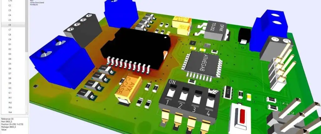
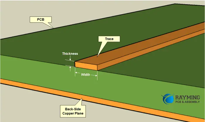
A PCB trace connects electrical signal from one junction to another. This junction can be a componentโ€™s pin, a branch off a plane or a test-point designed for probing. The PCB trace width is crucial when designing a circuit board. PCB designers need to determine an appropriate width for their circuit in order to save it from damage as a result of an increase in temperature.

Traces on a PCB have the capability to handle the greatest current load before any failure. When a higher amount of current passes through a path, heat is usually generated. However, the trace will damage the PCB laminate when the current load passes the maximum limit. This can result in a permanent damage of the circuit board.

Traces are believed to be wires that link several components without any resistance. However, this isnโ€™t a fact as all paths on a circuit feature a particular resistance, which gives a crucial consideration when determining the PCB trace width.

It is important to determine the current carrying capacity and resistance to know the appropriate width to make use of. There are several factors that determine PCB trace width. One of which is the increase of temperature applicable to a circuit board. Temperature increase indicates the traceโ€™s hotness when current passes through it. PCB trace widths are usually measured in thousands of an inch or mils.

What is a PCB Trace Width Calculator?

Diagrammatic Representation of Copper Trace

A PCB trace width calculator helps in determining a PCB conductorโ€™s width or trace. This calculator makes use of programmed formulas. Since trace width is a crucial parameter in a circuit board design, it is important to make accurate calculations. Trace width is crucial for passing currents via PCBs while maintaining trace temperature below a particular input value in order to prevent any form of overheating.

A PCB trace width calculator can help you determine different trace components like voltage drop, trace temperature, power dissipation, maximum current, and resistance. You can determine the trace width according to ampere capacity when using the trace width calculator.

Therefore, you have to determine the design specifications in the calculators like the total length of the path, the greatest current in amperage that passes through the trace, and more. After the specifications have been provided, the PCB trace width calculator will generate a calculated trace width.

Trace width calculator determines the minimum width that will match the specifications you provided. The calculated trace width will enable the flow of current without any damage to the circuit board. In reality, internal layers have more extensive trace width than external layers. This is because the internal layers generate more heat compared to the external layers.

Therefore, it is advisable to integrate the internal tracesโ€™ width for the whole circuit board to ensure safety.

How is PCB Trace Width Calculated?

The PCB trace width is usually calculated using a formula. You need to get familiar with some formulas to get started with this process.

Maximum current

To determine the maximum current, you need to use this formula. A= (T x W x 1.378 [mils/oz/ft2]).

Where A is the cross section area, [mils 2] T is the trace thickness, and [oz/ft2] W is the Trace width.

Trace temperature

The trace temperature helps you calculate the trace width. Trace temperature is determined by using this formula T TEMP = T RISE + T AMB. Three parameters help to determine trace temperature. While T TEMP refers to trace temperature, T RISE is the maximum desired temperature rise and T AMB is the ambient temperature

Resistance calculations

Trace resistance is R= ฯ * L / Aโ€™) * (1 + ฮฑ * (TTEMP โ€“ 25 ยฐC)).

Voltage drop calculation

Voltage drop describes the drop in electrical potential as it passes through a current in a circuit. You can determine voltage drop using this formula V DROP = I * R. I refer to the maximum current while R is the trace resistance.

Power dissipation calculations

When the heat produce by an electrical device causes energy loss, there is power dissipation. You can determine power loss by using this formula P LOSS = R * I2

R Refers to resistance while I is maximum current.

PCB Calculator Trace Width Applications

FULL PCB MANUFACTURING Quote

The PCB calculator trace width is crucial for PCB design process. This calculator can help you determine the tracesโ€™ minimum width while passing the required current. Also, the PCB calculator trace width will need your design parameters to determine the required width. Therefore, you will need to provide values for the rise in temperature, trace length, the trace thickness, and current to pass in amperes.

Furthermore, this calculator will offer the necessary results needed for the external trace layers and internal trace layer in the air. Also, these values are applicable to your circuit board design to confirm the functionality of the board.

Also, PCB calculator trace width helps in determining the lowest trace width for power trace and power signal applications. However, the PCB traces transmit calls that make use of small amounts of current. Therefore, you need to consider other PCB parameters to determine the width.

Types of PCB Calculator Trace Width Based on Industry Standards

There are different calculators for determining trace width. All of these calculators function according to industry standards. There are industry standards guiding their calculations. In industrial and commercial applications, the most common standards are the IPC 2152 and IPC 2221.

IPC 2221 PCB Calculator trace width

The IPC 2221 calculator integrates an equation and a single graph to determine the track current. The equation is I=kฮ”TbAc

In this equation, the value of K is 0.0048 for the visible traces while the value of K for the internal traces is 0.024. ฮ”T indicates temperature change measured in Celsius. The value of B is 0.44 and the value of C is 0.725. A in this equation indicates the cross-sectional area.

To determine the trace width with an IPC 2221 calculator, you can integrate only a range of values. The current ranges between 0 and 35 amperes, the track width ranges from 0 to 10.16mm, the copper width ranges from 0.5 to 3 oz, and the temperature rise ranges between 10oC and 100oC. The results wonโ€™t be accurate if you fail to use these values.

IPC 2152 PCB Calculator trace width

This PCB calculator trace width uses a more recent standard for its calculation. The IPC 2152 calculator is more accurate in calculating the maximum trace current capacity via an improved technical approach. The equation used by this calculator is not as simple as that of the IPC 2221 calculator. The IPC 2152 calculator must integrate a Universal chart to know the unadjusted cross-sectional area.

Therefore, this calculator makes use of various parameters to get a series of modifiers. These parameters include the PCB thermal conductivity, the distance between the copper plane and the passing tracks, and the currentโ€™s thickness passing trace.

Guidelines for Calculating PCB Trace Width

Your design specifications and the current that passes via the tracks will determine your PCB trace width. However, there is a rule of thumb to follow for the applications. 10 mm/A is the minimum trace route to apply. This is applicable for a copper thickness of 1.0 oz/ft2.

PCB trace width is more complex to calculate. Therefore, you need to understand some rules when calculating your PCB trace width. The circuit can work on a maximum current, i.e the trace thickness, the ambient temperature, and the unit of the measurement traces. These will determine the widthโ€™s input ranges.

When you input these figures into the trace width calculator, you will get some output figures. The figures you get is the trace width. You can view all the input information on the PCB datasheet or on the physical PCB. You shouldnโ€™t have any guesswork in this case. Any given PCB should contain this information.

The calculator wonโ€™t allow any calculations to be performed if you fail to input the exact measurements and numbers. You may need to use a magnifying glass to view the input information since circuit boards are usually tiny.

How to Ensure Efficient PCB Trace Width

Minimum width/Spacing

Determine the standard track width

You should determine or know the size of your standard track you will be using within the design. Your circuit will likely experience shorting if the standard track is too close or too narrow. There can be restrictions on the number of tracks in a particular area if the tracks are far apart. In this case, you may have to integrate additional planes in the circuit boards to be sure the circuit board can be routed.

Determine the circuit pad shapes

Component libraries usually feature libraries for PCB footprints and schematic for various components. However, these depend on the manufacturing process. You need to determine the manufacturing process before starting the design. Therefore, you can easily select the optimum pad sizes and then integrate it on the PCB CAD system.

Evaluate the track size for lines carrying current

PCBs have thin tracks which can carry a limited current. Therefore, you need to consider the trace size for any track that transmits power rails instead of low level signals.

Determine the dimensions of the hole and pad

It is crucial to determine the dimensions of the hole and the pad once you commence the PCB design. In most cases, the pad to hole ratio is 1:8. Sometimes, a pad that is larger than the hole can be used to measure. The PCB manufacturer can give you the required standards for their own process. As the holes and padsโ€™ size decreases, the ratio becomes very crucial.

What to Consider when Deciding PCB Trace Width and Spacing Values

PCB trace widths can impact the performance of a circuit board in several ways. There are factors to consider when deciding PCB trace width value.

Signal integrity and electrical performance

Most digital routing on PCBs already have default value for their trace widths, however, some nets need various sizes. For example, controlled impedance nets require the calculation of their trace widths according to the PCB layer stackupโ€™s consideration.

Sometimes, analog routing may need unique trace widths based on the applications of the circuitry. In some scenarios, you may reduce the default trace width in tight areas. However, you need to ensure it doesnโ€™t extend across the printed circuit board.

PCB fabrication

A PCB trace is easier to fabricate if the trace is wider. The etching process has a much better effect on long and isolated traces. Therefore, it is advisable to make the traces wider. For instance, a 20 mil trace will offer better tolerance compared to a 3 mil trace. Also, the copper weight determines the trace widths.

Power and grounding routing

Traces used for power and ground routing must be wide enough to conduct higher amounts of current. Traces can get really hot and burn through if they are very thin. Also, power traces on the PCBโ€™s internal layers should be wider to ensure heat dispersal. Power traces routed on the external layers donโ€™t need to be too wide since exposure to air can help to cool off.

Traces integrated in power supply circuitry should be kept short and wide enough to handle the current. Ensure the spacing for traces carrying greater amount of current is more.

Conclusion

A PCB trace calculator can help you determine different trace components like voltage drop, trace temperature, power dissipation, maximum current, and resistance. You can determine the trace width according to ampere capacity when using the trace width calculator. We provided information about PCB trace width calculator and we hope this information helps you in determining your PCB trace width.

A Closer Look at Flexible Substrates and Their Significance

flexible pcb circuit board

Technology today comprises complex internal components that facilitate the transmission of numerous signals among the user’s inputs & the system’s Storage. With the development of smaller & more manufacturers, advanced devices need elements that can withstand the stresses and demands of various conditions and applications.

In earlier decades, technology was constrained by inflexible internal parts that could clasp under high Degrees of tension. In environments with excessive heat and vibration, any device containing PCBs would quickly fail. Nevertheless, technology has made significant progress recently, thanks to the advent of flexible laminates.

What is Flexible Substrate?

A flexible laminate is a thin, heat-resistant material, typically composed of polymers such as polyimide & polyethylene terephthalate. In modern computing or electronic gadgets, the miniature PCBs that convey signals among the control prompts & screens are frequently fabricated using flexible substrates.

Manufacturers have progressively adopted flexible substrates for printed circuit boards because of their pliable characteristic, which facilitates their insertion into narrow and tight spaces. Additionally, PET laminate can endure the temperatures and stresses of a broad working environment while offering average frequencies with low components.

Major Uses of Flexible Substrate 

flexible-circuit-board-manufacturers

The versatility of flexible laminate materials has led to their application in numerous industries, including the industrial and medical sectors, for various technologies and uses. The Adaptability and robustness of the substance make it ideal for compact devices and challenging working environments. Here, factors such as vibration and extreme heat are commonplace. Here are the principal benefits of flexible substrates:

ยท Automobile Features

As modern vehicles rely more on technology, they increasingly adopt flexible substrates in the car industry. With the emergence of cars, automakers require methods of integrating diverse smart elements into a car structure without adding weight to vehicle design.

Flexible substrates enable automakers to equip modern vehicles with Wi-Fi connectivity, sensing capabilities, and voice commands. Additionally, due to the affordability of flexible components, automakers can add these features at reasonable prices. Furthermore, flexible laminates can withstand the diverse vibrations and tremors associated with the bumps & rough terrain found on the country’s open roads.

ยท Electronics

The current trend toward devices has led manufacturers to produce electronic and computing gadgets that are smaller than ever before. This advancement has been made Achievable by PCBs that can be inserted into small gadgets that can fit comfortably in the palm. Thin, light devices such as smartphones, tablets, miniature video recorders, and digital cameras use flexible substrate PCBs.

ยท Microwaves

Devices that create high temperatures require components that can withstand extreme heat levels while remaining flexible and durable. Consequently, flexible laminates have become essential in the functioning of ovens. Every time you heat a cup of coffee in under 60 seconds, a series of processes are facilitated by substrate PCBs. It sends a message from the button you press to start the microwave, which makes the microwave produce heat and warm up your food or drink.

ยท Industrial Applications

Machines that operate along conveyor belts in factories & processing plants experience a significant magnitude of anxiety throughout the workday. Previously, these devices depended mainly on electricity & compressed air energy since PCBs were too sensitive and cumbersome for the rigors of the industrial environment. However, due to the robustness and thermal resistance of substrates, computing technology can now be integrated into industrial machines, allowing them to carry out a wide variety.

 Of Intensive procedures.

ยท LED Lighting

Flexible substrate PCBs have addressed the concern of heat generation in LED lighting systems, which has been one of the main issues associated with this lighting technology. Despite competition from other lights, LED lighting has gained popularity due to its energy-saving and efficient features. Using flexible substrate printed circuit boards has eliminated the wastage of energy and temperature impacts on working environments.

ยท Medical Devices and Implants

Because of their miniature size and pliable characteristics, PCBs fabricated with this ultra-thin substrate have become a crucial component in modern medical devices. Flexible substrates(laminates) are now utilized in a wide range of applications, ranging from surgical instruments to electronic Embeds.

ยท Power Electronics

Flexible substrates, when Joined with thin layers(copper), find application in the power electronics industry. They are particularly important for high-power devices that require stress-resistant durability to operate at maximum capacity.

Use of Flexible Substrate in Printed Circuit Boards 

FULL PCB MANUFACTURING Quote

Multi-layered circuit boards containing integrated circuits, interfaces, and microchips can be fabricated using flexible substrates. These circuit boards have a similar appearance to modern PCBs that are simple, sleek, and unencumbered. However, the key difference is their flexibility and ability to bend significantly without compromising functionality.

Flexible substrate PCBs require a less array of elements compared to traditional PCBs. Despite its compact size, this equipment can achieve high-density functionality with just a Minimal amount of surface area. As a result, flexible substrate printed circuit boards are good for small equipment that needs high-performance capabilities for multiple functions.

The flexibility of substrates makes them an ideal choice for PCBs, as they can withstand vibrations, tremors, and high temperatures without compromising their functionality. Despite these stress factors, flexible substrate printed circuit boards maintain their high-performance capabilities. This makes them particularly useful in challenging environments such as factories and power facilities, where they can deliver average signal integrity.

Flexible substrate PCBs operate with minimal mistakes as they lack wiring components and mechanical connectors, which can introduce errors. Additionally, their assembly methods are relatively uniform, making them compatible with various devices. Flexible substrates enhance the reliability, robustness, and high-performance capabilities of PCBs, which is why modern manufacturers increasingly prefer them over rigid PCBs.

Amazing Advantages of Flexible Substrate

Bendable materials provide significant advantages to printed circuit board manufacturers & the businesses or organizations that utilize them in their Advanced computational systems. The flexibility of substrates makes the boards easier to uninstall, install, handle, and repair, reducing their overall complexity. Additionally, flexible substrate components are cost-effective and easier to manufacture than rigid PCBs. Overall, the Advantages of Flexible materials can be summed up as follows:

1. Reducing Weight and Space

Flexible substrates are easier to integrate into a wide range of Digital devices due to their reduced size and weight. They can be Set up in even the smallest computing equipment available today. The light weightiness of flexible substrates makes them ideal for motherboards for laptops & all-in-one devices. Printed circuit boards made of flexible substrates can significantly reduce space volume by up to 50% and decrease weight by 90 percent making them highly advantageous for many applications.

Flexible laminates are particularly well-suited for use in the aerospace & medical industries. In hospital equipment, the lightweight nature of flexible substrates enables the construction of more compact yet intricate devices that can be easily moved from one room to another. Similarly, the lightweight and compact characteristics of flexible substrates make them the ideal choice for devices used in air travel.

2. Easier Installation and Service

Flexible substrates can be easily installed by flexing and bending them into a printed circuit board. This flexibility greatly reduces the difficulty and labor of assembling some of the smallest boards and devices. As a result, using flexible substrates generally results in lower manufacturing costs. Additionally, maintenance and servicing devices with flexible laminate components are easier, as the material can be easily manipulated for repairs and modifications.

3. Increasing Reliability

Flexible laminates are more reliable than earlier altered markets due to their minimal interface connections. With a flexible substrate, there is less reliance on connectors, solder joints, solder, and other interface components, reducing the possibility of failure. Additionally, flexible substrates possess the strength to withstand the impacts of vibrations, heat, and shocks, making them suitable for boards used in devices designed to cope with high temperatures and turbulence. As a result, devices with Bendable bases

 are generally robust enough to withstand even the most grueling military & medical applications.

4. Managing Heat

Flexible substrates offer exceptional heat resistance and flexibility compared to other options, making them suitable for device components that face higher temperatures in humid environments. And industrial These substrates can resist temperature changes that cause other materials to expand and contract over time. Additionally, flexible substrates are largely resistant to the effects of gas, oil, acid, UV exposure, and radiation. This makes them a reliable choice for devices used in harsh environments, such as in the military and medical fields.

5. Improving Aesthetics

The transparent look of flexible substrates not only enhances the aesthetic appeal of electronic & computing devices but also makes it easier to identify the internal parts. In the past, internal parts of electronic components were often hidden behind wires & elements, making it difficult for non-experts to identify them.

With flexible laminates, the internal parts of newer components are more visible, making them less intimidating for the optimal user. In industrial settings, IT personnel and computing staff can quickly identify flexible laminate parts since wires and other through-hole elements don’t protect them.

6. Eliminating Connectors

Flexible substrates eliminate the need for interface connections in electronic and computing components. They can also accommodate most elements if they apply to rigid printed circuit board design. PCBs with flexible substrates are flat or sleek in Look

As a result, they can be easily put in slots in small devices because of the absence of Intricate interconnects

7. Reducing Assembly Costs

Flexible substrates’ thin and lightweight nature makes them easy to use in tight spaces, which reduces the overhead costs associated with manufacturing components. Additionally, using flexible components substrates can lower packaging and material costs.

Future of Flexible Substrate in Electronics Industry 

Shortly, flexible substrates witness a surge in their application across various fields, such as electronic memory. PET substrates, which offer both durability and flexibility, will likely drive further technological progress in light control, memory storage, and signal transfer within the computing and electronics industries.

Using flexible substrates in PCBs for computing equipment can significantly advance memory storage for small devices. It is possible that in the future, manufacturers could produce thumb-sized equipment with the capability to store high-quality movies & run many programs simultaneously, all through the use of voice commands. These tools could be Suitable with large screens that display high-resolution, full-color images and come equipped with integrated speakers. The control of these features is manageable remotely through voice-activated Artificial Intelligence technology. It is all possible due to the implementation of substrate-printed circuit boards.

Using PET flexible substrates drives progress in the smart car industry. With the increasing likelihood of driverless cars dominating the roads shortly, flexible printed circuit boards will play a critical role in enabling high memory capacity, advanced sensing technologies, artificial intelligence, or remote connectivity in these vehicles. Moreover, Similar technology is leveraged in airborne power vehicles. It is potentially reducing reliance on conventional transportation infrastructure such as bridges and roads.

Bendable base materials will likely be crucial in developing futuristic technologies such as robot maids and delivery drones. With a decreasing reliance on cars and expanding businesses through the Internet, clients can order food and clothing from far-off restaurants and shops through drones. These flying robots may rely on flexible circuit boards that have a large capacity, can handle stress well, and are long-lasting.

Flexible Substrates from RayPCB

More and more manufacturers are realizing the advantages of flexible laminates and are switching to them as an Element for PCBs. With flexible printed circuit boards, even the tiniest devices are furnishable with greater power and durability than The bigger versions. We offer a variety of flexible boards. Contact us today to learn how flexible substrate-printed circuit boards can help your devices perform better. We’ll be happy to share all the details with you.

Everything You Need to Know About Thermal Clad PCB

Thermal Clad PCB

The demand for higher power output in today’s electronics industry often leads to increased heat generation, which shortens the lifespan of circuits. RayPCB has tackled this issue by utilizing materials other than the standard FR4 for circuit building.

RayPCB provides thermal clad on aluminum, which functions as the thermal sink by thermal dissipation & enhancing overall circuit strength and durability. Manufacturing circuits on these substrates has been proven to reduce core temperatures and COE.

Contact us to have your printed circuit designed or built on the heat-clad substrate. This will not only provide upgraded performance but also help prevent field failure in your circuit boards.

YouTube video

Benefits of Thermal Clad PCB

ยท Thermal Conductivity

Meeting today’s high-speed PCB requirements often requires materials with low Dk and low loss properties, but these materials may not have the necessary thermal properties to optimize their performance. In the past, adding copper weight to multilayer PCBs was a common solution, but this significantly increased the cost and introduced multiple Mechanical connectors among layers that could fail over time.

Metal core boards offer a better alternative by minimizing the no. of interconnects required and providing many PTH opportunities for clients to link with the inner metal core, ensuring even heat dissipation.

ยท Thermal Stability

Designers face a major challenge when Advancing technology that involves multiple materials – ensuring they consider the unique Attributes of all materials, particularly in terms of thermal compatibility. For PCBs, the crucial variable is the CTE of each material. Matching substances with the right Z-Axis Thermal expansion coefficient values is crucial to minimize material expansion during operation, which can lead to delamination separation in metal substrate PCB.

ยท Overall PCB Rigidity

For numerous printed circuit board applications, the Capability to withstand shock or vibration is crucial for ensuring the long-term Stability of the end product. By incorporating copper, even carbon composites, and aluminum, we can significantly increase the rigidity of the PCB. These materials Enable us to create PCBs that are two -four times Harder than standard FR-4 and polyimide designs.

Major Challenges of Thermal Clad PCB

fr4 thermal conductivity

Below are some major challenges fabricators typically encounter when producing metal-core printed circuit boards. These issues have been consistently documented over many years of experience and can significantly impact the efficiency and cost-effectiveness of MCPCB production.

ยท Plated Through Holes

Preparing the hole wall is a major challenge in creating metal-core circuit boards (and any type of PCBs, for that matter). It is important to clean out all the debris from hole drilling so that a dependable and strong hole can be created.

Traditional de-smear Approaches or processes are ineffective in this situation. Therefore, it is crucial to utilize plasma etching for these boards. Additionally, it’s essential to have a Control sample on the development panel that is cross-sectioned to verify the cleanliness of the hole wall before electroless copper deposition (the only suitable Technique of depositing metal for this application) because there is no going back.

ยท Similar Thermal Expansion Properties

As previously mentioned, understanding the operating CTE temperatures is essential for the reliable function of metal-supported PCBs. However, it’s just as crucial for the manufacturer to comprehend the thermal expansion parameters when producing processes such as HASL and lamination cycles. Thieving is often deliberately incorporated into production panels to dissipate heat from the components.

ยท Extremely Tight Tolerances

Conventional PCB tolerances of +/- 0.005โ€ or +/- 10% for mechanical & electrical properties could be inapplicable to MCPCBs. When attempting to combine high-speed functionality with the metal core printed circuit board, tight tolerances of +/- 0.001โ€ may be necessary. Achieving these tight tolerances often requires precision CNC machining for routing to & through Metallic cores, especially for the Mechanical features.

ยท Heat Sink PCB

In the past, before the technology to Apply metal elements as a Printed circuit board center was available, the most economical approach was to manufacture a Detached metallic thermal sink. The finished PCB would be inscribed to the heat sink and attached using liquid adhesive or conventional pre-preg in the heating equipment under pressure and heat.

Importance of the Dielectric in Thermal Clad PCB

The dielectric material is significant in a metal-clad printed circuit board as it is the primary factor distinguishing the base materials used in their production. Additionally, the thermal Characteristics of the substrate are influenced by the dielectric layer, and it is also the fundamental layer that Specifies the Total dependability of the Finalized PCB.

Various materials are employed in the creation of dielectrics, including:

  • polymer
  • Ceramic
  • Boron Nitride
  • A combination of the materials above
  • Epoxy

Low thermal impedance is a fundamental thermal property required in a thermal substrate. For this reason, PCB manufacturers require dielectric materials with excellent thermal conductivity. To achieve Low thermal insurance, a thin layer of dielectric over the aluminum base is preferred. However, making the dielectric layer too thin is not recommended, as this can lead to a lower dielectric strength of the laminate.

Thermal Properties of Clad PCB

FULL PCB MANUFACTURING Quote

The thermal properties of a metal-clad printed circuit board are noteworthy and are below:

ยท Thermal resistance

This property determines the conductivity and thickness of a metal-clad printed circuit board. The material’s thickness or surface area can affect the thermal resistance value.

ยท Thermal impedance

Thermal impedance refers to a Material’s capability to resist heat flow, and from a printed circuit board standpoint, this value should be as low as possible. Lower thermal impedance facilitates Enhanced heat dissipation through the PCB and towards the Thermal sink.

The heat conductivity of a material directly affects the thermal impedance value. Hence, it is an intrinsic property, and its value varies with the thickness of the material.

ยท Thermal conductivity

It is the measure of a substrate’s capacity to conduct heat, and it is in W/mK. As a substance property, the heat conductivity remains constant irrespective of the material’s dimensions. For example, the heat conductivity of ten centimeters of gold is equivalent to 100m of gold.

Factors to Consider While Designing Thermal Clad PCB Boards

When designing a printed circuit board, numerous factors should be considered. It is essential to create a design suitable for the intended Intention of the end product. At the same time, the layout should also be Efficient to minimize its impact on the overall rates of the printed circuit board.

ยท Material selection

A metal-clad printed circuit board technology is on eliminating heat from the End product, which enhances its lifespan. Consequently, it is crucial to consider the specific requirements that the material must fulfill. Certain materials are better for particular applications and meet the necessary specifications.

ยท PCB size and shape

Base materials for PCBs are available in various sizes, emphasizing the significance of the design’s shape and size. Rectangular or square shapes are preferable because of the tessellation, which increases their yield.

In fabrication, square or rectangular shapes are the most commonly useful process, making them suitable for high or low-volume production. Moreover, they offer optimal yield for every creation panel, as no additional spacing is essential between PCBs.

ยท Surface finish

The choice of Surface appearance should be based on the intended application of the final product. Additionally, the surface finish used for populating the boards during assembly will play a crucial role. Each surface finish type has unique advantages and disadvantages, to determine if it satisfies the application requirements.

Conclusion

Thermal-clad printed circuit boards have gained widespread popularity across various applications, particularly with the increasing demand for LED lighting. These boards are particularly suitable for high-current applications and offer more advantages than FR4 circuits.

Exploring the Basics of X-Ray Tube Filament Circuits

filament circuit

As the source of X-ray radiation, X-ray tubes are also referred to as the X-ray device’s “engine.” The tube X-ray does, however, include other internal parts that it employs to produce X-ray radiation. The filament is arguably the most crucial of these parts since it works in conjunction with the X-ray tube’s other internal parts to generate the necessary electron beam. Knowing how the filament works may be quite useful, especially when determining how much voltage and amperage to provide the filament throughout the operation of the X-ray machine.

So let’s get started if you want to learn everything regarding the filament.

YouTube video

What Is The Filament Circuits Of An X-Ray Tube?

The filament often forms a crucial component of a cathode. It is in charge of releasing the circuit’s beams of electrons so they may focus on the target of the anode. The filament, which is simply a wires coil, serves as a controlled supply of electrons for the X-ray beams that are produced when the filament is heated. A cup-shaped nickel creation that is utilized to concentrate the beams of electrons onto the anode is also where a filament is situated. 

What Is A Filament Circuit?

The filament PCB, a subcircuit of the basic X-ray device circuit, is in charge of delivering a relatively low current to heat the filament and liberate electrons from it. Inside the tube X-ray, thermionic emission is used to liberate the electrons. The operator must use the generator’s amperage selector to turn on this circuit. This is split into two sections via a step-down generator. Additionally, the filament circuit’s amperage is controlled by the current chooser. This is also in charge of controlling the heat produced when the X-ray device is in use.

What Is Filament Circuits Current In An X-Ray Tube?

The current of the filament is the electrical voltage that excites the filament and causes it to generate electrons. The heat produced when this current travels across the filament typically reach a point where few electrons are released from the forces of electrostatic attraction holding them inside the filament. Naturally, the number of free electrons inside the filament is frequently inversely correlated with the current running through it. While not exactly the same, it is roughly comparable to the amperage that the X-ray device operator controls. 

Material of The Filament Circuits

The components of the X-ray tube, which also include filament, are built from substances that can survive the tremendous heat energy generated during X-ray processing. As a result, tungsten is used to create the filament because of its excellent temperature resistance and suitability as a filament material. However, the tube X-ray often has a cooling mechanism to lessen the impact of the temperature. Nevertheless, the filament and the X-ray tube’s lifespan may get short if the tungsten substance begins to melt when the process of cooling is insufficient for sustained heat.

Despite the fact that the filament serves as a part of the X-ray tube, it is specifically situated inside another structural part, the focusing container or cup. Without this focusing cup, there is a risk of greater electron scatter. This renders the electron projection inefficient and may overheat the filament, causing the tungsten substance to evaporate.

Maximize The Life Of The X-Ray Tube Filament Circuits

Every X-ray device must produce electrons to function, and this process causes the filament to generate heat. Tungsten emits electrons in large quantities at temperatures of about 2,000 ยฐC. 

The use of low voltages for powering the filament for as long as feasible is a useful preventative maintenance technique to extend the lifespan of the X-ray tube filament. Continuously applying a high voltage to a filament shortens its lifespan by causing the filament to thin down over time.ย 

Utilizing the chart of the manufacturer is another smart move to prolong the life of the filament. Manufacturers of X-ray tubes frequently offer graphs and charts that illustrate the ideal settings for variables, including amperage, startup time, exposure duration, and voltage needs. Through the use of these combinations of settings, you may extend the life of the filament in the X-ray tube.

Similarly, ensuring that the cooling mechanism operates at peak efficiency will lengthen the lifespan of the filament in the X-ray tube. Heat may result from a malfunctioning cooling system.

Why Filament Circuits X-Ray Machines Are Becoming Popular In Electronics Industry? 

FULL PCB MANUFACTURING Quote

Over the previous few decades, electronics production has constantly advanced, with advancements in the communication, industrial, aerospace, and military sectors making inspection much more challenging. The following are some most notable trends that have a detrimental impact on inspection:

ยท Component Placement

In order to maximize functionality and conserve space, equipment is getting more compact. Thus, many solder connections and components in electronics are being shifted to interior layers, either between Circuit layers or concealed within the finished device itself.

ยท Compact Size

The trend toward miniaturization is increasing among PCB components. PCB electronic components are anticipated to continue moving in this direction due to the requirement to make increasingly thick boards.

ยท SMT

The surface-Mount approach creates smaller packages and leads. This results in a higher PCB density along with hidden components between layers.

Traditional inspection techniques are almost completely unable to adequately discover flaws in Circuits and their electronic components. This is because of their increased density, shrinking size, and complicated arrangement. The dense quality of contemporary PCBs makes optical, ultrasonic, and thermal imaging techniques comparatively useless.

X-ray inspection, on the other hand, has the capacity to acquire precise pictures that these other techniques lack. X-ray is more advantageous for evaluating solder connections on intricate PCB assemblies since it can penetrate through PCB layers to examine interior packaging and layers. This is why the technology of X-ray is more and more useful for PCB examination.

Working of Filament Circuits X-Ray Inspection 

You must first understand the principles of X-ray inspection in order to comprehend what does an X-ray Circuit Board inspection mean? Three components serve as the basis for all X-ray examination devices:

ยท X-Ray Tube

This tube possesses the capability to produce X-Rays photons.

ยท Platform 

The sample goes through examination from a variety of angles and distances thanks to the operating platform’s ability to move it in various different directions.

ยท Detector

The detector over the sample’s other side collects and catches the X-ray photons and converts them into a visual picture or image.

X-ray photons are transmittable through an object. Depending on a material’s physical characteristics, which include atomic weight, thickness, and density, x-ray photons travel through it in different ways.

In general, heavier materials are simpler to photograph because they absorb relatively greater X-ray photons. At the same time, lighter elements tend to be more transparent. The number of photons that are together on the opposite aspect of the item depends on how each substance reacts differently, producing a picture. Typically made of heavy materials, PCB components are simple to spot on an X-ray picture.

Advantages Of Quality Filament Circuits Control And Inspection

Metal appears black in X-ray pictures of PCBs, but plastic, ceramics, and glass are translucent. This makes metallic components visible. With magnification features, this enables inspectors using X-ray equipment to check PCBs to view different metallic components on a PCB. Inspectors will be able to observe a PCB’s many characteristics. Also, see a variety of possible issues thanks to the x-ray, including:

1. Solder Bridges

The Solder bridges of PCBs are a prevalent issue. This typically happens when a solder joint gets too close or makes unwanted connections. Typically, other electronic components hide these solder issues. This makes it challenging to detect them visually, but X-rays may quickly find them.

2. Solder Voids

As an outcome of water contaminating solder paste, solder voids develop when flux or gas becomes trapped while soldering. These voids can result in physical flaws and decreased dependability. They also limit thermal conduction at a solder connection. To assure the quality of the product and the manufacturing process, it is crucial to employ X-rays often. This proves one of a few ways to detect solder vacancies.

3. Pin-Hole Fills

Circuit boards frequently have issues with through-hole connection pin-hole fill that is insufficient. These flaws are utilizing X-ray equipment, which can also be useful to calculate the quantity of fill that is missing utilizing coordinate measurements.

Conclusion

Even though the filament of an X-ray tube is a crucial component of any X-ray machine, being aware of how it functions may be quite advantageous. It not only generates the electrons needed for the X-ray device. But also makes sure that the amount of radiation required for a precise examination of the sample is created. Moreover, to make sure you optimize the life of the tube filament of the X-ray, maintenance and care best practices must be used. 

The Essential Guide to Electronic Component Packaging

QFP vs QFN Packages

Optimizing SMD (surface mount device) packaging is essential for efficient assembly production and should be tailored to the SMT machine’s feeder types and quantities. There are four primary packaging options for SMD components, including tape, bulk, tray, and tube. For large-scale production, it’s best to use Tape Packaging. However, everyone recommends, for prototype or low-volume production, anti-static integrated circuit tube packaging. You cannot use Bulk packaging since it requires individual pickup or equipment for re-packaging.

Electronics demand meticulous attention to packaging. They are not only expensive and delicate but also susceptible to ESD. Hence, it is crucial to use protective packaging to safeguard against mechanical and physical damage during transportation.

In this article, we will cover all the essential information about packaging for electronics.

YouTube video

Importance of Electronic Component Packaging

Considering the factors above, it is evident that the electronic manufacturing industry. Faces significant challenges. Due to their fragility and high cost, any harm to electronics during transport can have severe consequences for both the financial standing and reputation of a business.

Static charges can also cause damage that may not be immediately noticeable. If a product does not power on, is not functioning right, or has a shorter lifespan than expected, it is likely that the packaging solution is to blame.

Hence, to achieve a successful packaging solution, it is necessary to ensure protection against effects during transit, moisture, mishandling, dust & static charges.

Types of Electronic Component Packaging

1. Tape packaging

It is the most famous packaging form for electronic components. It is adaptable, efficient, and has been regularized. You can use this packaging form for all IC components except PLCC, QFP, & LCCC. Three kinds of tape are present in this packaging: plastic bag, paper tape & Surface mount tape. You can use this tape for packaging chip resistors and capacitors. Plastic bags are utilized for packaging several chip leadless elements, composite elements, special-shaped elements, SOP, SOT, Thin QFP, & other chip elements. You can use Carrier tape and reel packaging resistors, diodes, capacitors, transistors, Small ICs, crystal oscillators, and other patch components.

2. IC Tube packaging

You can use it for rectangular chip capacitors, resistors, small devices, and certain special-shaped components. It is ideal for situations with multiple SMT electronic elements in small batches. During packaging, manage the aspects in one direction & place them into the plastic tube. Next, insert stoppers such as plastic pins, nails, or rubber end plugs at all ends of a line & remove the cover of the SMT box. Then, following the mounting process, a chip element is fed to the substrate when the tube presses.

Tube packaging may have a higher cost for materials, and it may not be able to accommodate a large number of electronic components. Additionally, there is a risk of trapping elements in a confined space if the pressure is not evenly distributed. However, for SM integrated circuits, tube packaging is less expensive than tray packaging. However, it isn’t fast like the Carrier Tape packaging.

3. Tray packaging

Tray packaging divides a tray into the same parts using rectangular partitions according to cavities. It also places components individually into each hole, with an average of fifty pieces/tray. Once one is installed, then cover the tray with a protective film. There are Thermoformed Trays with single-layer, ten-layer, three-layer, twenty-layer, and twelve-four-layer tray feeders available. This method was initially applicable for high, medium & multilayer capacitors with larger shapes. Still, you can also use them for packaging elements such as QTP and SOP with many pins.

Tray packaging has two types: floppy trays and hard trays. You can use hard trays for packaging multi-pin and QTP components to prevent the wires from deforming. On the other hand, you can use Floppy trays for packaging common special-shaped elements.

4. In bulk

Bulk packaging encloses chip elements in the plastic box/bag without any particular arrangement. During mounting, one inserts a plastic box into a substance rack, and the components are fed into an SMT machine material port using the feeding tube. This method has a low cost and small size but a limited application scope. 

Functions of Electronic Component Packaging

Electronic packaging design involves the integration of multiple small packages that work together to achieve a desired purpose. The packaging safeguards the printed circuit board & electronic elements from external damage. It also ensures that they do not interfere with the functioning of these elements. Nowadays, everyone views unpacking as expertise.

Packaging organizations (electronic) are under significant pressure due to the rapid evolution of electronic packaging design functions driven by technological advancements. As technology continues to improve, the demands on electronic packaging also increase and change accordingly. So it leaves these companies with the challenge of keeping up.

Two factors primarily derive from Electronics packaging: the rapid evolution of silicon IC (integrated circuit) technology and the continuous development of photonics. It is incorporated into different levels of interconnections for bespoke electronic packaging. It requires electronic packaging strategies to constantly adapt & modify their functions to keep up with the changing landscape of technology.

When it comes to photonic technologies, physically attaching these electronic elements to the printed circuit board raises the design to an advanced level. However, there is a physical connection between these components with other basic features in the system. It can pressure the schematic layout of packaging (electronic).

Different Tiers of Electronic Component Packaging

FULL PCB MANUFACTURING Quote

Electronics packaging design has several tiers, specifically Level 0 through Level 5.

  • Level 0 โ€“At this tier of electronic packaging, the primary focus is safeguarding the chips & semiconductors, which serve as the fundamental and essential components of the electronic setup.
  • Level 1 โ€“At this level of electronic packaging, the goal is to shield electronic components from damage.
  • Level 2 โ€“ The PCB is safeguarded at this level of electronic packaging.
  • Level 3 โ€“At this level of electronic packaging, the assembly, boards & their related components are shielded and secured.
  • Level 4 โ€“ Modules or groupings of assemblies are safeguarded at this level of electronic packaging.
  • Level 5 โ€“ At this level of electronic packaging, a mixture of various modules and some electronic systems is protected and secured.

These levels enable electronic manufacturing firms to readily identify the necessary electronic packaging substances for a design, streamlining operations and increasing efficiency. By specifying the current electronic packaging tier they are working on, they can quickly locate the required components.

Top tips for Electronic Component Packaging

Ensuring the safety and security of a package must be the topmost priority, particularly when shipping fragile and valuable electronics. To avoid costly damages & returns, consider these simple tips.

  • Properly secure batteries for shipping โ€“ Numerous electronics rely on batteries, either integrated or detachable, for power. If not packed correctly, these elements can pose a significant risk of generating hazardous heat, fire, or sparks during shipping. To prevent such incidents, it is essential to safeguard all battery connectors against short circuits. One can achieve it by covering them with a non-conductive, insulating material.
  • Separate cords and accessories โ€“In instances where electronics comprise multiple components, it is advisable to keep them well-organized within the package. Separating accessories and ropes can be highly beneficial for the user, as it prevents tangling, enables appropriate labeling of each component, and enhances the overall customer experience.
  • Use effective shipping materials โ€“ Choosing the appropriate materials is crucial to ensure your electronics reach immaculate condition. Void fillers, & antistatic products are some options you can use to safeguard your products. You can keep them secure during transportation.
  • Deter and detect damages โ€“ Electronics are susceptible to damage during transit, which can be detrimental to your business due to their fragility and high cost. However, by utilizing impact signals, you can mitigate & detect defects during shipping to prevent losses. ShockWatch labels have an excellent Tamper-evident solution. You can apply it directly to the package. They act as a visual deterrent for package handlers and provide physical proof of impacts between five and seventy-five by releasing red dye. To learn more about impact indicators, refer to this recent case study in which these labels maintain high-tech devices in a new situation.

Challenges for Electronic Component Packaging

If your company deals with the production or shipping of electronic components, then you understand the importance of protecting these elements during storage & transportation. Electronic parts are extremely susceptible to harm caused by oxygen infiltration and other corrosive elements present in the environment.

ยท Packaging Challenges

Selecting the appropriate packaging for electronic components that you can rely on can be a challenging undertaking. Buying unsuitable packaging can result in expensive waste & damage to your organization’s reputation. Therefore, you will undoubtedly want to take all necessary measures to safeguard your enterprise assets.

Moreover, electronic components come in various sizes and shapes that are often irregular, making it challenging to find suitable packaging solutions that can effectively protect them. It is not easy when safeguarding electronic elements & electrostatic discharge, as the appropriate packaging options are more limited.

ยท The Solution

Aluminum laminate foil packaging can protect your electrical elements against corrosion during storage or transportation. Whether an entire machine or a motherboard, this packaging option can safeguard your equipment. But what sets it apart from other packaging materials?

AOI Machine: A Comprehensive Overview of Automatic Optical Inspection Systems

flex pcb manufacturing process aoi

Make sure the PCB or Circuit Board you employ in the projects will function properly and satisfy your customers. It’s critical to possess a reliable method for checking PCBs for faults and making sure they work as intended.

The size and complexity of PCBs are both increasing; today’s PCBs can contain numerous soldered joints with a huge number of microscopic components. Errors may occur more frequently as a result of the increased complexity. Automated optical inspection or AOI approaches can give more clarity and accuracy when a typical visual examination is unable to discover minute flaws in a crowded, tightly packed board.

YouTube video

How Doesย AOI Machineย Work?

How can one define AOI? The Automatic optical inspection involves an electronic scanner that employs light imaging to visually check the finished PCB. It assesses the level of craftsmanship to ensure that the Circuits are appropriate for usage and purchase.

A typical AOI system includes several light sources, numerous cameras, and maybe even video cameras. Several light sources from various perspectives illuminate the Circuit board. Moreover, the cameras click videos and photos to produce a complete image for analysis.

Without the requirement for a manual visual inspection, AOI measurement often employs a scanner to autonomously scan the item. The scanner checks for larger problems that would impair the quality of the PCB as well as tiny errors that might result in catastrophic failures, like the lack of a crucial component. Smaller flaws include things like slightly misaligned parts and soldering that creates the incorrect shape or size.

At several phases of the production process, AOI is helpful. It performs well for the inspection of solder paste, bare PCBs, and pre and post-reflow. Each step has the potential to create design flaws in a PCB, and AOI aids in identifying these flaws before production on a defective board continues.

Although, the majority of AOI happens during post-production. This is because the AOI may employ an individual system to simultaneously examine several types of faults. One thorough inspection takes relatively less duration than one inspection after each stage of the procedure. Utilizing AOI for a final verification allows the production process to move quickly and enables it to meet deadlines and higher productivity. Additionally, the problematic boards also go back for repair while the remaining boards proceed if AOI discovers faults during the post-production phase.

The Role Of AOI Machine

PCB manufacturing depends significantly on AOI. It ensures that every board can deliver the high efficiency needed in intricate electrical devices.

When AOI finds a PCB defect, it marks the PCB and sends it back for rework. This procedure may take place in a number of distinct manners. The results of the AOI may not meet some facility specifications, such as all the PCB lines ought to be larger than a particular size. In this situation, people may examine the results and choose which boards need repair. AOI can make a comparison between the actual PCB and a CAD rendering of an ideal PCB. When the real PCB diverts from the desired design, AOI automatically spots those areas and flags the PCB for reworking.

For PCB manufacture, AOI offers the following advantages:

ยท Ensuring Quality

You may use AOI to verify that the PCB products work as planned. Increasing customer happiness, improving your company’s reputation, and giving clients assurance about the service quality you’re providing all benefit from maintaining the PCB quality.

ยท Evaluating A Complex Board

A board from Millennium Circuits will automatically go through AOI if it has over 100 components. The naked eye is incapable of inspecting complex PCB layouts with the same level of precision as AOI.

ยท Improving Processes

If flaws occur from defective processes, grasp them right away using AOI. AOI may assist you in identifying defect patterns and modifying your procedures before producing thousands of PCBs with the same defect. According to the latest study, finding a flaw in a PCB that has just been assembled is just ten times more expensive than finding one in a bare PCB. Yet finding a flaw in a PCB that has already been put to use in the field is around 1,000 times more expensive. Early mistake detection reduces the possibility of future repair and improves the productivity of your manufacturing processes.

ยท Customizability

Even though AOI operates fully automatically, the operator may still specify the parameters that will inform the scanner where and what to look for. It’s simple to tweak your parameters to locate the defects you need if the design requirements change.

Reviews of AOI Machine

Automated-Optical-Inspection-AOI-Equipment

The following constitute a few of the elements evaluated while an AOI:

Soldering Defects

Soldering employs a very low-melting-temp alloy, frequently lead, lead-free or tin alloy, to bond the PCB’s electrical components. With the exception of not melting the electrical components, the procedure is comparable to welding. When the bonds between two electrical components don’t form properly, this is known as a soldering fault.

The following are some typical soldering flaws that AOI might look for:

ยท Open Circuit

PCB’s open circuits are typically the main problem. The reason is that an incomplete or open circuit stops the current from passing through them. The board won’t operate properly if a circuit is wide open.

Open circuits may arise due to inadequate traces or vias. These improper traces form due to inefficient soldering. An evident open circuit may occasionally be found by eye examination, while AOI can find even marginally open circuit points and mark the PCB for correct circuit closure.

ยท Solder Bridges Or Solder Shorts

Solder bridges happen when two PCB components are connected electrically, even though they shouldn’t be. These bridges may develop if a board is produced with an excessive amount of solder or if solder leaks into a solder-free section of the PCB.

If the solder paste fails to detach from its tips or leads prior to solidifying, solder bridges frequently happen. The metal pads known as leads are used to link two places on a circuit board. Due to the size of the leads, the amount of paste bonding them to a PCB, or the shallow pitch of the PCB, the solder paste may not separate.

Solder bridges cause problems as they hinder the desired current flow through the circuit. They may short-circuit the PCB or destroy vital components or vias. Additionally, solder bridges are extremely hard to spot with the human eye; even minute solder seepage may allow them to develop. Luckily, AOI scanning may detect even the smallest solder bridges or shorts and return the defective circuit boards for correction.

ยท Insufficient Solder

When the manufacturing process utilizes insufficient solder to bind various components onto the circuit, an inadequate solder connection develops. Solder skips happen when the solder occasionally fails to join the components completely.

The PCB’s performance will suffer if the connections of components are improperly soldered because they may not produce solid electrical connections. Additionally, the PCB will have missing parts if there is insufficient solder to hold the electrical components in place, which will very certainly lead to catastrophic failure. If a board has to be resoldered, an AOI may scan it, note how much solder is on each electrical component, or compare it to the right picture.

ยท Excess Solder

When the reverse occurs, that is, when the manufacturing process soldiers the board, excess solder results. Sometimes it happens as a result of using too-wide soldering tips or applying too much heat.

Solder bridges and other defects like excess solder might be problematic. A huge spherical solder ball may form when excessive solder is applied to a board pin during production, making it hard to determine if the board pin is adequately moistened to adhere to the PCB.

Due to their size, solder balls or bridges are generally simple to spot, although a human examiner may skip one after examining hundreds of almost similar boards. With the use of a solder wick or solder sucker, an effective AOI scanner may quickly identify excess solder and return the board for repair.

Component Defects of AOI Machine

Defects in the tiny functional elements connected to a PCB are known as component defects. Here are a few typical PCB component flaws:

ยท Lifted Lead

When one small metal pad on a circuit doesn’t stick correctly, the lifted lead results. Sometimes a raised lead happens as a result of manufacturing handling, extreme heat, or board flexing. On the other hand, it happens when leads that are excessively long rise once they touch solder.

The instability of lifted leads makes them troublesome. Pins may link to a copper sheet below using the metal pads on the PCB. However, if somehow the lead rises, the pins won’t allow it to do so correctly. Missed connections may harm the operation of the board and lead to component failure.

ยท Missing Components

A Circuit board may miss an electrical component due to various causes. Inadequate soldering may result in components going missing, or the manufacturing process may omit a crucial component.

A PCB with a missing electrical component has a major fault that might result in catastrophic failure. The naked eye may see the missing part. Yet, since this is a serious flaw, having a trustworthy AOI scanning device is essential for identifying the missing components in PCBs before they reach end users.

ยท Misaligned & Misplaced Component

 Misplacement or Misalignment can happen when the manufacturing process installs components wrongly or when electrical components move after placement. Due to the ease with which parts can move on top of molten solder due to the solder’s low surface tension, component shifting often occurs during reflow.

The PCB may function even with a misplaced or misaligned component, although it may operate slowly. Or it may not function at all. The ability to detect alignment issues requires a reliable AOI scanner since some alignment issues may be too little to be seen with the human eye.

Comparing AOI Machine With Other Inspection Methods

FULL PCB MANUFACTURING Quote

AOI offers a number of benefits over other procedures for finding PCB flaws. A comparison between AOI and other inspection techniques is described below:

1. Automated X-Ray Inspection (AXI)

Instead of using light scanning to check the PCBs, AXI employs X-rays. AXI is frequently used by businesses to assess boards with especially intricate or thick construction. This is because X-rays can photograph the materials since they pass through them. One component could be able to block others since the light utilized for AOI bounces off surfaces. But an X-ray passes through several layers of substance, precisely imaging each one.

AXI features brand-new, cutting-edge technology, and its biggest drawback is the cost. AXI seems so expensive that, unless a board is exceptionally complex or densely packed, it is frequently not worthwhile to utilize.

2. Automatic Laser Test (ALT) Measurement

Instead of using conventional light imaging, ALT measurement scans and measures PCBs using lasers. The ALT technology uses the placement of the lasers to determine the height and positioning of various components and evaluate their reflectivity when the laser bounces off the components of the PCB. Similar to AOI, the ALT technology may identify any defects by comparing the empirical analysis to a list of requirements or schematic.

Although interference can occasionally result in erroneous results, ALT technology is particularly helpful in determining where and how much solder paste is present.

3. In-Circuit Testing (ICT)

An electric probe is used in in-circuit inspection to assess the performance of a built PCB. Each component’s placement and functionality are checked using a current of electricity. It examines crucial electrical properties, including resistance and capacitance, as well as checks for open and short circuits.

ICT seems to provide less comprehensive soldering data than AOI since it relies on electricity rather than imagery. It can assess the caliber of components and offer details on circuitry-affecting soldering flaws, but it is unable to provide much information regarding inadequate or excess solder.

Particularly for the thinner PCBs being created today, AOI is typically more trustworthy than in-circuit inspection.

4. Manual Visual Inspection (MVI)

Since AOI doesn’t involve touching the PCB, most PCB businesses prefer it to human visual examination. The human examiner must examine the PCB. Moreover, handling may cause an otherwise flawless board to develop flaws. AOI also helps in maintaining PCBs’ structural integrity and scanning their sensitive components without harming them.

A more trustworthy method than a personal visual assessment is AOI. A person may overlook the tiny PCB fault. However, AOI can detect even the smallest mistakes. It can easily scan the PCB in more detail than a human eye is able to see. It is dependably trustworthy throughout all phases of the production process. Its relentless acuity never wanes.

Conclusion

Verifying the PCB’s quality as they leave an assembly line is crucial. This allows for the monitoring of the boards’ quality as well as the early identification and correction of errors to avoid recurrence.

This also shows the significance of an AOI system for a fabrication organization.

What is PCB Water Temperature? A Closer Look

Waterproof pcb

PCBs are an essential component in electronic applications, making performance, reliability, and safety-critical factors to consider. To ensure these aspects, engineers must comprehend how temperature impacts the quality of their printed circuit board assembly during the development phase, even before PCB creation begins.

PCB design comprises several components like holes, traces, solder masks, layers, and through holes, each susceptible to heat. Elevated temperatures can have negative consequences on standard PCBs, as well as any other type of PCB. The PCB’s element determines its maximum temperature, known as the printed circuit board temperature limit.

What is the typical temperature range for PCBs? The temperature range of a PCB is measurable by the material, resulting in variations in the temperature limits for different PCBs.

FR-4 is the most prevalent substrate useful in PCBs, comprising a flame-resistant glass epoxy substrate. It can endure temperatures ranging from 90ยฐC-110ยฐC.

High-temperature printed circuit boards are typically categorized as those with the Tg exceeding 170ยฐC, although some may use 150ยฐC as the threshold. The specific definition may differ among high-temperature printed circuit board manufacturers.

How to measure PCB Water Temperature?

It is important to consider thermal expansion before checking the temperature range of your PCB. Temperature monitoring is critical for identifying hot-power areas and power-hungry ICs and making necessary adjustments or corrections early.

Ensuring that the CTE aligns crucial if your printed circuit board has greater than one layer. CTE measures the expansion of materials at high temperatures. The dielectric layers must have a similar CTE to the copper coatings. If they are not together, each layer will expand at multiple rates, which can cause serious issues.

YouTube video

Measuring PCB Water Temperature

Before determining the maximum operating temperature of your PCB, there are some factors that you should consider.

  1. No need to rewrite this sentence as it is already clear and concise.
  2. Ensure the printed circuit board temperature indicator is installing properly before checking the temperature.
  3. Locate the ground pins, which should be with the laminate of the primary heat source. These ground pins facilitate the transfer of around 60 to 65 percent of the generated heat to the temperature sensor. Since the ground pins are with the laminate, they also have a minimum thermal resistance than other components among the heat source and the sensor. 

Measure PCB temperature

  1. Place a ground plane between the temperature sensors and the heat source to achieve thermal equilibrium.
  2. Join the ground pins of every temperature gauge to the ground plane of the heat source.
  3. Maintain proximity between the heat source & temperature sensors.

Acceptable temperature boost for a PCB trace

The mechanical stability of the base material of a PCB becomes compromised at the glass temperature (Tg). It is important to note that the printed circuit board’s Tg is less than its melting point.

Each PCB has a unique glass transition temperature (Tg) based on its substrate. When the operating temperature exceeds the glass transition temperature, the printed circuit board’s mechanical stability becomes compromised. PCBs with a greater Tg value have improved stability at elevated temperatures because their substrates offer good heat resistance, chemical stability, and mechanical stability. 

It is recommended that the Tg value of your PCB should be 20ยฐC-25ยฐC greater than the anticipated functional temperature of the equipment you are designing for. For example, if your PCB’s Tg value is 130ยฐC, the device’s functional temperature must be less than 110ยฐC.

PCB Water Temperature copper traces

Copper traces generate heat due to power dissipation from I2R, where I is the current and R is the trace’s resistance. The heat is then dissipated through the base material by thermal conductivity, radiation, and convection. The PCB temperature will stabilize when the heating or cooling costs are equivalent.

The copper trace current capacity is influenced by various factors, including the highest temperature rise needed and the trace width.

The trace width of a PCB depends on various factors, including the resistance, current flow, and the maximum temperature increase that can be tolerated.

Usually, a temperature increase of up to 10ยฐC above the average temperature of twenty-five-degree centigrade is acceptable. However, in some cases, a temperature rise of up to 20ยฐC may be permitted if the PCB design and material allow it.

What happens if the PCB Water Temperature drift is too high?

If the temperature rises in your PCB’s copper trace is too high, such as 50ยฐC or 100ยฐC, it can negatively impact nearby components’ ambient temperature, leading to decreased board integrity and power loss. While a copper trace on a FR 4 board may be able to handle such a temperature rise, it’s still important to consider the potential consequences.  

Common causes of PCB Water Temperature increases

FULL PCB MANUFACTURING Quote

There are several reasons why PCBs may experience high temperatures; some of the most usual include:

ยท Malfunction causes heat dissipation 

If a component malfunctions on your printed circuit board, it can lead to heat dissipation. The faulty component can no longer create high power, which causes nearby components to work more to compensate and generate more power. This results in the generation of more heat.

ยท Through-hole interference

Through-holes provide electrical connections among the layers through electroplating in the plated holes. The heat sink elements and through-holes are responsible for the power supply. However, if the heat dissipator doesn’t connect properly or if there is any obstruction with the PTH due to other components, it causes nearby elements to work harder, leading to the generation of more heat. This, in turn, leads to the maximum temperature.

ยท Lead-free solder 

The use of lead in electronic applications is a hazardous material and increases challenges to health and environmental safety. As a result, design engineers globally comply with the EU’s RoHS by limiting the use of lead solder. However, the lead-free alternatives often have a higher melting point, resulting in PCBs requiring higher temperatures to operate, leading to increased stress on components.

ยท The distance of your surface mount

Proper distance between through-hole components and surface mount devices (SMDs) ensures a smooth current flow via a through-hole and heatsink. If placed too far apart, the current has to travel farther, resulting in cooling time for the receiving components. This can cause other components on the circuit board to create more power to compensate, ultimately leading to overheating.

ยท External thermal issues

It is important to consider the operating environment of the PCB and its components during the design phase. Neglecting this can lead to thermal stresses on the board in both high-temperature environments and extremely low. Resistors, capacitors, and semiconductors are among the components that can be affected by temperature changes. 

ยท High-frequency circuits 

High-frequency circuits are prevalent in mobile, microwave, high-speed design applications, and radio frequencies like smartphones. However, the downside is that these circuits tend to produce more heat due to the power they require. As a result, higher temperatures are inevitable in such boards.

There are several common methods for preventing temperature enhancement in PCBs.

To ensure high-performance PCBs, it’s essential to control heat through effective design. If the circuit board will be exposed to extreme temperatures, such as high or low environments, it’s crucial to consider this during the design phase. Follow these tips to maintain the optimal temperature of your PCB.

ยท Use heat sinks 

Effective heat conductivity is crucial in controlling heat for high-performance PCB design. Heat sinks, typically made of aluminum or copper due to their outstanding thermal performance and low thermal resistance, are attached to components such as high-power transistors on the board to absorb and disperse heat in the air. The heat generated by the components is naturally transferred to the heat sinks.

ยท Choosing the right materials and components 

Effective PCB design relies on using high-temperature-resistant materials. PCBs with thick copper plates are capable of withstanding high temperatures, which can extend the lifespan of the application. In contrast to conventional PCBs, these boards can handle elevated current levels, resist high temperatures for longer periods, and provide stronger connection features. The most commonly used material for PCBs is FR4, which is a glass epoxy that can tolerate high temperatures. Additionally, high-frequency elements like PCB laminates can provide outstanding dielectric attributes at various frequencies. When selecting a laminate, it is important to choose one that can absorb moisture and withstand high temperatures. 

ยท Adequate Spacing

To prevent any interaction between the segments on your circuits, it is important to ensure sufficient space between them. Failure to do so could result in heat generation caused by the interaction between the components. By maintaining a distance between them, such issues can be avoided.

Minimum Temperature For Fr-4 PCBs

FR-4 PCBs typically endure temperatures as low as -50ยฐC, beyond which brittle cracks may develop in the element. However, it’s advisable to avoid subjecting your FR-4 PCBs to extreme temperatures to reduce stress and extend their lifespan. In industries like aerospace, where PCBs may be deployed to outer space, they may be exposed to temperatures as low as -150ยฐC, well below the recommended limit for the FR-4 printed circuit board.

Applications Of PCB Water Temperature

Thankfully, one can use several alternative materials instead of FR-4 to fabricate PCBs that require high-temperature resistance. One such material is polyimide, which can withstand a wide range of temperatures, including cryogenic conditions and temperatures as high as 260 Celsius. 

Additionally, polyimide materials are highly resistant to fire. While polyimide materials offer excellent temperature resistance, they are vulnerable to water, making them a crucial factor to consider during the design phase. 

Ceramic PCBs, on the other hand, are a more expensive option that offers the advantages of both worlds. These boards can withstand extreme temperatures, both low and high, and are impervious to water. 

However, the high cost and design constraints with ceramic circuit boards are their downsides. In conclusion, there are meaningful differences or benefits among ceramic printed circuit boards. One should evaluate FR-4 circuit boards & MCPCBs evaluated for each application.

Due to its exceptional conductivity at or -272ยฐC, aluminum holds great value in cryogenic printed circuit boards. However, the drawback of using aluminum is its high reactivity, which necessitates unconventional techniques for constructing circuit boards.

How is Thick 0.093 Inches? An In-Depth Look

1.0mm PCB thickness

Something that is considered ordinary or usual is referred to as a standard because it acts as a yardstick by which other things of a similar nature may be compared. As an example, Apple has always been regarded by many as the pinnacle of the mobile market for quite some time.

Size is another definition of a standard. For instance, refrigerators typically range in width from 24 to 40 in. The standard serves as a crucial consideration when examining an object’s dimensions since it specifies what features and functionalities the product must have.

PCB thickness serves as a crucial guideline to take into account if you want to concentrate on PCBs. There doesn’t exist an official and definitive standard, though, which needs to remember always. However, as they refer to the most popular choice and are often available, some typical sizes are regarded as the norm.

Your manufacturer will often suggest that you adhere to those approved standards of PCB thickness so that your design may be adjusted to the equipment’s capabilities you’re utilizing and to save turnaround time and cost for the PCBs.

In this article, we talk about common standards of thicknesses PCB and show you exactly how to specify them. We also go through the factors that need to take into account when deciding between the standard and non-standard specifications, as it is a crucial design decision.

Standard PCB Thickness

The typical PCB thickness, according to manufacturers, is 1.57 mm, or around 0.062 inches. That is both somewhat right and partially incorrect. The reference size has been 0.062 inches since that is the bakelite layers size that was produced in the beginning days of Circuit board production. Actually, it’s merely a matter of historical precedent.

These days, PCB can be built smaller or bigger than the PCB standard for thickness. But for the majority of designs, that standard is still the most often chosen alternative. The existing standard really exists on a spectrum, to be precise. Three popular standard thicknesses of PCB are available: 0.78mm (0.03 in), 1.57mm (0.062 in), and 2.36mm (0.093 in).

A multitude of manufacturing and design considerations must take into account to choose the proper PCB thickness. The following design elements must consider while choosing:

  • PCB material
  • PCB layers count
  • Copper Thickness
  • Operating/Working environment
  • Signals type
  • Vias type

Here are a few manufacturing considerations that need to take into account while choosing the proper PCB thickness:

  • Copper Thickness
  • Layer count
  • Equipment for drill holes
  • Depanelization method

Standard Two-Layer PCB Thickness

Over time, multi-layered board designs have evolved and have become a common kind of board utilized in PCB manufacturing. They frequently comprise copper-covered glass cloth with an epoxy foundation. Technology advancements have made it possible for the multiple layers to support greater weights while maintaining a 63mm thickness.

Complex circuit wiring demands led to an increase in circuit board layer counts. As a result, the PCBs that were produced as well contain more layers, which causes the Circuit thickness to rise from 63mm up to 93mm.

Internal layer cores with thicknesses of 93, 59, 47, 39, 35, 28, 21, 18, 14, 9.5, 8, and 5 mils are available using Isola’s 370HR materials. For materials with high-temperature, there are various options of thickness, such as 39, 22, 14, 10, and 8 mils, available for cores of Isola’s 370HR.

 The number of foil lamination layers affects the conventional PCB thickness as well. The typical thickness for foil lamination on a four-layer circuit board would be about 0.031.” The most suitable standard thickness for a six-layered foil lamination is about 0.062.”

Finally, the typical Circuit thickness includes 0.125, 0.093, and 0.062 inches for an eight-layered or a tenfold-layer board. Depending on the needs of your PCB, you may also select an internal copper foil layer that is 12, 1, or 2 ounces thick. Moreover, You can utilize your own stack-up or one of the dielectric builds we’ve supplied.

Can I Get A Custom Thickness of 0.093 Inches?

FULL PCB MANUFACTURING Quote

PCBs consist of sheets or panels in standard sizes. This indicates that they are produced in conventional sizes, which explains why the fabrication companies probably already have them on hand or can rapidly obtain them.

Other sizes could be possible, but they may constrain by the contract manufacturer’s equipment processing capacities, and obtaining customized PCB thickness will add to the delay.

Therefore, sure, you may have a customized PCB thickness. However, this will rely on your manufacturer, and you must account for a delay. This is because it takes longer to obtain these customized panels or sheets.

If your layout calls for an unusual PCB thickness, you must take it into account. If you are looking for a customized PCB thickness, there are some other elements to take into account; we will go over them in more detail in the next section.

Factors To Consider When Ordering Custom Thickness of 0.093 Inches

1. Equipment Capabilities

The most crucial element to take into account is this. Ensure that your manufacturing facility has the tools necessary to produce PCBs with the desired thickness. This and other crucial design decisions must create early in the design phase to avoid having to revise and rethink your whole PCB layout.

2. Longer Turnaround Time

The turnaround period will become longer if a rare Circuit thickness is needed since it takes longer to prepare the panels. Due to its potential to disrupt your timetable and have an influence on the prototype stage, this ought to be taken into account immediately.

3. Greater Cost

Choosing a customized PCB thickness can result in more costs due to the potential need for specialized materials, more work and labor hours, and manufacture, as is frequently the situation with bespoke products. To determine whether you can handle the added expenditures or not, you must examine this from the start.

A bespoke PCB thickness makes more sense in certain situations, while the conventional Circuit thickness is an excellent choice in others. Therefore, the decision is ultimately up to you. You may reduce your expenses and have quicker turnaround times by using standard Circuit thickness. If you want to go with a customized PCB thickness, you must find a fabrication facility with the appropriate tools.

Conclusion

0.4mm pcb thickness board

You’ll be glad to learn that RayPCB has an extensive network of PCB manufacturing facilities all around the globe that can accommodate any project needs. Every shop offers a lot of experience, many quality certifications, and cutting-edge tools. We’ll be able to adhere to your instructions and construct your boards accurately the very first time.

All of the PCB assembly processes are in-house. We prioritize DFM to minimize turnaround duration and ensure that you don’t need to spend time making back-and-forth design revisions. All of the components are acquired from reliable vendors. Additionally, we offer complete assistance throughout the whole procedure. Beginning with design, enabling us to produce a seamless transition from the stage of prototyping to production.

We know for offering efficient, excellent PCB fabrication that will satisfy all of your demands. In contrast to other businesses, we devote our whole time to comprehending your design and objectives so that we can assist you in deciding between the standard and customized PCB thickness.

Connecting the Dots of Electrical Hardware Design

RF Hardware Engineer

Are you ready to delve into the world of electronic hardware design? As an electrical engineer, you will create the electronic components and systems that power our everyday products. From consumer electronics to medical devices, automotive systems, aerospace and defense applications, industrial automation, and renewable energy, electrical hardware design plays a massive role in our lives. In this article, we will learn about electrical hardware design use cases, potential challenges designers may encounter, and the tools required to become a competent electronic hardware designer. So, let’s get started!

What is Electrical Hardware Design?

Electrical hardware design entails Creating a comprehensive schematic or diagram that depicts the physical architecture and connections of electronic components and systems. In addition, the procedure involves the creation of electrical circuits, selecting suitable parts, and integrating them into a system that meets specific performance requirements.

YouTube video

Use Cases of Electrical Hardware Design

The following are the areas in which electrical hardware design is applicable:

1. Consumer Electronics:

Consumer electronics are the most common use case for electrical hardware design. Electrical engineers play a crucial role in designing the electronics that power these products, from smartphones to smart home devices to gaming consoles. Electrical hardware design impacts everything from the performance and reliability of these devices to their safety and compliance with regulations. For example, electrical engineers must design circuits and power supplies that can handle high-performance computing demands while ensuring that the device is safe and compliant with regulations.

2. Medical Devices:

Another significant application for the creation of electrical hardware is medical devices. Electrical engineers create the electronics that power these devices, allowing them to carry out essential medical functions, including imaging equipment, surgical robots, and pacemakers. Medical gadget reliability and safety are of utmost importance, and proper electrical hardware design is essential to ensure these devices work as intended. Electrical engineers, for instance, must create circuits that can precisely monitor and react to physiological signals while ensuring the device is secure and compliant with rules.

3. Automotive Systems:

Electrical hardware design is crucial in the field of automotive systems as well. Electrical engineers create the electronics that power these systems, allowing them to carry out essential functions in everything from engine control systems to driver assistance features to infotainment systems. Safety and reliability are critical in automotive systems because any malfunction or failure could have detrimental effects. Everything from a vehicle’s emissions and fuel economy to the occupant’s safety and comfort can be affected by the architecture of its electrical hardware.

4. Aerospace and Defense:

Another application field where electrical hardware design is crucial is aerospace and defense. Electrical engineers create the electronics that fuel these systems and give them the ability to carry out essential functions in satellite communications, missile guidance systems, or aircraft avionics. Reliability and performance are crucial in aerospace and defense uses, and electrical hardware design is essential to ensure these systems work as intended. Electrical engineers, for instance, must create circuits that can endure high temperatures, shock, and vibration while ensuring the system is secure and compliant with laws.

5. Industrial Automation:

 Electrical engineers design the electronics that power these systems, allowing them to carry out essential functions in everything from manufacturing robots to process control systems to power distribution systems. Reliability and efficiency are critical in industrial automation apps because downtime or inefficiency can negatively affect output and revenue. In addition, the electrical hardware architecture can affect everything from these systems’ power consumption and efficiency to their safety and regulatory compliance.

6. Renewable Energy:

Electrical engineers create the electronics that allow these systems to collect, store, and disseminate renewable energy, whether in solar panels, wind turbines, or energy storage systems. Efficiency and dependability are essential in renewable energy because any energy loss or downtime can affect the system’s viability. The electrical hardware architecture can impact everything about these systems, including their productivity and output, as well as their safety and regulatory compliance.

7. Internet-of-Things

Electrical hardware design is essential in the development and implementation of Internet-of-Things (IoT) devices. The integration of different components such as sensors, microcontrollers, communication modules, and power management circuits requires careful consideration to ensure the device’s proper functioning. Electrical hardware designers need to consider factors such as power consumption, data transfer rate, sensitivity, accuracy, and communication range when designing IoT devices. Sensors are responsible for collecting data, microcontrollers process the data, communication modules allow the device to connect to the internet, and power management circuits ensure the device operates within the specified voltage range.

Potential Challenges when Designing Electrical Hardware

hardware development

There are numerous difficulties that designers may need help with when designing electrical devices. The following are a few of the most typical problems:

1. System-level Requirements

Electrical systems can be intricate and comprise several subsystems, each with its own needs. Customers or end users usually define the system-level requirements, including functional, performance, and legal requirements.

Electrical hardware designers must thoroughly grasp the system architecture, subsystems, and individual components to meet the system-level requirements. To achieve the intended functionality and performance, they must ensure that every element complies with the needs and functions flawlessly as a unit. When building the system, the designers must consider aspects like electricity consumption, heat dissipation, and electromagnetic interference (EMI).

2. Component Acquisition

A further difficulty in designing electronic hardware is finding the required parts. Multiple vendors frequently help obtain electronic components, and each has its own wait times, costs, and stock levels. Furthermore, the market for electronic components is continuously changing, with the introduction of new elements phasing out of outdated ones.

Therefore, electrical hardware designers must study the electronic components market and keep up with the most recent technological trends to meet this challenge. Additionally, they must build relationships with dependable vendors and have backup strategies if a component stops working. Finally, the designers must also closely consider the cost of each element and balance it against the system-level requirements.

3. Computer Design Requirements

In addition to meeting the system-level requirements, electrical hardware designers must ensure that their designs meet the computer design requirements. This encompasses elements like EMI, heat dissipation, and power consumption. These requirements are fundamental in designing embedded systems since they usually have constrained power and thermal budgets.

Therefore, designers must meet the specifications for computer design to overcome this challenge and use specialized tools and methods to optimize their designs. These tools can include thermal and power usage simulation tools and EMI analysis tools for locating and reducing possible interference.

4. Life-cycle Support

Once an electrical hardware design is complete, it must require support throughout its entire life cycle. This necessity includes activities such as manufacturing, testing, and maintenance. However, life-cycle support can be challenging due to component obsolescence, changing regulatory requirements, and the need for ongoing testing and validation.

Therefore, electrical hardware designers must consider life-cycle assistance when creating their systems to overcome this difficulty. This action will entail choosing components with wide availability and a long lifespan and designing the system to be simple to manage and upgrade. In addition, the system must continue to meet the desired performance and usefulness, so the designers must stay current on regulatory requirements and frequently test the system.

5. Design Culture

The design culture encompasses the company’s general design ethos, communication and collaboration procedures, and design methodologies. In addition, an influential design culture can facilitate innovation, while a weak one can inhibit it.

Companies must cultivate a strong design culture promoting cooperation, innovation, and ongoing development to meet this challenge. This step may entail creating clear communication channels, supplying designers with training and development chances, and promoting the application of best practices and standardization.

6. Business Model

Finally, the business model can also present challenges in electrical hardware design. These are factors such as market demand, pricing, and competition. Electrical hardware designers must ensure that their products are available at a reasonable price while still providing the desired functionality and performance.

To overcome this obstacle, businesses must closely examine consumer demands and market trends to create goods that satisfy the market. Therefore, they can involve conducting market research, getting a firm comprehension of the competitive environment, and making pricing plans that balance profitability and cost. Companies also need to ensure that their designs are competitive in terms of both material and manufacturing expenses.

Tools for Electrical Hardware Design

FULL PCB MANUFACTURING Quote

Many tools are available to assist with the electrical hardware design process, making it easier and more productive for designers to complete their work. The following are some of the most typical tools used in the creation of electrical hardware:

1. Elecdes Design Suite (EDS):

Elecdes Design Suite (EDS) is a software program created especially for electrical engineering and electronic design. It offers schematic capture, component libraries, and automatic wire routing tools for making electrical and electronic systems. In addition, EDS can produce a few records, such as the Bill of materials (BOM), wiring lists, and cable schedules.

In addition, EDS is an effective instrument for designing electrical hardware because it accelerates design and lowers error rates. By automatically routing wires, it prevents short circuits and other problems and ensures they have the correct routing. Additionally, designers have access to various components thanks to EDS’ component libraries, which improves precision and saves time.

2. Siemens Software

Siemens offers software tools for designing electrical hardware, such as Solid Edge Electrical, specifically for creating electrical hardware, and NX Electrical Routing, a tool for routing electrical wires and harnesses. These software tools offer creators a variety of features, including automated routing, 3D modeling, and schematic capture.

Schematic capture, electrical design rule checking (DRC), and wire and harness design are just a few of the many tools offered by Solid Edge Electrical for electrical design. Additionally, it has a collection of electrical symbols and parts that can change shape to fit specific design specifications.

NX Electrical Routing is a 3D tool for routing electrical wires and harnesses. It gives designers the tools to make electrical cables and harnesses, change them, and automatically route them through 3D models. Advanced features like wire flattening, which enables designers to view and alter cables and harnesses in 2D, are also present in NX Electrical Routing.

3. Wire Cutters

You often require wire cutters to trim and strip wires when designing electrical components. There are diagonal cutters, needle-nose forceps, and wire separators among wire cutters. The diagonal edge is a wire cutter for severing wire and cable. They cut wire with minimal force and can cut it up to a specified gauge.

The function of needle-nose pliers is to manipulate and secure the wire. They are typically helpful in areas inaccessible to other instruments.

Wire strippers help remove the insulation from electrical wires. They are available in various diameters and can separate wires of multiple gauges.

4. Pliers

Pliers are versatile instrument that is applicable for a variety of duties in the design of electrical hardware. They help grasp, bend, cut, and strip wire. There are numerous varieties of pliers, such as needle-nose pliers, lineman’s pliers, and slip-joint pliers.

Needle-nose pliers have long, pointed jaws. They help grasp and bend the wire in confined spaces.

In addition, these pliers have a cutting edge, a gripping surface, and a crimping surface. They help in cutting, removing, bending, and shaping wire.

On the other hand, the slip-joint pliers have adjustable jaws. In addition to grasping and bending wire, these tools can also cut and strip the wire for easy conduction.

5. Screwdrivers

Electrical hardware design also necessitates screwdrivers to tighten and loosen electrical component fasteners. Numerous types of screwdrivers are available, including flat-head, Phillips-head, and Torx.

A flat-bladed screwdriver is a variety of screwdriver with a flat head. They help in tightening and loosening single-slot fasteners.

Phillips-head screwdrivers have unique cross-shaped blades. They also help tighten and loosen cross-shaped slotted fasteners.

On the other hand, Torx screwdrivers have a star-shaped blade with six points. Frequently, they assist in tightening and loosening fasteners on electronic components and other precision equipment.

6. Hammers

The use of hammers to drive nails and other fasteners into electrical components makes them valuable instruments for electrical hardware design. Various varieties of hammers are available, including claw hammers, ball peen hammers, and mallets.

Claw hammers have a flat, serrated face and a curved limb for extracting nails. They often help drive nails into timber and other materials.

Ball peen hammers’ flat faces and spherical peen distinguish them from other types. They help in shaping and forging metal.

Mallet blades comprise rubber or plastic, utilized frequently for pressing and shaping delicate materials.

7. Torpedo Level

Hardware Layout
Hardware Layout

A torpedo level is a small, compact instrument for ensuring that electrical components are in their precise location at the correct level. Typically, it helps determine the height of electrical receptacles and conduits.

Torpedo levels are available in various diameters and can be magnetic or nonmagnetic. Magnetic torpedo levels adhere to metallic surfaces, which is ideal for developing electrical components.

8. Allen Wrench Set (Hex Set)

A set of small, L-shaped Allen wrenches, also known as a hex set, helps secure and loosen hex bolts and screws. These bolts and screws are common in electrical components such as circuit boards and electronic enclosures.

Allen wrench sets typically consist of high-strength steel or other durable materials in various sizes.

9. Tape Measure

A tape measure is indispensable for designing electrical circuitry, as it measures distances and dimensions. There are a variety of sizes and lengths of retractable and nonretractable tape measures.

When not in use, retractable tape measures retract into a compact case, making them simple to transport and store.

10. Contactless Voltage Tester

A non-contact voltage tester is a device used to detect the presence of electrical voltage without making direct contact with the electrical component in question. This tool is essential for the design of electrical hardware, as it ensures proper wiring of elements and that no hazardous electrical currents are present.

Typically, non-contact voltage testers emit an audible or visible signal to indicate the presence of electrical voltage. They are simple to use and provide accurate readings, making them indispensable instruments for the design of electrical components.

What You Will Require to Become a Competent Electronic Hardware Design Engineer

You will need various technical and soft skills to become a competent electronic hardware design engineer. The following information explains some of these skills:

1. General programming language skills:

Since programming is crucial in designing electronic hardware, having a solid grasp of programming languages is essential. Furthermore, as an engineer, you should clearly understand the programming fundamentals, and you will need to create and comprehend code. Designing and creating electronic hardware and troubleshooting and resolving any issues that may emerge require the ability to read and write code.

In addition, proficiency in programming languages like C, C++, Python, and VHDL is necessary to create and develop electronic hardware. For instance, while C and C++ are essential to build embedded systems based on microcontrollers, VHDL is vital for creating digital circuits.

2. Creativity:

It takes original thinking and creativity to develop solutions to problems when developing electronic hardware. This demand necessitates the ability to think imaginatively and create unique solutions that meet the project’s requirements. Therefore, creativity is essential for building new goods or improving existing ones.

Moreover, your creativity will enable you to identify original approaches to problems, which could lead to superior designs and improved performance. Creativity can also help in the creation of products that are more appealing and user-friendly, which can increase their marketability and competitiveness.

3. Circuit board design skills:

The circuit board design produces the actual layout of electrical hardware, including the positioning and routing of components. For a skilled electronic hardware design engineer, using PCB design software, comprehending the various types of components, and knowing how to optimize the design for manufacturability, cost, and efficiency are all necessary.

The physical layout of electrical hardware requires knowledge of PCB design programs like Altium, Eagle, and KiCAD. In addition, making high-performance electronic hardware requires understanding circuit board design concepts like power distribution, signal integrity, and thermal management.

4. Communication skills:

A competent electronic hardware design engineer must have excellent communication skills to enable effective communication with team members, stakeholders, and customers. Communication skills include clearly articulating technical information, listening to feedback and ideas, and collaborating effectively.

Additionally, effective dialogue is crucial when presenting and explaining designs, resolving problems, and cooperating with others to complete projects. Writing concise and straightforward technical reports, necessary for capturing the design process and conveying the design to other team members, is another aspect of communication skills.

5. Soft skills:

Soft skills refer to interpersonal abilities like collaboration, leadership, time management, and problem-solving. These abilities are necessary for productive project management and effective collaboration with co-workers, stakeholders, and consumers.

Soft skills such as ingenuity, resilience, and adaptability can help engineers overcome obstacles and develop innovative solutions. In addition, strong relationships with co-workers and clients can result in more successful projects and job opportunities, so soft skills are crucial.

6. Engineering design expertise:

Engineering design expertise entails comprehending engineering design principles and using them to create electronic hardware goods. These skills include material, manufacturing, and design concepts.

Engineers capable of designing electrical hardware must use CAD software, carry out calculations and simulations, and comprehend the drawbacks and trade-offs of various design options. Additionally, they must easily spot possible issues and risks and work to address them while designing.

7. Critical thinking abilities:

These skills include the capacity to evaluate various options, analyze material, and come to well-informed conclusions. In addition, critical thinking abilities are crucial for assessing the viability of different design choices, spotting risks and issues, and choosing the best strategy to address design issues in electronic hardware design.

Troubleshooting and determining the underlying causes of issues are also critical thinking abilities. A competent electronic hardware design engineer must provide an adequate answer to a problem using logic to determine its root cause.

Conclusion

In conclusion, designing electrical hardware is a complex process that requires a wide range of abilities, resources, and information. To create electrical hardware that meets the desired performance and reliability criteria, it is imperative to possess the skills of evaluation of various design alternatives, analysis of materials, and well-informed judgment. However, anyone can grasp the required knowledge and equipment to become a proficient electrical hardware creator. Use your creativity, communication skills, and critical thinking abilities to develop a design that meets all system-level requirements while keeping up with the most recent technological trends and components.

How the Functionality of Electronic Devices is Affected by the Conformal Coating Thickness on PCB

PCBA Conformal coating

Manufacturing electronics involves more than simply design and manufacture. Making sure the board as well as electronic components is safe is a crucial aspect of PCB as well as electronics production. Electronics are now subjected to a variety of environmental factors as a consequence of advances in technology. Also, during the course of their lives, electronic components become susceptible to chemical and mechanical damage.

The functioning and reliability of components might be harmed by hazardous environmental circumstance. Conformal coating thickness has therefore proved a durable remedy for the harm brought on by different environmental dangers. For the conformal coating to be used in the PCB business, it is essential to comprehend its fundamentals. In order to learn more about conformal coating, this article aims to expand its knowledge base.

YouTube video

What Does Conformal Coating Thickness Entail?

A circuit board, as well as its parts, is shielded from chemical deterioration by conformal coating. The polymeric thin layer is also included in the coating to shield a PCB board from outside impurities. The coating is often applied to a PCB’s surface.

Conformal coating also provides defense against contaminates including chemicals and moisture, as well as adverse environmental conditions. Moreover, this covering shields conductors from corrosion and short circuits. It provides insulation to reduce the mechanical and heat stress on electrical components. In the production of PCBs, conformal coatings remain essential, and they are utilized extensively in many different sectors.

Conformal Coating Types

Conformal Coating
Conformal Coating

There are several forms of conformal coating.

Urethane coating

High-solvent resistance is provided by this kind of coating. This is also a form of hard coating with high-strength. Urethane coatings offer superior chemical resistance as well as enhanced dielectric resistance. Moreover, polyurethane coating has a low-moisture permeability. Moreover, it resists abrasion.

Yet, this coat type has some disadvantages of its own. In high-temperature conditions, urethane resins do not really function very well.

Conformal coating of silicone

Silicone coatings remain clear and supple. They also offer excellent resistance to corrosion and dampness. Similar to urethane, silicone coatings are resistant to moisture. They are very resistant to heat stress. Silicone conformal coatings also function effectively in high temperatures. They have qualities that allow for light transmission. The dielectric resistance of silicone conformal coatings is not very great.

Acrylic coating

Solvent-based makes up this coating. Furthermore, acrylic resin covering has anti-fungal characteristics. Transparent, resilient, and hard describe this conformal coating type. Because acrylic is soluble inside a variety of different organic solvents, it is possible to restore acrylic coatings. Moreover, acrylic coatings have quick-drying qualities. Circuit boards, however, do not receive sufficient stress alleviation from it.

Conformal covering made of epoxy

Hard conformal coating describes this kind. Epoxy coatings are resistant to the damaging effects of solvents and moisture. They serve as 2 different thermoset combinations.

Due to its resilience against abrasion, chemicals, and moisture, epoxy resin coatings have been frequently employed. However, removing this covering without damaging the pcb board is challenging. This is due to a thermoset mixture shrinking during curing phase.

Paraxylene coating

Crystalline and linear polymer covering is present in proxylene. Materials for conformal coatings are these polymers. This particular conformal coating has high degree of transparency. Moreover, it may fit through small gaps.

What is the Significance of PCB Conformal Coating Thickness

FULL PCB MANUFACTURING Quote

Electronic items run at their highest efficiency thanks to the conformal coating thickness. Moreover, this coating provides the following advantages:

Decreased expenses for upkeep and replacement

The PCBs are protected with conformal coating. As a result, it lessens the harm done to circuit boards. As a result, pcbs require less replacement or maintenance. Also, more money and time may be saved by lowering the likelihood of damage. This happens because a little maintenance will be required.

Risk avoidance

When subjected to certain environmental factors, circuit boards can become damaged in a number of ways. Circuit boards are shielded from such harm by conformal coating, which is its major goal. As a result, conformal coating thickness shields boards from possible environmental risks such as heat and moisture. PCBs are also protected from dust, residues, and other pollutants by conformal coatings.

Improved inspection

UV coating as well as tracers are also part of conformal coating. Through the use of ultraviolet light sources, such UV tracers aid in coating evaluation. The light aids in detecting any flaking, cracks, or foreign objects inside the coatings.

Extreme thinness

Circuit boards and other gadgets have thickness and weight restrictions. There are several advantages to conformal coating thickness . This happens because it can fit properly on PCBs as well as devices that meet the most stringent requirements.

Process of Conformal Coating

The process of producing conformal coating entails a number of processes.

Cleaning

The conformal coating procedure begins with this stage. Cleaning aids in getting rid of various residues left behind from operator handling and soldering. Moreover, it eliminates contaminant-related residues. At this stage, cleaning methods include aqueous chemistry, solvent cleaning, and plasma cleaning.

Priming

A PCB is primed by having a preliminary coating called primer applied to it. This process aids in the creation of layers that will bond the coating and absorb it. The need for priming depends on the resin type.

Masking

In components as well as certain board locations, masking prevents conformal coating from being applied. The PCB needs to have some uncoated spots. So, choosing the appropriate materials is essential to preventing masking failures.

Application

Conformal coatings are applied at this process using a variety of application techniques. These techniques range from dipping to brushing.

Mask removal and completion

Masking must be removed after coating application. De-masking gets followed by finishing. Moreover, finishing aids in avoiding coating flaws and disguising leaks. Moreover, it validates standards and ensures coating quality.

Curing and drying

The circuit board’s coating is confirmed during drying, and it is then prepared for handling by operators. Moreover, this procedure might take a few seconds to many days.

Curing aids in ensuring that the coating acquires the required characteristics and protects the PCB while in use.

The most important phase in conformal coating is inspection. This process involves human examination, AOI, and UV light visibility.

Conformal Coating Certifications and Rules

PCB-circuit-board-waterproof-coating

Conformal coatings must adhere to certain laws and regulations.

UL746E

Consumer electronics safety is governed by the Underwriters Laboratories, a safety certification agency. This UL746E test examines the covered electronics for electrical and fire safety. This PCB is registered with UL under such a particular number when the conformal coating satisfies this test. Each PCB with an authorized coating must also be retested every year to keep its registration.

IPC-CC-83OB

Prior to becoming a civilian standard, IPC-CC-83OB is an IPC conformal coating thickness was a known military standard. This test primarily examines a coating’s appearance, flammability, and stability. Materials that satisfy the MIL-I-46058C standard would also satisfy the IPC-CC-830B criteria. The IPC-CC-830B is also updated often.

IEC 61086

Based upon supplier self-certification, this standard operates. IPC conformal coating thickness on circuit boards are governed by the IEC.

UL94V0

The conformal coating thickness on FR4 is examined for its flammability and self-extinguishing properties. The V-0 classification is the highest you can get. Nevertheless, there are more classifications, such as V-1 and V-2.

For environment protection, conformal coatings should adhere to strict legal requirements. Regulations for conformal coatings are established by the OSHA in the U.S.

Key Factors to Consider While Choosing the Most Appropriate Conformal Coating Thickness for PCBs

Operational Conditions

A PCB can benefit from conformal coating to prevent corrosion in whatsoever form. Thus, it is vital to take into account the coating’s capacity to shield the Circuit board from its surroundings. The temperature range as well as the PCB environment’s humidity must thus be taken into account.

The coating must also be suitable for usage in particular operational circumstances. Calculating the amount of daily exposure is crucial.

Electrical specifications

Typically, this insulating layer is produced using conformal coating. As a result, the most often examined electrical parameter remains surface insulation resistivity. Also, it’s crucial to take that measurement prior to as well as following coating. The coating should thus provide the necessary amount of insulation. The coating must also have a high dielectric strength.

Volume of production

The kind of coating used will depend on the manufacturing volume. Other elements, like as cure times as well as application technique, will be impacted by the manufacturing volume. For instance, any automated applications are better suited for mass manufacturing. Nonetheless, lower manufacturing volumes would be appropriate for hand spray painting.

PCB layout

Components which don’t require coating should be taken into account during PCB design. When preventing interaction with such locations, you can use a selective coating technique. The closeness of these components must also be taken into account.

Conclusion

In the production of PCBs and electronic components, conformal coating thickness is essential. It is among the greatest methods for creating robust and dependable PCBs. Moreover, this coating has superior electrical as well as mechanical qualities. As a result, the conformal coating thickness typically ranges from 1 – 5 mils. When selecting a conformal coating thickness, be sure to take key things into account.