Unlocking the Power of Fr4 Density: A Comprehensive Guide

fr4 pcb

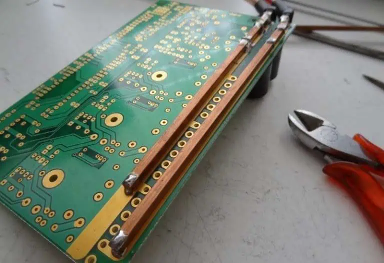
It is a widely used substrate substance in the production of PCBs and can be coated or uncoated. It is popular in the industry due to its cost-effectiveness and reliability.

FR-4 comprises a mineral filler, glass cloth & epoxy resin that laminates together. A Glass cloth gives mechanical strength and electrical insulation, while an epoxy resin offers chemical resistance & excellent thermal properties.

Due to its mechanical properties and cost-effectiveness, the fiberglass-reinforced epoxy composite is widely used as a substrate substance for printed boards. Furthermore, its good dielectric properties make it a suitable coating for PCBs.

Understand the Fr4 density PCB Industry.

Compared to epoxy glass/polyimide, which has a resin of thirty percent, FR-4 has a lower polish of twenty percent. These results in a lower dielectric constant, giving FR-4 superior signal transmission qualities compared to others.

FR4 is the popular choice among engineers due to its superior signal transmission qualities. This makes a sheet of FR-4 material. A widely used, cost-effective material for constructing electronic device cabinets such as computer racks. Additionally, it is commonly employed in building metal cases for electric equipment like power supplies & motor controllers for industrial actuators or motors.

Is Fr4 density the way to go?

fr4-3mm-PCB

FR4 has several advantages, such as its affordability, lightweight nature, and ability to provide electrical & mechanical stability. Additionally, FR4 is available in a variety of thicknesses. However, it may not be the optimal board substance for all appliances. For instance, when constructing a radio, it may be more appropriate to use high-frequency laminates. It is recommended that you compare the dissipation factor figures of various laminates to determine which one is most suitable for your design.

Why Is the use of Fr4 density in electronics? 

FR4 boards possess excellent thermal properties & remain stable and durable even when subjected to heat, without any warping or cracking.

Besides, Fr4 fiberglass and Epoxy Resin. FR4 fiberglass contains a sheet of fiberglass that provides its structure, while the epoxy resin substrate is responsible for delivering rigidity & other attributes.

The amalgamation of these two substances produces a high-density circuit board possessing excellent electrical properties, rendering FR-4 a suitable choice for insulation on PCBs.

Major Material Types of Fr4 Density

There are various variations of FR-4 based on the material thickness and chemical properties, including the FR-4 & G10. Here are some standard designations for an FR4 printed circuit board substance:

  • Standard FR4:  It is the prevalent form of FR4, offering excellent mechanical & moisture resistance, withstanding temperatures of around 140โ„ƒ-150โ„ƒ.
  • FR4 With High Tg: FR4 with a high glass transition temperature is well-suited for applications that necessitate more thermal cycling & temperatures exceeding 150 degrees Celsius. Standard FR4 can only endure temperatures up to around 150โ„ƒ, but FR4 having high glass transition temperature can bear more elevated temperatures.
  • High CTI: FR4 having high CTI exhibits superior thermal conductivity compared to regular FR4 substances, with a tracking index greater than six hundred Volts.
  • FR4 without copper laminate: A material that lacks copper in its FR4 laminate is non-conductive with remarkable mechanical strength, primarily appropriate for board supports and insulating boards.
  • G10: It is a robust core material with exceptional mechanical qualities, high resistance to thermal shock, excellent dielectric rates, and effective electrical insulation.
  • Fr4 circuit has two layers: The FR4 material comprises an interior fiberglass layer and an exterior epoxy resin layer possessing several properties such as:

Flame Retardant

To enhance their fire-resistant qualities, FR4 materials are blended with flame retardants. Both organic & inorganic treatments can be used for flame retardancy. Organic treatments comprise halogen compounds like bromine, fluorine, chlorine, & iodine, but inorganic treatments contain aluminum trihydrate (ATH). These compounds are useful for treating FR4 materials, rendering them fire-resistant.

Good Electrical Properties

FR-4 is a fiberglass-reinforced epoxy composite possessing commendable electrical properties, stiffness, strength & thermal resistance.

Low Moisture Absorption

FR4 material exhibits a low rate of moisture absorption, which implies that it does not alter its shape when exposed to high levels of humidity. This attribute renders it well-suited for applications in which exposure to moisture is expectable, like electronic devices & electrical components.

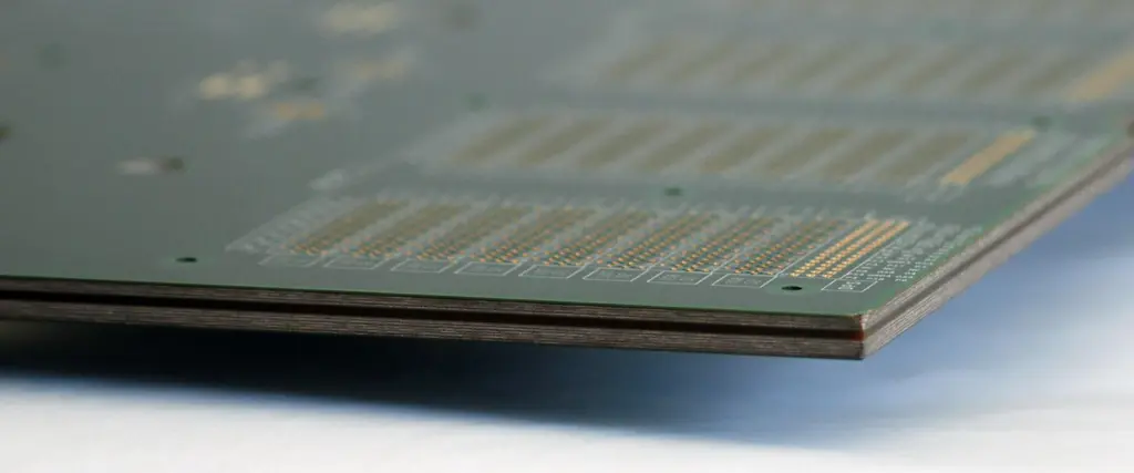
FR4 Material Thickness

When selecting a circuit board fabricator, the thickness(width) of the FR4 substance plays a critical role. Nonetheless, there are restrictions on how thick or thin the design can be. The typical thickness range for FR4 PCBs is between 0.2-3.2mm and changes depending on the product.

Application of Fr4 PCB Density 

FULL PCB MANUFACTURING Quote

Common applications for FR4 are:

  • Industrial Wear Uses
  • Arc Shields
  • Electrical Insulation
  • Transformers
  • Washers
  • Busbars  
  • Switches
  • Relays
  • Standoffs
  • Terminal Strips

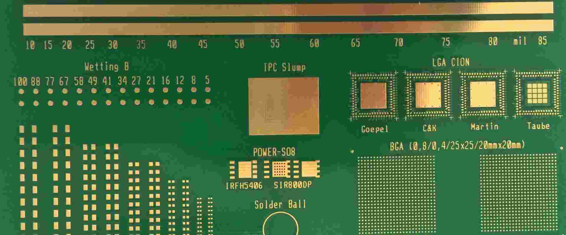
Fr4 density Materials – IPC-A-600 Standards

IPC-A-600 is the guidelines that outline the specifications for producing rigid & flexible PCBs using FR4 materials. The policies cover the surface and subsurface of the base material and apply to all stages of the manufacturing process, including testing and inspection.

Benefits of Fr4 density Materials 

FR4 is a versatile laminate material that boasts impressive mechanical & electrical properties. With more mechanical strength, superior dielectric properties & excellent thermal stability, FR4 is well-suited for a wide range of applications. It is also resistant to chemicals, heat, moisture & most solvents, making it a reliable choice for many industries.

Other benefits of FR4 materials include:

  • FR4 is the cost-effective option over other same substances.
  • It has excellent electrical insulation features due to its greater dielectric strength.
  • FR4 is lightweight with a high specific strength.
  • It is resistant to moisture and has good temperature resistance.
  • FR4 is resistant to water, making it suitable for different PCB applications.
  • The standard thickness for FR4 PCBs is typically between 0.2-3.2mm.

So these properties can make FR4 suitable for use in diverse environments.

Limitations of Fr4 density Materials 

When incorporating FR4 boards into your projects, it’s important to note some of their limitations.

ยท Insulating Stability

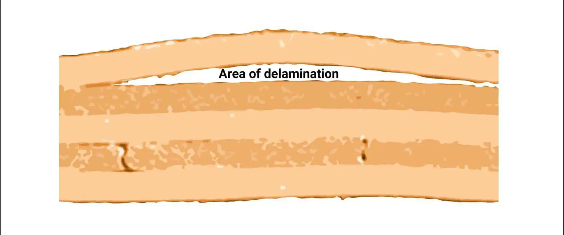
FR-4 circuit boards have excellent insulating properties, but they are susceptible to damage from overloading high temperatures and extra electrical currents going through the circuit board. This can fail the board and cause a loss of proper functioning.

ยท Controlled Impedance

FR4 has a non-uniform dielectric constant that varies as frequency increases, unlike high-speed circuit board substances. High-speed substances have dk tolerances of less than two percent, while FR4 has more than 10% tolerances. Therefore, this poses a challenge in maintaining the impedance (capacitance) values for impedance circuit boards.

ยท Signal Losses

PCB design needs to consider signal loss, particularly in high-speed applications. However, FR4 material is not the optimal choice for these appliances due to its higher Df than high-frequency substances.

ยท Temperature Stability

FR4 boards have a limitation in their ability to withstand high temperatures. While they can handle temperatures up to a certain limit, exceeding this limit can harm the material.

General Properties of Fr4 Density  

FR4-PCB-Material

FR4 substrate has a wide range of features that make it a versatile material for PCBs in various environments. These properties include thermal conductivity, impedance matching, and low heat capacity. As a result, FR4 is commonly useful for most PCBs.

ยท Board Thickness

The PCB thickness is a crucial design consideration, influenced by the board’s size and functionality. Thinner panels are suitable for compact equipment, USB connectors & Bluetooth accessories. However, for larger projects, we recommend thicker boards due to narrow FR4 circuit board limitations. 

ยท Moisture Absorption

Moisture absorption is a crucial property to consider while designing a circuit board. It refers to a material’s ability to resist moisture and determines how much humidity it can bear without degrading. Moisture absorption is measurable as the percentage of PCB material. FR4 has very low moisture absorption, only 0.10 percent when submerged in humidity for twenty-four hours. Hence, it is a perfect option for utilization in electronics fabrication.

ยท Glass Transition Temperature

The Tg of FR-4 falls within the range of 115-200ยฐC, depending on the production process & resins used. Standard FR-4 PCBs consist of an FR-4 layer sandwiched between two laminated copper coatings. One of the advantages of FR-4 is its fire resistance due to the presence of bromine. FR-4 has largely swapped G-10 compounds in an electronic circuit because of its lower price, superior mechanical strength & excellent insulating properties in dry and humid environments.

FR-4 classification and its electrical & physical properties are defined by the National Electrical Manufacturers Association LI 1-1998 standard. Each FR-4 substance has a composition and structure. The primary fiberglass layer provides FR4 with its stability, while the fire-resistant epoxy resin provides its rigidity. Additionally, FR4 exhibits excellent mechanical & insulating properties in both dry & humid environments.

You can use FR4 as a basic insulating material for PCBs. A production company will construct the board on an FR4 circuit board and composite it with a copper sheet to create the final product. PCBs frequently have multiple sides and multi-layer solder resist. These solders resist layers make the circuit for an absolute top overlay layer and allow for V-grooves.


Factors to Consider While Choosing Fr4 density PCB

When selecting an FR4 printed circuit board, various factors should be considered. The most important factor is the durability and quality of a product. While some producers sell the products at a very affordable price, they may not guarantee product quality. To ensure you purchase a high-quality FR4 printed circuit board, it’s essential to read as many reviews as possible before making a purchase. Other factors include:
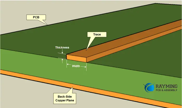
ยท Sheet Thickens

The sheet thickness is a crucial factor in determining the number of layers that your board can have. Thicker sheets are more durable and ideal for high-density interconnect boards.

ยท Impedance Matching

It is a critical aspect of any electrical board, as it ensures that all components of your circuit function together seamlessly without any interference.

ยท Spacing

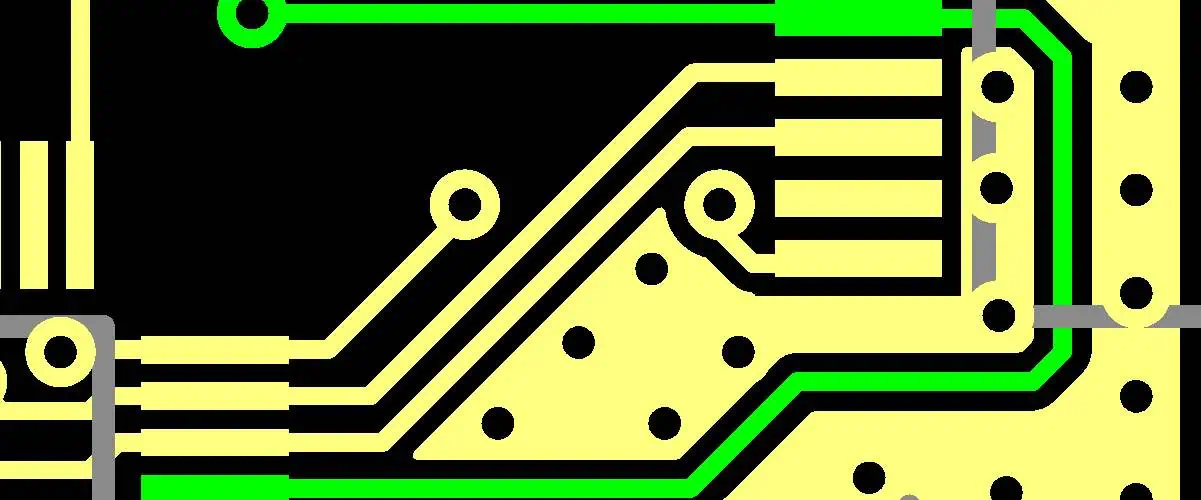
The current carrying capacity of a circuit board is affectable by the spacing between the copper traces. When the trails are too close, the board’s ability to carry current decreases

FR-4 Material vs. Rogers Material 

fr4-tg150
  • The cost of Rogersโ€™s material is significantly higher than that of FR-4 substance.
  • Rogersโ€™s material has superior high-frequency handling capabilities compared to FR-4 material.
  • FR-4 material has a higher dissipation factor, leading to higher signal loss compared to Rogers material.
  • Rogers material offers broader Dk values, making it more impedance-stable than FR-4 material.
  • The dielectric constant of Rogers material ranges from 6.15-11, while that of FR-4 material is approximately 4.5.
  • Rogers substance has a low-temperature variation than FR-4 material.

Wrap Up!

In conclusion, FR4 is a highly advantageous material due to its high strength, low weight & resistance to chemicals and fire. As a result, it has become a popular choice in the production industry.

If you require an FR4 producer for PCBs or boards manufactured by other substances, RayPCB can assist you. We offer quality boards & circuits in all quantities, prioritizing quality and timely delivery.

What is a PCB Dipole Antenna?

PCB Dipole Antenna

In the world of wireless communication, antennas play a crucial role in transmitting and receiving electromagnetic signals. Among the various types of antennas, the dipole antenna stands out as one of the most fundamental and widely used designs. When integrated into a Printed Circuit Board (PCB), it becomes a PCB dipole antenna, combining the simplicity of the dipole design with the convenience and cost-effectiveness of PCB manufacturing. This article delves into the world of PCB dipole antennas, exploring their characteristics, applications, and design considerations.

What is a Dipole Antenna?

A dipole antenna, in its simplest form, consists of two identical conductive elements, usually metal rods or wires, oriented end-to-end with a small gap between them. This gap is where the antenna is fed with the signal to be transmitted or where the received signal is extracted.

Basic Principles

The term “dipole” literally means “two poles,” which accurately describes the antenna’s structure. When an alternating current is applied to the feed point, it causes electrons to oscillate back and forth between the two elements. This oscillation creates an electromagnetic field that radiates outward from the antenna, forming the transmitted signal.

Resonance and Wavelength

A key characteristic of dipole antennas is their relationship with the wavelength of the signal they’re designed to transmit or receive. The most common dipole antenna is the half-wave dipole, where the total length of the two elements is approximately half the wavelength of the operating frequency.

Radiation Pattern

The radiation pattern of a dipole antenna is typically omnidirectional in the plane perpendicular to the antenna axis. This means it radiates equally in all directions in this plane, making it ideal for applications where the direction of the receiving antenna is unknown or variable.

Learn More about:

Typical Dipole Antenna

430-440MHz PCB Dipole Antenna

While the basic concept of a dipole antenna is simple, there are several variations and implementations, each with its own characteristics and use cases.

Half-Wave Dipole

As mentioned earlier, the half-wave dipole is the most common type. Its length is approximately half the wavelength of the operating frequency. This design offers a good balance of size and performance for many applications.

Folded Dipole

A folded dipole consists of a half-wave dipole with an additional wire connecting its ends, forming a narrow loop. This design offers higher impedance, which can be advantageous in certain matching scenarios.

Short Dipole

A short dipole is less than a half-wavelength long. While it’s more compact, it typically has lower efficiency and a different radiation pattern compared to a half-wave dipole.

PCB Dipole

This brings us to the focus of our article – the PCB dipole antenna. In this implementation, the conductive elements of the dipole are etched directly onto the PCB, offering a compact and cost-effective solution for many wireless devices.

Materials of PCB Dipole Antenna

The performance and characteristics of a PCB dipole antenna are heavily influenced by the materials used in its construction. Let’s explore the key components:

Substrate Material

The substrate is the base material of the PCB onto which the antenna is etched. Common substrate materials include:

  1. FR-4: A composite material composed of woven fiberglass cloth with an epoxy resin binder. It’s widely used due to its low cost and adequate performance for many applications.
  2. Rogers RO4350B: A high-frequency laminate that offers better electrical performance than FR-4, particularly at higher frequencies.
  3. Teflon (PTFE): Used in high-performance applications due to its excellent electrical properties, but it’s more expensive than FR-4.

The choice of substrate affects the antenna’s performance, particularly its efficiency and bandwidth. Materials with lower dielectric loss are generally preferred for better performance.

Copper Layer

The antenna elements themselves are typically made of copper, etched onto the PCB substrate. The thickness of this copper layer (often referred to as the “weight” of the copper) can affect the antenna’s performance and durability.

Solder Mask

While not directly part of the antenna, the solder mask layer can influence the antenna’s performance if it covers parts of the antenna elements. In many designs, the solder mask is removed from the antenna area to minimize its impact.

Surface Finish

The surface finish applied to the copper can affect the antenna’s performance over time. Common finishes include:

  1. ENIG (Electroless Nickel Immersion Gold)
  2. Immersion Tin
  3. Immersion Silver
  4. HASL (Hot Air Solder Leveling)

Each finish has its pros and cons in terms of cost, durability, and impact on RF performance.

What is the Range of a Dipole Antenna?

915mhz Dipole Antenna

The range of a dipole antenna depends on various factors, making it difficult to provide a single, definitive answer. However, we can explore the key factors that influence the range and provide some general guidelines.

Factors Affecting Range

  1. Transmit Power: The higher the transmit power, the greater the potential range.
  2. Receiver Sensitivity: A more sensitive receiver can detect weaker signals, effectively increasing the range.
  3. Frequency: Lower frequencies generally travel farther than higher frequencies in free space.
  4. Antenna Gain: Higher gain antennas can achieve longer ranges, but often at the expense of a narrower beam width.
  5. Environmental Factors: Obstacles, interference, and atmospheric conditions can significantly impact range.
  6. Height Above Ground: Generally, higher antenna placement results in better range.

Typical Ranges

For a PCB dipole antenna, typical ranges can vary widely based on the application:

  1. Bluetooth and Wi-Fi: In consumer devices, ranges are typically 10-100 meters, depending on the specific standard and environment.
  2. IoT Applications: Low-power IoT devices might have ranges from a few meters to several hundred meters.
  3. Amateur Radio: Half-wave dipoles used in amateur radio can achieve ranges of several kilometers to intercontinental distances, depending on frequency and conditions.
  4. RFID: PCB dipole antennas used in RFID applications typically have ranges from a few centimeters to several meters.

It’s important to note that these are general ranges, and actual performance can vary significantly based on the specific implementation and conditions.

How to Design a Dipole Antenna

Designing a PCB dipole antenna involves several steps and considerations. Here’s a general guide to the process:

1. Determine Requirements

  • Operating frequency
  • Bandwidth needs
  • Size constraints
  • Performance requirements (gain, efficiency, etc.)

2. Calculate Initial Dimensions

For a half-wave dipole, the total length (L) is approximately:

L = 0.5 * c / f

Where:

  • c is the speed of light (approximately 3×10^8 m/s)
  • f is the frequency in Hz

This gives the length in free space. For a PCB dipole, you’ll need to account for the effect of the substrate, which typically shortens the required length.

3. Choose PCB Material

Select an appropriate substrate material based on your performance requirements and budget constraints.

4. Simulate the Design

Use electromagnetic simulation software (like HFSS, CST, or ADS) to model the antenna and optimize its performance. This step is crucial for fine-tuning the design.

5. Impedance Matching

Design an appropriate feed and matching network to ensure efficient power transfer between the antenna and the radio circuitry.

6. Prototyping and Testing

Fabricate a prototype and test its performance using a vector network analyzer (VNA) and other RF test equipment.

7. Iterate and Optimize

Based on test results, refine the design and repeat the simulation and testing process until the desired performance is achieved.

Key Design Considerations

  • Ground Plane: The size and shape of the ground plane can significantly affect the antenna’s performance.
  • Nearby Components: Consider the impact of other PCB components on the antenna’s performance.
  • Manufacturability: Ensure your design can be reliably produced with standard PCB manufacturing processes.

DIY Dipole Antenna PCB

Dipole Antenna PCB

For hobbyists and enthusiasts, creating a DIY PCB dipole antenna can be an exciting and educational project. Here’s a simplified guide to get you started:

Materials Needed

  • PCB substrate (FR-4 is a good starting point)
  • Copper foil tape (if not using pre-clad PCB)
  • Etching solution (if creating your own PCB)
  • Soldering iron and solder
  • SMA connector (or appropriate connector for your application)

Steps

  1. Design: Create your antenna design using PCB design software. For a simple half-wave dipole, you’ll need two rectangular copper traces of appropriate length with a small gap between them for feeding.
  2. PCB Creation:
    • If using pre-clad PCB, etch your design using standard PCB etching techniques.
    • Alternatively, cut copper foil tape to shape and adhere it to a non-conductive substrate.
  3. Connector Attachment: Solder an SMA connector (or appropriate connector) to the feed point of your antenna.
  4. Testing: Use a VNA or SWR meter to test the antenna’s performance. Adjust the length if necessary to fine-tune the resonant frequency.

Tips for DIY PCB Dipole Antennas

  • Start with a slightly longer antenna than calculated and trim it to tune to the desired frequency.
  • Keep the feed point connection as short and direct as possible to minimize losses.
  • Experiment with different shapes, such as meandered lines, to reduce the overall size of the antenna.
  • Consider adding a simple matching network (like a series capacitor or shunt inductor) to improve the match if needed.

Remember, while DIY antennas can be fun and educational, they may not match the performance of professionally designed and manufactured antennas. However, they can be an excellent way to learn about antenna theory and RF design principles.

What is the Advantage of a Dipole Antenna?

Dipole antennas, particularly when implemented on PCB, offer several advantages that make them popular in a wide range of applications. Let’s explore these benefits:

1. Simplicity

One of the primary advantages of dipole antennas is their simplicity. The basic design – two conductive elements with a feed point between them – is straightforward to understand and implement. This simplicity translates to:

  • Ease of manufacturing
  • Lower production costs
  • Fewer potential points of failure

2. Versatility

Dipole antennas are highly versatile and can be used across a wide range of frequencies. They can be easily scaled and modified to suit different applications, from low-frequency amateur radio to high-frequency wireless communications.

3. Omnidirectional Radiation Pattern

In its basic form, a dipole antenna has an omnidirectional radiation pattern in the plane perpendicular to the antenna axis. This makes it ideal for:

  • Mobile communications where the orientation between transmitter and receiver is constantly changing
  • Broadcasting applications where signals need to reach receivers in all directions

4. Good Impedance Characteristics

A half-wave dipole has an impedance close to 73 ohms, which is relatively easy to match to common 50 or 75 ohm systems. This simplifies the matching network design and improves overall system efficiency.

5. PCB Integration

When implemented on a PCB, dipole antennas offer additional advantages:

  • Space Efficiency: The antenna can be integrated directly into the device’s PCB, saving space and reducing the need for external components.
  • Cost-Effectiveness: PCB dipoles can be manufactured as part of the main circuit board, reducing overall production costs.
  • Consistency: PCB manufacturing techniques allow for high consistency between antennas, ensuring uniform performance across devices.

6. Flexibility in Design

PCB dipole antennas can be easily modified and optimized:

  • Meandering: The antenna trace can be meandered to reduce its overall size while maintaining electrical length.
  • Multi-band Operation: By adding traps or using fractal designs, a single PCB dipole can be made to operate on multiple frequency bands.
  • Polarization: The orientation of the PCB dipole can be easily adjusted to match the required polarization.

7. Good Efficiency

When properly designed, dipole antennas can achieve good efficiency, especially compared to electrically small antennas. This translates to:

  • Better signal strength
  • Improved range
  • Lower power consumption for transmitting devices

8. Bandwidth

While basic dipoles have relatively narrow bandwidth, techniques like broadbanding can be applied to PCB dipoles to increase their operational bandwidth, making them suitable for wideband applications.

9. Scalability

The principles of dipole antenna design can be scaled from very low frequencies (VLF) up to microwave frequencies. This scalability makes the dipole a versatile choice across a wide range of applications.

10. Educational Value

Due to their simplicity and fundamental nature, dipole antennas serve as an excellent starting point for learning about antenna theory and RF design. Many advanced antenna designs build upon the principles established by the simple dipole.

While dipole antennas, including PCB implementations, offer many advantages, it’s important to note that they may not be the optimal choice for every application. Factors such as size constraints, specific radiation pattern requirements, or extreme bandwidth needs might necessitate other antenna types. However, the dipole remains a versatile and widely used antenna design, particularly in its PCB form, due to its combination of simplicity, performance, and cost-effectiveness.

Conclusion

PCB dipole antennas represent a perfect fusion of a classic antenna design with modern manufacturing techniques. They offer a compact, cost-effective, and versatile solution for a wide range of wireless applications. From simple DIY projects to sophisticated commercial devices, PCB dipole antennas continue to play a crucial role in the world of wireless communication.

As we’ve explored in this article, understanding the principles behind dipole antennas, the materials used in PCB implementations, design considerations, and the advantages they offer is crucial for anyone working in RF design or wireless communication. Whether you’re a hobbyist looking to create your own antenna or an engineer designing the next generation of IoT devices, the PCB dipole antenna is a powerful tool in your RF toolkit.

As technology continues to evolve, we can expect to see further innovations in PCB dipole antenna design, pushing the boundaries of performance, size reduction, and integration. The fundamental principles, however, will remain the same, underscoring the enduring relevance of this elegant and effective antenna design.

Microcontroller Vs FPGA: What are their Differences and Similarities?

Microcontroller Vs FPGA

A microcontroller shares some similarities with a field programmable grid array (FPGA). However, some differences exist between both programs. While both are basically integrated circuits embedded in devices and products, there are some evident differences between these two. Electrical engineers and hobbyists use FPGA and microcontrollers.

These two items can be programmed in such a way that they can perform some particular functions. However, each of these items is ideal for use in different applications. FPGA users can program its hardware immediately after manufacture while microcontrollers can be customized in a higher level. Furthermore, microcontrollers are capable of reading one line of code once which FPGAs can only handle parallel inputs.  

FPGAs are much more difficult to program and expensive since they enable a higher level of customization. On the other hand, microcontrollers are easy to customize and cost-effective. There are more differences between these two integrated circuits. Knowing their differences helps you decide what is suitable for your project. Read further to know their differences and similarities.

What is a Microcontroller?

Microcontrollers

A microcontroller can be described as integrated circuits or a small computer which features similar elements with other computers. It has a central processing unit (CPU), output devices, and some random-access memory (RAM). However, it is different from a desktop computer which is capable of running various programs.  A microcontroller is a special-purpose device that can only carry out one program at a time.

It can perform one function repeatedly or at a user request. Microcontrollers are usually embedded in other devices, irrespective of the type of product. Also, this small computer can run on low energy and as such  its power consumption is in milliamps. Due to its low power consumption, a microcontroller is very affordable. However, the device the microcontroller is embedded in can vary in cost.

Microcontrollers are being used in our everyday life. They are everywhere. These small computers or integrated circuits are embedded in various devices like consumer devices, medical devices and other types of devices. They are embedded in consumer devices like fax machines, monitors, copiers, keyboards, telephones, printers, microwaves, microwaves, and more.

Also, microcontrollers are commonly embedded in devices such as car engine control systems, implantable medical devices, traffic lights, and power tools. Each microcontroller serves a specific purpose. It can use a feedback control system to operate automatically just like the ones used in traffic lights. Also, it can as well function at user request like pressing a button or flipping a switch. A good example of this is your washing machine and microwave.

YouTube video

What is a Field Programmable Gate Array (FPGA)?

A field-programmable gate array functions in a much more complicated  manner compared to a microcontroller. In an FPGA microcontroller, a chip is usually pre-programmed. Therefore, users can change software, but canโ€™t change the hardware. Therefore, users can configure the hardware after purchase.

FPGAs are useful for prototyping  application-specific integrated circuits. Intel makes use of a form of FPGA microcontroller as this helps in streamlining the prototyping process. FPGAs are also embedded in devices and these devices can be altered without any need for a new hardware.  

FPGAs comprise an array of integrated circuits. These arrays are programmable logic blocks. FPGAs arenโ€™t usually configured to serve a particular function at the point of manufacturing. Users can decide to configure and reconfigure it as they want. The configuration process involves using a hardware description language (HDL). FPGAs come with logic blocks which users can combine with interconnects.

The FPGAs used today feature a lot of RAM blocks and logic gates in order to enable complex computations. The hardware description languages used in configuring or reconfiguring the IC are Verilog and VHDL. An FPGA has memory components which include simple flip-flops and complete memory blocks.

Read more about:

What are the Similarities Between Microcontroller Vs FPGA

FULL PCB MANUFACTURING Quote

Microcontrollers and FPGAs serve similar basic functions. These items are developed in such a way that a manufacturer or end-user can determine how they function. FPGAs and microcontrollers serve some particular functions and are designed to be embedded within other devices or products. These two integrated circuits are versatile and as such they are widely used in different applications. These integrated circuits make everything easier thanks.

Microcontrollers and FPGAs have similar appearance. These two integrated circuits are flat  iny chips with several programmable pins.  Basically, they are small computers, specially programmed to serve distinct function.  Therefore, both integrated circuits canโ€™t function as a personal or desktop computer. They rather follow commands to carry out a function at various levels of complexity.

There are other basic similarities between a microcontroller vs FPGA.  The basic components of FPGA and microcontroller are similar. A microcontroller and an FPGA function by using binary and computer logic.

An integrated circuit comprises semiconductor materials. It is capable of storing data and performing calculations. This circuit can make use of an analog or a digital technology. Some FPGAs can switch from analog to digital technology. Digital technology integrates binary logic.

Customization

In terms of customization, microcontrollers and FPGAs can be programmed after manufacture. This means that an end-user or a manufacturer can customize their function and as well embed them as required. FPGAs can be customized to a large extent and as such they are ideal for complicated applications. However, a microcontroller is more suitable for simpler applications.

What is Difference Between Microcontroller vs FPGA?

Microcontrollers and FPGAs are different in terms of their level of complexity and customization. Also, these two integrated circuits vary as regards ease of use and price. Basically, an FPGA enables better customization and retroactive changes to hardware. The process of customizing an FPGA is more complex. Therefore, an FPGA microcontroller user requires more knowledge and skill.

Microcontrollers are very easy to use and are less costly. It is an ideal option for most beginners or hobbyists. However, FPGAs are more suitable for engineering companies. Another difference between an FPGA and a microcontroller is that a microcontroller has a fixed hardware structure while an FPGA doesnโ€™t.

FPGAs comprise logic cells alongside interconnects which can be programmed by making use of HDL coding. Since FPGAs arenโ€™t predefined, users can alter them based on their applications. On the other hand, microprocessors have no fixed hardware structure. This indicates that the processor, connections, memory, and peripheral devices of microprocessors are predefined.

Also, you can easily program the process to carry out a defined task.

Characteristics of Microcontrollers

Microcontrollers feature some characteristics which make them distinct. These characteristics include:

Ease of use

A microcontroller is very easy to use. This is why beginners and hobbyist prefer to use microcontroller. To program a microcontroller, you only need a to have a basic understanding of coding. Also, you can integrate an assembly language such as python or Javascript to program a microcontroller. Coding language like Javascript is very easy to learn through online courses.

Ideal for simple applications

Microcontrollers can carry out simple tasks and as such are suitable for simple applications. For example, when using a laundry machine, you only need to make two or three settings and you are good to go. Also, a computer mouse can only interpret some inputs like right click, scroll up, left click, and scroll down. Therefore, a microcontroller is embedded in such devices.

Affordability

Since microcontrollers are very easy to produce in large quantities, they are less expensive than FPGA. Therefore, they are ideal for use in some applications. Also, they are a perfect choice for hobbyists.

Characteristics of FPGAs

Requires skill to integrate

It isnโ€™t easy to program an FPGA. Users need skill to program FPGA. You donโ€™t only need a knowledge of a coding language, but the skill to track large amounts of variables. Furthermore, you need a understanding of a hardware description language (HDL). Therefore, this isnโ€™t an ideal option for beginners as they canโ€™t redesign and redesign hardware.

Enable Parallelism

There are thousands of logic blocks in an FPGA. All of these logic blocks can be programmed based on your needs. You can create processes without anyone depending on one another.

Higher level of customization

One of the characteristics of FPGA is that it enables users to do more. Also, FPGAs offer a greater level of customization. This means users can program more complicated processes. Therefore, an FPGA is allows more customization than a microcontroller.

Suitable for complex applications

FPGAs are designed for parallel processes. They allow you to integrate more inputs without having any issues. Therefore, FPGAs are suitable for complex applications.

Expensive

FPGAs are more expensive than microcontrollers and as such they arenโ€™t cost-effective.

Enable alteration

After the initial programming of an FPGA hardware, you can still make changes. This allows users to easily change the function of a device without the need to replace its hardware. Therefore, this is beneficial for mass-producing industries.

Which is Better for PCBs: Microcontroller or FPGA?

fpga design

PCBs have conductive layers and such require connections. However, more connections are required if a PCB has more conductive layers. For instance, a six layer board features more conductive layers than a two-layer board. PCB assembly requires technical know-how and skill. Either FPGAs or microcontrollers can be used in circuit boards based on certain factors.

Level of complexity

FPGAs can perform several lines of code and as such, enables parallel processes. This is crucial for highly advanced applications. Also, an FPGA is capable of performing simultaneous operations and handling more complex inputs. However, FPGAs need more accuracy and timing to function appropriately. A little mistake can mess up the whole system.

Microcontrollers, on the other hand, is capable of reading one code at a time. They only process commands one by one. In as much as this can result in bottlenecking problems, there are advantages. Microcontrollers are very easy to reprogram and program. An FPGA can make a simple task more complicated. Repairs will be more complicated if there are any mistakes during an FPGA programming.

Budget

When choosing between an FPGA and a microcontroller, an important factor you need to consider is cost. FPGAs are usually more expensive than microcontrollers. Therefore, if you want to program something simple like a temperature sensor, a microcontroller is a better option. FPGAs are usually expensive at the initial cost, but their expenses reduce later, particularly when they are produced in large quantities.

Level of expertise

A beginner doesnโ€™t need an FPGA since it is very complex to program. Assembly languages are much easier to learn than Hardware Description Language. Since FPGA require a higher level of customization, users need more technical skill. FPGAs are ideal for engineers and designers since it offers then a good level of customizability.

Retroactive alteration

Sometimes, you have to alter your applicationโ€™s hardware for some reasons. In such cases, an FPGA will be a good choice. FPGAs allow retroactive alteration and as such, is highly preferred among several industries.

Microcontroller Vs FPGA Power Consumption

Microcontrollers consume less power compared to FPGAs. The high power consumption of FPGAs is a major concern for engineers. One major problem of FPGAs is that they can go beyond their power limitations and as such arenโ€™t ideal for all applications.

Furthermore, FPGAs are suitable for prototyping and emulation. However, they arenโ€™t as efficient as some components. Due to the unused transistors in FPGAs, they consume high power. Also, extended signal paths increase the consumption of power.

 Microcontrollers consume less power than FPGAs. Most microcontrollers have power-saving or idle modes. Therefore, they are a perfect choice. While some microcontrollers feature sleep currents below 1 ยตA. It is impossible to find an FPGA that has low power requirements. The majority of FPGA systems integrate a microcontroller on the PCB for power efficiency.

Conclusion

FPGA and microcontroller are integrated circuits commonly integrated by hobbyists and engineers. Microcontrollers are very easy to use and are less costly. It is an ideal option for most beginners or hobbyists. However, FPGAs are more suitable for engineering companies. Microcontrollers can carry out simple tasks and as such are suitable for simple applications. Also, FPGAs offer a greater level of customization. This means users can program more complicated processes.

We have discussed a lot of differences and similarities between microcontrollers and FPGAs. With this information, you can now choose which is suitable for your project.

Comparing ENIG Vs. ENEPIG: What’s the Difference?

ENIG PCB

When creating PCBs, every little detail is crucial. A PCB that satisfies specifications is built using a combination of the wire locations, design, and surface finishing touches. However, discussing surface finishing invariably results in an ENIG vs. ENEPIG contrast.

Because they stop the oxidation of copper, which can reduce PCB quality, surface treatments are essential. It might be challenging to decide between the surface finishes of ENIG and ENEPIG. So, how can you make a choice if you are unaware of the potential advantages?

The contrast between ENIG and ENEPIG will be covered in this article. Also, which PCB surface finish possesses the most advantages?

What Is ENIG?

ENEPIG and ENIG
ENEPIG and ENIG

Because of its smooth, planar surface, ENIG has always been a well-liked surface finish of PCB for many years. As a result of the proliferation of fine-pitch Ball Grid Array electronics and other compact surface-mount dimensions, this is necessary for assembly. The method additionally supports several solder reflow phases with the additional advantage of extended shelf-life duration.

However, nickel corrosion has created the “Black Pad” appearance due to past production issues with particular ENIG suppliers. This, however, has been a major flaw in the ENIG finish, but it can be fixed if the right steps are followed.

The nickel deposited underneath the gold finishing corrodes and appears as a “Black Pad,” which is a dark surface. This corrosion may result in the solder pad losing connection to the electrical component pad and a component with poor solderability.

Some PCB producers may find it difficult to generate the ENIG finish. When inspecting the finished item, the gold coating process might cover the finished surface area and hide problems that result in a “Black Pad.” According to the main investigation into the cause of this issue, the nickel contamination that shifts into gold and gives the metal a black tint is most likely the reason.

Through careful observation, your Contract Manufacturer can solve such problems; if no dark bands or spikes appear near nickel borders, a black pad isn’t going to form. A well-managed nickel bath may reduce or even get rid of the flaw. Finally, having a one-year craftsmanship warranty from contract manufacturers like MacroFab gives you additional peace of mind.

Process Implicated In ENIG Surface Finish

The ENIG Circuit board surface coating or finish is a multi-step, drawn-out procedure. To obtain the desired finish, all of these procedures need to be closely watched.

ยท Copper Activation

Keeping the layer of copper active for the electroless nickel deposition depends on copper activation. This step involves cleaning the PCB. This allows for getting rid of dust and oxidation residues. Additionally, moistening the surface aids in removing any trapped gas or air within the perforations.

The producer must take the micro-etching foundation under great consideration. Sulfuric/peroxide is the finest choice. You should also keep an eye on the bath’s life expectancy and operation temperature. The remnants will disappear with a thorough rinsing. Before micro-etching, appropriate rinsing must be performed. The deposits of palladium in the catalysts may react with oxidation.

Additionally, employing a pre-dip catalyst to get rid of any oxidation residues is a good idea. The pre-dip catalyst also aids in the Circuit surface’s acidification.

ยท Electroless Nickel

The ENIG procedure’s next stage is this. Here, the producer creates nickel and sodium hypo-phosphite using nickel sulfate. This mixture acts as a reducer. Moreover, the hypophosphite disperses the required electrons to reduce nickel ions. Additionally, this reaction ought to be enhanced at a precise temperature of 175โ€“185ยฐF.

Furthermore, this facilitates the nickel layer’s deposition on the surface of copper. The nickel acts as an inhibitor or barrier to stop the copper surface from reacting with any other elements.

ยท Immersion Gold

The ENIG procedure comes to a close with this stage. Here, the production of electrons from the oxidation of nickel to the ions of nickel helps to reduce gold in a mixture. Additionally, these electrons reduce ions of gold to a coating of gold metal that protects the nickel. The gold’s thickness needs to match the specified criteria.

Benefits Of ENIG

  • An ENIG coating offers various benefits, which include the flatness of the surface for many fine-pitch Ball Grid Array electronics and different small shape factor components.
  • Excellent for connections with press-fit inserting posts and electrical testing locations in the circuit.
  • Support for edge card connectors and wire bonding.
  • Less expensive contrasting to ENEPIG coating or finishes.

Disadvantages OF ENIG

  • If the gold and nickel processes are not carefully regulated, there is a possibility for “Black Pads.”
  • The electroless gold and nickel plating’s thickness might have an impact on the PCB coating.
  • A wet factor that is relatively low

What Is ENEPIG?

FULL PCB MANUFACTURING Quote

The use of a comparable alternate surface finish, such as ENEPIG, is one straightforward fix for the possible black pad problem. The ENEPIG coating resolves this problem by placing electroless palladium over the layer of nickel. Nickel impurities cannot go from the nickel to the layer of gold because of the palladium. ENEPIG is appropriate for PCBs soldered over a system board that uses various packaging methods. It also offers a broad spectrum of applications, including those in the aerospace, military, and some other high-performance medical devices with great density and dependability.

Additionally, ENEPIG is more expensive than ENIG, but it persists as a cost-effective choice that adds tiny palladium and gold layers for increased toughness and superior solderability. The minimal contact resistance of ENEPIG shields against overheating, energy losses, and inadequate grounding.

Applying ENEPIG Surface Finish

ENEPIG comprises four layers of metal which include nickel, copper, palladium, and gold. The activation of the layer of copper with a layer of displacement initiates the process. The copper serves as an initiator or catalyst in this process.

The two components will then combine after nickel is added to the active copper. This combo will safeguard the copper sheet and stop unwelcome metal-to-metal contact.

A palladium coating is added as part of the third procedure to provide further protection. It’s interesting to note that palladium prevents nickel from deteriorating and dissolving the gold coating. Consequently, a chemical reduction of oxidation will take place during an electroless process, resulting in the formation of a thin nickel and palladium layer.

Finally, submerging the PCB in gold finishes the ENEPIG coating process. And the reason is that gold provides the highest level of security while keeping the palladium safe.

Recall that the layer of Gold will completely cover the board.

Benefits Of ENEPIG

  • Palladium lessens the quality problems of “Black Pad” that some CMs exhibit during the process of ENIG.
  • Preferred for its high solder reflow phases and excellent solderability
  • incredibly dependable in terms of wire bonding ability
  • Has dense vias and satisfies the wide standards of miniaturization and PCB thinness.

Disadvantages Of ENEPIG

  • Being more expensive than ENIG might not be feasible for many applications.
  • Decreased SMT Solder efficiency as a result of a palladium layer that is thicker.
  • more time to wet

Difference Between ENIG Vs. ENEPIG

There are variances between the two surface coatings, ENIG and ENEPIG. Whereas ENIG only employs immersion gold and nickel, ENEPIG uses palladium. In the ENEPIG, the layer of palladium provides high oxidation resistance and electrical performance. ENIG is most suited for usage in low-end electronics, nevertheless. ENIG solely employs the layer of immersion gold over the layer of the electroless nickel. ENEPIG includes a palladium layer between the layers of nickel and gold.

Additionally, the surface finish of ENIG does not produce consistent fold-wire bonding results. This could be brought on by a drop in solder joint dependability. Furthermore, ENIG needs an appropriate procedure to stop nickel corrosion. However, ENIG surface finishes frequently have issues like these.

Similarities Between ENIG Vs. ENEPIG

ENIG surface finishing

Despite the fact that both of these surfaces’ finishes differ. They do, however, have certain things in common. Both ENIG and ENEPIG employ immersion gold and electroless nickel. Both of these surface coatings offer a flat and straight surface. This makes it easier for manufacturers to install components on the surface of the PCB. Additionally, both ENIG and ENEPIG are lead-free. They are, therefore, a green alternative for PCB producers.

Excellent thermal diffusion and electric performance are features of ENIG and ENEPIG. The procedures for both surface coatings are not too difficult. For example, the process of both finishes includes copper activation. The first stage of their procedure is this. The surface goes through a bath of catalyst that contains sulfuric acid and palladium sulfate. This bath creates a foundation for the gold and nickel to deposit on.

The last layer of both surface coatings is immersion gold.

Aspects To Consider While Selecting ENIG Vs. ENEPIG

You have to take a few things into account when picking a surface coating for the PCB. Not every surface finish will work for the PCB needs.

ยท Application Requirement

The surface finishes you choose will depend on the requirements of your usage and application. ENIG is a great option if the application has to operate in hot conditions. This happens because the surface finish offers excellent heat resistance. It can endure very high temperatures.

ยท Cost

This consideration plays an important role. You can pick ENIG if money is a concern. The more costly alternative is ENEPIG. This happens because it includes the usage of palladium.

ยท Pad Flatness

Some Circuit Board surface finishes don’t provide smooth surfaces. This, however, does not happen in ENIG and ENEPIG. Both these surface coatings provide a level surface. ENEPIG or ENIG are excellent options if you need to install extra components on the PCB. Both of these finishes provide thin and uniform layers.

ยท Wire Bonding Capacity

ENEPIG is a great choice in this regard. When constructing a PCB, the capacity of wire bonding is crucial. Additionally, ENEPIG possesses a strong wire bonding capability.

ยท ROHS Compliance

Not all Circuit Board surface treatments adhere to the RoHS requirements. This is due to the presence of some hazardous materials in certain surface finishes. Both ENIG and ENEPIG adhere to RoHS regulations. These surface coatings are lead-free. They are, therefore, perfect for usage.

ยท Shell Life 

The Printed Circuit Board surface finish’s shelf life is crucial. Both ENIG and ENEPIG have a greater shelf life. For up to a year, these surface treatments can be stored.

Conclusion

Surface coatings made with ENIG and ENEPIG are particularly dependable. These finishes meet the requirements for PCB quality. These completed products are the best since they were produced without lead. Additionally, both of these surface treatments provide producers with a level surface. Their workings, benefits, and drawbacks have been described above. Additionally, we contrasted both of these surface coatings.

Coatings made of ENEPIG will prove more advantageous for PCBs with numerous layers. Additionally, ENEPIG is capable of meeting any extra specifications for PCB layouts using various packaging techniques.

Furthermore, ENEPIG can handle touch interfaces without creating issues and is less costly than solid gold. It’s interesting to note that ENEPIG frequently produces PCBs for the military, aerospace, and medical industries. Therefore, ENEPIG is the company to contact if you need wire bonding or push contacts.

What are the High Power PCB Design Considerations and Applications?

High Power PCB Design

As exciting and difficult as the process of PCB design might be, it’s indeed critical to take all required measures to guarantee appropriate circuit performance, particularly when working with the high power PCB Designs.

As the electronic device sizes continue to shrink, design concerns like thermal management and power supply must be considered. This article offers some reliable principles for the designer to follow when designing a PCB for high power applications.

YouTube video

What is a High-power PCB?

There is no formal description of what makes up the high-power PCB. P=IV defines power, and the high power PCB design could be a circuit with high current or voltage elements. The query is, what is the voltage and current threshold for a printed circuit board to be called “high-power”?

Rather than imposing a tight definition on its characteristics, it is simpler to classify high-power PCBs based on issues that may develop if correct high power PCB design standards are not pursued: electrical shocks and thermal generation.

High power PCB designs in electronics typically conduct current in excess of a few amps. The high-power PCB are the electrical motor drivers that can channel about 30A of electricity inside the circuit. The same is true for the LED driver that could be powering several LEDs arranged in arrays.

High Power PCB Design Considerations

High Power board
High Power board

Trace thickness and width

In general, the longer your track, the higher its resistance as well as the heat that gets dissipated. Because the purpose is to reduce power losses, our recommendation would be to keep those traces which conduct large currents as small as possible so as to guarantee high reliability as well as endurance of a circuit. Designers can use the calculations in IPC-2221 standard and the online calculator to appropriately calculate a track’s width, knowing the highest current that can run through it.

This same trace thickness for a normal PCB is roughly 17.5 ยตm (or 1/2 oz/ft2) mainly for its internal layers then 35 ยตm (or 1 oz/ft2) mainly for the exterior layers and ground planes.

To decrease track width when using same current, high power PCBs often employ thicker copper. This decreases the amount of space taken up by the PCB traces.  

PCB Layout

Before running the very first trace on the high-power circuit, it’s indeed critical to have high-level knowledge of its layout. Also, the layout of the board should be addressed from the beginning of Circuit board development. Determining the power’s path is an important criterion that pertains to every high-power PCB.

The placement as well as amount of electricity flowing via the circuit is crucial factors in determining how much heat the Circuit board must dissipate. The following are the primary aspects that influence the PCB layout:

  • power going across the circuit
  • The ambient temperature within which the circuit board operates
  • the quantity of air movement influencing the board
  • the material utilized to manufacture the PCB
  • Density of the components populating the board

Placement of the Component

It is critical to initially determine the location on the Circuit board of the high-power components, like power transistors or voltage converters that generate a significant quantity of heat. The high power components shouldn’t be put near the board’s edges, as this produces heat buildup as well as a large increase in temperature. Fully integrated components, like microcontrollers, FPGAs, and processors, should be inserted close to the center of a circuit board to allow for homogeneous heat diffusion over the board thus, as a result, a reduction in temperature.

To prevent the production of hot spots, its power components shouldn’t ever become concentrated within a single region; instead, the linear type design is recommended.

Thermal management

In order to keep every component within acceptable temperature limits, appropriate thermal management becomes required. Never allow its junction temperature to surpass the limit specified in the datasheet of the manufacturer (usually within +125 ยฐC to +175 ยฐC for the silicon-based devices).

That heat created by every component is transported outwards via the package as well as connection pins. Manufacturers of electronic component have created increasingly thermo-compatible packaging in past years. Despite these advancements in packaging, heat dissipation gets more challenging as the integrated circuits’ size shrinks.

Solder Mask

Another method for allowing a trace carry more current is removing its solder mask out of the Circuit board. This reveals the copper material that may be reinforced with extra solders to enhance copper thickness and lower overall resistance present in the PCB’s current-carrying components. This approach allows the PCB traces handle more power and without increasing trace width.

Material selection

Electronic circuits that suit high-power applications necessitate not only efficient design strategies, but the PCB materials that can dissipate the considerable quantity of heat generated by these components. As a result, high power Circuit boards employ materials with minimal losses as well as high-thermal conductivity.

Thermal conductivity, which suggests how successfully heat travels via a material but also can be expressed in form of power watts for every meter of the material as well as per degree Kelvin, can be described as one of the major parameters that influence material selection. Copper, for example, has a thermal conductivity value of 400 W/m/K and can transfer the thermal energy extremely quickly.

Including Safety Features in a High Power PCB Design

FULL PCB MANUFACTURING Quote

A major concern regarding high power PCB designs, as with all other circuits, is its ability to function safely. There are some potential issues which are unique to boards which drive those types of high-powered loads. This same primary danger is heat.

The main danger is heat. Regardless of the quality of design as well as lay out that board, it generates more heat than the standard boards. This ought to be constantly considered when building the housing, as well as external fans/vents should be used.

Overheating is a legitimate concern in the high power PCB design. The risk of a load short-circuiting as well as drawing excessive currents from the regulator or MOSFET is also present. Detect such incidents by including suitable security features in such a design.

When placed near heat-generating components, the temperature sensors will be useful. It sends alerts whenever the Circuit board temperature surpasses a safe level. Place fuses somewhere at high current outputs to ensure short-circuit safety to guarantee that connections are immediately cut off, whenever there is a rise in current above the safe threshold.

More safety features

Short circuits constitute the following potential safety hazards. Because the board has been designed for driving high-power devices, this can source a significant amount of electrical current when shorted. This possibility must be taken into account during the stage of design. The simplest method for dealing with shorts involves having a fuse present on all the outputs as well as the input fuse.

The fuse ratings should always be less than what the wires can handle. Also, they ought to be evaluated for a lower or equal current that the board pours/traces have been designed for. Additionally, it’s a great idea to utilize drivers which have in-built short-circuit protection.

While working on the high power PCB designs, you’ll require a reliable PCB design software. If you’re working with OrCAD, you’ll discover that implementing the above techniques we mentioned is a simple process having the necessary tools at your disposal.

Techniques for Creating a High-Performance PCB Design

Layers should be doubled

One technique I’ve used with several high-powered circuits but haven’t seen much is having the double-layer copper pour as well as stitching them altogether with vias. Such a double module enables twice as much copper to become present within a single area. iFor such a board, we doubled the copper from its terminal into an input fuse onto the main power input.

Make use of copper pours

I always attempt to utilize copper pours with all the power nets, regardless of the board type I’m designing. When working with dedicated high-current designs, all high power nets ought to pour. Also, copper pours boost the copper width that fits on the board significantly.

Recognize the trace width calculators

When designing a circuit board, users must be aware of the least trace width. It’s particularly crucial when working with the high power PCB designs. I have no particular favorite calculator because they should be based on just one IPC-2221 formula. The calculator will be used on 2 major high-current nets on this board.

The initial is the major 30A supply, which runs from the power supply towards the fuse and then branches.

Make use of thermal reliefs

There will always be some disagreement when discussing thermal reliefs throughout high power PCB design. When soldering, thermals are used to prevent heat from wicking to your surrounding copper. They do a good job of it. They have the drawback of having very little copper available for current flow. Also, for the standard PCB, this is usually a small concern, and these thermal advantages far outweighs the disadvantages.

PCB High Power Applications

High Voltage PCB

Electronics are now an indispensable component of our everyday lives. We want electricity for everything, including smartphones and home appliances. The PCBs are electricity’s major factor.

It serves as the foundation for the majority of today’s electronic devices. This adaptability allows PCBs to be used in a wide range of capacities and applications. We’ve discussed some applications in more detail below:

Medical Equipment

All electronics plays an essential part in the medical industry, serving as control, diagnostic, as well as treatment systems. Also, as electronics are becoming more compact and powerful, medical applications for these devices expand, opening up a variety of fresh possibilities.

Circuit boards in the healthcare profession are highly technical in order to comply with the particular constraints of the medical equipment. Medical PCB, which is also known as the HDI PCB, seems to be specialties of high-density interconnect PCB.

Customizable base materials may additionally be manufactured from the medical PCBs, enabling PCBs to be able to flex while in use, which is useful for both exterior and internal medical devices. Also, aside from adhering to strict medical regulations, the suppliers of medical PCB must demonstrate repeatability and dependability. The following are some of the common medical Printed circuit boards:

Monitors: Health and personal care monitors include blood, heart rate, glucose, as well as monitors of blood pressure.

Chemical Equipment: Medical science employs a variety of scientific methods for studying illness as well as testing patient effects. These include photometers, electronic microscopes, as well as compressor and generator control systems, among other things.

Consumer Electronics

Computers, smartphones, and a variety of consumer goods rely on Printed circuit boards to function. As electronics became more prevalent in our everyday products, Circuit boards became an integral component of how we live. Companies are producing smaller laptops and smartphones using a variety of novel technologies that include tiny PCBs having high link volumes.

Circuit boards are utilized in a broad spectrum of consumer products, including computers and laptops. In the twentieth century, computers were used in every aspect of life. PCBs are found in laptop and desktop computers. They act as the foundation for many internal computer components. All of these components are linked directly to a motherboard; this can also be called a PCB.

Industrial Equipment

High power PCB design in our industrial sector must also be extremely powerful and robust enough to withstand harsh conditions found in the industrial installations.

PCBs throughout the industrial sector must also be high-powered as well as robust enough to withstand harsh conditions found in the industrial installations.

Conclusion

This article should have provided some insight on the proper tricks and techniques which could be used with the high-powered circuits. There are so many nuances which you wish to look in whenever you are working on the boards; they aren’t much complicated compared to the standard board designs so far the basic “rules” will be followed. The key points are to keep security in mind always, start with a very solid plan, use much copper as possible, and always check the trace width using a calculator.

What is Mentor PCB?

Mentor PCB

The most successful semiconductor, electronic, and systems firms in the world rely on Mentor PCB Graphics Corporation, which is a Siemens company, for its consulting services, products, as well as award-winning support. It is a global leader in the electronic software and hardware solutions. We help businesses create superior electronic goods more quickly and affordably.

Our cutting-edge goods and services assist engineers in overcoming design difficulties in the increasingly complicated chip and board design industries. Mentor operates as the sole EDA business including embedded software solutions and offers the widest range of best-in-class solutions in the market. EDA technology leader Mentor Graphicsยฎ offers both hardware and software design solutions to assist businesses create superior electrical devices more quickly and affordably.

The business provides cutting-edge goods and services that assist engineers in overcoming the design and manufacturing difficulties they encounter in the escalating complicated fields of PCB assembly as well as chip and board design. Mentor Graphics constitutes the sole EDA business with end-to-end solutions for design to production, and it offers the widest range of the best-in-class solutions in the market.

YouTube video

One of the leading electronics businesses worldwide today, Mentor Graphics PCB offers a variety of scalable solutions to cut the time, expense, and risk associated with product design, volume, and NPI production. This Mentor Graphics PCB is the technology and market leader in Circuit board, PCB NPI, as well as optimization solutions for shop floor.

What Mentor PCB Offers?

Functional Checking

Mentor offers its clients vital resources for tackling the increasingly complex concerns of verifying the actual functioning of the complex chip design of today.

The primary reason for design alterations that delay going to market and reduce profitability is functional faults at system level. Design teams should enhance current processes with tools which scale for varying levels of design complexity.

With innovative use models, top-tier technology, and processes, Mentor is revolutionizing verification. Its Mentor Enterprise Verification Platform increases productivity in SoC and ASIC functional verification through integrating cutting-edge verification methods into the comprehensive platform. It supports everything from the block-level simulation into the whole design emulation at the system level.

Design of Integrated PCB-FPGA System

PCB design is evolving to new complexity levels as ICs, ASICs, and FPGAs grow more intricate and PCB manufacturing technology improves to accommodate embedded components as well as high-density connection layers. Design bottlenecks are usually caused by these.

XpeditionTM Enterprise, for the creation of today’s most complex Circuit board designs; the Board Stationยฎ XE, market-standard solution suitable for the PCB design design issues of the multinational company; and PADSยฎ flow, and the top Windows-based remedy for compliant PCB design are just a few of the scalable design solution that Mentor offers to some of the largest system designing companies around the globe.

Mentor also provides solutions for certain design issues such as managing radio frequency design, verifying it, sophisticated packaging, continuous team design, integrating FPGAs onto boards, and managing design data.

Solutions for Automotive EE Design

Nowadays, a new automobile has 15% more technology in its entertainment, navigation, as well as safety systems compared to cars from a year earlier. The demand for technology solutions to handle this complexity develops as the systems for electrical wiring used by the transportation sector become more complicated.

OEMs and wire harness producers throughout the world use Mentor’s unmatched selection of cutting-edge solutions. With a data-centric  suite for different electrical systems as well as associated harness designs, the Capital tool of Mentor provides a potent design environment created especially for wire harness sector. Distributed control system development is supported by a systematic engineering approach by Mentor’s VolcanoTM product range.

Electronic Software

Mentor Embedded Softwares Division makes it possible to design embedded systems for a range of applications, such as consumer electronics, medical devices, smart energy, industrial, and automotive sectors.

With the help of commercially supported completely customisable Linux-based solutions, such as the market-dominating Sourcery CodeBench as well as Mentor Embedded products from Linux, embedded developers may build systems using the newest CPUs and microcontrollers. Also, d evelopers may benefit from Nucleusยฎ RTOS’s small-footprint as well as low-power capabilities for actual control systems.

RTL Synthesis

With today’s complicated designs, traditional techniques for hardware design which need manual RTL creation as well as debugging are excessively error-prone and time-consuming. For use in downstream synthesis as well as physical design, the Mentor Catapultยฎ as well as PowerProยฎ solutions automatically create power-optimized and fully-verified RTL.

Using this High-Level Catapult Synthesis Platform, the designers may specify functional intent at a high degree of abstraction but then produce production-quality RTL using industry-standard ANSI C++ as well as SystemC.

Throughout this RTL cycle of development, this PowerPro Low-Power RTL Platform offers a full solution for precisely measuring RTL power use, interactively exploring, and thoroughly optimizing power usage.

Applied Fluid Dynamics

For over 30 industries, the FloEFDTM EFD program offers reliable heat transfer and fluid flow modeling tools. It assists engineers in integrating analysis to cycles without interfering with the process of engineering and is included into top computer-aided mechanical design tools.

HVAC & Constructed Environment

FloVENTยฎ is particularly suited for specialized applications like clean room contaminant management as well as datacenter or warehouse temperature control. FloVENTยฎ invented the modeling of airflow in addition to temperature dispersion within and around the buildings, airplanes, trains, and vehicles. The study as well as optimization of the HVAC equipment may also be done using FloEFD.

Mentor PCB Design into Silicon

Mentor PCB Graphics
Mentor PCB Graphics

Due to increased manufacturing process unpredictability and the expanding size and design complexity that make use of the most recent nanoscale scaling, EDA tools enabling physical design as well as verification had reached their limits. This handoff between IC layout as well as manufacture has evolved with the development of novel process technologies out of a straightforward check into the multi-step processes where this layout design should be improved to guarantee efficient production. This poses several difficulties in terms of photolithography, the data quantities, manufacturing process impacts, and getting a good yield of completed chips from every wafer.

Design teams use Mentor’s Olympus-SoCTM place & route system plus Multi-Corner-Multi-Mode time analysis & DFM-aware design optimization for quick closure of the physical designs to confidently tackle these difficulties. Working with industry-leading integrated Calibreยฎ Mentor PCB Design into Silicon

Working with industry-leading integrated Calibreยฎ Mentor PCB Design into Silicon Every aspect of a design-to-silicon transition is effectively and precisely handled by the Calibre product family. With today’s SoCs, the manufacturing test, yield ramp, as well as debug concerns are addressed by the Mentor TessentTM product suite, this serves as the comprehensive silicon tests and yield analysis platform. Tessent, which is based on the bedrock of the optimal solution for every test discipline, combines them in the potent test flow in order to guarantee complete chip coverage.

The integrated, cost-effective, and user-friendly tool package called Tanner EDA is used for designing, laying out, and verifying analog/mixed signal as well as micro-electro-mechanical systems integrated circuits. Tanner tools, which are used by upwards of 25,000 designers worldwide, offer an end-to-end flow for mixed-signal, top-down, design capture as well as simulation, synthesis including physical design, DFT support, as well as place-and-route.

Software Packages from Mentor to Solve PCB Design Problems

FULL PCB MANUFACTURING Quote

Mentor’s PCB design tools are intended to be inexpensive. Using three different software packages at various pricing ranges, Mentor PCB Graphics has reimagined its tools for PCB design to target various segments of a design industry, some of which it is doing this for the initial time or first time ever.

Engineers in the small as well as mid-sized businesses and members of a solitary team working for a bigger business who are responsible for conducting the whole design, analysis, as well as manufacturing the data delivery of the PCBs may afford the standard product, known as PADS, which costs $5,000.

The three products include PADS Standard, which costs $5,000 including support and includes PCB and schematic layout with the beginning parts library, a component creation wizard, as well as archive management.

Enhanced constraint management, and the high-speed net routing and constraints, the construction and maintenance of the central library, HyperLynx-powered thermal/signal/analog simulation, in addition to the variations design pricing are all included in PADS Standard Plus.

For $18,000 plus support, users may get PADS Professional – and PADS Standard Plus, which includes Xpedition-powered technologies including simultaneous 3D/2D layout, sketch routing, placement planning, net and component explorers, production preparation, and design compare/review.

Mentor PCB Graphics is still marketing their Xpedition multi-seat enterprise-level PCB software. Via its partnership with Digi-Key, it furthermore provides entry-level Circuit board design software at a very cheap cost.

Versions of a technology found inside this Xpedition tools are included into these PADs tools. In order to enable cutting-edge high-speed topologies and design for production, this also incorporates a shared constraint management solution utilized throughout the flow.

Using power/signal integrity analysis, thermal or analogue simulation, designers may virtually prototype the system using HyperLynx product in the application.

Conclusion

One of the leading electronics businesses worldwide today, Mentor PCB Graphics offers a variety of scalable solutions. This is why users of the Mentor PCB has a lot to benefit from.

What is a Test Point PCB?

test point pcb

In a PCB with surface-mount components, a test point pcb is a short wire loop utilized for test probes. They allow the user to monitor the circuitry of the board or introduce test signals during manufacturing. Test points are available in a range of sizes, colors, and materials.

You may make access areas for the test probes using test points. For earlier PCB types with leads, many probes feature J-hooks. The J-hook can be attached to test points in PCB, and the test point’s sharp and pointed end can be used to contact a conductor present on your board. Phosphor bronze is the material used in the majority of SMT test points; however, the silver plate coating is also an option.

YouTube video

What are the Different Types of Test Point PCB?

In a circuit board, the test points are often utilized in one of two ways. The initial is an accessible location that can be easily reached by a professional using portable testing equipment. These places frequently include a soldered post for attaching the test lead to aid with this. For quick reference, the test points in PCB would be marked using the reference designator as well as typically the net’s name in silkscreen, like “GND.”

Furthermore, the other kind of test points in PCB is mainly utilized by automated test apparatus. Through-hole vias, pins, or small metal landing pads that are intended to hold the probes of the automation testing systems serve as the automation testing points on the circuit board. Three primary test platforms using the test point PCB are available. These include:

Whenever the pcb has been constructed, a test known as a “bare board” is carried out to ensure every one of the board’s nets are electrically connected.

In-circuit test

Here ICT is performed after the boards have been put together. The board gets set up on an ICT fixture that has probes for every individual net. Such fixtures typically test the board’s bottom, but they may also test a board’s top or even both sides simultaneously if necessary.

Flying probe

Similar to ICT, the test is performed using test points present on every board net after construction. This flying probe apparatus, on the other hand, employs between two and six roving probes for each test location rather than make use of stationary probes inside fixtures such as the way ICT does.

These are the many test points which will be present in a Circuit board and the purposes for which they are utilized. We’ll learn why such a testing is crucial for the production of circuit boards next.

Benefits of Including Test Points On Your PCB

PCBA ICT TEST

The following advantages will arise from include test locations in the PCB design while it is being developed:

Low profile: Test points in PCB give a substantially lower profile as compared to certain other testing probe connection options. Options like pillars and turrets might not fit inside a compact enclosure. These test points are a more flexible option because of their profile, which is comparable to those of the surface-mounted components.

Time and money savings: When identifying connection problems through test point PCB in the initial stages of design, you may save money and time later. With no early testing, the PCB may exhibit problems at the later design stages that entail more expensive assembly. Testing these sophisticated models repeatedly wastes both money and time.

Error detection made simpler: Test points streamline the entire probe testing procedure, making it simpler to find any problems. You may obtain the measurements that you want using test points in PCB without endangering your circuit board design.

How You Can Design Your PCB Having Test Points In Mind

The following considerations must be taken into account while placing test points correctly:

Board side: Most of the time, having the entire circuit board test points present on one side of your PCB speeds up testing and reduces costs.

Minimum distance of the test points: To improve the effectiveness of testing, test point PCB should be separated by at least 0.100 inches.

Test point PCB distribution: You may more easily check with several probes by dispersing test points evenly around the PCB.

Zone for the tall components: The testing procedure can be made simpler by designating a section of the PCB for the tall components. Keeping these components in a single zone will prevent them from obstructing access to test locations.

Manufacturing tolerances:  While designing the basic layout of your PCB, don’t forget to take manufacturing tolerances into account. During your testing process, the Circuit board will require space to accommodate the test points in PCB as well as probes.

7 Test Point PCB Guidelines to Enhance the Production Process

FULL PCB MANUFACTURING Quote

In a Circuit board with surface-mount components, PCB test points can be described as a short wire loop utilized for the test probes. During manufacturing, they allow the user to introduce test signals as well as monitor the circuitry of the board. The test point PCB comes in different colors, sizes, and materials.

We shall discuss the test point regulations in this post in order to enhance PCB manufacturing. You are invited to check out and study the information below if you are curious to learn more about the PCB point regulations.

7 Rules of Test Point PCB to Remember

The objective of the PCB test point

Setting the test points can be done to determine whether the circuit board’s components adhere to standards and may be soldered. For instance, using a multimeter to measure a circuit board’s resistance is the easiest way to do it. You may know the two ends.

These solder pins of components were in fact employed as the test points inside the initial periods when conventional plug-in was used on a circuit board. The residual coating of the solder paste flux is typically generated on the surface of the solder after the general electronic components are exposed to a wave soldering and SMT tin eating, as well as this film’s resistance is quite high, which frequently results in the poor contact of these probes.

What are the Types of Test Points in PCB?

These test locations on the circuit board will be utilized by three primary test systems:

  • Bare board tests: When the PCB has been created, this test is performed to ensure the board’s nets feature electrical connectivity.
  • ICT is performed after the pcb has been put together. The board would be set up on an ICT fixture that has probes for every individual nets.
  • Flying probe:  Similar to ICT, each test is performed by accessing individual test points on every net of a board after construction.

Limitations of the Test Point in PCB  

Utilizing needle beds in circuit testing has various inherent restrictions, such as:

A needle that has a small diameter can be easily fractured and damaged, and the probe’s minimal diameter has a limit.

Near some high areas, needles can’t be implanted. The high section may be damaged when the probe becomes too near to it. Also, due to the part’s height, a hole must typically be made in the test fixture’s needle bed seat in order to prevent the needle from implanting.

Since every needle must emerge from a hole and have its back end fused with a cable, the space between these needles is likewise constrained. Test points in PCB for all components that are getting harder to fit on the pcb board.

Positive aspects of the PCB test points

Low profile: Test points give a substantially lower profile as contrasted with other connection options of the test probe. Options like pillars and turrets might not fit inside a compact enclosure. The test point in PCB has a profile comparable with those of the surface-mounted components, giving them a very versatile option. Saving time and money: You may avoid wasting time and money later on by identifying connection problems via test point PCB in the initial stages of design. Without initial trials, a PCB may exhibit problems at later design stages that entail more expensive assembly.   Easy error detection

Error detection is made simpler by test points, which streamline a probe testing procedure and make it simpler to see any problems. You may obtain the measurements which you want using test points without endangering the PCB design.

Many applications of the Test Points in PCB

All test points inside the ATP and TP series lines were intended to fulfill a variety of applications, such as:

Hidden test point PCB Issues

More worse are covert issues that compromise the items’ long-term performance. Power consumption and sensor accuracy are two potential problems which could be discovered at populated Circuit board stage but might end up in the hand of the customer untested.

Utilizing test points to identify flaws early reduces costs and improves quality. Also, it provides you with something intangible; which is rest of mind. It might be easy to believe that testing procedures are reliable throughout the production phase, but adding a test fixture increases the level of assurance.

Procedure for creating circuit board test points

This test point has to be an exposed metal area on a board’s outer layer that is wired to a net in order to serve as the test point in PCB. This would make it possible for the probes to interact with it and perform the test. The CAD system’s next step would be to mark the desired places as circuit board test points.

If these test point choices meet the spacing as well as other particular criteria specified in the specifications, the design program will normally proceed and select them automatically. The Circuit board design software would be prepared to convert this data into the test point files once each contender has been marked as test points.

The Importance of Test Points in Circuit Board Manufacturing

FCT Functional Circuit Test

Automatic testing is important for validating PCB manufacturing. ICT and flying probe tests as well as bare board testing ensure that the manufactured board has good connectivity and then verifies the solder connections and the assembly of the board.

ICT as well as flying probe tests achieve that in the following ways:

In-Circuit Test

ICT can be described as a system which makes use of the test fixture created specifically for a particular PCB board design in addition to supplementary software to be employed on this test system. A probe would be utilized for every net upon that design, as well as the software and fixture were made utilizing the test point positions as well as other design data produced by CAD database.

Although evaluating every net to ensure a solid connection to its corresponding part pin is ICT’s primary role, it may additionally be utilized to evaluate the board’s functioning. Developing the hardware and software used for ICT testing are pricey and time-consuming.

These test fixtures were intricate, containing probes in thousands, and altering a fixture to ensure a revised board can indeed be highly expensive. But, once established, this in-circuit test would quickly test a huge number of circuit boards.

The advantages of speed as well as functional testing for mass manufacturing quickly outweigh the expenses and duration of ICT development.

Flying Probe Test

Although this method is similarly intended to check the accuracy of a completed circuit board, it does it very differently from ICT. Between two and six probes fly around the board to access each circuit board test point in place of the test fixture.

This flying probe system may be fitted up extremely rapidly and inexpensively without the requirement to construct an elaborate test apparatus.

The flying probe’s drawback is that it moves very slowly. While the flying probe system must move its probes to every individual test position, ICT could test every spot on the board practically immediately

Conclusion

Setting the test point PCB can be done to determine whether the circuit board’s components adhere to standards and may be soldered. Automatic testing is important for validating PCB manufacturing. ICT and flying probe tests as well as bare board testing ensure that the manufactured board has good connectivity.

Causes of PCB Delamination and How to Repair Them

PCB Delamination

There are numerous potential flaws that could result in a board getting scrapped during manufacture, and especially throughout assembly. Boards would be tested with a variety of heat excursions, toxic chemicals, quality inspections, and cleaning agents while being assembled. There’s a potential flaw in this procedure that is rarely mentioned: PCB delamination.

Delamination, or the beginning of the separation of a laminated board, may happen during assembly when conditions are ideal for the soldering and material parameters. Although no Circuit board is flawless and a limited degree of delamination may happen in some sections of the Printed circuit boards, large-scale delamination needs to be avoided. To achieve this, the materials, reflow profile, pre-bake settings, and laminate storage must be properly matched.

Circuit board fabrication is a challenging procedure that necessitates careful consideration of a number of elements. PCB delamination is among the possible flaws that could appear. Although there are techniques to prevent it, manufacturing mistakes are typically the cause of this problem. We’ll take a deep look at this flaw to discuss its causes, precautions to take, and methods for fixing it. Learn more by reading on!

What Does PCB Delamination Mean?

The base material layers start to separate from one another as a PCB delaminates. Whenever delamination has taken place, its solder mask may seem to have significant areas of discoloration and bubbling if observed on a constructed bare Circuit board or a completely built PCBA. Measling and blistering are two related terms for the same phenomenon – delamination.

The former results in the creation of extremely little delaminated white spots, whilst the latter is almost identical to large-scale delamination. This is an illustration of an image demonstrating PCB delamination upon that surface layer. Where another top materials layer is starting to split from its base material is the roughly round, discolored area.

YouTube video

What are the PCB Delamination Causes

Exposure to moisture and repeated heat excursions are the primary causes of delamination.

Too much moisture

The most frequent reason for delamination is moisture that has been trapped inside the base materials of the PCB. Humidity can increase in laminate materials stored improperly, and too much humidity inside the Circuit board substrate during production might result in delamination. The hygroscopic nature of Circuit board base materials makes water adsorption into the base materials (uncured) simple.

This may occur if the components are subjected to moisture during storage or if the circumstances are humid.

Delamination isn’t usually the result of too much moisture being trapped inside the board, although it will often lead to conducting anodic filamentation. The electrochemical events that result in the formation of tiny filaments in-between these conductors on the PCB include water.

As a result of this development, wires may cross, resulting in short circuits which destroys the circuit board; the water’s presence will speed up the reaction time. Via microscopic examination (often with the scan electron microscope) of the microsection and directly on its surface layer, CAF could be detected.

Thermal Excursions

The time that a Circuit board is kept at extreme temps is an additional topic to investigate. Delamination throughout assembly may result from repetitive thermal excursions to elevated temperatures, especially when the temperature for glass transition is exceeded. After the printed circuit board has been put together, the PCBA may start to delaminate when it is repeatedly subjected to thermal stress over its temperature of glass transition.

Its wave soldering and reflow profile parameters must be checked to make sure there won’t be too much stress upon the materials of a base pcb during manufacturing in order to avoid delamination. Without causing blisters or splitting on the exterior layers, heat delamination could start in the board’s internal layers. High Tg circuit board materials have to be utilized when there is going to be several soldering cycles and if the board is anticipated to experience significant thermal excursions while in use.

Additional Factors

There isn’t always a single reason why delamination occurs. Alternatively, moisture buildup may be caused by a mix of subpar production techniques, inferior materials, as well as other factors. Something as easy as utilizing FR-4 material including the incorrect Tg type could cause delamination.

What are the Differences Between Measling and PCB Delamination?

taconic laminates

Measling is an additional potential issue in addition to delamination. Because they exhibit several similar symptoms, it can be challenging to distinguish between the two diseases. They do, however, have various root causes and signify various manufacturing issues.

Similar to delamination, measling refers to problems relating to the process of lamination. White spots would form on the PCB weave’s interior if not enough resin is put to the circuit board during lamination. The “measles” are the white dots.

If the Circuit board base materials exhibit elevated blisters, this is delamination and is brought on by an accumulation of dampness. White dots, on the other hand, are measling. The shortage of resin while manufacturing, or high stress anywhere at stage in the Circuit board life cycle, seem to be the two main typical reasons.

The board’s performance is probably certainly hampered by delamination. Fortunately, this is not usually the case for measling. Measling in little amounts is widespread. Your PCB may probably continue operating normally so far the measling does not really bridge soldering eyes or conductors.

Measling will probably happen at some point over the board’s lifespan, but it usually doesn’t cause alarm. Measling, however, could also happen during manufacture, just as delamination. While measling will almost probably happen later, manufacturers must use the proper resin-application processes to assure the Circuit board is built without it.

Tests that Measure PCB Delamination

How can I tell if my Circuit board is defective? Delamination frequently starts out invisible since it takes place within. When you start to see blisters on your circuit board, the functionality has probably already been affected.

The majority of delamination prevention and testing methods take place in the manufacturing process. There are several different tests that may be used to assess PCB delamination or find any potential problems with these base materials.

Producers employ a time testing to measure how long this resin requires to detach either from copper or the reinforcement.

This board is heated to a certain temperature throughout the test, and the length of time it takes for delamination to occur is recorded.

Common temperature ranges for this test are 260ยฐ to 288ยฐ Celsius. Generally speaking, a 260ยฐ test was thought to be the more precise of both. Here, FR-4’s Tg rating also has an impact. Higher amounts of Tg in FR-4 delaminates more quickly than lower ones do.

Methods for Preventing PCB Delamination

The first step in preventing delamination is to understand its causes. Delamination prevention during PCB manufacturing seems equally crucial. Many tactics used during the process of manufacturing are part of prevention.

Dry Production Environments

The first requirement is that the manufacturer keeps the production area dry the entire time. Prior to thermal processing, any oxide layer present on the circuit board should remain dry. Otherwise, the heat will cause any moisture to become a gas, leading to delamination.

Suitable Baking

Boards must then be baked before being thermally processed. The oven’s temperature should be higher than the boiling point of water (100 C). Another crucial factor is the position inside the oven. You shouldn’t stack PCBs. Instead, they need room for movement on all sides.

Employ top-notch components

Even with proper production practices, delamination cannot be prevented with certainty. Even if a manufacturer follows all instructions precisely, layer separation may still occur in the boards. In addition to the steps taken, high-quality materials would also be required.

The board’s interior layers need oxide coating. It serves as an essential barrier of defense against environmental hazards and thermal stress.  For best protection, this oxide coating should be placed uniformly across the Printed circuit boards.

Higher quality solder materials

Excellent thermal conductivity (to ensure they can swiftly transport heat between two places) as well as reduced thermal resistance (to ensure that they won’t absorb excessive heat) are requirements for solder materials. Tin/Silver alloy makes the greatest solder since it possesses both qualities.

Improve your assembling methods

It’s crucial to avoid using too much force or pressure while assembling any electrical device because doing so could harm the board as well as make it prone to delamination.

What are the Important Steps for Delamination Repair

FULL PCB MANUFACTURING Quote

Use wipes to clean the blister’s surface. The micro drill and ball mill should be used to drill a minimum of two holes through the delamination blister. These holes ought to be placed across from one another and all the way around that blister. Also, t hey ought to be free of any circuitry or components as well. After drilling, remove any loose material by brushing.

Drilling too deeply could expose its inner circuits or planes; proceed with caution. Also, keep in mind that abrasive processes might cause static charges.

To get rid of any moisture, bake your circuit board inside the oven. Avoid letting it cool prior to actually inserting the epoxy since condensation could occur and trap moisture within once more. Be careful since some electrical components can be damaged by high heat. Take care not to turn up the heat

The epoxy should be poured inside the cartridge and then injected into a drilled hole. The heat inside the Circuit board should assist disperse the epoxy, pulling it inside the vacant area so as to fill up the space.

If such a blister cannot be filled, lightly press the board. Start at its fill hole then move to the hole of the vent slowly. Instead, you may apply vacuum to this vent hole for pulling the epoxy as well as fill any void.

Also, cure this epoxy either for one hour at a temperature of 74ยฐC or 165ยฐF) or for 24 hours at room temperature. Scrape off the excess epoxy with a knife or scraper.

How can you tell whether the PCB is harmed or whether PCB delamination takes place?

Heat

Delamination is present if your gadget feels warm to the touch or becomes too warm when being used. These copper traces present on your circuit board may become detached from its base material due to heat produced by the different electronic components. Short circuits or even fire risks may result from this.

Crackling

Another indication of PCB delamination is if the device emits cracking noises whenever you touch or move it. Little copper foil pieces that come off your board and generate a crackling sound could harm the device’s circuitry and lead to other problems.

Corrosion

Another sign that the PCB has been affected by delamination is corrosion. Delamination-induced corrosion may be the origin of spots on your device’s surface where there shouldn’t be any markings.

Why does the PCB Delaminate when being Reflow soldered?

PCB Multilayer Pressing equipment

The main cause of FR4 PCB delamination during reflow soldering is moisture in the FR4 material, which has swelled and caused the separation of the internal layers.

Ensuring the right material grade is being utilized with the right specifications for the planned assembly procedure is crucial.

Although moisture may cause its FR4 layers to split, the primary source of the issue is frequently a flaw that occurred during the manufacturing process of the PCB.

Since the FR4 material is indeed “Hygroscopic” that will collect moisture from its environment, vacuum sealing is recommended after PCB fabrication. If there are questions about how the PCBs were sealed, they must be pre-baked to remove the moisture before assembly in accordance with the IPC 1601 guidelines.

Conclusion

Hope you understand what causes PCB delamination and how to prevent it. In electronics, PCB delamination can be described as a prevalent issue. It is brought on by a glue holding the PCB’s layers together, which may seriously harm your device’s performance. The good thing is the availability of solutions to stop this issue from occurring! Knowing what and how to check for it will enable you to ensure that the PCB is protected from delamination

Importance and Applications of the PCB Calculator Trace Width

PCB Claculator Trace Width

Trace width is an important consideration in every PCB design. This is why it must be calculated for when designing a printed circuit board. There are factors which determine the PCB trace width during the PCB design process. Trace width is usually calculated and determined after considering some factors.

However, to calculate PCB trace width, one needs to understand how trace width works first. This article explains how to calculate trace width.

YouTube video

What is Trace Width?

A PCB trace connects electrical signal from one junction to another. This junction can be a componentโ€™s pin, a branch off a plane or a test-point designed for probing. The PCB trace width is crucial when designing a circuit board. PCB designers need to determine an appropriate width for their circuit in order to save it from damage as a result of an increase in temperature.

Traces on a PCB have the capability to handle the greatest current load before any failure. When a higher amount of current passes through a path, heat is usually generated. However, the trace will damage the PCB laminate when the current load passes the maximum limit. This can result in a permanent damage of the circuit board.

Traces are believed to be wires that link several components without any resistance. However, this isnโ€™t a fact as all paths on a circuit feature a particular resistance, which gives a crucial consideration when determining the PCB trace width.

It is important to determine the current carrying capacity and resistance to know the appropriate width to make use of. There are several factors that determine PCB trace width. One of which is the increase of temperature applicable to a circuit board. Temperature increase indicates the traceโ€™s hotness when current passes through it. PCB trace widths are usually measured in thousands of an inch or mils.

What is a PCB Trace Width Calculator?

Diagrammatic Representation of Copper Trace

A PCB trace width calculator helps in determining a PCB conductorโ€™s width or trace. This calculator makes use of programmed formulas. Since trace width is a crucial parameter in a circuit board design, it is important to make accurate calculations. Trace width is crucial for passing currents via PCBs while maintaining trace temperature below a particular input value in order to prevent any form of overheating.

A PCB trace width calculator can help you determine different trace components like voltage drop, trace temperature, power dissipation, maximum current, and resistance. You can determine the trace width according to ampere capacity when using the trace width calculator.

Therefore, you have to determine the design specifications in the calculators like the total length of the path, the greatest current in amperage that passes through the trace, and more. After the specifications have been provided, the PCB trace width calculator will generate a calculated trace width.

Trace width calculator determines the minimum width that will match the specifications you provided. The calculated trace width will enable the flow of current without any damage to the circuit board. In reality, internal layers have more extensive trace width than external layers. This is because the internal layers generate more heat compared to the external layers.

Therefore, it is advisable to integrate the internal tracesโ€™ width for the whole circuit board to ensure safety.

How is PCB Trace Width Calculated?

The PCB trace width is usually calculated using a formula. You need to get familiar with some formulas to get started with this process.

Maximum current

To determine the maximum current, you need to use this formula. A= (T x W x 1.378 [mils/oz/ft2]).

Where A is the cross section area, [mils 2] T is the trace thickness, and [oz/ft2] W is the Trace width.

Trace temperature

The trace temperature helps you calculate the trace width. Trace temperature is determined by using this formula T TEMP = T RISE + T AMB. Three parameters help to determine trace temperature. While T TEMP refers to trace temperature, T RISE is the maximum desired temperature rise and T AMB is the ambient temperature

Resistance calculations

Trace resistance is R= ฯ * L / Aโ€™) * (1 + ฮฑ * (TTEMP โ€“ 25 ยฐC)).

Voltage drop calculation

Voltage drop describes the drop in electrical potential as it passes through a current in a circuit. You can determine voltage drop using this formula V DROP = I * R. I refer to the maximum current while R is the trace resistance.

Power dissipation calculations

When the heat produce by an electrical device causes energy loss, there is power dissipation. You can determine power loss by using this formula P LOSS = R * I2

R Refers to resistance while I is maximum current.

PCB Calculator Trace Width Applications

FULL PCB MANUFACTURING Quote

The PCB calculator trace width is crucial for PCB design process. This calculator can help you determine the tracesโ€™ minimum width while passing the required current. Also, the PCB calculator trace width will need your design parameters to determine the required width. Therefore, you will need to provide values for the rise in temperature, trace length, the trace thickness, and current to pass in amperes.

Furthermore, this calculator will offer the necessary results needed for the external trace layers and internal trace layer in the air. Also, these values are applicable to your circuit board design to confirm the functionality of the board.

Also, PCB calculator trace width helps in determining the lowest trace width for power trace and power signal applications. However, the PCB traces transmit calls that make use of small amounts of current. Therefore, you need to consider other PCB parameters to determine the width.

Types of PCB Calculator Trace Width Based on Industry Standards

There are different calculators for determining trace width. All of these calculators function according to industry standards. There are industry standards guiding their calculations. In industrial and commercial applications, the most common standards are the IPC 2152 and IPC 2221.

IPC 2221 PCB Calculator trace width

The IPC 2221 calculator integrates an equation and a single graph to determine the track current. The equation is I=kฮ”TbAc

In this equation, the value of K is 0.0048 for the visible traces while the value of K for the internal traces is 0.024. ฮ”T indicates temperature change measured in Celsius. The value of B is 0.44 and the value of C is 0.725. A in this equation indicates the cross-sectional area.

To determine the trace width with an IPC 2221 calculator, you can integrate only a range of values. The current ranges between 0 and 35 amperes, the track width ranges from 0 to 10.16mm, the copper width ranges from 0.5 to 3 oz, and the temperature rise ranges between 10oC and 100oC. The results wonโ€™t be accurate if you fail to use these values.

IPC 2152 PCB Calculator trace width

This PCB calculator trace width uses a more recent standard for its calculation. The IPC 2152 calculator is more accurate in calculating the maximum trace current capacity via an improved technical approach. The equation used by this calculator is not as simple as that of the IPC 2221 calculator. The IPC 2152 calculator must integrate a Universal chart to know the unadjusted cross-sectional area.

Therefore, this calculator makes use of various parameters to get a series of modifiers. These parameters include the PCB thermal conductivity, the distance between the copper plane and the passing tracks, and the currentโ€™s thickness passing trace.

Guidelines for Calculating PCB Trace Width

Your design specifications and the current that passes via the tracks will determine your PCB trace width. However, there is a rule of thumb to follow for the applications. 10 mm/A is the minimum trace route to apply. This is applicable for a copper thickness of 1.0 oz/ft2.

PCB trace width is more complex to calculate. Therefore, you need to understand some rules when calculating your PCB trace width. The circuit can work on a maximum current, i.e the trace thickness, the ambient temperature, and the unit of the measurement traces. These will determine the widthโ€™s input ranges.

When you input these figures into the trace width calculator, you will get some output figures. The figures you get is the trace width. You can view all the input information on the PCB datasheet or on the physical PCB. You shouldnโ€™t have any guesswork in this case. Any given PCB should contain this information.

The calculator wonโ€™t allow any calculations to be performed if you fail to input the exact measurements and numbers. You may need to use a magnifying glass to view the input information since circuit boards are usually tiny.

How to Ensure Efficient PCB Trace Width

Minimum width/Spacing

Determine the standard track width

You should determine or know the size of your standard track you will be using within the design. Your circuit will likely experience shorting if the standard track is too close or too narrow. There can be restrictions on the number of tracks in a particular area if the tracks are far apart. In this case, you may have to integrate additional planes in the circuit boards to be sure the circuit board can be routed.

Determine the circuit pad shapes

Component libraries usually feature libraries for PCB footprints and schematic for various components. However, these depend on the manufacturing process. You need to determine the manufacturing process before starting the design. Therefore, you can easily select the optimum pad sizes and then integrate it on the PCB CAD system.

Evaluate the track size for lines carrying current

PCBs have thin tracks which can carry a limited current. Therefore, you need to consider the trace size for any track that transmits power rails instead of low level signals.

Determine the dimensions of the hole and pad

It is crucial to determine the dimensions of the hole and the pad once you commence the PCB design. In most cases, the pad to hole ratio is 1:8. Sometimes, a pad that is larger than the hole can be used to measure. The PCB manufacturer can give you the required standards for their own process. As the holes and padsโ€™ size decreases, the ratio becomes very crucial.

What to Consider when Deciding PCB Trace Width and Spacing Values

PCB trace widths can impact the performance of a circuit board in several ways. There are factors to consider when deciding PCB trace width value.

Signal integrity and electrical performance

Most digital routing on PCBs already have default value for their trace widths, however, some nets need various sizes. For example, controlled impedance nets require the calculation of their trace widths according to the PCB layer stackupโ€™s consideration.

Sometimes, analog routing may need unique trace widths based on the applications of the circuitry. In some scenarios, you may reduce the default trace width in tight areas. However, you need to ensure it doesnโ€™t extend across the printed circuit board.

PCB fabrication

A PCB trace is easier to fabricate if the trace is wider. The etching process has a much better effect on long and isolated traces. Therefore, it is advisable to make the traces wider. For instance, a 20 mil trace will offer better tolerance compared to a 3 mil trace. Also, the copper weight determines the trace widths.

Power and grounding routing

Traces used for power and ground routing must be wide enough to conduct higher amounts of current. Traces can get really hot and burn through if they are very thin. Also, power traces on the PCBโ€™s internal layers should be wider to ensure heat dispersal. Power traces routed on the external layers donโ€™t need to be too wide since exposure to air can help to cool off.

Traces integrated in power supply circuitry should be kept short and wide enough to handle the current. Ensure the spacing for traces carrying greater amount of current is more.

Conclusion

A PCB trace calculator can help you determine different trace components like voltage drop, trace temperature, power dissipation, maximum current, and resistance. You can determine the trace width according to ampere capacity when using the trace width calculator. We provided information about PCB trace width calculator and we hope this information helps you in determining your PCB trace width.

A Closer Look at Flexible Substrates and Their Significance

flexible pcb circuit board

Technology today comprises complex internal components that facilitate the transmission of numerous signals among the user’s inputs & the system’s Storage. With the development of smaller & more manufacturers, advanced devices need elements that can withstand the stresses and demands of various conditions and applications.

In earlier decades, technology was constrained by inflexible internal parts that could clasp under high Degrees of tension. In environments with excessive heat and vibration, any device containing PCBs would quickly fail. Nevertheless, technology has made significant progress recently, thanks to the advent of flexible laminates.

What is Flexible Substrate?

A flexible laminate is a thin, heat-resistant material, typically composed of polymers such as polyimide & polyethylene terephthalate. In modern computing or electronic gadgets, the miniature PCBs that convey signals among the control prompts & screens are frequently fabricated using flexible substrates.

Manufacturers have progressively adopted flexible substrates for printed circuit boards because of their pliable characteristic, which facilitates their insertion into narrow and tight spaces. Additionally, PET laminate can endure the temperatures and stresses of a broad working environment while offering average frequencies with low components.

Major Uses of Flexible Substrate 

flexible-circuit-board-manufacturers

The versatility of flexible laminate materials has led to their application in numerous industries, including the industrial and medical sectors, for various technologies and uses. The Adaptability and robustness of the substance make it ideal for compact devices and challenging working environments. Here, factors such as vibration and extreme heat are commonplace. Here are the principal benefits of flexible substrates:

ยท Automobile Features

As modern vehicles rely more on technology, they increasingly adopt flexible substrates in the car industry. With the emergence of cars, automakers require methods of integrating diverse smart elements into a car structure without adding weight to vehicle design.

Flexible substrates enable automakers to equip modern vehicles with Wi-Fi connectivity, sensing capabilities, and voice commands. Additionally, due to the affordability of flexible components, automakers can add these features at reasonable prices. Furthermore, flexible laminates can withstand the diverse vibrations and tremors associated with the bumps & rough terrain found on the country’s open roads.

ยท Electronics

The current trend toward devices has led manufacturers to produce electronic and computing gadgets that are smaller than ever before. This advancement has been made Achievable by PCBs that can be inserted into small gadgets that can fit comfortably in the palm. Thin, light devices such as smartphones, tablets, miniature video recorders, and digital cameras use flexible substrate PCBs.

ยท Microwaves

Devices that create high temperatures require components that can withstand extreme heat levels while remaining flexible and durable. Consequently, flexible laminates have become essential in the functioning of ovens. Every time you heat a cup of coffee in under 60 seconds, a series of processes are facilitated by substrate PCBs. It sends a message from the button you press to start the microwave, which makes the microwave produce heat and warm up your food or drink.

ยท Industrial Applications

Machines that operate along conveyor belts in factories & processing plants experience a significant magnitude of anxiety throughout the workday. Previously, these devices depended mainly on electricity & compressed air energy since PCBs were too sensitive and cumbersome for the rigors of the industrial environment. However, due to the robustness and thermal resistance of substrates, computing technology can now be integrated into industrial machines, allowing them to carry out a wide variety.

 Of Intensive procedures.

ยท LED Lighting

Flexible substrate PCBs have addressed the concern of heat generation in LED lighting systems, which has been one of the main issues associated with this lighting technology. Despite competition from other lights, LED lighting has gained popularity due to its energy-saving and efficient features. Using flexible substrate printed circuit boards has eliminated the wastage of energy and temperature impacts on working environments.

ยท Medical Devices and Implants

Because of their miniature size and pliable characteristics, PCBs fabricated with this ultra-thin substrate have become a crucial component in modern medical devices. Flexible substrates(laminates) are now utilized in a wide range of applications, ranging from surgical instruments to electronic Embeds.

ยท Power Electronics

Flexible substrates, when Joined with thin layers(copper), find application in the power electronics industry. They are particularly important for high-power devices that require stress-resistant durability to operate at maximum capacity.

Use of Flexible Substrate in Printed Circuit Boards 

FULL PCB MANUFACTURING Quote

Multi-layered circuit boards containing integrated circuits, interfaces, and microchips can be fabricated using flexible substrates. These circuit boards have a similar appearance to modern PCBs that are simple, sleek, and unencumbered. However, the key difference is their flexibility and ability to bend significantly without compromising functionality.

Flexible substrate PCBs require a less array of elements compared to traditional PCBs. Despite its compact size, this equipment can achieve high-density functionality with just a Minimal amount of surface area. As a result, flexible substrate printed circuit boards are good for small equipment that needs high-performance capabilities for multiple functions.

The flexibility of substrates makes them an ideal choice for PCBs, as they can withstand vibrations, tremors, and high temperatures without compromising their functionality. Despite these stress factors, flexible substrate printed circuit boards maintain their high-performance capabilities. This makes them particularly useful in challenging environments such as factories and power facilities, where they can deliver average signal integrity.

Flexible substrate PCBs operate with minimal mistakes as they lack wiring components and mechanical connectors, which can introduce errors. Additionally, their assembly methods are relatively uniform, making them compatible with various devices. Flexible substrates enhance the reliability, robustness, and high-performance capabilities of PCBs, which is why modern manufacturers increasingly prefer them over rigid PCBs.

Amazing Advantages of Flexible Substrate

Bendable materials provide significant advantages to printed circuit board manufacturers & the businesses or organizations that utilize them in their Advanced computational systems. The flexibility of substrates makes the boards easier to uninstall, install, handle, and repair, reducing their overall complexity. Additionally, flexible substrate components are cost-effective and easier to manufacture than rigid PCBs. Overall, the Advantages of Flexible materials can be summed up as follows:

1. Reducing Weight and Space

Flexible substrates are easier to integrate into a wide range of Digital devices due to their reduced size and weight. They can be Set up in even the smallest computing equipment available today. The light weightiness of flexible substrates makes them ideal for motherboards for laptops & all-in-one devices. Printed circuit boards made of flexible substrates can significantly reduce space volume by up to 50% and decrease weight by 90 percent making them highly advantageous for many applications.

Flexible laminates are particularly well-suited for use in the aerospace & medical industries. In hospital equipment, the lightweight nature of flexible substrates enables the construction of more compact yet intricate devices that can be easily moved from one room to another. Similarly, the lightweight and compact characteristics of flexible substrates make them the ideal choice for devices used in air travel.

2. Easier Installation and Service

Flexible substrates can be easily installed by flexing and bending them into a printed circuit board. This flexibility greatly reduces the difficulty and labor of assembling some of the smallest boards and devices. As a result, using flexible substrates generally results in lower manufacturing costs. Additionally, maintenance and servicing devices with flexible laminate components are easier, as the material can be easily manipulated for repairs and modifications.

3. Increasing Reliability

Flexible laminates are more reliable than earlier altered markets due to their minimal interface connections. With a flexible substrate, there is less reliance on connectors, solder joints, solder, and other interface components, reducing the possibility of failure. Additionally, flexible substrates possess the strength to withstand the impacts of vibrations, heat, and shocks, making them suitable for boards used in devices designed to cope with high temperatures and turbulence. As a result, devices with Bendable bases

 are generally robust enough to withstand even the most grueling military & medical applications.

4. Managing Heat

Flexible substrates offer exceptional heat resistance and flexibility compared to other options, making them suitable for device components that face higher temperatures in humid environments. And industrial These substrates can resist temperature changes that cause other materials to expand and contract over time. Additionally, flexible substrates are largely resistant to the effects of gas, oil, acid, UV exposure, and radiation. This makes them a reliable choice for devices used in harsh environments, such as in the military and medical fields.

5. Improving Aesthetics

The transparent look of flexible substrates not only enhances the aesthetic appeal of electronic & computing devices but also makes it easier to identify the internal parts. In the past, internal parts of electronic components were often hidden behind wires & elements, making it difficult for non-experts to identify them.

With flexible laminates, the internal parts of newer components are more visible, making them less intimidating for the optimal user. In industrial settings, IT personnel and computing staff can quickly identify flexible laminate parts since wires and other through-hole elements don’t protect them.

6. Eliminating Connectors

Flexible substrates eliminate the need for interface connections in electronic and computing components. They can also accommodate most elements if they apply to rigid printed circuit board design. PCBs with flexible substrates are flat or sleek in Look

As a result, they can be easily put in slots in small devices because of the absence of Intricate interconnects

7. Reducing Assembly Costs

Flexible substrates’ thin and lightweight nature makes them easy to use in tight spaces, which reduces the overhead costs associated with manufacturing components. Additionally, using flexible components substrates can lower packaging and material costs.

Future of Flexible Substrate in Electronics Industry 

Shortly, flexible substrates witness a surge in their application across various fields, such as electronic memory. PET substrates, which offer both durability and flexibility, will likely drive further technological progress in light control, memory storage, and signal transfer within the computing and electronics industries.

Using flexible substrates in PCBs for computing equipment can significantly advance memory storage for small devices. It is possible that in the future, manufacturers could produce thumb-sized equipment with the capability to store high-quality movies & run many programs simultaneously, all through the use of voice commands. These tools could be Suitable with large screens that display high-resolution, full-color images and come equipped with integrated speakers. The control of these features is manageable remotely through voice-activated Artificial Intelligence technology. It is all possible due to the implementation of substrate-printed circuit boards.

Using PET flexible substrates drives progress in the smart car industry. With the increasing likelihood of driverless cars dominating the roads shortly, flexible printed circuit boards will play a critical role in enabling high memory capacity, advanced sensing technologies, artificial intelligence, or remote connectivity in these vehicles. Moreover, Similar technology is leveraged in airborne power vehicles. It is potentially reducing reliance on conventional transportation infrastructure such as bridges and roads.

Bendable base materials will likely be crucial in developing futuristic technologies such as robot maids and delivery drones. With a decreasing reliance on cars and expanding businesses through the Internet, clients can order food and clothing from far-off restaurants and shops through drones. These flying robots may rely on flexible circuit boards that have a large capacity, can handle stress well, and are long-lasting.

Flexible Substrates from RayPCB

More and more manufacturers are realizing the advantages of flexible laminates and are switching to them as an Element for PCBs. With flexible printed circuit boards, even the tiniest devices are furnishable with greater power and durability than The bigger versions. We offer a variety of flexible boards. Contact us today to learn how flexible substrate-printed circuit boards can help your devices perform better. We’ll be happy to share all the details with you.