Component placement is a very important aspect of PCB assembly. There are different ways of mounting components on a circuit board. Each of these approaches has its benefits and disadvantages. The type of mounting technology used in a circuit board determines its functionality.
Sometimes, the application requirements determine the type of mounting technology to use. It is important to know how these technologies work. Therefore, this article will shed more light on the difference between SMT, THT, and SMD.
THT VS SMT
THT and SMT are the two major types of mounting technology for PCB. These technologies are used in mounting electronic components on circuit boards. However, there are differences between these two technologies. To have a better understanding, it is important we shed more light on THT vs SMT
What is THT?
THT stands for through hole technology. It is a method of mounting electronic components on circuit boards. THT involves drilling holes through the PCB and inserting the leads via those holes. THT plays a crucial role in PCB fabrication.
This technology involves the placement of component leads into drilled holes on a bare board. Manufacturers solder these leads onto pads on the other side of the board. The manufacturer does this using reflow soldering or wave soldering equipment. THT was a common approach for mounting components until the advent of SMT. Despite the popularity of SMT, THT has proved resilient as it offers several benefits.
THT replaced electronics assembly techniques like point-to-point construction. This technology has been used since the 1950s. The through hole technology is ideal for creating interconnections between layers on boards.
SMT means surface mount technology. This technology is the more recent method of mounting components on circuit boards. It replaced the through hole technology due to certain benefits it offers. SMT involves mounting electronic components on the surface of the PCB directly.
This technology uses automation. SMT makes use of pick and place machines to place electronic components on boards. This technology is considered the second revolution of electronic assembly. SMT uses both wave soldering and reflow soldering to solder components.
The advent of SMT has helped to reduce the cost of manufacturing while maximizing PCB space. SMT was developed in the 1960s and became popular in the 1980s. This technology is ideal for high-end PCBs. The use of SMT has resulted in smaller components. Also, it has enabled the placement of components on the two sides of the board.
In surface mount technology, manufacturers mount electrical components without drilling. These components feature no leads or smaller leads. Here, there is a specific amount of solder paste the manufacturer applies to the board. Since there are not many drilled holes on SMT boards; they are more compact for better routing.
Comparing THT vs SMT
THT and SMT are two reliable mounting technologies in PCB assembly. However, SMT is more reliable and more common. There are differences between these two technologies. While SMT replaces THT, THT is still being used in PCB assembly.
THT inserts electronic component leads into drilled holes on a circuit board. Most times, manufacturers carry out this technique manually. SMT technology doesn’t require as many drilled holes as THT does. The use of pick and place machines in SMT makes the technique much easier for manufacturers.
SMT doesn’t require leads and can be directly mounted on the circuit board. Whereas, THT requires lead wires that manufacturers place in drilled holes. SMT requires advanced production and design skills compared to THT.
THT vs SMT In terms of manufacturing costs, THT involves a higher cost of manufacturing than SMT. However; capital investment for automated equipment is higher than that of THT. THT is ideal for certain applications. Through hole boards are ideal at the prototype stages of a project. For a through hole board, manufacturers don’t need to produce a new solder stencil anytime the circuit board goes through a revision change.
THT vs SMT via through hole technology. This technology is ideal for the manufacturing of bulky components. SMT is ideal for higher circuit speeds since it features fewer holes. Unlike THT, SMT allows assembly automation which is ideal for the production of higher volumes at reduced costs.
SMT provides more board space during assembly, unlike THT which uses up the board space. THT helps manufacturers to check mechanical problems during validation. The manufacturer can fix this problem during redesign without any assembly difficulties. However, in SMT, this is difficult to fix. This is because warp and twist is easier to fix on a manually-assembled PCB.
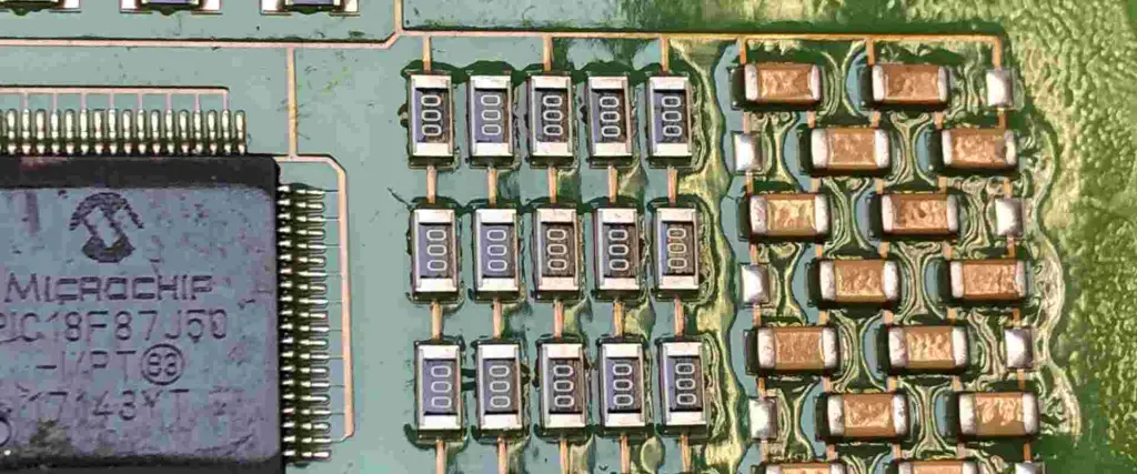
Surface mount device (SMD) is an electronic component placed on a circuit board. PCB manufacturers can place SMD on circuit boards through SMT. There are various types of SMD components. All SMD components work together to enable the functioning of a circuit board. Examples of SMD components include chip resistors, capacitors, and diodes among others.
Let us discuss a few below;
A capacitor is a type of SMD component. This component features a rectangular block of dielectric. The dielectric contains several interleaved metal electrodes. A transistor is another SMD component available on a circuit board. The resistance of this component is built in the ammeter and the base.
SMD resistors are another type of SMD component. There are chip and network resistors. The three digits on the chip resistor are the resistance value. The significant digits are the first and second digits. The network resistor comprises many resistors with similar parameters. This resistor uses the same resistance identification method as the chip resistor.
It is important to know the difference between SMD and THT. A lot of times, most people confuse these two terminologies. Through hole technology involves the soldering of through-hole components on a circuit board. Manufacturers use hand soldering or wave soldering to complete this process. In THT, the component leads pass through the drilled holes on the boards.
SMDs are components manufacturers place on circuit boards through SMT. Manufacturers use solder paste to place SMDs on the bare board. Surface mount devices feature shorter leads that enable a greater electrical connection. THT involves soldering through hole components onto a circuit board by wave soldering. The component leads go through the drilled holes of the boards.
Through hole technology offers stronger mechanical bonding. This technology is ideal for electronic devices likely to suffer from mechanical stress. THT manufacturers use hand and soldering or wave soldering for the THT process.
SMDs are smaller than the components in THT. SMD components can be so small to be clearly seen by the naked eye. Due to the size of SMDs, they save more space on the bare circuit board. SMD components rely on solder balls to enable improved bonding capability.
THT provides more mechanical bonds than SMT. However, the extra drilling in THT makes it more expensive to create the circuit board. Therefore, THT is ideal for more bulky parts. For instance, electrolytic capacitors need extra mounting quality to withstand pressure.
What is the Difference Between SMD and SMT?
SMD refers to the electronic component manufacturers mount on a bare circuit board. SMT is a type of mounting technology PCB manufacturers use to mount SMDs on a PCB. SMT uses a pick and place machine to mount SMDs on circuit boards. This technology replaces the through hole technology.
The advent of SMT has enabled PCB manufacturers to easily mount SMDs on circuit boards. The process of SMT includes solder paste printing, component placement and reflow soldering. The placement of SMD is a very important stage in surface mount technology. SMD and SMT work hand in hand.
SMT enables manufacturers to place more electronic components on the circuit board. This helps to achieve a more compact and lightweight design. Manufacturers prefer this technology due to this benefit. PCBs specifically designed with SMT also offer higher circuit speeds. Hence, these PCBs are ideal for high-frequency applications.
Enhanced mechanical performance
SMT provides enhanced mechanical performance under vibration conditions. Therefore, SMT PCBs are ideal for use in applications extremely exposed to vibration. SMT comprises high-end components which enable multitasking.
Higher densities
One of the greatest benefits of SMT is the ability to achieve higher levels of component density. The high densities are a result of the smaller size of electronic components. Also, the elimination of drilling mounting holes helps to achieve higher densities. SMT uses both sides of the circuit for mounting components.
Quicker Assembly
SMT uses pick and place machines to place components on PCBs. This enables simpler and quicker PCB assembly. Some machines can place over 136,000 components every hour. SMT allows manufacturers to attach components through selective soldering. Manufacturers can also customize the selective solder process for each component.
Low manufacturing costs
SMT reduces the costs of manufacturing printed circuit boards. SMT parts are cheaper that through-hole parts. This mounting technology is a budget-friendly option for PCB manufacturers.
Disadvantages
Surface mount technology replaced THT due to the benefits it offers. However, this technology has its disadvantages too.
Small lead can make it difficult to repair
SMT isn’t ideal for components that produce much heat. This is because the solder will melt under high temperature
The SMT process requires high-skilled or professional operators. Also, it requires expensive automated equipment.
Less solder for solder joints might tamper with the reliability of the solder joints. This is a concern for PCB assemblers.
Through hole technology existed before the advent of SMT. THT has proved to be very useful in some cases. However, it has got its own limitations. Below are some advantages and disadvantages of this technology.
Advantages
Stronger mechanical bond
THT provides enhanced mechanical bonds. This makes THT assemblies suitable for high mechanical or electrical stress environments. Manufacturers prefer to use THT in applications often subjected to stress.
Resistance to wear and tear
THT components can withstand wear and tear. This is because of the solder joints that extend over the board’s width.
Ideal for fast prototyping
THT components are ideal for prototypes and testing. This is because these components are very easy to swap out. THT is suitable at the prototype stages of an application. The prototype layout can make use of THT components to enable quick assembly of the board.
Disadvantages
THT requires the drilling of holes. This increases the cost of production. Also, it takes time to drill these holes, which increases production time.
The drilled holes must go through every layer of the PCB. Hence, THT limits the available routing clearance on a multilayer circuit.
The wave soldering process ensures the soldering of THT components. This process is not as reliable as the reflow soldering process.
Considerations for SMT Designs
The type of materials and surface finish manufacturers use play a crucial role in SMT boards. It is ideal to use more planar surface finish when using finer-pitch SMDs. Manufacturers should ensure they evaluate the base laminate. SMT PCBs need higher soldering temperatures than THT PCBs. This is as a result of the lead-free surface finishes frequently used.
Materials that meet certain standards will withstand high soldering temperatures. These materials also resist several thermal cycling shocks. These shocks may happen when two-sided SMT boards are being assembled. PCB assemblers can reduce the possibility for solder shorts by removing soldermask openings for vias.
With dimensional accuracy in mind, it is crucial to design-in flatness. To achieve this, balance copper coverage from layer to layer and fill large empty areas with copper.
Conclusion
While SMT has been the mainstay of the PCB industry, THT is still ideal for certain applications. THT vs SMT show that the two technologies have got their strengths and weaknesses. The huge difference between SMT and THT lies in their mounting techniques. SMT mounts SMDs on circuit boards without many drilled holes. THT requires component leads and many drilled holes. SMDs play a crucial role in surface mount technology. SMD components are carefully mounted on circuit boards by assemblers.
Printed circuit boards are available in different shapes. There are octagonal boards, round boards, rectangular boards, and other odd shapes. However, the most common shapes are the square and rectangular PCB. Round PCBs are not as common as their rectangular counterparts. With the increasing development in the electronics industry, round PCBs are becoming popular.
Sometimes, there is a need for unconventional PCB shapes. This is because of the need to fit these PCBs into certain enclosures. The fact about PCB design is that a PCB must fit its intended application. Many people aren’t familiar with the round PCB. In this article, we will discuss important facts about round PCB.
What is a Round PCB?
As the name implies, a round PCB is a type of board with a round shape. A round PCB offers an electrical connection to a circuit. This type of PCB is available in consumer electronics, LED PCBA, and more. Round PCBs are ideal for both domestic and commercial devices. A round shaped PCB consumes more time during the routing process. Therefore, these boards may cost more.
PCB manufacturers fabricate round PCBs with extreme care and attention. The fabrication of this type of board is a complex one. A round PCB also features electronic components, traces, and widths. This PCB is available in wearable devices. A round shaped PCB can provide more board space for you. Therefore, this PCB gives you an edge over the rectangular ones.
A round PCB is also referred to as a circular PCB. This type of circuit board is the most difficult to work with. A round or circular PCB is available in tiny wearable devices and rigid-flex circuits.
The designing of a round PCB is more complex than the usual rectangular boards. Manufacturers can only shape the perimeter of this board with a straight line segment. When arranging the lines of the perimeter in a circular shape, you should place a circle on the silkscreen layer.
There are different software for designing a round circuit board. Break routing is the only separation method for a round PCB. Now, let us explore one of these software.
Using Eagle CAD to Make Round PCB
Eagle CAD is a popular software for designing the schematics and layouts of a circuit. A circuit’s schematic is an outline of how various electronic components connect. The designer then converts the schematic into a layout. The layout is the exact image of how the circuit will appear on the PCB. Most times, designers create a rectangular shape layout. However, Eagle CAD has a command that can change a rectangular layout into a circular one. This command is known as “MITER.”
Open the Eagle CAD software to proceed with your design. Click on the “File” and select “Open’ to open the layout file. Click “open” to open the layout file. If you haven’t created a layout file, create a new file. To do this, go to “file” and click on “New.” Name the file according to your choice.
You will need to adjust the board outline’s size according to the PCB’s size. Typically, the board outline will be a square. You can adjust the size by left clicking on either side of the outline and dragging to the right or left. Ensure the shape of the board remains square. This will prevent the shape from taking an oval shape when trying to convert it into a circle.
Make sure the sides of the square are equal to the circle’s diameter. Type “MITER 2” on top of the layout and click “Enter.” The icon will change into a + sign. Left-click on the square’s corner. The corner will become round. If the corner appears too small, use “MITER 3” or any greater number. You can do the same if the corner of the square appears too large. All you need to do is decrease the number of the MITER. Do this repeatedly to round all corners.
There are design rules and strategies for round circuit boards. It is very important you draw out the board’s shape in the CAD tool. This is where the foundation for your board lies. If your round circuit board is for a high-speed device, you will have to design a multilayer board.
It is also important you define the power and ground planes in separate layers. Furthermore, you will need a polygon editor to define the shape of ground or power planes. Certain software will allow you to customize your power and ground planes to fit your round board. For instance, Altium Designer is a software that helps you complete your design.
This software has the necessary tools to help you achieve a great design. The schematic capture of this software is very easy to learn. However, it is powerful enough to create the most complex schematics. Some applications require the need for a round circuit board. Therefore, it is important to design your circuit board to match your devices’ form factor.
The available board space reduces when you use a rectangular board in a curved package. A circuit board will match the packaging’s contour when the designer works with curved designs. Round PCB design provides designers with more flexibility. Also, it can enable you to expand the design to incorporate new features later on. Great CAD and layout tools enable the designer to add pad shapes in circuit boards. Round circuit boards require great panelization schemes for their design.
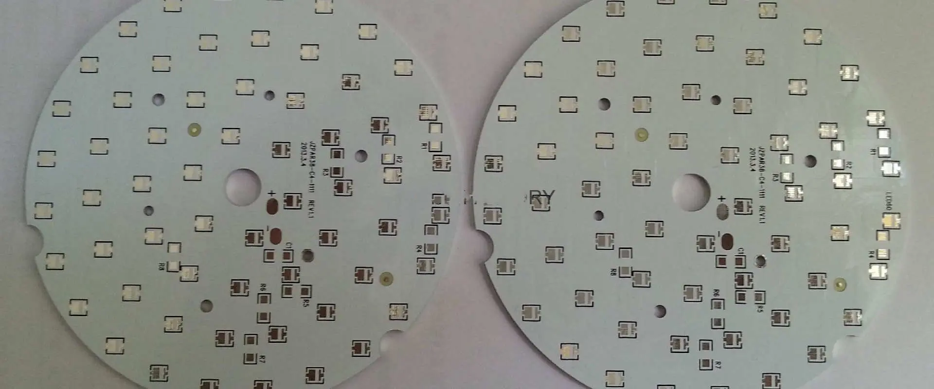
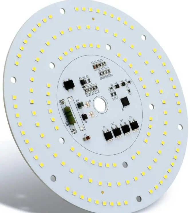
What is a Round LED PCB?
A round LED PCB is a type of circuit board in which a LED is soldered to it. Manufacturers design this type of PCB specifically for LED circuits. A round LED PCB helps to improve heat dissipation. As a result, it allows the greater performance of assemblies. Round LED PCBs are ideal for applications that demand the use of many LEDs.
A round LED PCB features a lot of properties which makes it a great deal in the electronics world. The truth about this PCB is that they have low power consumption. Manufacturers use aluminum to fabricate round LED PCBs. Round LED PCBs are mostly available in light fixtures. For example, these boards are available in a desk lamp, led strip, etc.
Advantages of Round LED PCB
A round LED PCB offers a lot of advantages. This type of PCB is common in several applications due to the benefits it offers.
Round PCBs are ideal for use in several applications. Although the round PCB board isn’t as common as the rectangular ones, it is a great option for some applications.
Medical industry
Some medical devices feature a round PCB board since they offer great benefits. These boards are more durable and lighter. Medical devices such as monitoring devices and hearing aid devices feature these boards.
Wearable devices
The production of wearable devices can be a complex one. This is because these devices mostly feature round PCBs. A wearable device needs to be unobtrusive and small. In today’s world wearable devices have become so popular.
Consumer electronics
This is another application of the round PCB board. Consumer electronics are devices that we use in our day-to-day activities. Consumer electronics like smartwatches feature round PCBs.
Telecommunication industry
Some telecommunication devices feature a round PCB board. Since this board offers enough routing and saves more space, it is ideal for this device. Also, this board is very flexible and durable.
LEDs
Light emitting diodes (LED) also feature round PCBs. The benefits of LED are countless. This lighting incorporates round PCBs due to the flexibility they offer. Round circuit boards have great thermal and electrical properties. These make them ideal for this application.
There are different types of round circuit boards. There are single-sided, double-sided, and multilayer round PCBs. Each of these round PCBs has its functions. Manufacturers design these boards based on the requirements of the intended projects.
Single sided round PCB
A single sided round PCB has one conductive copper layer. This is one of the most common type of round PCBs. Single sided round PCBs are common in several applications. Substrate is the main material in this type of PCB. This type of PCB is ideal for low density designs. A single sided round PCB has components on one side of the board. It then features a conductor pattern on the other side.
The single sided round PCB is the simplest PCB to fabricate. Also, it is also cheaper to fabricate. This PCB is more economical to produce than other round PCBs. The manufacturer can either use through-hole technology or surface mount technology.
Double-sided round PCB
This is another type of round circuit board. The double-sided round PCB features conductive layers on the two sides of the circuit board. This round PCB type has proved to be useful in several applications. Furthermore, it is a preferred option to the single sided round circuit board. These circuit boards are available in lighting systems, wearable devices, and consumer electronics.
Multilayer round PCB
A multilayer round PCB features more than two conductive layers of material. This type of round PCB is ideal for use in high-speed applications. The multilayer round PCB has a lot of benefits. This PCB offers higher assembly density in applications. This type of round circuit board provides high capacity and more board space. However, the multilayer round PCB is the most complex to fabricate.
Round PCB boards are complex to fabricate. Therefore, it is important you choose a round PCB manufacturer that delivers quality. There are several round PCB manufacturers available. However, you should consider some important factors when choosing one.
Experience
This is the first factor you need to consider. You should opt for a round PCB manufacturer that delivers the best quality products. This manufacturer should offer excellent quality and professional service. Choose a manufacturer with long-time experience in the field. You can make an inquiry to know about their products and services.
Quality
Round PCB manufacturers carry out several tests to ensure quality. The best manufacturer will perform several tests. Such a manufacturer will carry out E-test, thermal stress test, microsection testing, and more. These tests help to detect any defects on the circuit board. This manufacturer should also use the best quality materials for your circuit boards.
Turnaround time
The turnaround time is also an important factor. This refers to the time it takes for a manufacturer to deliver a product. You want a manufacturer that delivers your product at your specified time.
Customer service
Some round PCB manufacturers support the research and development efforts of their clients. Such manufacturers are always available to meet your demands. The best manufacturer offers quick quotation response, professional tech support, and customized service. You can inquire about a manufacturer through reviews and comments of past clients.
Frequently Asked Questions
How do I panelize round PCBs?
The best way to panelize a round PCB is through break routing. Ensure you keep 10mm clearance between round circuit boards. This is very important when using a small routing tool. You can increase the clearance when you are using a larger routing tool.
What type of mounting technology is best for round PCBs?
You can either use the SMT or THT method for placing components. However, the surface mount technology is the best method for component placement. This procedure is an automated one. Therefore, it makes the fabrication process much easier. The use of SMT on round PCBs reduces the stress encountered during production.
Conclusion
A round PCB board is ideal for use in both commercial and domestic applications. Not all applications require rectangular or square PCBs. Therefore, there is a need for round PCBs. It is very important you design your circuit board to match your devices’ form factor. Round PCB boards are complex to design. However, with the right software, the designing process can be a straightforward one. Also, it is important to follow some design rules and strategies during the design process.
The Intel Cyclone 10 FPGA is a low-cost, low-power field programmable gate array (FPGA) manufactured by Intel Corporation. First released in 2020, Cyclone 10 is the successor to Intel’s Cyclone V series, targeting cost-sensitive applications that need modest logic capacity and performance.
Some of the key attributes of Cyclone 10 FPGAs include:
Low cost – Pricing starts under $10 in high volumes, enabling very cost-sensitive designs.
Low power – Static power as low as 2 mW enables all-day battery life.
Performance – Up to 150K logic elements delivers suitable performance for IoT edge.
Small form factors – Compact fine-pitch BGA packages fit space constrained applications.
Hard IP blocks – PLLs, ADC/DACs, memory interfaces reduce system cost.
Security features – Hardware security blocks for IP protection and encryption.
With this combination of capabilities, Cyclone 10 aims to provide a balanced FPGA for cost- and power-sensitive embedded vision, industrial, automotive and IoT applications.
Cyclone 10 Architecture
The Cyclone 10 architecture is optimized for lowest cost and power with decent performance. Key aspects of its architecture include:
Manufacturing Process
Cyclone 10 FPGAs are manufactured on TSMC’s 28 nm HPC+ process. The 28 nm node enables a small die size to reduce cost along with 1.0V core voltage operation for low power.
Programmable Logic
The core programmable logic fabric in Cyclone 10 consists of look-up tables (LUTs) and registers as logic elements (LEs), along with local and global routing. It delivers up to 150K LEs and 12 Mbits of embedded RAM blocks.
PLLs
Each device contains up to six phase-locked loops (PLLs) for clock management and synthesis. The PLLs allow frequency synthesis, clock jitter filtering, and zero delay buffering.
ADC/DAC Blocks
For analog interfaces, selected Cyclone 10 variants incorporate two analog-to-digital converters (ADCs) and two digital-to-analog converters (DACs). These enable analog signal processing without external components.
PCI Express
To support high-speed peripherals, Cyclone 10 GX devices integrate up to two PCI Express (PCIe) Gen2 x4 interfaces with data rates up to 5 Gbps each.
Security Architecture
Cyclone 10 includes cryptographic blocks for AES-GCM 128/256-bit encryption to secure FPGA IP and communications. Physical unclonable functions (PUFs) enable device authentication.
Configuration
Cyclone 10 supports active and passive serial configuration schemes, and can also be configured via the PCIe interface. This enables low-cost configuration in volume manufacturing.
I/O Interfaces
A range of external interfaces are supported including LVDS, hyperbus, and general purpose I/Os. Selected devices also incorporate 5 Gbps transceivers for protocols like Ethernet and USB 3.0.
Cyclone 10 FPGA Family
The Cyclone 10 family includes four variants with different features and capabilities:
Cyclone 10 LP
Lowest power optimized with sleep mode down to 2 mW static power.
Up to 150K LEs and 10 Mbits RAM.
Package options down to 4×4 mm.
Cyclone 10 GX
Adds PCIe Gen2, ADC/DAC blocks, and 5 Gbps transceivers.
Ideal for edge applications with high-speed interfaces.
Cyclone 10 CX
Cost-optimized model with one-time programmable (OTP) configuration memory.
Reduces configuration bitstream storage costs.
Cyclone 10 SX
Secure variant with additional IP protection and encryption blocks.
Prevents tampering, cloning, and counterfeiting of FPGA designs.
Within each variant, densities range from 4K LEs up to 150K LEs. The following table summarizes some of the key Cyclone 10 family specifications:
Variant
Logic Elements
Embedded RAM
DSP Blocks
Transceivers
PCIe
ADC/DAC
Cyclone 10 LP
4K-150K
0.5-12Mb
0-288
0-4
0
0
Cyclone 10 GX
10K-150K
1-12Mb
66-288
0-4
Up to 2x Gen2x4
2 ADC / 2 DAC
Cyclone 10 CX
10K-85K
1-6Mb
66-150
0
0
0
Cyclone 10 SX
10K-60K
1-3Mb
66-132
0
0
0
This range of densities and capabilities allows designers to select the optimal balance of features to meet their cost, power, and performance requirements.
Development Kits
To accelerate designs with Cyclone 10, Intel provides low-cost development kits including:
Cyclone 10 GX FPGA Development Kit – Features the 10CX220YF324I device with PCIe, 150K LEs, transceivers and ADC/DAC.
Cyclone 10 LP Development Kit – Lowest power oriented with the 10CL016YU256I8G device providing 16K LEs.
Intel SoCKit Development Kit – Cost-optimized with the 10M02SCU324I7G Cyclone 10 CX FPGA.
These kits provide Cyclone 10 FPGA samples along with interfaces, peripherals, accessories and software for evaluating the capabilities. Reference designs and tutorials are also available to help designers get started quickly.
Design and Programming
For designing with Cyclone 10 FPGAs, Intel provides the Quartus Prime design software. Quartus Prime includes all the tools for:
Design entry – Using VHDL, Verilog or schematic capture.
Simulation – Hardware simulation and verification.
Synthesis – Converting HDL designs into physical circuits.
Place and route – Mapping design to FPGA logic elements.
In addition, a ModelSim simulator is provided for performing behavioral simulations. The IP Catalog within Quartus Prime gives access to a large library of ready-to-use IP cores for common functions.
To develop software for embedded processors in Cyclone 10 FPGAs, the Nios II embedded design suite (EDS) is available. This provides a full environment for creating, debugging and profiling Nios II software.
Power Optimization
Since low power operation is a key priority for Cyclone 10 FPGAs, Intel provides multiple techniques to optimize and reduce power:
Support for 1.0V VCC core supply voltage minimizes dynamic power.
Sleep modes allow FPGA to be powered off when idle.
Clock gating and power gating reduce activity when circuits are inactive.
Smart voltage ID sets core voltage based on frequency to save power.
Low static power I/Os reduce I/O interface leakage.
Power-driven compilation optimizes design power during place and route.
Using these techniques, many Cyclone 10 FPGA designs can operate all day on just a coin cell battery.
Security Features
To protect FPGA designs and data, Cyclone 10 incorporates security capabilities including:
256-bit AES encryption blocks for securing internal and external communications.
Physical unclonable functions (PUF) for device authentication and binding designs to specific FPGAs.
SHA cryptographic hashing for secure boot of FPGA images.
Non-volatile eFUSE bits to store encryption keys and configuration settings.
Tamper detection circuits to actively monitor for tampering attempts.
These features allow Cyclone 10 to provide robust protection against cloning, overbuilding, counterfeiting, and tampering of FPGA designs.
Target Applications
The combination of low cost, low power, and security make Cyclone 10 FPGAs ideal for a wide variety of embedded and IoT applications including:
Battery powered wearables
Industrial automation
Vision systems
Motor control
Smart home/building
IoT edge nodes
Automotive sensor processing
Broadcast equipment
Aerospace avionics
For these applications, Cyclone 10 delivers the right-sized logic capacity with minimal power draw in compact and cost-effective packages. The integrated ADCs, DACs, PCIe, and transceivers enable advanced connectivity and signal processing without external components.
Conclusion
In summary, the Intel Cyclone 10 FPGA provides a compelling blend of low cost, low power, performance and security for embedded vision, industrial, automotive and IoT designs. With up to 150K LEs, hard IP blocks, and advanced power optimization, Cyclone 10 achieves new levels of power efficiency at minimal cost. For embedded systems needing energy efficiency on a tight budget, Cyclone 10 is an ideal fit.
Frequently Asked Questions
Here are some common questions about the Cyclone 10 FPGA:
What foundry process is Cyclone 10 manufactured on?
Cyclone 10 FPGAs are fabricated on TSMC’s 28 nm HPC+ process, enabling a low-cost and low-power optimized device.
What is the main difference between Cyclone 10 LP and GX variants?
The Cyclone 10 LP focuses purely on lowest power operation, while the GX adds integrated PCIe, ADC/DAC blocks and high-speed transceivers for more advanced I/O connectivity.
Does Cyclone 10 have any hard processor cores?
No, Cyclone 10 does not have integrated processor cores like ARM CPUs. But it can implement soft processor cores like the Nios II and MicroBlaze within the FPGA fabric itself.
What configuration modes does Cyclone 10 support?
Cyclone 10 supports both active and passive serial configuration over a SPI-like interface. Parallel configuration modes like SelectMAP are not supported.
What is the typical static power consumption of Cyclone 10 parts?
Static power consumption ranges from around 2-3 mW for the ultra low power variants up to around 100 mW for the high-end GX parts. Exact power depends on specific device density and speed grade.
The new Cyclone 10 FPGA board is a two-layer PCB with I/O, 20MHz clock generator, and up to 20MBps Ethernet.
Ethernet connectivity
Intel Cyclone 10 FPGA board includes a high-speed 100Mb/s Gigabit Ethernet MAC, programmed to any Ethernet protocol. The Ethernet interface provides an easy way to connect your design to a PC for debugging and data storage. It also provides a powerful tool for monitoring serial and parallel interfaces.
The ease of use of the Ethernet interface is suitable for both prototyping and production. For example, if you prototyped your design by using our Xilinx ISE Design Suite 10.1 design tools, the new board makes it easy to reconfigure your design at any time. Furthermore, you can change clock speed or peripheral configuration by clicking the USB mouse button and selecting the new settings.
USB connectivity
The Intel Cyclone 10 FPGA board supports two full-speed USB 2.0 interfaces. SO, it allows you to configure any of the four HSUARTs or six USI modules as a USB device. You can even connect multiple USB devices simultaneously if you wish. In addition, the board supports a Xilinx I/O expander which we can use to provide even more bandwidth from the FPGA without adding an external CPU.
The USB interface provides a convenient way to connect to your Intel Cyclone 10 FPGA board. Plug in your USB cable and program the device through IP, SPI, or JTAG. So, the built-in switching regulator accepts anything from 3.3V to 5V, so you can power your design directly from your PC.
The new Intel Cyclone 10 FPGA board includes a built-in USB 2.0 interface. It provides an easy way to debug your design through IP, SPI, JTAG, or Xilinx I/O expander. In addition, the board features an embedded oscillator. As a result, it provides a switching voltage regulator for powering any of the four HSUARTs or six USI modules without external components.
The large debugging LED is present on the bottom side of the board to make debugging easier. After that connecting a JTAG cable provides a simple way to monitor the entire FPGA. On the other side, you can monitor the USB interface connection through debug IO.
USB power
The built-in switching voltage regulator on the new Intel Cyclone 10 FPGA board provides a high-speed 5V to 3.3V power interface. This allows you to power any USB device directly from your PC, including a development board through an ExpressCard slot or any other device with a USB connector.
The Intel Cyclone 10 FPGA board is easy to use. Firstly, connect your design to the onboard mikroBUS connector, and you are ready to get started. Then the mikroBUS connector provides power, reset, JTAG, and 26 GPIO by default. Afterward, you can add any of the mikroBUS devices using only your USB cable and a PC. Additionally, you can do this without a hardware probe or a hardware debugger.
DSP Blocks
We can configure the Intel Cyclone 10 FPGA board with eight Digital Signal Processing (DSP) blocks through the USB connection. These DSP blocks are useful in various ways, including:
Matrix multiplication and convolution (and fast Fourier transforms).
Audio and video processing (such as audio echo cancellation).
Data encryption and decryption.
Digital cell baseband modems.
Frequency offset correction.
Modular arithmetic units.
Denoising and packet loss concealment for speech coding.
Finally, Video display processing with alpha blending.
The DSP blocks are useful as a functional core with a simple control interface. Therefore, it consists of a few registers or as a ready-to-use block programmed with an included firmware file using the USB interface.
Single Event Upset (SEU) Mitigation
The new Intel Cyclone 10 FPGA board is the first FPGA platform to include on-chip SEU Mitigation features. Therefore, Xilinx has two levels of protection for all on-chip memory. They include configuration flash, trust flash, and user flash.
Firstly, the initial level of protection is the checksum feature. This feature protects against “mass effect” single event upsets. They can occur during manufacturing or handling defects. Secondly, the next level is the use of silicon error correction codes (ECC). It protects against “targeted” single event upsets, such as gamma radiation.
Transceivers (12.5 Gbps)
The Intel Cyclone 10 FPGA board supports up to four 12.5Gbps transceivers. So, each transceiver consists of four differential LVDS pairs. They are essential in implementing the SGMII interface. It means it can support up to 8 lanes at 12.5Gbps due to LVDS drivers for this interface.
FPGAImg has a library that encapsulates the Transceiver Macrocell 1 (XCVR1). This library provides a simple interface for programming the transceivers through the USB connection. Therefore, this library helps to simplify your design and eliminate the possibility of errors due to incorrect register usage.
SPI Flash Programming
The new Intel Cyclone 10 FPGA board includes a two Mbit SPI flash memory device connected to one of the FPGA’s SPI ports. So, you can program this flash device from your PC with our SW4STM32 tool within our Free Software Download.
Our FPGA image for the Intel Cyclone 10 FPGA board includes many ready-to-use designs. You can find these designs in different folders, including:
The External Memories (for connecting to external memory blocks through the DDR memory bus).
AXI4 examples (for connecting to the FPGA through the AXI4 bus).
External Peripherals examples (to connect to external peripherals, for example, to connect an LCD).
Nios II Processor
The Intel Cyclone 10 FPGA board implements a Nios II processor and associated peripherals, including:
The Intel Cyclone 10 FPGA boards offer several benefits for your design:
Easy to use MPU
The MPU block comes with the Intel Cyclone 10 FPGA board, and it allows you to program any FPGA’s 256 K-bit wide memory spaces easily. SO, you can program this MPU through JTAG or a Xilinx I/O expander.
USB 2.0 Interface
The new Intel Cyclone 10 FPGA board includes a built-in USB 2.0 interface. Therefore, it provides an easy way to debug your design through IP, SPI, JTAG, or Xilinx I/O expander.
Debugging with USB
The new Intel Cyclone 10 FPGA board includes a built-in USB 2.0 interface. Moreover, it provides an easy way to debug your design through IP, SPI, JTAG, or Xilinx I/O expander.
Increase productivity
Develop your design with the Intel Cyclone 10 FPGA board. It supports up to 1024Kbit wide memories, allowing you to store programs directly on the FPGA’s RAM. Additionally, it includes several ready-to-use designs for various applications.
Reduce Engineering time
Increase productivity with the Intel Cyclone 10 FPGA board. Similarly, it supports up to 1024Kbit wide memories, allowing you to store programs directly on the FPGA’s RAM. In addition, it includes several ready-to-use designs for various applications.
Free tools for mixed-language development
The Intel Cyclone 10 FPGA board is compatible with several Eclipse-based Intel Quartus Prime software development tools. Additionally, it supports the free C/C++ and System Verilog USB software stack (for high-level synthesis and formal verification).
Integration
The Intel Cyclone 10 FPGA board allows you to integrate your design quickly and easily with the rest of the system. Additionally, it provides several ways to connect your design to the rest of the world.
Reduce maintenance costs
The Intel Cyclone 10 FPGA board is compatible with several IEEE standard communication protocols. Moreover, it uses the FPGA as a mixed-signal processor. It provides several ways to connect your design to the rest of the world.
The Intel Cyclone 10 FPGA boards support up to four 12.5Gbps transceivers and eight 12.5Gbps LVDS channels. As a result, the FPGA’s internal 5 Gbps memory bandwidth can still handle excess transceiver and channel traffic.
The new Intel Cyclone 10 FPGA board is not compatible with earlier FPGA boards, such as the 7 Series (the XC7SX-4C). So, this makes it incompatible with all existing designs. Consequently, it is not compatible with FPGA boards from other vendors. For instance, Altera and Xilinx, the maximum memory width supported by those boards is 64 bits.
The new Intel Cyclone 10 FPGA board does not support Xilinx tools such as Quartus II software and will only run the free SW4STM32 tool provided in our Free Software Download.
In addition, the new Intel Cyclone 10 FPGA board does not support Flash programming or debug Flash programming. Then, one can accomplish this using the JTAG interface. But this is less efficient than the SPI flash interface.
The new Intel Cyclone 10 FPGA board is not for high-throughput applications, such as high-performance data acquisition systems.
Moreover, the Intel Cyclone 10 FPGA board does not support AXI4 and has only one AXI4 bus. So, this makes it incompatible with other FPGA boards which implement AXI4, such as the Xilinx XC7SX-6C.
The new Intel Cyclone 10 FPGA board has only one DDR memory bus. Unfortunately, this makes it incompatible with other FPGA boards which implement an additional DDR memory path, such as the Altera XC6LX25-6K.
Getting started with the Intel Cyclone 10 FPGA boards is easy when you use the free software and development tools available in the Intel Quartus Prime software.
Development kit
The Intel Cyclone 10 FPGA Development Kit includes all the hardware that you need to start your design. Above all, this development kit consists of an Intel Cyclone 10 FPGA board, probe card, cables, and software tools.
Features of the Intel Cyclone 10 FPGA development kit include:
The board is directly compatible with the Altera DE2 boards. The Altera DE2-115 board offers the same features as the Intel Cyclone 10 FPGA board, plus additional features such as USB programming. So, the Altera DE2-115 board is also directly compatible with the Xilinx DE2 boards.
The Intel Cyclone 10 FPGA boards include a probe card that allows you to easily access signals within your design. In other words, you can connect the probe card through a common PCB test point or connected directly through the JTAG or HSI interface. You can also connect several cards on the same bus, allowing you to view signals from multiple cards simultaneously.
The Intel Cyclone 10 FGPA Probe Card is a customizable development and debug probe card used in many embedded applications. So, the card supports four signal groups, each of which we can individually assign to one of the four HSI channels. It also supports one debug or programming bus at 5V or 3.3V voltages. In conclusion, the debug bus signals are available for your application when you’re running in user mode (application mode).
Software
The Intel Cyclone 10 FPGA boards allow you to access and interact with the board using your host PC through the USB port. These tools include:
Also, the Intel Cyclone 10 FPGA boards also support standard communication protocols such as UART, SPI, I2C, and AXI4. This lets you easily interface with industry-standard peripheral devices such as EEPROMs, SRAMs, DRAMs, and flash memory.
Intel Cyclone 10 FPGA boards also support several IEEE standards for communications applications. For instance the Inter-Integrated Circuit (I2C) protocol for system integration. It also provides standard interfaces to external memory devices like DRAMs, SRAMs, and Flash Memories.
The Intel Cyclone 10 FPGA boards include a unique Xilinx-based high-speed memory controller subsystem. This subsystem supports both the standard memory-mapped application programming interface (API) and a new memory-centric API.
To top it off, the new Intel Cyclone 10 FPGA board uses the Xilinx XC6SLX25-4K128K device from Altera. This device extends the Xilinx Spartan 6 FPGA family, a low-cost, highly integrated FPGA with many signals and I/O pins exposed on a single AXI VGA connector.
Applications of Intel Cyclone 10 FPGA Boards
The new Intel Cyclone 10 FPGA boards are one of the fastest ways to connect your design to the rest of the world. So, the FPGA boards are compatible with standard JTAG interfaces, SPI buses, and USB ports.
Machine Vision: High performance and low power:
As an actual embedded vision development board, the Intel Cyclone 10 FPGA is ideal for machine vision and high-performance embedded vision applications. Therefore, you can use the I2C memory interface to connect an image sensor such as a 2D or 3D camera with an onboard image processing unit (IPU). You can also use the I2C interface to connect a video camera, such as the popular USB-2 VisionCam, and capture still and video images.
Smart Vision: High performance and low power:
Use the FPGA boards to perform pre-processing and analysis on image data blocks before transferring them to a PC or microprocessor for post-processing and analysis.
Industrial Fog Computing in SDA Environments:
The Intel Cyclone 10 FPGA provides a powerful platform for industrial fog computing in smart factories, with its high-speed onboard memory and high-speed onboard memory controller subsystem.
Medical Imaging: High performance and low power:
Use the onboard image processing subsystem to manipulate images from a camera or an ultrasound or MRI machine. Then forward data from the onboard image processor to a PC or server over the USB 2.0 interface.
Industrial Drives: High performance and low power:
Use the FPGA to control servo motors, stepper motors, or DC brush motors. Moreover, you can use the FPGA to read data from sensors in your motor system. The high-speed memory controller subsystem allows storing data blocks in memory buffers without stalling host processor transfers. As a result, the FPGA can support real-time image processing of image data received from intelligent cameras outside the factory, transferring only relevant images to the server for further analysis.
Pro A/V: High performance and low power:
Utilize the Intel Cyclone 10 to digitize, decode, loop, and mix audio in high fidelity. Use it in video sequence capture/storage applications for image-based video editing. You can then use it in multi-camera live video streaming applications for the synchronization of multiple cameras.
Intel Cyclone 10 FPGA Boards family and specifications
[ACM-033] Intel Cyclone 10 LP F484 FPGA board
The ACM-033 family is a Japanese product that has RoHS compliance. It comes with an immersion gold high-quality six-layer PCB and a 10-pin socket JTAG connector. The Status LED for done and Power functions make it easier to operate. Also, you will also find a Power-on Reset IC, user LEX x2, 50MHz onboard oscillator, 128Mbit Micron SPI-Flash Memory, and 256Mbit Alliance Memory SDRAM. ACM-033 family also uses a 3.3 V single power supply operation.
The family consist of 10CL120YF484C8G (ACM-033-120), 10CL080YF484C8G (ACM-033-80), 10CL055YF484C8G (ACM-033-55), 10CL040YF484C8G (ACM-033-40), and 10CL016YF484C8G (ACM-033-16). They have the following features:
Specification
10CL016
10CL040
10CL055
10CL080
10CL120
Board Maximum user I/O pins
100
100
100
100
100
Device Maximum user I/O pins
340
325
321
289
277
PLL
4
4
4
4
4
18×18 Multipliers
56
126
156
244
288
M9K Blocks (kb)
504
1134
2340
2745
3888
Logic Elements
15408
39600
55856
81264
119088
[ACM-114] Intel Cyclone10 LP F484 FPGA board
The ACM-144 family also has similar specification to the ACM-033 family except for 2.5 V, 1.2 V on-board regulators in addition to 3.3V single power supply operation. This family consist of 10CL120YF484C8G (ACM-033-120), 10CL080YF484C8G (ACM-033-80), 10CL055YF484C8G (ACM-033-55), 10CL040YF484C8G (ACM-033-40), and 10CL016YF484C8G (ACM-033-16).
The ACM-115L is very simple and compact. It uses a 3.3V single power supply operation. These products come from Japan and adhere to RoHS compliance. Moreover, the family consist of 10CX220YF672I5G (ACM-115L-220), 10CX150YF672I5G (ACM-115L-150), and 10CX105YF672I5G (ACM-115L-105)
They have the following features:
Specs
10CX105
10CX150
10CX220
Board Maximum user I/O pins
128
128
128
Peak floating-point performance (GFLOPS)
88
109
134
Device Maximum user I/O pins
188
188
188
Peak fixed-point performance (GMACS)
225
281
346
18×19 Multipliers
250
312
384
Variable-precision digital signal processing (DSP) blocks
125
156
192
MLAB memory size (Kb)
799
1,152
1,690
M20K memory size (Kb)
7,640
9,500
11,740
M20K memory blocks
382
475
587
ALM registers
152,000
219,080
321,320
Adaptive logic modules (ALMs)
38,000
54,770
80,330
Logic Elements
104,000
150,000
220,000
[ACM-208] Intel Cyclone 10 LP F780 FPGA board
The ACM-208 family consist of 10CL120YF780C8G and 10CL080YF780C8G and have the following attributes:
Specs
10CL080
10CL120
18 x 18 Multipliers
4
4
Board Maximum user I/O pins
296
296
Device Maximum user I/O pins
423
525
PLLs
4
4
Memory: M9K (kb)
305
432
Logic Elements
81,264
119,088
[ACM-308] Intel Cyclone 10 LP E144 FPGA board
The family consists of 10CL025YE144, 10CL016YE144, 10CL010YE144, and 10CL006YE144.
ACM-308 has the following specifications:
Specs
10CL006
10CL010
10CL016
10CL025
Board Maximum user I/O pins
56
56
56
56
Device Maximum user I/O pins
176
176
162
150
PLL
2
2
4
4
18×18 Multipliers
15
23
56
66
M9K Blocks (kb)
270
414
504
594
Logic Elements
6272
10320
15408
24624
[AP68-09] Intel Cyclone 10 LP PLCC68 FPGA Module
This module is a 68-pin device that offers you high performance. Additionally, it uses a DIP PLCC socket because it is compact. Like other modules, it uses 3.3V single power supply operation. The family comprises of 10CL025YU256C8G, 10CL016YU256C8G, 10CL010YU256C8G, and 10CL006YU256C8G.
Specs
10CL006
10CL010
10CL016
10CL025
Board Maximum user I/O pins
50
50
50
50
Device Maximum user I/O pins
176
176
162
150
PLL
2
2
4
4
18×18 Multipliers
15
23
56
66
M9K Blocks (kb)
270
414
504
594
Logic Elements
6,272
10,320
15,408
24,624
[EDA-011] Intel Cyclone 10 LP F484 USB-FPGA board
The EDA-011 family has similar characteristics to a majority of the models and has the following types: 10CL120YF484C8G, 10CL080YF484C8G, 10CL055YF484C8G, 10CL040YF484C8G, and 10CL016YF484C8G.
This product is a high-performance, USB-to-FPGA board. The Cyclone 10 LP features two on-chip 100 Gigabit Ethernet NICs that work independently or as one unit on Intel Atom E3800 series processors up to 35W TDP and an on-chip PCI Express Gen3 interface for both host and peripheral devices. It consists of 10CL0120YF780C8G and 10CL080YF780C8G. In addition, they have the following specifications.
Specs
10CL080
10CL0120
Board Maximum user I/O pins
100
100
Device Maximum user I/O pins
423
525
PLL
4
4
18 x 18 Multipliers
244
288
Memory: M9K (kb)
305
432
Logic Elements
81264
119088
Conclusion
So, do you want to design your FPGA boards? All you need is this Intel Cyclone 10 FPGA Board. It is a straightforward interface for everyone.
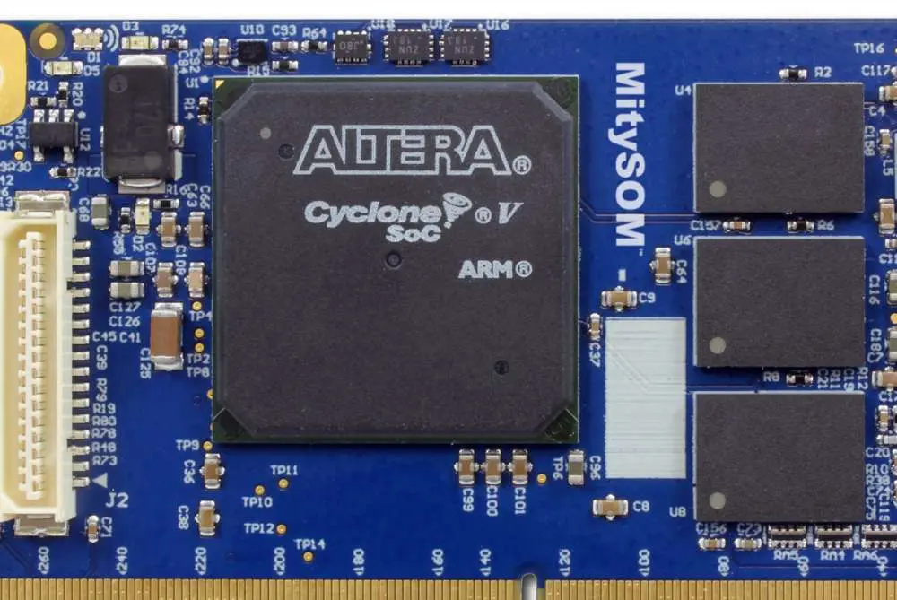
The Intel (Altera) Cyclone V FPGA family is one of the newest members of the Altera line-up. While this is the first time many people see these boards publicly, they have been in use for quite some time. This article will look at what makes this part special and why it might soon replace other parts of Altera‘s current line-up.
What is Altera Cyclone V
The Altera Cyclone V is a family of low-power field-programmable gate arrays (FPGAs) manufactured by Intel (formerly Altera Corporation). Introduced in 2010, Cyclone V FPGAs provide a balance of low power consumption, performance, and cost for mid-range applications such as industrial automation, automotive infotainment, and digital displays.
Some key features of the Cyclone V family include:
Low power consumption – Cyclone V FPGAs consume as little as 3 Watts static power thanks to Intels 40 nm process technology. This makes them suitable for battery-powered and green energy applications.
Performance – With a maximum frequency of 300 MHz, Cyclone V delivers up to 220K logic elements (LEs) and 96 Mbits of RAM to meet the needs of mid-range applications.
Cost-optimized – Pricing starts below $25 USD for high volume orders, providing an affordable option compared to higher cost FPGAs.
DSP blocks – Up to 220 18×18 multipliers allow for digital signal processing in applications like motor control and software-defined radio.
Multi-protocol communication – Support for protocols like Ethernet, USB, and PCIe allow for easy system connectivity.
Partial reconfiguration – The ability to reconfigure part of the FPGA while the rest remains active can help reduce power consumption.
This combination of features has made the Cyclone V series a popular choice for industrial, medical, automotive, and consumer applications that require low cost and power efficiency.
Cyclone V Architecture
Altera EP4CE15E22C8N
The Cyclone V architecture is built on a 40 nm process technology, which enables low static power consumption and a high logic density up to 220K LEs. The FPGA fabric consists of the following key components:
Logic Elements
The basic building block of Cyclone V FPGAs is the logic element (LE). Each LE consists of a 4-input look-up table (LUT) capable of implementing any 4-input logic function, along with a register to implement sequential logic. Cyclone V provides a abundant 120,000 to 220,000 LEs, allowing designers to synthesize complex logic functions.
Embedded Memory
Cyclone V provides approximately 10 Mbits of embedded memory blocks that can be used to implement FIFO buffers, RAM, and ROM functions within the FPGA fabric. Each device has between 160 to 594 M9K blocks, each block providing up to 9 Kbits of storage. For larger memory needs, Cyclone V also includes up to 16 Mbits of larger M144K blocks.
DSP Blocks
For digital signal processing functions, Cyclone V incorporates dedicated high-performance 9×9 multiply and accumulate DSP blocks. Each block can perform one 18×18 multiply accumulate operation per clock cycle. The larger devices in the family provide up to 220 of these DSP blocks.
Clock Management
Flexible clock management is critical for FPGAs, and Cyclone V provides up to 12 global clocks that can drive throughout the device. Each clock can be individually programmed for frequency synthesis, deskew, and dynamic phase shifting. There are also up to 88 low-skew routing clocks per device.
I/O
A wide variety of external interfaces can be implemented with Cyclone V I/O capabilities. Multi-voltage I/O banks support common standards like 3.3V LVTTL as well as 2.5V LVCMOS and 1.8V LVCMOS. High-speed inputs support data rates up to 1.6 Gbps. General purpose I/O provide flexibility for a wide range of applications.
Transceivers
For high-speed communications, selected Cyclone V variants incorporate up to four transceiver blocks. These multi-gigabit transceivers support data rates up to 6.5 Gbps for protocols like Ethernet, Fibre Channel, XAUI, and RapidIO. Each transceiver channel contains dedicated PLLs, clock data recovery, and channel alignment logic.
Configuration
Cyclone V can be configured using industry-standard methods like active/passive serial, JTAG, and AS configuration schemes. This allows the use of low-cost configuration devices and easy interfacing with common microprocessors. Partial reconfiguration is also supported for dynamically modifying sections of the FPGA while the rest continues operation.
Cyclone V FPGA Family
The Cyclone V family includes devices in four variants optimized for different applications:
E – Mainstream low cost FPGAs
GX – Transceiver variants with 2-4 transceiver channels
GT – High performance transceiver variants with 6-16 transceivers
SE – Lowest power optimized variants
Within each variant, different densities are available with different amounts of LEs, memory, DSP blocks, and transceivers. The following table summarizes the Cyclone V family specifications:
Device
LEs
M9K Blocks
M144K Blocks
18×18 DSPs
Transceivers
5CEA4
60K
241
4
66
0
5CEA7
110K
468
4
132
0
5CEBA4
85K
241
12
110
0
5CEFA4
120K
241
12
132
0
5CEFA7
150K
468
16
198
0
5CGXFC7
150K
468
16
198
2
5CGXFC9
220K
594
16
220
4
5CSEBA6
85K
241
12
110
0
5CSEMA4
60K
241
4
66
0
This range of densities allows designers to choose the optimal Cyclone V device to match their specific requirements. The highest density 5CGXFC9 provides a potent combination of logic, memory, DSP, and transceiver capability in a low power, cost-optimized package.
Cyclone V Development Kits
To simplify the design process, Intel provides a range of development boards and kits for Cyclone V FPGAs:
Terasic DE1-SoC – Features a Cyclone V 5CSEBA6U23I7N FPGA with 85K LEs, along with ARM Cortex-A9 processor and video interfaces.
Intel Cyclone V GX Starter Kit – Highlights the 5CGXFC9 transceiver capabilities with PCIe x4, SATA-II, and Gigabit Ethernet interfaces.
Intel Cyclone V SE Starter Kit – Demonstrates lowest power operation with the 5CSEMA5F31C6 FPGA variant.
Arrow SoCKit – Cost-optimized board with Cyclone V 5CSEBA6U23I7 FPGA SoC.
Using these kits, developers can start implementing and testing their designs with the Cyclone V hardware and software environment. The kits provide easy access to peripherals like memories, interfaces, switches, buttons, and displays. Many example designs and tutorials are available both from Intel and third parties to accelerate learning. Once a design is completed and tested, it can be migrated to a custom PCB for production.
Design Tools
To support Cyclone V developers, Intel provides a robust design environment:
Quartus Prime – FPGA design software with support all major HDLs like Verilog and VHDL. Includes logic synthesis, place and route, timing analysis, power optimization and simulation tools.
ModelSim – HDL simulator for verifying and debugging FPGA designs without hardware.
Nios II EDS – For developing embedded software for the Nios II softcore CPU that runs within the Cyclone V fabric.
Qsys – Tool for integrating intellectual property (IP) blocks into system-level designs.
DSP Builder – High-level block diagram tool for developing DSP systems with the Cyclone V DSP blocks.
This suite of tools provides everything needed for a complete FPGA design flow from conception through verification and debug. The tools support simulation, synthesis, place and route, timing analysis, power optimization and programming of the final bitstream.
Applications
With its combination of low power, performance and cost, the Cyclone V family targets a wide variety of applications including:
Industrial Automation – Programmable automation controllers, motor drives, robotics, and factory automation.
Automotive – Infotainment systems, driver assistance, camera processing, USB connectivity.
Consumer – Digital cameras, home automation, portable electronics.
Medical – Diagnostic systems, ultrasound, imaging, healthcare IoT.
Aerospace and Defense – Avionics systems, ruggedized electronics, radar processing.
Wireless Communications – 4G/LTE infrastructure, baseband processing, small cells.
For these applications, Cyclone V provides an optimal balance of capability and power efficiency in a cost-effective design. The low power eases thermal design while maintaining the performance needed.
Some specific customer examples include:
Glidecam – Portable camera stabilization system uses Cyclone V for control algorithms.
Nutaq – Software-defined radio platform built on Cyclone V FPGA.
Foxconn – High-volume manufacturing uses Cyclone V SoCs for quality control systems.
Comparison to Other FPGAs
Cyclone V is positioned between Intel’s low-cost Max 10 FPGA family and higher-end Arria series FPGAs in terms of price and performance:
Compared to competing mid-range FPGAs, Cyclone V differentiates with lower power consumption while maintaining high logic density and hard IP blocks for memory and DSP:
Overall, Cyclone V hits a sweet spot between the capabilities, power efficiency and cost structure desired by many mid-range applications.
Conclusion
In summary, the Cyclone V FPGA family provides an optimal balance of low power consumption, performance, and cost for mid-range applications. Key capabilities include:
Low power 40nm process technology.
Up to 220K LE programmable logic.
Embedded memory and DSP blocks.
Optional integrated multi-gigabit transceivers.
Mature design tools and IP ecosystem.
For industrial, automotive, consumer and communications markets needing energy efficiency and low cost, Cyclone V FPGAs are an excellent fit. With its high logic density, ample hard IP blocks, and aggressive power optimization, Cyclone V continues as a popular mid-range FPGA family.
Frequently Asked Questions
Here are some common questions about the Altera Cyclone V FPGA:
What process node is Cyclone V based on?
Cyclone V is manufactured on TSMC’s 40 nm low power CMOS process technology. This provides a good combination of density, performance and low static power.
What FPGA families are higher and lower than Cyclone V?
In Intel’s FPGA lineup, Cyclone V sits between the low cost Max 10 FPGAs and higher end Arria V FPGAs. Max 10 targets lowest cost while Arria V adds more performance and capabilities for high end applications.
What types of clock management blocks are in Cyclone V?
Cyclone V provides up to 12 global clocks that can drive throughout the FPGA. Each clock has individual clock control blocks with frequency synthesis, deskew, and dynamic reconfiguration. There are also up to 88 low-skew routing clocks per device.
How many I/O standards are supported by Cyclone V?
Cyclone V supports a wide range of I/O standards including 3.3V LVTTL, 2.5V LVCMOS, 1.8V LVCMOS, SSTL, HSTL, and differential standards. Multi-voltage I/Os allow interfacing to different voltage domains.
What configuration schemes can be used with Cyclone V?
Cyclone V supports active serial, passive serial, JTAG, and AS (fast passive parallel) configuration schemes. This allows low cost configuration solutions as well as processor-based configuration.
Cyclone V is available in all three of Altera’s technology nodes: Stratix 10 (10nm), Stratix 11 (16nm), and Stratix 12 (14nm). In the Stratix 10 technology node, this is at its smallest point. In addition, the Cyclone V adds 12-bit A/D converters, which is a new addition from the previous generation.
Stratix 11 and Stratix 12 have several differences between them in their Cyclone V offerings. Most notable is that Stratix 11 offers a 16-bit multiplier block with both add and divide functionality. On the other hand, Stratix 12 only offers a 16-bit multiplier block that does not have any add or divide functionality. Additionally, Stratix 12 offers a 16-bit multiplier block with only add functionality. But Stratix 11 offers both add and multiply functionality.
The other change is that Stratix 11 does not support on-chip memory while the other two do. However, since we know that this is due to the manufacturing of Stratix 11 on TSMC’s v10 60nm process while we make the other two on TSMC’s 10nm node, it is still unclear whether this is true.
The Cyclone V also differs from the previous Cyclone IV parts in that the memory interface is in a different location. They moved it off the FPGA chip itself and put on an L4 device called the C5N. This allows for better routing between FPGA companies.
The Cyclone V family has three different models, broken down by technology node, and these are 10LX, 10LX-S, and 10SS. The 10LX-S has a data rate of 60MHz, while the other two have a 40MHz data rate. Both have 16GB of onboard FLASH memory, while the C5N has up to 192GB of external memory.
The online documentation for this part is available at the CFE (Component Firmware Engine). The documentation includes a full pin-out of the part as well as device-specific information. It also includes a full description of the onboard memory built on a 10nm process. You can lock the FPGA from 100MHz to 400MHz, and the C5N from 100MHz to 400MHz
The latest version of Quartus II is Q2 2017 SP1, allowing Altera users to access Cyclone V within their systems.
Intel (Altera) Cyclone V FPGA Boards features
Features of the Intel (Altera) Cyclone V FPGA Boards include:
Cyclone V Architecture
36 customizable Digital Input/Output (I/O) blocks + 6 clock I/O blocks. The new Integrated Memory Controller (IMC) provides both on-chip and off-chip memories. It has 56-bit wide multipliers with multi-precision support.
Hardware FPGA Firmware for advanced security, intelligent routing, power management, and advanced programmable logic functions. Support for advanced bytewise programming operations such as Array Interleaving and Inline Operation.
Advanced tools for automated design and verification
Performance improvements on or above the previous generation
Cyclone V has more I/O pins than the rest of the Altera FPGA families. It allows for the combination of more FPGA devices. So there are no pluggable daughter boards. The board supports 8GB of onboard FLASH memory, which we can use as on-chip or off-chip memory.
Flexible Interface Support
Cyclone V has multiple options for interfacing to the C5N with speeds up to 10Gbps. There are four QSGMII transceivers, which are useful for gigabit ethernet. It also supports four SGMII transceivers used for serial communications protocols such as PCI Express Gen 2.
This FPGA has an integrated serial transceiver with multiple options for interfacing up to 10Gbps. Thus, it is useful for high-speed serial communication protocols such as PCI Express Gen 3.
Abundant Hard IP
There are over 120 IP blocks for easy integration of the Cyclone V into an application. The various Altera FPGA families have different IP blocks, but they are all available in Cyclone V.
Slice-based FPGA Architecture
Cyclone V slices its array into 64 slices. This means that the entire array is smaller than a regular FPGA part. But it still has all the functionality that Altera’s current FPGA chips provide.
Design Security
There is a hardware-based security mechanism, which we can use to prevent writing to data that may need erasing. This hardware protection is separate from the software control over who has access to the various bits within the FPGA.
The Cyclone V has a 128-bit hardware-based data integrity checker. It ensures that the part will output the same results as it would if you hand-programmed it manually. The checker uses a look-up table for this purpose.
Connectivity
The Cyclone V has an on-chip Ethernet controller with functionality for gigabit ethernet, 10GBase-T Ethernet, and PCI Express Gen 2. In addition, the serial transceiver supports SGMII, QSGMII, PCI Express Gen 2, and other serial interfaces.
A GPIO interface on the Cyclone V provides a standard set of inputs and outputs for connecting to other FPGAs. We can use this interface to connect to other chips with the right signals.
The Cyclone V also has a USB 3.1 controller that is capable of up to 20Gbps. We use eight FSMC USB controllers for wireless communication using protocols such as Bluetooth and Wi-Fi. The board also has two CAN controllers for communicating over CAN Bus networks.
Multiport Memory Controller
The on-chip memory has two ports, allowing it to interface with external memories using two different protocols. It allows for using the part in applications that require high-speed block-level access to external memory. So it makes it useful for cloud computing or scientific analysis applications.
Extended Power Management
The Cyclone V has extensive power management functionality. As a result it allows greater flexibility in system design. For example, it can alter its clock frequency based on current operating conditions. Also, it disables unused modules to control power consumption. It is compatible with the USB 3.1 SuperSpeed Plus standard for up to 20Gbps data transfer speeds.
Cyclone V also has “Embedded Debug Support.” It provides on-chip debugging functionality at low power consumption. We can use it to debug applications embedded in the FPGA, which is ideal for debugging.
Silicon and Architectural Optimizations
Several silicon and architectural optimizations are products of Cyclone V. These include a different set of memory control blocks. They allow the device to run faster and with less power. There is also a larger set of multipliers, which can optimize the FPGA’s performance.
10LX-S – The 10LX-S has a data rate of 60MHz while the other two have a 40MHz data rate.
Benefits of using Intel (Altera) Cyclone V FPGA Boards
The main advantages of using an Intel (Altera) Cyclone V FPGA Boards are as follows:
Tailored for High-Volume, Cost-Sensitive Applications
The Cyclone V is the lowest cost FPGA from Altera’s FPGA line-up. This makes it ideal for applications that need a large amount of I/O but don’t have a lot of space available to put the FPGA device. In addition, it includes applications such as networking and other large high-speed communications.
Flexible Integration Options
There are several options for integrating the Cyclone V into a system using Altera’s standard tools. There are four QSGMII transceivers, which we use for ethernet and other networking applications. We also use four SGMII transceivers for serial communications protocols such as PCIe Gen 2 and various network protocols.
Versatile Design
The Cyclone V has many different options for interfacing with other chips. There are four QSGMII transceivers, which we use for ethernet and other network applications. There is also a set of eight FSMC USB transceivers that are useful for USB 3.1 communication.
Tailored for High-Performance Designs
The Cyclone V has numerous performance features that allow its optimization for high-performance applications where the main limitation is the size of the FPGA part. The Cyclone V has a hardware-based checker, which makes it more secure. It runs at a higher speed than previous Altera FPGA parts. The Cyclone V also has larger multipliers. So, it allows the Cyclone V optimization for many different applications.
The Cyclone V is an ARM* processor-based FPGA that allows you to implement an ARM system on a single chip. It is a member of the Cyclone family. In other words, it provides a full set of FPGA blocks and IP for implementing most ARM processor functions. It includes the entire memory subsystem, I/O subsystem, and peripheral control. We can use the Cyclone V in an end-to-end design where we place it after the ARM core and before the rest of the SoC device.
Reducing Total System Cost through Integration
Cyclone V can reduce the cost of a system by replacing many discrete components in an SoC. They include the main processing core, memory, DSP, display controller, and other peripheral chips. This approach is attractive to leading companies such a RayMing PCB and Assembly that are looking for a way to reduce the total system cost.
End-to-End System Design
We can use the Cyclone V in an end-to-end design where it’s placed after the ARM core and before the rest of the SoC device. Other FPGAs provide all processing blocks required to implement an ARM SoC with all peripherals, memory, DSP, and I/O devices.
Industry-Leading Low Power and Low System Cost
Cyclone V uses the same high-performance architecture as other Altera FPGAs, such as the FLEX series. It has a 3.1V core voltage and runs at a 200MHz clock speed. The Cyclone V gives you many benefits of an all-FPGA design while also improving its performance. It uses advanced IP blocks in the FPGA, designed especially for low-power applications.
High-Bandwidth Interconnect
Cyclone V provides high bandwidth interconnects between the blocks within the FPGA. It is useful in applications where you need to transfer large data. Such data include image processing and other signal processing applications.
Cyclone V has four QSGMII transceivers used for data communication over ethernet networks, with data transfer speeds of up to 200Mbits/s. One can transfer data simultaneously, which is useful when reading or writing to flash memory in the FPGA.
ARM*-Based HPS
Cyclone V also has an HPS field-programmable gate array (HPS) block. ARM designed the block, but we can program it in the FPGA. The HPS is essential in off-chip applications by connecting the output of the QSGMII transceivers to an optional Cypress XC7K35P1. In addition, it provides a memory interface for ARM’s HPS.
Although the Cyclone V is a low-cost FPGA, it still offers many benefits that other FPGAs do not. The main drawbacks include:
The 1Gbit/s QSGMII transceivers, the FSMC USB transceivers, and the HPS are not available. So, you can’t use them to implement certain types of end-to-end designs.
There is no support for non-ARM systems. It includes AMD or ARM-based systems that one implements using a PCIe switch or other high-performance interfaces between the ARM core and the rest of the SoC.
Cyclone V doesn’t support DDR memory directly. However, it has a connector for using an optional XC7K35P1 memory device designed for use with the QSGMII transceivers and the HPS.
There is only one SGMII transceiver and one USB transceiver in the FPGA. You can’t add more of these transceivers to interface with more peripherals on an SoC design.
Although the Cyclone V has many drawbacks, it is still a very powerful FPGA that we can use in many different systems.
Intel (Altera) Cyclone V FPGA Boards applications
We optimize the Cyclone V for FPGA designs that use the ARM CPU. The following are some examples of systems that you can implement using Cyclone V:
1. Industrial networking, motor control
Industrial network systems are useful in many different environments. It includes factory automation, building automation, and mining. Cyclone V provides high-performance networking capabilities for industrial network systems. The QSGMII transceivers can connect the FPGA to the ethernet, which is essential for communication with other systems. Cyclone V can also implement motor control systems used within factory automation and building automation.
2. Wireless: Mobile backhaul, remote radio heads, picocell
Mobile backhaul systems are essential in cellular communication systems. It includes a wireless backhaul to the base station, which we connect to an ethernet switch. We can use Cyclone V to provide high-performance communication capabilities in these environments. The QSGMII transceivers are useful in data communication over the wireless network. But the FSMC transceivers are essential radio energy transmission or reception. Cyclone V can implement remote radio heads used in the field inside mines and other underground locations.
3. Wireline: Access routers, control plane
We can use Cyclone V in high-performance wireline routers that are useful in cellular networks. These routers are in the base station and connect the communications device to the network. The QSGMII transceivers can help data communication over the wireline network.
4. Broadcast: Capture cards, video conversion
The Cyclone V provides high performance for video conversion applications. It can help implement digital broadcast capture cards, which we use in analog broadcast television, satellite television, and IPTV systems. It can also convert analog low-definition television into digital high-definition television or other types of videos.
5. Cryptography
The Cyclone V is a secure processor that uses an ARM core for data processing. We can use it in applications that require high-performance encryption algorithms. You can use the HPS to provide an interface compatible with ARM’s processors, such as the Cortex-A8 and Cortex-A9.
6. Consumer: Displays
The Cyclone V is useful in consumer applications, such as digital TVs, home theater systems, and e-book readers. We can also use it in low-power embedded systems that include large displays.
7. Security
Affordable hardware security solutions are essential for secure communications between devices and networks today. The Arm Cortex-A8 is a highly integrated processor system used in many high-performance devices due to its high performance and low power consumption.
Cyclone V is a completely programmable system that we can customize to perform certain tasks in a system. The QSGMII transceivers help connect the FPGA to a high-performance network. We can use it in applications that require powerful processing capabilities, such as multimedia applications. The HPS is essential in applications where we need a memory interface with an ARM-based system.
ACM-027-A4 consist of the Altera 5CEBA4F23C8N FPGA with the following specifications:
100 Maximum user I/O pins (Board)
224 Maximum user I/O pins (Device
16 Global Clock Networks
4 PLLs
132 18 x 18 Multipliers
3,383 Kbits Embedded memory
49K Logic Elements
[ACM-027Z] Altera Cyclone V FPGA board
The ACM-027Z-A4 Is compact and straightforward, using a 3.3V power supply operation. The specification for the Altera 5CEBA4F23C8N FPGA includes:
100 Maximum user I/O pins (Board)
224 Maximum user I/O pins (Device)
16 Global Clock Networks
4 PLLs
132 18 x 18 Multipliers
3,383 Kbits Embedded memory
49K Logic Elements
[ACM-028] Altera Cyclone V F896 FPGA board
The ACM-028 consist of the Altera 5CEFA9F31C8N or 5CEFA7F31C8N. This FPGA Cyclone V board is straightforward and compact and offers high performance. Some of the specifications include:
5CEFA7F31C8N:
100 Maximum user I/O pins (Board)
480 Maximum user I/O pins (Device)
16 Global Clock Networks
7 PLLs
312 Embedded 18 x 18 Multipliers
7,696 Kbits Embedded memory
149.5 K Logic Elements
5CEFA9F31C8N:
100 Maximum user I/O pins (Board)
480 Maximum user I/O pins (Device)
16 Global Clock Networks
8 PLLs
684 Embedded 18 x 18 Multipliers
13,917 Kbits Embedded memory
301K Logic Elements
[ACM-109] Altera Cyclone V FPGA board
The Altera 5CEBA4U15C8N FPGA consists of the following attributes:
Like all the other Cyclone V boards made in Japan, it had High quality eight layers and a ten-pin socket JTAG Connector. The Altera 5CEBA4U15C8N FPGA has the following attributes:
56 Maximum user I/O pins (Board)
224 Maximum user I/O pins (Device)
16 Global Clock Networks
4 PLLs
3,383kb Total Memory
303kb MLAB Memory
3,080 kb M10K Memory
18,480 ALM
49K Logic Elements
132 18 x 18 Multipliers
[ACM-305Z] Altera Cyclone V FPGA board
This board is a Hi-performance FPGA Cyclone V board that is very simple and compact. The Altera 5CEBA4U15C8N FPGA has the following feature:
56 Maximum user I/O pins (Board)
224 Maximum user I/O pins (Device)
16 Global Clock Networks
4 PLLs
132 18 x 18 Multipliers
3,383 Total Memory
303kb MLAB Memory
3.080kb M10K Memory
18,480 ALM
49K Logic Elements
[AP68-07] Altera Cyclone V PLCC68 FPGA Module
With AP68-07, you will get 68pin PLCC FPGA that is simple and compact. The Altera 5CEBA4U15C8N has the following specification:
50 Maximum user I/O pins (Board)
224 Maximum user I/O pins (Device)
16 Global clock networks
4 PLLs
132 18 x 18 multipliers
3,383kb Total Memory
303kb MLAB Memory
3,080 kb M10K Memory
18,480 ALM
49K Logic Elements
[AP68-06Z] Altera Cyclone V PLCC68 FPGA Module
The Altera 5CEBA4U15C8N has the following features:
50 Maximum user I/O pins (Board)
224 Maximum user I/O pins (Device)
16 Global clock networks
4 PLLs
132 18 x 18 multipliers
3,383kb Total Memory
303bk MLAB Memory
3,080kb M10K Memory
18,480 ALM
49K Logic Elements
[EDA-008] Altera Cyclone V USB-FPGA board
Altera 5CEBA4F23C8N FPGA:
100 Maximum user I/O pins (Board)
224 Maximum user I/O pins (Device)
16 Global Clock Networks
4 PLLs
132 18 x 18 Multipliers
3,383KB Embedded memory
49K Logic Elements
[EDA-009] Altera Cyclone V USB-FPGA board, FTDI USB 3.0 FT600
The Cyclone V is the first FPGA Altera has produced that supports high-speed digital design. It allows for several high-speed applications. The 10SS can handle up to 60MHz of data, while the other two only support 40MHz.
From the above details, all variants support 16GB, 32GB, and 64GB of onboard memory. While this is not enormous compared to the typical DRAM found on modern systems, it will easily implement typical designs.
While there are limitations on the number of environmental effects allowed for this device, it does not appear to be much below what we find in modern FPGAs.
A transparent printed circuit board (PCB) is a specialized PCB that uses a clear insulating substrate material instead of the typical opaque FR-4 material. This allows building functional PCBs that are see-through, providing a unique aesthetic while still maintaining electrical functionality.
This article explores transparent PCB technology including:
Materials used and properties
Fabrication process
Applications and use cases
Advantages and limitations
Design considerations
Future trends
Understanding transparent PCB technology enables leveraging these visually appealing boards in products requiring high transparency like lighting, displays and other electronic assemblies.
Transparent PCB Materials
Conventional PCBs use opaque substrate materials like FR-4 which is a composite of fiberglass and resin. Transparent PCBs use clear insulating materials that allow light to pass through while still providing adequate dielectric insulation. Some options are:
Polycarbonate
An amorphous thermoplastic known for optical clarity and high impact resistance. Offers good temperature and chemical resistance. Used in riot shields, lenses.
PET (Polyethylene Terephthalate)
A crystalline thermoplastic polymer resin known for strength, thermal stability and transparency. Used in water bottles and food containers.
PMMA (Polymethyl Methacrylate)
An amorphous thermoplastic known as acrylic glass. Provides high light transmittance. Used in aquariums, aircraft windows.
Glass Reinforced Epoxy
Composite of glass fabric and epoxy known for dimensional stability. Provides very high optical clarity along with rigidity.
LCP (Liquid Crystal Polymer)
A highly chemically resistant crystalline thermoplastic polymer allowing thin and flexible PCBs.
These transparent insulating materials enable fabrication of PCBs that are see-through while still providing adequate dielectric insulation for proper functioning of the circuits.
Any application where both lighting effects and electronic circuitry need to co-exist in a single assembly can potentially benefit from transparent PCB technology.
Some emerging trends shaping transparent PCB technology are:
Materials R&D
Developing new transparent substrate materials with enhanced capabilities
Manufacturing Improvements
Innovations enabling higher layer count boards with smaller vias
Touch Integration
Embedding touch sensors within transparent boards
Flexibilization
Creating flexible transparent circuits
Additive Processing
Leveraging additive methods like inkjet printing of conductors
Miniaturization
Producing transparent circuits on thinner substrates for compact products
Design Automation
CAD tools optimizing layouts for transparent PCB needs
Smart Lighting
Integrating transparent electronics into smart LED lighting
New Applications
Adoption in emerging industries like wearables, EV, AR/VR
Continued progress in materials, processes and design tools will expand applications for transparent PCB technology across industries where aesthetic lighting and electronic functions need merging in novel ways.
Conclusion
Transparent printed circuit boards enable illuminating creativity in product design by merging lighting aesthetics and electronic functions using clear insulating substrates. With its unique set of advantages and widening range of applications across automotive, consumer products, medical devices and industrial automation, transparent PCB technology empowers products to blend electronics seamlessly into visually appealing illuminated structures. As manufacturing processes and new substrate materials advance, transparent PCBs hold the promise to transform future electronic product paradigms in stunning ways.
What is a Transparent PCB? – FQA
Q1. What materials are used to fabricate transparent PCBs?
Transparent PCB materials include polycarbonate, PET, PMMA, glass reinforced epoxy, liquid crystal polymers which provide optical clarity along with adequate dielectric insulation.
Q2. What kind of applications use transparent PCB technology?
Applications include LED lighting, automotive tail lights, consumer appliances, medical dialysis machines, industrial HMI, interactive public kiosks needing electronic-lighting merging.
Q3. What are some advantages of using transparent PCBs?
Benefits include aesthetic appeal, light transmission, component illumination and visibility, improved thermal dissipation, reduced EMI through non-metallic enclosure.
Q4. What are some limitations and challenges with transparent PCBs?
Limitations are higher cost, smaller sizes, lower thickness, component visibility contrast, safety standards, assembly complexity, electrical resistance and debug difficulty.
Q5. What are some future trends shaping transparent PCB technology?
Trends are new substrate materials, manufacturing improvements for higher layer counts, touch integration, flex circuits, additive printing, design automation tools and applications in lighting, wearables and AR/VR.
The Intel MAX 10 is a low-cost, instant-on, non-volatile field programmable gate array (FPGA) by Intel (formerly Altera) aimed at a wide range of industrial IoT, embedded vision and compute applications.
This article provides an overview of the Intel MAX 10 architecture, features, design considerations, available options and target applications to help designers evaluate its capabilities.
Intel MAX 10 Architecture
The MAX 10 architecture is built on Intel’s 14nm process and consists of the following key components:
Logic Fabric
Based on Intel’s Adaptive Logic Module providing optimal balance of logic, memory and DSP resources
Up to 50K LEs (logic elements) providing over 300K logic cells
LABs (logic array blocks) with 10 LEs each, carry chains, registers
Peripheral sets for interfacing, communications, computing
Non-volatile Configuration
Unique flash memory based configuration unlike SRAM FPGAs
Instant boot up, low power retention during shutdown
This combination of flexible programmable fabric along with abundant hardened blocks for common functions enables creating a wide range of embedded and industrial electronic systems using the MAX 10 FPGAs.
Some of the major highlights of Intel MAX 10 devices are:
Low Cost
Aggressively priced for high volume markets
Lowest cost programmable logic solution
Small Form Factor
Compact fine-pitch packages including CSP/BGA options
Power Efficiency
Typical static power under 100 mW
Hibernate power mode for μW retention
Non-Volatile Operation
No external configuration memory needed
Instant power on with flash-based configuration
Mixed-Voltage Support
1.2V core with 3.3V I/O supply
Robust Security
AES-GCM 256-bit encryption blocks
Pubkey authentication, access prevention
SEU Immunity
Resistant to radiation induced errors
-40°C to +125°C Operation
With its compelling combination of low-cost, low-power, mixed-voltage operation, reliability and abundant hardened blocks, the MAX 10 brings new flexibility and capabilities compared to CPLD or microcontroller solutions for embedded systems.
Intel MAX 10 Design Considerations
Key aspects designers should keep in mind while working with the MAX 10 FPGA:
Use power analysis tools to optimize current consumption
Thermal Design
Employ proper heat sinking for high power variants
Security
Make use of robust built-in security capabilities
Team Skills
Prior experience with Intel/Altera FPGAs is beneficial
Considering these aspects early in the design cycle helps harness the full potential of MAX 10 devices.
Intel MAX 10 Options
The Intel MAX 10 is available in a range of variants with different I/O counts, logic, memory and DSP resources to match diverse application needs:
Device
Logic Elements
Embedded Memory
Transceivers
GPIO
Packages
MAX10M02 C2
2000 LEs
1.1 Mb
0
32
24-pin CSP
MAX10M04 C4
4000 LEs
1.9 Mb
0
60
36-pin CSP
MAX10M08 C8
8000 LEs
2.2 Mb
0
114
48-pin CSP
MAX10M16 C16
16000 LEs
3.3 Mb
0
158
64-pin CSP
MAX10M25 C25
25000 LEs
3.3 Mb
0
158
64-pin CSP
MAX10M50 C50
50000 LEs
5.5 Mb
4
158/240
84-pin CSP/F1517
This scalable portfolio allows developers to choose the optimal device configuration matching embedded system needs in terms of I/O, logic resources, memory and cost.
Target Applications
With its compelling blend of low-power, reliability, small form factor and real-time performance, MAX 10 FPGAs are well suited for a diverse set of industrial applications:
Embedded machine vision – Vision sensors, inspection systems
Industrial automation – Motor drives, robotics, PLC expansion
Aerospace and defense – Vehicles, communications, munitions
Communication systems – 5G, wired broadband, MANETs
Medical – Diagnostics, imaging, prosthetics
Video and imaging – Surveillance, traffic systems, video codecs
Edge computing – Networking gear, gateway systems
Automotive – Body electronics, in-vehicle communications
Energy infrastructure – Smart grid, power equipment
The non-volatile flash-based configuration enables reliable instant-on edge computing systems in harsh operating environments. MAX 10 provides a flexible alternative compared to custom ASIC implementations.
The enhancements make the MAX 10 suitable for more complex embedded systems compared to MAX5 devices.
Conclusion
The Intel MAX 10 is an extremely flexible low-power FPGA family that provides an optimal combination of programmable logic, hardened blocks and I/O tailored for edge computing, embedded vision, industrial and communication systems.
Leveraging Intel’s mature design tools and a rich ecosystem of proven IP enables rapid development of robust products. The non-volatile flash-based configuration offers reliable instant-on performance for industrial deployments.
With its aggressively priced and scalable portfolio, the Intel MAX 10 offers compelling capabilities as a replacement for CPLDs, microcontrollers and ASICs across a diverse range of embedded applications demanding real-time intelligence and connectivity at the edge.
What is Intel MAX 10 FPGA? – FQA
Q1. What applications is the Intel MAX 10 FPGA suited for?
The MAX 10 with its low cost, low power, reliability and small form factor is ideal for industrial automation, embedded vision, aerospace, medical, imaging, edge computing systems.
Q2. How does the MAX 10 architecture differ from SRAM-based FPGAs?
MAX 10 uses flash memory for non-volatile configuration unlike SRAM FPGAs that need external flash at power up. This enables instant on capability.
Q3. What are some key components in the Intel MAX 10 FPGA?
Key components are the 14nm low-power logic fabric using ALMs, ample embedded memory blocks, variable precision DSP blocks, clock management, transceivers and rich Intel FPGA IP.
Q4. What are some benefits of the MAX 10 FPGA?
Benefits include low cost, power efficiency, compact footprint, robustness, reliability through radiation immunity, mixed voltage operation, built-in security and abundant hardened blocks.
Q5. How does MAX 10 improve upon Intel’s prior MAX5 FPGA generation?
MAX 10 enhances the MAX5 with up to 10X higher density, addition of hard transceivers, higher speed grade options, more memory blocks, reliability through SEU immunity and lower power consumption.
PCB insulation involves the use of dielectric materials to separate and protect the conductive layers of a circuit board. As electronic devices often generate high temperatures, proper insulation is essential to maintain performance and reliability. PCB manufacturers utilize dielectric materials to ensure that the board’s components remain isolated and secure.
Key reasons for insulating printed circuit boards include:
Maintaining adhesion at operating temperatures
Reducing signal interference between layers
Preserving voltage integrity and signal quality
Supporting effective thermal management during production
Insulation plays a critical role in ensuring the durability and functionality of PCBs in various applications.
PCB Insulation Materials
Different PCB applications require specific insulating materials. Here’s an overview of common types:
Thin, solid coating that doesn’t restrict movement
Often applied as a PCB insulation spray
FR-2 (Flame Resistant 2):
Combination of plastic and paper
Lighter than FR-4, best for single-layer PCBs
Less fire-resistant but durable and water-repellent
Used in inexpensive electronics due to lower cost
Radio Frequency Coating:
Specialized for devices using radio frequencies
Ideal for aerospace and in-flight electronics
Effectively manages high frequencies
Choosing the right insulation material is crucial for ensuring optimal PCB performance and longevity in specific applications.
How does the insulation aid PCB design and operation?
PCB Insulation Hole
In recent times, most PCBs come in multiple layers. This is due to technological advancements. The doubled and many layered PCBs are more solid with high speed, thick with more components on the board. These advantages are with complexities that include signal routing.
To deal with these hitches, a perfect choice of PCB insulation that manages the layers is vital. The selection procedures for consideration are as follows:
Temperature Progression/Movement
The impact made by high temperature on the board during production is a key factor to ponder about. A flexible PCB design needs many movements as against the woody PCB design.
Board Classification
The insulating material that fits the majority of the classification of PCBs is the FR -4. However, interruption caused by the control placed on PCBs with high speed is a factor to look into. This requires that insulation should be high enough to defy such interruptions.
Insulation density and signal layers
Another major factor to consider in selecting insulation for PCBs is its thickness. If a thin insulation is the choice, the base insulator beside the signal layer might disconnect. This disconnection between the signal layers will reduce the electromagnetic interference. Even so, choosing a thicker insulator on a double signal layer will allow routing on the next layer.
The Height of the PCB
The depth of the PCB can be a restraining factor to the elevation of the insulation in the design. In as much as size plays a major role in the usage of multiple layered PCBs.
A freshly produced PCB comes with the expectation of perfect performance. As well as the projection that all components of the PCBs are well suited for work without itches.
Nonetheless, the PCB is open to mitigating factors that could hamper its efficiency. Environmental variables such as corrosion, dust, temperature and dirt could affect the PCB. Also factors such as voltage surge, overburden voltage and accidental impact could mitigate.
The durability and integrity of the PCB could be reduced as a result of these demeaning factors. As such, manufacturers adopted the PCB insulation coating to remove these negative factors.
The insulation coating provides coverage for the PCB against all environmental variables. It is suitable for use in a broad range of environments to protect the PCB from all kinds of mitigating factors.
The coverage provided by the insulation coating enhances higher current incline. Thus, producers are able to match the compactness and integrity demands by end users.
Define PCB Insulation Coating
Insulation coating means the method of applying resistant materials to the PCB layer. This can either be through brushing, dipping or spraying of the coating material on the PCB. Thus, the PCB is well protected against destruction caused by tough environments.
Furthermore, the PCB insulation coating also enhances the stoppage of electrical discharge. Insulation coating increases the lifespan of the PCB. Mechanical and heat pressure, damages during installation and brutal handling are practically eliminated.
Composition of PCB insulation coating materials
For a PCB insulation coating to serve as a perfect coverage to the PCB, some attributes are salient. These attributes are exceptional electrical conduction, good temperature properties, chemical inertness and absorption.
Furthermore, insulation coating will enhance the resistant capacity of PCBs against environmental variables. As well as increasing the lifespan of the PCBs.
The insulation coating materials are basically divided into five categories. They are epoxy resin, polyurethane, organic silicon, parylene and acrylic acid resin. This is due to various contributing elements that make up the coating materials.
Categories of Insulation Coating Materials
Epoxy Resin Coating
This type of PCB coating is routinely applied on the PCB. This is due to its components and characteristics. Epoxy resin coating has high corrosion, moisture, and is temperature-resistant. It also has an exceptional permanency strength.
Equally, epoxy resin sprayed PCB is prone to a bad performance in cold environments and it shrinks. Alteration is difficult on a PCB with epoxy resin except if it is stripped physically. Thus, damage to its components as well as excessive inner distress to frail devices will occur.
Polyurethane Coating
This insulating coating can be solidly stiff, humidity sensitive and hard to take off. Yet, it is highly durable, defies mugginess and it is resistant to acid and soluble. Polyurethane is suitable for a broad range of applications.
Due to its solid nature, rectifying any defect on a PCB coated with polyurethane is tough. The process of curing takes a lot of time which might change its face color to yellow at high heat conditions. Also, it might likely stimulate screw ravaging.
Organic Silicon Coating
The PCB insulation coating made up of organic silicon is best suitable for high circuit PCBs. This is due to its numerous dominant resistors. It is pliable and it provides an admirable resistance to moisture and heat.
Although the silicon remnants on the PCB are hard to detach, it is poor at sustaining mechanical stability as well as resisting corrosion.
Parylene Coating
Parylene coating is a unique preservative coating used in the electronic industry. It breaks the organic compound in the vacuum valve and lays the coating evenly on the surface of the product.
More so, the parylene coating is the most efficient for highly compatible devices. It also serves as the best suited for high frequency PCBs as it provides total cover, it is also stout and thin.
Nonetheless, parylene coating is costly which stands as the only disadvantage to its choice.
Acrylic Acid Resin coating
This type of insulation coating favors electrical devices. Modification on this insulation coating is simple and it is relatively cheap.
Furthermore, the acrylic insulation coating possesses a very good moisture resistant ability. Also it has a flexible density adaptation and dries quickly.
Fixing a PCB coated with this type of insulation is technologically simple. The process is dependent on the evaporation of the soluble.
Insulation is as important to the circuit board as housing is important to human lives. Insulation serves as the shield against likely attacks on the PCBs.
Circuit board insulation is the use of non conductive materials to detach the layer from conducting components on the circuit board.
The contributory role of the circuit board is quite significant. Its existence has made the operation of electronic gadgets very effective. The circuit board consists of integrated components to allow perfect functionality. These include the transistors, the inductors as well as resistors, capacitors and Diodes.
Understanding of the board’s fabrication and its automated attributes is important. This is to make sure its production is of the best quality, thus best operation of the circuit board.
PCBs get descriptions in accordance to the number of layers they have. Nonetheless, during the pile up system, decisions on various parameters come to fore. They include insulation surface, their setting and kind of materials
Furthermore, taking a precise decision depends on the knowledge the producer has. The factors to consider are physical, electrical, temperature and mechanical properties. In order to take right decisions, the under listed objectives will be a guidance
Aim of PCB insulation among layers
Insulation aids veracity and signal
Reduction or getting rid of signal interruption among the layers
Sustain gluing during temperature inversion
Conclusion
PCB insulation is an aspect of the manufacturing process that is very crucial. Insulating your PCBs promotes durability, integrity and safety of the PCB. PCB being the bedrock foundation on which the majority of electronic gadgets thrive lately; sustaining the growth of the industry should be a priority.
Printed circuit boards have continued to be the core of most electronic devices. The manufacturing of these boards requires some steps. The PCB slot is a vital aspect of the PCB design. Manufacturers must understand the PCB slot before commencing on any device.
The presence of slots in a circuit board has several benefits. The effect of slots in circuit boards can’t be underestimated. PCB slots are available in different types. Therefore, it is important to have detailed knowledge about these slots.
What is a PCB Slot?
A PCB slot is a hole in the circuit board that is too big to be formed by normal drilling methods. Manufacturers need to cut out these holes with a routing bit during the fabrication of the PCB. A slot PCB can either be non-plated or plated.
The two major types of PCB slots are the plated slot and non-plated slot.
Plated slot
In PCB manufacturing, a plated slot has copper plating. The plated slot is the type that has no circular shape. A PCB slot that features copper on the bottom and top is a plated one. This type of slot is ideal for electrical connections. Plated through hole slots are ideal for component packaging. Multilayer PCB always feature this type of PCB slot.
In PCB manufacturing, there are several component types for circuit boards assembly. The majority of through-hole part outlines feature round holes to take square or round leads. Most through-hole assemblies match this configuration. However, several parts use rectangular leads that don’t fit into square or round holes. Therefore, a plated slot is a better option.
Big blade-style connectors should incorporate plate through slots as the pins’ size increases. When the parts are small, manufacturers can make use of round holes featuring rectangular pins. However, round holes use up more space on the circuit board. Plated slots are more ideal for size-constrained designs.
Non plated slot
The non plated slot features a hole bigger than the pad’s copper size. Sometimes, there might be no copper. In a non-plated slot, the copper of the pad overlays. The manufacturer drills the non-plated slot after the electroless copper process.
slot pcb
Defining PCB Slot on Circuit Boards
If you are including slots in your PCB design, it is better to put them in Gerber mechanical layer. This layer is the safest way that shows the slots and the profile of the circuit board. There are two ways to do this:
Use flashes or draws featuring the right end size of the slot
Use a 0.50mm line to draw the slots. The line helps to analyze the clearance of the copper to the circuit board edge.
You can combine the slots’ definition with the PCB contour into the Gerber file. The mechanical layer must be with the copper layers. However, ensure the copper layer also features the PCB outline. If no mechanical layer is available, you may have to use another layer.
Don’t define slots in a legend layer or copper layer only. This is because they are easy to misunderstand. Indicate large cut-outs in a legend or copper layer. However, ensure you put a clear outline. Also, it is very important you indicate the slots in a README file. Do this when you are skeptical about the right one.
Some CAD systems enable PCB manufacturers to define slots in the drill file. However, the manufacturer must define the slots using an X and Y dimension. The X and Y dimension refers to slot width and slot length respectively.
The smallest width for a slot of rigid-flex and flex circuit is 0.50mm. While the smallest length for a slot is 1.0mm. This is because of the thickness of a rigid-flex and rigid PCB. Therefore, the mechanical NC milling should create the slots. The thicknesses of a flex circuit are thin. So, a laser can cut these slots.
If the length of a slot is longer, the slot will be straighter in length. Note that, the smallest length of a slot is 2 times of the width of the slot. For instance, if the width of a slot is 0.60mm, the length of the slot will be 1.20mm.
Slots Milling
The manufacturer mills out the slots from the rigid PCB material. Then, the PCB fabrication makes use of a NC grooving cutter bit. This cutter functions like a CNC machine. Also, the cutouts’ inside corners will feature a round edge to them. Make sure you keep an eye on this in enclosure designs.
The smallest radius for inside corner is 0.50mm. The smallest tool for routing out circuit boards is 1.0mm. Milling slots create air gaps for voltage isolation on the circuit board.
How to Use Eagle to Create Slot PCB
You might wonder if it is possible to create slots in Eagle. Slotted holes are popular in PCBs since components need to manipulate rising current. Many components feature wide pins. This is because a wide pin provides a component with more mechanical integrity.
Manufacturers can create slot PCB. It is important to use a through hole pad that has a diameter that fits your slot. An ideal pad for this operation is Oblong pad.
Draw the slots
Draw the slot outlines to draw your slotted holes. You can do this in a different way. Using the dimension layer is a great way to do this. However, this method has its limitation. The autorouter can’t get to the inside of the pad. Thus, there will be some dimension errors.
Ensure you set the pad’s drill size to fit within the slot PCB outline. This will help prevent any confusion and ensure a better result. The PCB manufacturer will mill the area within the outline from the board.
Get mill data to board manufacturer
Ensure you export a Gerber file to your manufacturer. While exporting the file, include a note. This note will specify that the manufacturer must mill the contents on the Gerber file from the board.
Defining Plated and Non-plated Slots in PCB design
The PCB fabrication process involves etching a copper sheet. This sheet is then plated on a substrate and holes are drilled on it. Before the plating process, these slots are non-conductive. Manufacturers use the electroless deposition process for PCBs with over one copper layer.
However, designers must know that not every slot will need plating. Therefore, designers need to abide by the rules of manufacturers to know which slot will be plated. Sometimes, designers expect some features in the circuit boards. However, they get an entirely different board in the end. Mounting slots are examples of such.
For instance, there will be issues if your design depends on a certain slot being plated. Unfortunately, you realize that the slot hasn’t been after receiving the board. Therefore, we will point out the difference between plated slots and non-plated slots.
How to consider a slot as plated
Before a slot is considered plated, it must meet certain conditions. Otherwise, it is a non-plated slot. In a plated slot, the copper of the pad alongside the solder stop mask must overlay. The pad’s copper must be more than the slot with at least 6 mil in width.
How to consider a slot as non-plated
Sometimes, some PCB slots are non-plated due to a mechanical or electrical reason. Any slot that features properties that don’t meet the plated slot conditions is a non plated slot. A slot PCB is non-plated, when the hole is bigger than the pad’s copper size. Furthermore, when the copper of the pad overlays and is bigger than the hole. However, there is a space clearance of 6 mil between the hole and the copper. Such conditions meet the requirements of a non-plated slot.
Applications of Non-plated and Plated Slots
Slots and Cutouts PCB
Milling slots create air gaps for isolation of voltage on circuit boards
There can be temporary electrical arcs between traces in a circuit board featuring high voltages. Repetition of electrical arcs can result in PCB carbonation. This can cause a short circuit in the long run. As a result of this, PCB designers include a milling PCB slot between suspect traces.
Plated slots are ideal for parts featuring square or rectangular leads
These slots fit in for parts with square/ rectangular leads rather than the rounded ones. The footprint for slots is better than for large holes. This is because the space between the wall of the hole and the lead must contain enough solder.
For a PCB assembly, there are several component types and footprints. Designers use circular holes to design most through-hole part footprints. This is because the circular holes can accommodate square or round leads. This is an ideal configuration for through-hole components. However, many parts use rectangular leads. These leads don’t fit into square or round holes. It is better to incorporate a plated slot footprint.
When the footprint leaves more space around the component leads, the circular hole configuration will be vulnerable to some defects. This can lead to solder joint voiding. This type of defect occurs when more solder fills the holes. Manufacturers become more concerned as the pins’ size increases. Therefore, large rectangular connectors should incorporate plated slots instead of circular holes.
Some manufacturers can work around circular holes for rectangular pins. Also, the circular holes end up taking more space on the circuit board itself. Using big circular holes is not ideal for layout demanding dense component populations. Incorporating plated slots can provide solutions in size-restricted designs.
PCB designers need to consider a few things while designing non-circular holes. However, the design process of non-circular holes is straightforward. Plated slots are commonly utilized in component footprints. Most programs for PCB layout feature an option to define a hole as oval or circular. In addition, some clients identify slot holes on the design layer of their Gerber files.
Designers can also design non-plated slot PCB in a similar way. They can then designate it as Mechanical or NPTH in the CAD software. They can also design them on the Board Outline Gerber layer. It is important that manufacturers pay attention to the design rules of PCB slot.
Designers need to define some things in the EDA tools to create plated slots. Most EDA tools allow designers to create plated slots through a manual process. Here, the designer identifies all the aspects of the hole rather than placing a standard pad. The three most important factors to consider when creating a plated slot are;
The shape of the hole
The copper’s shape on the top layer
The copper’s shape on the bottom layer
Plated slots differ from other holes in PCB designs. This is because they are drawn on the board outline layer. When PCB manufacturers receive manufacturing files, they interpret the board outline as cutting information. The manufacturer will route the board inside the already drawn shape. This will be done if there is a shape on the board outline layer.
A drawn hole inside the pads on the bottom and top of a PCB is interpreted as a plated slot. Therefore, designers need to draw the intended holes in the footprint on the board outline layer. The slot will display in the board outline file when producing the manufacturing files. Plated slots enable designers to make use of parts with non-circular pins and leads.
Frequently Asked Questions
What is the size of the plated slot on PCB?
0.5mm is the minimum size for a plated slot. If manufacturers realize the through-plating within the PCB, it is a plated-through slot. While through-plating on the outer edge of the PCB is sideplating.
What is the benefit of a PCB slot?
A PCB slot helps to connect the circuit board to other PCBs. It also helps to connect the board to the chassis of a device.
Can slot PCB increase the price of the overall circuit board?
No, slots in a PCB will not increase the price of the overall board. It will not also increase the lead time of your project.
Conclusion
Slot PCB is a vital aspect in PCB design. It is very important to understand how these slots work in PCB designs. The plated and non-plated slots have their function. However, plated slots are more popular in the PCB industry.
A Gerber file viewer refers to software tools that allow viewing and analyzing Gerber files containing 2D CAD data describing printed circuit board (PCB) designs. Online Gerber viewers provide the capability to upload Gerber files and visualize PCB designs within web browsers without needing to install any software.
This article covers:
Gerber file format overview
Need for online viewers
Features and capabilities
Benefits of online tools
Top online Gerber viewers list
Using online viewers effectively
Limitations to consider
The future of online tools
Understanding online Gerber file viewers enables PCB designers to efficiently inspect designs, communicate with manufacturers and speed up prototyping iterations.
Gerber File Format
Gerber files are the standard file format used to transfer PCB design data between CAD software and PCB manufacturing equipment like photoplotters. Some key points:
Gerber files are exported layer-wise from PCB design software like Altium Designer or KiCad before manufacturing. Each layer describes a unique aspect of the PCB design data.
Sharing PCB designs with manufacturing partners worldwide requires sharing large Gerber files containing the intricate board details. However, transferring and then viewing these files on local CAD software is cumbersome. Online Gerber viewers provide a quick and easy way to visualize the design and collaborate by:
Allowing uploads of zipped Gerber folders or individual files
Rendering 2D previews of the PCB instantly
Enabling sharing accessible links with the hosted view
Visualizing from any device without software downloads
Inspecting specifics with pan/zoom capabilities
This makes online viewers indispensable tools for PCB designers aiming to speed up design reviews, manufacturing discussions and prototyping iterations.
Features of Online Gerber Viewers
Online Gerber viewers offer a suite of features for comprehensive PCB visualization and inspection:
The range of analysis, inspection and collaboration features offered make online tools invaluable for optimizing PCB designs before manufacturing.
Benefits of Online Gerber Viewers
Gerber Files
Online Gerber viewers provide powerful advantages:
Easy Sharing
Hosted views allow sharing PCB design details with anyone instantly
Accessibility
View designs and collaborate from anywhere through browsers
Ease of Use
No need to install complex PCB software locally
Time Savings
Significantly faster design reviews and vendor discussions
Enhanced Visualization
Zoom into finest routing details for clarity
Team Collaboration
Annotate and share feedback on hosted views
Manufacturing Insights
Get assembly feedback from manufacturer teams
Cost Reduction
Avoid multiple PCB design iterations and corrections
Design Validation
Thoroughly inspect designs prior to fabrication
By facilitating instant PCB visualization and feedback online without software hassles, significant time and cost savings can be achieved during product development.
Top Online Gerber Viewers
Many free and paid online Gerber viewers provide capabilities for PCB inspection. The most popular choices are:
Gerber-Viewer.com
Free online viewer with basic PCB viewing features
Good rendering but lacks advanced capabilities
ViewMate
Basic layer viewing along with annotations
Limited collaboration features
JustGerb.com
Free online tool with good visualization
Email sharing and simple measurement
Tracespace Viewer
Advanced 3D rendering engine built on WebGL
Capabilities like DRC, BOM, step-and-repeat
CircuitHub
Feature-rich online viewer integrated with PCB services marketplace
Design reviews, quotes, orders managed through platform
Despite immense capabilities, online Gerber viewers also have certain limitations:
Lack advanced PCB editor features only available in full desktop CAD tools
May not render some component 3D models or pad shapes accurately
DRC checks may not be as exhaustive as desktop tools
Annotation capabilities are limited compared to design software
Can handle moderate sized designs but very large boards can get slow
Proprietary data not fully secured compared to local viewers
Require active internet connection unlike standalone tools
Online tools complement but cannot fully replace advanced desktop PCB design software yet. Secure data transfers and downloads are recommended for proprietary designs.
The Future of Online Gerber Viewers
Online Gerber viewers are expected to evolve with:
Enhanced Real-time Collaboration – Allow multiple stakeholders to visualize and annotate PCB designs seamlessly in real-time.
Augmented Previews – Offer augmented layer previews combining 2D, 3D and x-ray views for enhanced visualization.
Design Editing – Move beyond just visualization to limited PCB editing capabilities.
Deeper CAD Integration – Tighter integration with popular PCB design tools for seamless workflows.
Advanced DRC – Faster and more sophisticated design rule and electrical checking algorithms.
BOM Integration – Intelligent data extraction to build component lists and Bom directly online.
Manufacturing Integration – Close integration with manufacturing through ordering and production tracking.
Scalability – Ability to handle larger designs, higher data volumes as internet speeds increase.
As online tools gain more sophisticated capabilities, they are poised to become integral hubs connecting PCB design, analysis, collaboration, manufacturing and production workflows in the future.
Conclusion
Online Gerber viewers provide a quick and easy way to visualize, inspect and collaborate on PCB designs through an accessible online platform. They fill a vital need in electronics product development by facilitating rapid design reviews, discussions with manufacturers and speeding up iterations required before finalizing board fabrication. While lacking advanced editing features of full desktop tools, online viewers in their current form complement design software through key capabilities like multi-layer previews, annotations, measurements, screenshots and online sharing. With continual improvements in real-time collaboration, augmented views, design rule checking and deeper integration with PCB CAD, online Gerber viewers hold immense potential to enhance and integrate the electronics development workflow.
What is Online Gerber File Viewer? – FQA
Q1. What file format do Gerber viewers allow inspecting online?
Gerber viewers enable viewing Gerber files – the standard file format for transferring PCB design data to manufacturing containing 2D CAD information of the board.
Q2. What are the key advantages of online Gerber viewers?
Benefits include easy online sharing, accessibility through browsers, quicker design reviews and collaboration, rapid iterations and avoiding multiple board fabrication cycles.
Q3. What are some examples of popular online Gerber viewers?
Top online Gerber viewers are Gerber-Viewer.com, ViewMate, JustGerb.com, Tracespace Viewer, CircuitHub Viewer, Altium 365 Viewer and PCBWeb Viewer.
Q4. What are some limitations of online Gerber file viewers?
Limitations are lack of full editing features in desktop tools, inability to handle very large designs, lower data security than local viewers and need for active internet connection.
Q5. What future improvements are expected in online Gerber viewers?
You can open the PCB online Gerber file viewer with PCB editor software in two modes: online or offline.
In online mode, you can open the software directly from the PCB editor software. The two are running at in same time. You can use them independently or each other for cross-checking purposes. For example, you can view the Gerber file in PCB editor software, change some information and then switch to online Gerber viewer to review how it affects the Gerber file. You can also check how your layout looks like after printing it out. Or you can do all three at the same time. You can save the layout to an external file (it is handy if you need to modify/edit it in another software) and then reload it to PCB editor software.
You must open the Gerber file with PCB editor software offline, then open the online Gerber viewer application separately. We use them independently, but no communication between them. Once you complete your layout in the PCB editor software, you can save it in Gerber file format. Then launch the online Gerber viewer application to view and check your layout in the Gerber file. It is also handy if you need to modify/edit it in some other software.
The following sections will show you how to use both modes, step by step.
Online Gerber Viewer
Step 1: open PCB online Gerber viewer with PCB editor software
(1) Online mode:
Launch the PCB editor software you are using and load a Gerber file to open the layout
Go to view>More>Online Gerber Viewer, click it to launch it
The system will display the layout in the online Gerber viewer
(2) Offline mode:
Launch the PCB editor software you are using and load a Gerber file to open the layout
Optional: use the Plus icon to create a new folder and name it as you like
The system will display the in the online Gerber viewer
(3) Close online Gerber viewer:
Right-click the item highlighted in the following screenshot and selected Close from the popup menu
You will see the Gerber file in offline mode in PCB editor software. You can edit it there
Step 2: edit specs online
Select Online Gerber Viewer>Edit>Edit Spec to edit the single layer, multi-layer, Excellon drill file, or screen dump data.
You can use the following options to change any information you want:
The option arrow keys will allow you to zoom in for more details, so you can see exactly where it needs modification.
Step 3: print out the modified Gerber file
Select Online Gerber Viewer>File>Print, set printing options.
The system will print out the modified Gerber file automatically. Before printing, check if there is enough space on the paper to print it out, or you need to adjust page size in your printer driver settings.
We will refer the virtual printer to as “Gerber Viewer” by default, but you can change it to whatever you like in the Printer name:
The system will print out the Gerber file on paper:
The Gerber viewer automatically connects to the directory of the Gerber file on your computer and shows you the image of the printout:
Close online Gerber viewer:
Right-click the item highlighted in the following screenshot and select Close from the popup menu:
Note down your modified Gerber file in a location you can find it easily later.
Transfer your modified Gerber file to the PCB editor software, open it to review it.
You can open with online gbl file Viewer in the 2D layout view. It is useful to view your layout on a two-dimensional plane, without the PCB design software, by just using an online Gerber viewer. To do so, go to file>View>Online Gerber Viewer>2D Layout Viewer.
This view works similarly to Windows Paint, where you can draw lines and shapes with your mouse. If you have been making PCB layouts for a while, then this will be familiar to you. You can change the background color with the checkbox in view>Color>Back; enter a color code there.
The user interface is simple and easy to use. You can drag the screen around to look at the layout from different angles. You can also right-click on the screen or any object and select various options from the popup menu.
3D view
You can use a 3D Gerber viewer to see your design from all angles in this model. To enter 3D view, go to view>3D View or press the F3 key. You can use Alt+Arrow keys to pan around the screen, scroll up/down using the up/down arrow keys on the keyboard and rotate by pressing the left/right mouse button on it.
Zoom
Zooming in and out was a common function in the past. In 2D, you can use Ctrl-Z and Ctrl-Z to zoom in/out, respectively. In the 3D view, you can use the mouse wheel to zoom in, the Ctrl+Plus key to zoom out, or the Alt+Plus key to reset. You can also enter the value through the keyboard by pressing NumLock once and the letter you want to change next time.
Projection
This function works in the 3D mode that you can use to create a perspective view of your PCB layout. To enter projection view, go to view>Projection. If you want to restore the default setting, go to Projection>Preset and select default (keep existing settings).
The zoom must be off when entering projection view. You need to switch it on after entering the new settings.
You can superimpose the grid over your layout to make drawing the tracks easier. The grid is not visible when working directly on the design, but you will see it in editing mode or viewing the design. It is useful for making sure your track widths and spacing’s meet their manufacturing tolerances. To set up a grid:
Go to view>Grid and select Grid (in v0.16, the grid is not available by default, you need to select it from view>Grid menu or View>More>Grid). It will add a blue grid line to the layout.
To remove the grid, repeat step one but choose Grid (Off) instead.
If you have made changes to your layout and want to view them again with a grid on, go to view>More>Grid and select Grid (Recalculate).
To change the size of your grid, go to view>Tools. There are many sizes available. If you want to calibrate your grid, go to view>Tools>Calibrate grid.
The grid display will only update if you zoom the view in or out or change your layout.
You cannot edit the directly in the design view. 2 ways are available to do it:
Use view>Snap to Grid command to overlay a grid over the design.
Use the Traces command to draw a rectangular grid that you can edit. The grid cells will appear as you draw and will also appear when you turn off the grid.
You must draw the rectangle within your design view. It must completely fit within the boundaries of your layout (not outside and not overlapping any object). It cannot extend past the last line or first line of the design.
Alignment
This function is useful for aligning objects on the same layer in the same direction. To align something vertically, choose View>Alignment and select Vertical or Horizontal. For horizontal alignment, choose View>Alignment and select Horizontal. To align objects in an angle to cross each other, select view>Alignment, select Angle or Normal, and click on your track or object. You can use our button to do it.
The define button is at the bottom of this dialog. You can click on the button to open the following dialog:
Line up two grids with each other. The first grid is the one that goes through your reference point. Suppose you want to align objects vertically or horizontally with each other, drag-and-drop one of them into the first column. Then drag the second object into any column, and click the Match with First/Second Grid button if needed.
The Angle alignment is useful when you want to align objects at an angle to cross each other. For example, making a wire track on the bottom layer with 45-degree alignment will cross another wire track on the top layer.
Import Layout
If you are working on another layout in the PCB editor, I recommend you import your layout with this function to check your design easily. To import your layout, go to file>Import Layout. The ‘Import Layout’ dialog will appear. Then go to the directory where you saved your design and select the file.
You can export your layout in Gerber or Import it into another PCB editor with this function. To export, go to file>Export Layout… The ‘Export Layout’ dialog will appear. Select the target directory where you want to save it, then enter a name for your file in Output File. You can also select the output format through File Format.
Snap Resolution
The resolution determines the minimum increment that tracks. You can change it by going to view>Tools or enter a value for this parameter directly into the toolbar. Set this value in one mil (1/1000 inches). The default setting is one mil, and there is no other significant increment. The highest possible setting will be 0.0187” (8 mils).
Draw Mode
To switch between the various drawing modes, go to view>Draw Mode. There are also options for scaling the view. The choices are Independent or Relative scaling. With independent scaling, you scale each object separately to see whether they are in proportion to one another easily. Relative scaling scales everything according to its distance from the viewport (the boundary around your layout) and does not take objects into account that are outside of it (i.e., off-screen).
To switch to a different drawing mode, check the appropriate checkbox above the list, and select a drawing mode from the drop-down menu. There are also options for scaling the view. The choices are Independent or Relative scaling. With independent scaling, you scale each object separately to see whether they are in proportion to one another easily. Relative scaling scales everything according to its distance from the viewport (the boundary around your layout) and does not take objects into account that are outside of it (i.e., off-screen).
Line Style
To change the line style, go to view>Line Style. There are many types of lines available. Please visit view>Line Style for details.
Text Style
To change the text style, go to view>Text Style. There are three text styles available, each with different options. For more information on how to use them, refer to the Text section of this tutorial.
Hatch Pattern
To change the hatch pattern, go to view>Hatch Pattern. There are many types of hatch available. Please visit view>Hatch Pattern for details.
Layer
To change the layer, go to view>Layers or click on the Layer button in the toolbar. The layers dialog appears, then you can use it to switch between layers, set the layer color and properties.
Layer Color
You can use the view>Layer Color command to change the color of your active layer. The Layer Color dialog appears, then you can choose either Solid Color or Gradient. If you choose Gradient, you need to set Start and End colors.
In the layers dialog, you have a list of all your layers. In there, you can check the color for your layer. If you click on the triangle beside the layer name, a dialog will appear where you can set properties for your layer. You can set Layer Name, Description, Orginal Size, and Position.
PCB online Gerber viewer supports PCB editing functions. It includes cube selection, layer stacking determination, wiring management, data transmission line generation, hole drill generation, and auto-printing.
PCB online Gerber viewer supports drag-and-drop, which makes the different editing functions very convenient.
PCB online Gerber viewer supports hotkeys for easy access and quick operation.
Online PCB Graphic Tool
A PCB fabrication service company has developed an online PCB graphic tool with a very simple user interface. This tool allows you to view your Gerber files anytime and anywhere you go, with the facility of storing them on the company’s live web page. It is just a normal jpeg image file that you have uploaded to the web pages. You can also download the Gerber viewer free of charge. Working with global manufacturers such a RayMing PCB and Assembly will help ensure that your product will be up to standard since they are using some of the best tools as Gerber viewer.
To open your Gerber file, first, you should download it from your PCB manufacturer or reseller. Then open the Gerber file with GERBER_FILE_WIZARD. To open the dialog, you need to go to file>Open. The ‘Open’ dialog will appear. If you have already downloaded your Gerber file, select the directory where you stored it and enter its name into File Name. Then click on Open
To view your Gerber file, first, you should create a file, then open the Gerber file with GERBER_VIEWER. To open the dialog, you need to go to file>Open. The ‘Open’ dialog will appear. If you have already created a file and opened the Gerber file in it, click on Open.
Gerber Viewer
Gerber Viewer is an editor for viewing Gerber files which one writes in C++. It is a cross-platform tool, so it will support all platforms, including Linux and Mac OS X. You can view your Gerber files online instantly after downloading the Gerber file from your PCB manufacturer or reseller. Just click the button, and the Gerber file will appear in your browser. You can then download it or save it into your local system.
There are free online Gerber viewers who support viewing both single and multiple Gerber files. You can view these files very easily after you have downloaded them from your PCB manufacturer or reseller. You can drag the file onto the window. If you want to zoom in, double-click the window, or use [Ctrl] [Mouse wheel].
Online Gerber Viewer
You can view your Gerber files in this tool anytime and anywhere you go, once you have captured them with your camera or scanner, and then uploaded the image to their website, where they have a special section for PCB design projects.
The first two are free online Gerber viewers that allow you to view your Gerber files anytime and anywhere you go. After you have captured them with your camera or scanner, upload the image to the website and then view them at any time.
Eagle CAD
Eagle is a combined schematic and layout editor and is part of the Electronics Workbench (EWB) suite (www.electronics-workbench.com). Working with schematics and boards in Eagle breaks down into three steps: creating a new design, modifying it, or backing it up for later editing.
Eagle CAD Block Editor
It is a free online component editor by Universal Devices Inc. that makes a wide range of embedded system products, including the MAX232 serial I/O IC, MAX4630 temperature sensor IC, and MAX6675 absolute temperature sensor IC. So you can use this block editor to view your Gerber files at anytime and anywhere you want as it supports both viewing and editing of these files and viewing of schematics and boards made by them too.
Eagle CAD Block Editor can view the schematics and boards created by Eagle CAD.
This component editor can easily view the Gerber files edited by Eagle CAD as it automatically supports viewing of edited Gerber files.
The schematic capture and board layout software used in the SparkFun Electronics open-hardware library is OpenOffice OrgChart (www.openofficeorgchart.org). It is a schematic capture and board layout software developed by OrgChart Team for editing and drawing organization charts. This tool does not support Gerber file viewing, but it supports the open-source Gerber file format, which is not viewable in most tools or online viewers.
Eagle Library
There is an online library for eagle parts called eagle lib (www.eaglelib.net). It is a library of Eagle parts and contains 3D models for many components. You can view your eagle parts anytime and anywhere you go. Once you have captured them with your camera or scanner, you can upload them to this site.
This library also hosts the eagle file format (EAGLE), used to store board designs made in Eagle. This library supports many different PCB manufacturers and PCB designers too.
Thus, this library will also store your Gerber files if you mark them in EAGLE file format.
DesignSpark PCB
There is an open-source PCB design software called DesignSpark PCB (www.designsparkpcb.com). You can easily create your designs with drag and drop components and then export them into DXF files compatible with many PCB manufacturers.
You can easily view the Gerber files created by DesignSpark PCB by Sparkfun, Eagle CAD, and eagle lib.
But it is challenging to view them in most online tools or website viewers because Sparkfun, Eagle CAD, and eagle lib support the open-source Gerber file format, which is not viewable in most tools and website viewers.
Max + MBE + BEE
Max is a programming language created by MIT which helps create interactive applications. The development environment uses the Processing language library, which depends on Java.
We can find Max on many different sites, but the best one is the original site designed to teach programming to artists and non-technical people.
The online version of Max is an interactive board editor released under the GNU GPL. It uses the Processing language library, which depends on Java.
Processing
Processing is a programming language created by MIT which helps create interactive applications. The development environment also uses the Processing language library, which depends on Java.
We can find Processing in many different sites, but the best one is the original site designed to teach programming to artists and non-technical people.
Conclusion
The future of PCB design and manufacturing requires the use of open-source Gerber files. They will allow anyone to share their designs with anyone else and provide a way to view those designs for those who don’t have the right equipment or software. The ability to share Gerber files means anyone can create and view open-source PCBs.
To create a new design, you must view the Gerber file, part of your design. Without Gerber file viewing in CAD tools, it won’t be easy to develop new designs.
The old way of storing the Gerber files on a website is no longer a good solution as most people only have access to a few websites. If a person wants to view your Gerber files, they must know where they are and how to look for them.
An IC board is a type of printed circuit board assembly (PCBA) that contains integrated circuits (ICs) mounted on the board. Typically, you solder an IC to the surface of the PCB assembly and wires attached to it. This article will tell you everything you need to know about IC boards. It includes identifying common ICs found on boards, their applications, and what types of damage can happen to them.
How do IC boards work?
IC on boards work using components and connections. Depending on the requirements, they come in different sizes and forms. But, most contain several interconnecting wires that link the components together.
They also require mechanical support for the wires that link components and those that go outside to meet other devices. The board can provide the support or an outer frame that holds those internal wires and those external ones.
In most cases, IC boards have contact pathways that keep the components from being electrically connected. It is usually the case with outer frames as well as the board. Imagine a circuit without these pathways, and it will be hard to imagine how they work at all.
The main thing to remember about IC boards is that they contain several connections. These links connect link various components together. They require mechanical support, both internal and external, to function properly.
It is a system of the most modern electronics where you mount the different elements on a common base. So, one can easily remove and place them anywhere on this base and move it around.
It is the type of board where you mount six or more chips on each side, but not immediately next to each other, but of course, they are just adjacent to each other.
We use this method when you mount only four or five chips. They are all located on the same side of the board and not one next to the other.
The method we attach all chips directly to a substrate allows us to connect them to the outer circuit by using conductive areas that run along their sides.
Mechanisms of IC boards
The main reason for using IC boards is to offer a stable and durable base for devices, such as semiconductor components, which need to connect.
We use IC boards for installing these devices or components. Also, we use them for making connections between two integrated circuits since they are the main reason for connecting these devices.
We install IC boards to link components that we may operate by using a single power supply instead of several power supplies. It is to link devices that we cannot change if something goes wrong with them. The main purpose is not to change its operational parameters at any cost.
Purpose of IC boards:
With today’s modern technology and modern electronic devices and components, the use of IC boards has become part and parcel of almost all electronic systems, especially when we speak about small or medium-sized electronic systems.
The only difference is that in some circuits, there is no need for using IC boards. Since they are already complete and complete, they need to look for new ways to improve them is to introduce new components or elements.
Can we use IC boards for producing consumer products? Yes, IC boards are compatible with consumer products.
We use these boards in modern electronic appliances because they come in smaller sizes that are compatible with various small electronic devices. This feature allows the use of them in special kinds of appliances that millions of people can use worldwide, which was not possible before the invention of electronics.
However, the main reason is that the IC boards are very cheap, so consumers can easily introduce these devices.
Can you use IC boards for industrial products? Certainly, IC boards are now used in industrial products as well. Most of these components are not dependent on each other now, so they do not affect the rest of the system if one fails.
The heart of any machine is its microcontrollers; this is where all the significant electrical signals come from and go. We also use the microcontrollers for anything in the machine function. A manufacturing line may use a microcontroller to signal when to start the next circuit, while another may use one to help with the assembly process. The most common application areas are in the following:
Automation – We can use these components in many forms of machines. It includes assembly lines, packaging lines, printing machines, and robotic devices. We can integrate them into automated equipment or directly wire them into the machinery itself.
We use industrial Control in industrial control systems. It includes automated control systems, industrial robots, and factory automation.
Medical – We use ICs for medical equipment such as X-Ray machines, Endoscopes, and blood pressure machines. Company physicians use them for small patient monitoring systems or send them to the machine’s manufacturer to integrate them into it.
Mechanical – These are usually found in assembly line equipment like robotic arms, conveyors, and pick/place units (aka robotic hands).
Vacuum – We usually find them in specialty machines for maintaining or servicing vacuum systems, such as vacuums used in warehouses or food processing plants.
Test – We use them in measuring instrumentation equipment, test chambers, temperature control devices, and other measurement instruments.
Misc Electrical – We find them on the back of electrical equipment that requires large amounts of power to control equipment like fans, lights, and electrical gates. 8. Industrial – We use them in industrial applications like forklifts, industrial robots, and industrial computers.
Application of ICs on PCBs
ICs are usually embedded with leads to attach to the circuit board. Three main types of application patterns that we can find on the circuit boards:
Surface Mount – This is the most common type of application used for most ICs. We usually find them on equipment where space is at a premium, such as printing machines, medical equipment, packaging machinery, etc. We can find this type of circuit board with any IC on it.
Through Hole – This type of PCB usage is not as common as surface mounted, but we use it in more complex PCBs requiring lots of IC connections, usually on less space-critical equipment.
Hybrid – This type usually uses a mix of both through-hole and surface mount connections to the IC.
Ceramic: These parts contain ceramic and are usually found in small and medium devices (5mm and larger).
Thin Miniature Metal-Can: We can attach these parts to Integrated circuits integrated circuit using wire leads or fine solder bumps. We use them for power amplifiers, voltage regulators, DC-DC converters, oscillators, etc., where size is critical.
SMD: Small Surface Mount Device. We commonly find these devices in logic or memory circuits.
Through-Hole: We typically find these parts in large devices (5mm and up). We use them mostly in device chassis, power supply units, and output circuits of MOSFETs, Op-Amp chips, etc., where space is at a premium.
BGA: Ball Grid Array. We use these parts for components that require the highest reliability and performance, like computers, digital TVs, etc. BGA’s can be anywhere from 25 to 500 micrometers in size.
Flip Chip: These parts are usually small components (5mm and up). We typically use them in devices like D/A converters, memory circuits, microprocessors, and microcontrollers.
QFP: Quad Flat Pack. We find these components in the most complex devices in electronics, like cell phones, computers, etc.
CSP: Ceramic Small Package. We use these parts in complex devices like cell phones, computers, etc., where space is premium or needs to be very small but still contain many components.
LCC: Low Profile Surface Mount Device
A PCB must go through four steps:
There are different types of designs like custom design and standard design. When designing a PCB, it is normal for engineers to choose one of the two. However, in some cases, they also need to use both methods. For example, when designing a circuit board with soldered components, they need to use standard design since they are using soldered components, all of which have standard designs. It is only in the case of custom design that engineers need to use it.
If an engineer uses both methods, he must know how to work with both since they are both different. So, he must know which tools are essential in each one of these steps. He must also learn how to use each tool for completing the design process. An engineer can work with them in a certain way or another depending on his knowledge about the tools and their functions.
To use a design tool, an engineer must first know how it works, and then he must look for a good user guide that will reveal the correct ways of using these tools. After that, he should start working with it.
A PCB designer usually uses a CAD system to produce the designs of boards. These CAD systems are generally very powerful, and they can produce incredible results. The main purpose of using CAD systems is to design the board and then send them to manufacturers.
How do I install IC?
An IC contains leads and leads pinout. Also, it is very useful to spend some time learning about the various leads before installing the IC. A lead contains an internal connection that connects to another pad on the PCB or another device.
Leads are usually connected to the IC’s pins using solder but can also connect through wire bonding or wire-bonding pins via metal plating onto the leads.
Sometimes, as an alternative, we can attach ICs to the PCB utilizing epoxy or resin.
The first step should be to prepare the PCB and other equipment, such as power supply modules and conduits for connection. The second step should be choosing and designing the IC and connecting components and wiring (other ICs or parts on the PCB or devices like diodes). The last step should be to attach all components and connections with solder.
Read the instructions carefully before beginning the exercise to ensure that you understand them well and do not leave anything out when preparing for assembly or application.
Use the proper tools when soldering. We should use a soldering iron with a temperature between 220 and 260 degrees Celsius since the higher temperature can damage electronic components and materials in many ways, including causing excessive heating in terms of causing insulation breakdowns or thermal shocks.
Be careful not to scratch the leads by using something like a metal tweezer, which can cause the leads to break off or get damaged.
Do not touch the pins with anything that can cause static electricity (e.g., hairdryer).
Make sure that you do not get anything (i.e., solder, flux, etc.) on the contacts of the IC; otherwise, it will get damaged and become useless after some time.
Do not leave any excess solder on the leads, as it can cause a short circuit or cause problems with the operation of the device.
Do not bend, twist or expose ICs to excessive heat, moisture or humidity during installation and use.
After attaching an IC, do a test run before using it in another device or circuit to ensure that everything is working correctly.
Types of damage to common ICs
Two main types of damage can occur to ICs on PCBs – Physical Damage and Electrical Damage. However, many other types of damage to ICs do not strictly fall into either category (e.g., misapplication, inappropriate handling, etc.).
Physical damage includes circuit board flexing caused by flexing flex. It results in the flexing star points (small metal pins connecting between the board and the IC) breaking or bending.
Electrical damage affects the solder bond between the leads of the IC and the PCB pads. It can cause an open circuit or short circuit. Short circuits are usually bent leads connecting to other pads, while open circuits have broken leads.
You should take special care should when handling ICs since they are very sensitive to mechanical shock. The reason being is that an IC is very fragile and small, so it can easily get damaged if dropped or hit by debris.
ICs themselves are sensitive to certain chemicals. For example, one can damage some ICs by exposure to solvents. Be careful not to put them in places where they can get exposed to chemicals.
We should use care when installing the IC on the circuit board. Firmly press them down onto their pads with your index finger or thumb after you have applied flux to the pads and leads of the IC.
Some ICs contain ceramic packages, and we should handle them with care. They are very fragile and can easily break if dropped or struck by debris.
Some ICs contain polysilicon package and can break if looked at directly. It happens because the package will heat up significantly.
You should take care when handling these types of ICs as they can easily get broken or broken off during handling and overheat and potentially become damaged due to excessive heat.
The main reason for using these boards is to link components that may want to operate using a single power supply instead of several power supplies. It is to link devices that we cannot change if something goes wrong with them. The main purpose is not to change its operational parameters at any cost. In addition, IC boards have different designs that depend mainly on the size of the components they will include and how easy they are to use or manufacture.
A PCB designer must be knowledgeable about these designs since they are the ones that will help them to select the best one for creating the PCB. After considering this, he must also know how each design works.
However, to use these designs properly, an engineer needs to analyze all options first and then make correct choices. When an engineer chooses a certain design over another one, he needs to know how it works and other designs’ features.
In addition, the manufacturing process of each design is also essential when choosing a certain type of design. In this way, an engineer can select the most suitable one that is easy to manufacture. We highly recommend that he consider all things before deciding on a specific type of design.
The first step is to choose the best design for an IC board. After that, he can go to the second step, choosing how he will manufacture the board.
All these steps are quite necessary, so the engineer should know them well. Also, he should learn how to implement them correctly.
Things to keep in mind
To do the IC board design, first, you should take some time to think about the whole system that will include this board. Then you can start to consider different kinds of designs that we can use for this purpose.
After considering all these points, you must start with one of these designs based on your choice. You should start producing the designs with CAD systems.
In the end, your design is ready for manufacturing to prepare all these files for manufacturing process production.
IC board manufacturing process
Choose the best design for an IC board
The first step of producing an Integrated Circuit board is to choose the best design for it. To make sure that everything will be fine, we recommend that you consider all details before deciding. You can consider the type of components you will use, the number of these components included in the design, and how much space each component will need. When you have all these factors in your mind, you can make a good choice.
Selecting a PCB manufacturing company
After creating a PCB design suitable for creating a particular product, a PCB designer must now decide how to manufacture this board. You must make this decision carefully because there are different choices. The main factors that you should consider when choosing this manufacturing company are the types of manufacturing processes they use, their production capacity, and the cost of their services. Having a global manufacturer such a RayMing PCB and Assembly will help ensure that your product will be up to standard since you are contracting them for an assembly job.
Selecting each design to manufacture
When the PCB designer selects a certain design, he must know the manufacturing process. This process is quite essential. Otherwise, he may choose the wrong one for this product or create problems in its production. These problems can occur when he does not consider the entire process of the board’s manufacturing process. If this happens, he will make mistakes in his design and its production.
Selecting suppliers for components
After selecting the PCB manufacturing company and designs, an engineer must establish a list of suppliers for components. Then, he can ask them to provide him with what he needs in his design.
After receiving all components of the product, an engineer must establish an assembly process to test the functionality of this product. He must also test the boards to see if the manufacturing process is correct and working fine.
Final steps
The last step of producing an IC circuit board is checking all aspects of the component’s design. This step is quite essential because it will help the engineer to use this product correctly.
To choose a suitable design for creating a specific product, an engineer should consider all factors relating to its manufacturing.
Conclusion
The essential components needed for any electronic system, such as an IC board, come from manufacturers worldwide. Almost every producer is selling printed circuit board designs which you can find in several online shops.
Nowadays, there are also specific boards that you can find, designed especially for the main parts of specific electronic systems and not just for general use.
There are many different characteristics of printed circuit boards that differ between the various models. It makes it very important to consider what you need before buying any of these boards. Because no matter how many features it has, if they are not necessary for your specific purpose, you will just be wasting your money.