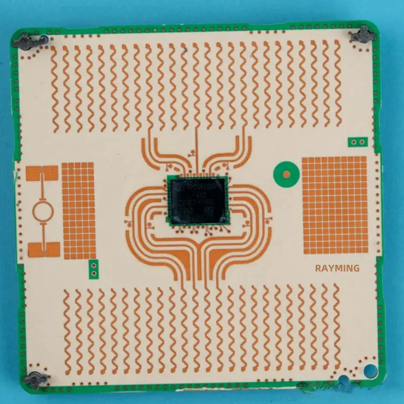
In today’s increasingly compact electronic devices, flexible and rigid-flex printed circuit boards (PCBs) have become essential components driving innovation across industries. From foldable smartphones to medical implants and aerospace applications, these versatile circuit boards enable designs that traditional rigid PCBs simply cannot achieve. At the heart of reliable flex and rigid-flex PCB design lies the IPC 2223 standard – a comprehensive set of guidelines ensuring consistency, reliability, and manufacturability.
What is IPC 2223?
IPC 2223 is the dedicated industry standard that provides detailed design guidelines specifically for flexible and rigid-flex printed circuit boards. As part of the broader IPC-2220 series (which covers design standards for all PCB types), IPC 2223 addresses the unique challenges and requirements associated with flex and rigid-flex technologies.
Unlike rigid PCBs, flexible circuits must maintain electrical integrity while being bent, folded, or dynamically flexed during operation. This fundamental difference introduces complexities that demand specialized design approaches. The IPC 2223 standard offers comprehensive guidance on materials, construction methods, dimensional requirements, and performance specifications that ensure flex and rigid-flex PCBs perform reliably throughout their intended lifecycle.
Design engineers who follow IPC 2223 benefit from decades of industry experience distilled into practical recommendations. The standard helps prevent common design pitfalls that often lead to premature circuit failure, such as improper bend radii, inadequate material selection, or inappropriate copper treatment in flex areas.
Powered By EmbedPress
Evolution of IPC 2223: Revisions and Versions
The IPC 2223 standard has evolved significantly since its initial release, reflecting technological advancements and addressing emerging challenges in flex and rigid-flex PCB design.
IPC 2223A
Released in the early 2000s, this version established the foundation for flex circuit design guidelines. It covered basic construction methods and material recommendations for single-sided, double-sided, and multilayer flex circuits.
IPC 2223B
This update expanded coverage of rigid-flex designs and introduced more detailed specifications for bend radii calculations. It also provided enhanced guidance on material selection considerations.
IPC 2223C
With this revision, the standard incorporated more comprehensive guidelines for controlled impedance in flex circuits – increasingly important as signal integrity requirements became more stringent in high-speed applications.
IPC 2223D
Released in 2016, IPC 2223D represented a significant overhaul. This version added substantial content addressing reliability enhancements, dynamic flex applications, and expanded design rules for emerging technologies like wearable electronics.
IPC 2223E
The latest revision as of 2025, IPC 2223E reflects cutting-edge developments in flex technology. This version includes enhanced guidelines for high-density interconnects (HDI) in flex applications, recommendations for flexible printed electronics, and updated material specifications reflecting new polyimide and adhesive technologies.
Staying current with the latest revision is crucial for several reasons. First, newer versions incorporate lessons learned from field failures and manufacturing challenges encountered after previous releases. Second, they address requirements for emerging applications and technologies not covered in earlier versions. Finally, the latest standards reflect current manufacturing capabilities and processes, ensuring designs are not only reliable but also producible at reasonable cost.
Among the most critical aspects of the IPC 2223 standard are the bend radius specifications. Improper bend design is a leading cause of flex circuit failure, making these guidelines particularly valuable.
Importance of Proper Bend Radius
The bend radius directly impacts the mechanical stress experienced by copper conductors during flexing. When the radius is too tight, copper traces experience excessive strain that can lead to cracking, especially during repeated flexing cycles. IPC 2223 provides detailed calculations to determine minimum safe bend radii based on circuit construction.
Standard Formulas and Recommendations
IPC 2223 offers specific formulas for calculating minimum bend radii. The basic calculation typically follows:
For single-flex applications (occasional bending during installation):
Minimum bend radius = 6 × total circuit thickness
For dynamic flex applications (repeated flexing during operation):
Minimum bend radius = 12 × total circuit thickness
Factors Affecting Bend Radius Requirements
The standard details how various design elements impact bend radius requirements:
Thickness of Flex Material
Thicker materials require larger bend radii to maintain the same strain levels. IPC 2223 provides specific multipliers based on material thickness.
Number of Layers
Multilayer flex circuits generally require larger bend radii than single or double-sided designs. The standard provides adjustment factors based on layer count.
Copper Type and Treatment
Rolled annealed copper generally tolerates tighter bend radii than electrodeposited copper due to its grain structure. IPC 2223 provides different recommendations based on copper type.
The standard also includes illustrated examples of proper bend designs, including:
Gradual bend implementations
Strain relief features
Recommended trace orientations relative to bend direction
Methods to distribute stress across larger areas
How to Access IPC 2223
As a critical industry standard, IPC 2223 is a valuable intellectual property developed through extensive expert collaboration and research.
Official Sources for IPC 2223
The only legitimate way to obtain the current IPC 2223 standard is through official channels:
Direct purchase from the IPC website (IPC.org)
Through authorized IPC document distributors
Via corporate IPC membership programs
Understanding PDF Download Limitations
It’s important to note that searching for “IPC 2223 PDF free download” or similar terms will likely lead to unauthorized copies or outdated versions. Using these carries several risks:
Potential copyright violations
Reliance on outdated or incomplete information
Missing critical updates that could affect product reliability
Cost-Effective Access Options
While the standard does require purchase, several legitimate cost-effective options exist:
IPC membership discounts (often 50% or more off standard prices)
Educational institution access programs
Standards subscription services for organizations needing multiple standards
The investment in obtaining the official standard is minimal compared to the potential cost of design failures resulting from following incorrect or outdated guidelines.
Practical Applications of IPC 2223
The IPC 2223 standard has enabled innovation across numerous industries by providing the foundation for reliable flex and rigid-flex implementations.
Medical Devices
The medical industry leverages IPC 2223 guidelines to create:
Implantable devices with biocompatible flex circuits
Wearable health monitors requiring comfortable, conformable electronics
Surgical tools incorporating flex circuits in space-constrained designs
Aerospace and Defense
This sector relies heavily on IPC 2223 for:
Satellite systems where weight reduction is critical
The IPC 2223 standard represents the collective wisdom of the flex and rigid-flex PCB industry, offering invaluable guidance for designers aiming to create reliable, manufacturable products. From precise bend radius calculations to material selection recommendations, this comprehensive standard addresses the unique challenges posed by flexible circuit technology.
Engineers working with flex and rigid-flex circuits should:
Always reference the latest IPC 2223 revision to benefit from the most current guidance
Pay particular attention to bend radius guidelines, as these directly impact long-term reliability
Consider the entire flex circuit ecosystem covered by the standard, from materials to manufacturing processes
By adhering to IPC 2223 guidelines, designers can avoid costly mistakes, accelerate development cycles, and produce flex and rigid-flex PCBs that deliver reliable performance throughout their intended lifecycle.
Frequently Asked Questions
What is the latest version of IPC 2223?
As of 2025, IPC 2223E is the most current revision of the standard. This version includes enhanced guidance for HDI in flex applications, flexible printed electronics, and updated material specifications reflecting new polyimide and adhesive technologies.
Where can I obtain an IPC 2223 PDF legally?
The only legitimate source for the IPC 2223 standard is through the official IPC website (IPC.org) or authorized distributors. While the standard must be purchased, IPC offers membership discounts that significantly reduce the cost.
How does IPC 2223 help reduce design failures?
IPC 2223 provides engineers with proven guidelines that address common failure modes in flex and rigid-flex circuits. By following the standard’s recommendations for bend radii, material selection, layer stackups, and other critical design elements, engineers can avoid mistakes that often lead to field failures and reliability issues.
Is IPC 2223 required for flex PCB manufacturing?
While not legally mandated, most reputable flex circuit manufacturers follow IPC 2223 guidelines as they represent industry-consensus best practices. Many customers specify compliance with IPC 2223 in their design requirements to ensure reliability and manufacturability.
How often is IPC 2223 updated?
The IPC typically reviews and updates standards like IPC 2223 every 5-7 years or when significant technological advancements warrant earlier revision. Design engineers should always verify they’re referencing the most current version available.
In the world of electronics and signal processing, few components are as fundamental and widely used as the low pass filter. These essential circuit elements play a crucial role in countless applications, from the audio systems in your home theater to life-saving medical devices. A low pass filter, as the name suggests, allows low-frequency signals to pass through while attenuating (reducing) signals with frequencies higher than a designated cutoff point. This seemingly simple function is the backbone of modern electronic systems, helping engineers and designers achieve cleaner signals, reduce noise, and extract only the information they need.
Whether you’re an electronics hobbyist, a student, or a seasoned engineer, understanding low pass filters is essential for designing effective electronic systems. This comprehensive guide explores everything you need to know about low pass filters in 2025, from basic principles to advanced design techniques, real-world applications, and emerging trends. We’ll break down the various types, explain how to design them for your specific needs, and provide practical tips to avoid common pitfalls.
A low pass filter (LPF) is an electronic circuit designed to allow signals below a specific cutoff frequency to pass through while attenuating (reducing) signals above that frequency. This fundamental function makes it one of the most important components in signal processing and electronic design.
Basic Principles of Operation
The operation of a low pass filter is based on the frequency-dependent behavior of capacitors and inductors. In simple terms, capacitors present high impedance (resistance) to low-frequency signals and low impedance to high-frequency signals. Inductors do the opposite, offering low impedance to lower frequencies and high impedance to higher frequencies. By strategically combining these components with resistors, engineers can create circuits that discriminate between signals based on their frequency content.
When a complex signal (containing multiple frequencies) enters a low pass filter, the circuit allows the low-frequency components to pass through relatively unchanged while progressively weakening higher-frequency components. The result is a “filtered” output signal that preserves the desired low-frequency information while reducing or eliminating unwanted high-frequency content.
Key Characteristics
Understanding the following key characteristics is essential for working with low pass filters:
Cutoff Frequency (fc): This defines the boundary between the passband and the stopband. It’s typically defined as the frequency at which the output power drops to half (-3dB) of the input power. The cutoff frequency is the primary specification when designing or selecting a low pass filter.
Roll-off Rate: This describes how quickly the filter attenuates frequencies above the cutoff point. It’s usually expressed in decibels per octave (dB/octave) or decibels per decade (dB/decade). A steeper roll-off means more effective filtering of unwanted frequencies.
Passband Ripple: Ideally, a filter would pass all frequencies below the cutoff with identical gain, but real filters often exhibit some variation (ripple) in the passband response.
Stopband Attenuation: This indicates how effectively the filter blocks frequencies in the stopband, typically measured in decibels.
Phase Response: Low pass filters don’t just affect signal amplitude—they also introduce phase shifts that vary with frequency. This can be critical in applications where timing relationships between signals must be preserved.
Filter Order: Higher-order filters (created by cascading multiple filter stages) provide steeper roll-off rates but introduce greater complexity, cost, and potential phase distortion.
Types of Low Pass Filters
Low pass filters come in various forms, each with distinct characteristics, advantages, and ideal use cases. Understanding these different types will help you select the right filter for your specific application.
1. Passive Low Pass Filter
Passive filters use only passive components—resistors, capacitors, and inductors—without any active elements like transistors or operational amplifiers. They’re the simplest form of filter and don’t require an external power supply.
In this circuit, the resistor and capacitor form a voltage divider whose division ratio varies with frequency. At low frequencies, the capacitor has high impedance, so most of the input voltage appears at the output. As frequency increases, the capacitor’s impedance decreases, causing more signal to be shunted to ground.
Advantages and Limitations
Advantages:
Simple and inexpensive
No power supply required
No active noise contribution
Can handle relatively high power levels
Reliable operation with minimal failure points
Limitations:
Fixed gain (typically less than unity)
Limited roll-off rate (usually 20 dB/decade per filter stage)
Potential loading effects on connected circuits
Less precise control over filter response
Cannot amplify signals
2. Active Low Pass Filter
Active filters incorporate active components, typically operational amplifiers (op-amps), alongside passive elements. These filters can provide gain, improved performance, and better isolation between stages.
Using Op-Amps and Other Active Components
Active low pass filters typically use op-amps as the active element, providing benefits like:
This circuit can provide gain determined by the ratio of R2 to R1 while maintaining the filtering action of the RC network.
Advantages and Limitations
Advantages:
Can provide signal gain
Minimal loading effect on connected circuits
Easily cascaded for higher-order filters
More control over filter response
Better performance at lower frequencies
Limitations:
Requires power supply
Bandwidth limitations of op-amps
Introduces noise and potential distortion
More complex design
Limited power handling capability
3. Digital Low Pass Filter
Digital filters implement filtering functions through software algorithms rather than physical components. They operate on discrete samples of signals in the digital domain.
Algorithmic Approach
Digital low pass filters process signals using mathematical operations like:
Requires analog-to-digital and digital-to-analog conversion
Processing delays
Limited by sampling rate and quantization effects
Higher power consumption for high-speed applications
Potential for aliasing issues
4. RC (Resistor-Capacitor) Low Pass Filter
RF Filter
The RC filter is the simplest form of low pass filter, consisting of just one resistor and one capacitor.
Basic RC Circuit Explanation
In an RC low pass filter, the resistor is placed in series with the signal path, and the capacitor is connected between the signal path and ground. The time constant (τ = RC) determines the filter’s behavior:
At low frequencies, the capacitor acts like an open circuit
At high frequencies, the capacitor acts like a short circuit
The cutoff frequency is given by: fc = 1/(2πRC)
Simple Design and Uses
An RC filter’s cutoff frequency is easily calculated using the formula above. For example:
A 10kΩ resistor and a 0.1µF capacitor yield a cutoff frequency of approximately 159Hz
A 1kΩ resistor and a 0.01µF capacitor result in a cutoff of about 15.9kHz
RC filters are commonly used in:
Audio tone controls
RF coupling circuits
Power supply smoothing
Anti-aliasing filters
Simple noise suppression
5. LC (Inductor-Capacitor) Low Pass Filter
LC filters use inductors and capacitors to form a resonant circuit that provides filtering action without the power losses associated with resistors.
Advantages in High-Frequency Applications
LC filters excel in high-frequency and high-power applications because:
RL filters use the frequency-dependent properties of inductors combined with resistors to create a low pass filter.
Basic Operation
In an RL low pass filter:
The inductor is placed in series with the signal path
The resistor is typically the load resistance or a parallel resistor
Low frequencies encounter minimal opposition from the inductor
High frequencies face increasing opposition from the inductor
Applications in Power Systems
RL filters are particularly useful in:
Motor control circuits
Power line conditioning
Inductive load driving
DC power supplies
Current smoothing applications
Applications of Low Pass Filters
RF Filters
Low pass filters are ubiquitous in electronic systems, playing crucial roles across numerous fields and applications. Understanding these applications provides insight into the versatility and importance of these fundamental components.
Audio Processing
In audio systems, low pass filters serve multiple essential functions:
Speaker Crossover Networks: Low pass filters direct only the low-frequency components to subwoofers and bass speakers, ensuring each speaker reproduces only the frequencies it’s designed to handle efficiently. This improves sound quality and protects speakers from damage.
Audio Equalization: Low pass filters form the foundation of equalizers, allowing sound engineers and audiophiles to shape frequency response for optimal sound reproduction or creative effects.
Subwoofer Integration: Dedicated low pass filters ensure that subwoofers receive only low-frequency content, typically below 80-120Hz, optimizing bass reproduction in home theater and professional audio systems.
Noise Reduction: By filtering out high-frequency noise while preserving the audio spectrum, low pass filters can improve signal-to-noise ratio in recording and playback systems.
Radio Communications
Communication systems rely heavily on low pass filtering:
Channel Filtering: Low pass filters isolate specific frequency bands, helping receivers extract desired signals from crowded radio spectrums.
Bandwidth Limitation: Regulatory requirements often specify maximum bandwidths for transmissions; low pass filters ensure compliance by restricting the spectrum of transmitted signals.
Intermediate Frequency (IF) Processing: In superheterodyne receivers, low pass filters help process intermediate frequency signals before final demodulation.
Signal Demodulation: Many demodulation schemes require low pass filtering to extract the original information signal from the carrier wave.
Power Supplies and Noise Reduction
Power supply design frequently incorporates low pass filters:
Ripple Reduction: Low pass filters smooth the rectified AC in power supplies, reducing ripple voltage and providing cleaner DC output.
EMI/RFI Suppression: Filters prevent high-frequency noise from entering sensitive circuits or radiating from power lines, helping devices meet electromagnetic compatibility (EMC) requirements.
Power Line Conditioning: Low pass filters block high-frequency noise on power lines, protecting sensitive equipment and improving performance.
Transient Suppression: By attenuating high-frequency components, properly designed filters can help mitigate the effects of voltage spikes and transients.
Digital Signal Smoothing
In digital systems, low pass filtering plays a key role:
Anti-Aliasing: Before analog-to-digital conversion, low pass filters restrict the signal bandwidth to prevent aliasing artifacts.
Data Smoothing: Digital low pass filters can reduce noise and extract trends from noisy data streams, valuable in applications from weather prediction to stock market analysis.
Sensor Signal Conditioning: Low pass filters remove high-frequency noise from sensor outputs, producing cleaner signals for processing.
Image Processing: In digital image manipulation, low pass filtering produces blurring effects and removes high-frequency noise, useful for preprocessing in computer vision applications.
Biomedical Engineering
Medical devices rely extensively on low pass filtering:
ECG Signal Processing: Low pass filters remove high-frequency interference while preserving the critical cardiac waveform information.
EEG Monitoring: Brain activity monitoring systems use low pass filters to isolate specific frequency bands of interest.
Medical Imaging: MRI, ultrasound, and other imaging technologies employ sophisticated filtering to enhance image quality and diagnostic value.
Patient Monitoring: Vital signs monitors use low pass filters to stabilize readings and reduce false alarms from transient noise.
Everyday Examples
Low pass filters are present in many everyday consumer devices:
Smartphone Touchscreens: Low pass filtering algorithms help distinguish intentional touches from inadvertent contact or electrical noise.
Camera Stabilization: Digital cameras use low pass filtering to smooth out handheld camera movements.
Home Wi-Fi Routers: RF sections employ low pass filters to ensure transmissions remain within allocated frequency bands.
Automotive Electronics: From engine control modules to infotainment systems, vehicles use numerous low pass filters for signal conditioning and noise reduction.
Creating an effective low pass filter requires careful planning and consideration of multiple factors. This step-by-step guide will help you design filters that meet your specific requirements.
1. Define Requirements
Before selecting components or drawing schematics, clearly establish what you need from your filter:
Cutoff Frequency
Determine the precise frequency boundary between signals you want to keep and those you want to attenuate. Consider:
The highest frequency component in your desired signal
The lowest frequency component you need to reject
Any transition band requirements
Desired Roll-off Rate
Decide how rapidly the filter should attenuate signals above the cutoff frequency:
Gentle roll-off (20 dB/decade): First-order filter, simpler but less effective
Moderate roll-off (40 dB/decade): Second-order filter, good compromise
Steep roll-off (60+ dB/decade): Higher-order filters, more complex but more effective
Passband and Stopband Specifications
Define the acceptable variation in your filter’s response:
Passband ripple: Maximum allowable amplitude variation for frequencies you want to pass
Stopband attenuation: Minimum required attenuation for frequencies you want to reject
Transition band width: How quickly the filter transitions from pass to reject
2. Choose Filter Type
Based on your requirements, select the most appropriate filter category:
Analog vs. Digital
Consider:
Operating environment (analog or digital domain)
Available processing resources
Required precision and flexibility
Budget constraints
Active vs. Passive
Consider:
Power availability
Required gain
Circuit complexity
Noise sensitivity
Available space
Filter Response Type
Different mathematical models offer different performance characteristics:
Machine learning algorithms predict and compensate for component aging
Self-tuning filters adjust their characteristics based on real-time signal analysis
AI-optimized filter architectures outperform traditionally designed filters
Reduced computational requirements through intelligent algorithm selection
These smart filters are particularly valuable in applications with varying signal characteristics or challenging noise environments.
Integrated Solutions in ICs
Modern integrated circuit technology incorporates increasingly sophisticated filtering capabilities:
Complete filter solutions in single-chip packages
Programmable analog filters with digital control
Switched-capacitor implementations with exceptional precision
Software-defined filtering architectures
Mixed-signal approaches combining the best of analog and digital techniques
These integrated solutions reduce component count, improve reliability, and lower system cost while offering performance that was previously unattainable.
Advanced Materials and Techniques
Novel materials and fabrication methods are expanding filter capabilities:
High-Q ceramic resonators for RF applications
Superconducting filters for quantum computing systems
Metamaterial structures creating previously impossible frequency responses
Carbon nanotube-based components with exceptional performance
3D-printed RF structures for custom filter responses
These advances particularly benefit specialized applications with extreme requirements for selectivity, power handling, or size constraints.
Conclusion
Low pass filters represent one of the fundamental building blocks of electronic systems, performing the crucial task of separating wanted signals from unwanted ones based on frequency content. From the simplest RC network to sophisticated digital implementations, these filters enable countless technologies that we rely on daily. As we’ve explored in this guide, low pass filters come in many forms, each with distinct advantages and ideal applications.
When designing or selecting a low pass filter, remember to clearly define your requirements first, then choose the appropriate filter type and topology that best matches those needs. Pay close attention to component selection, and always verify your design through simulation and testing before final implementation. By avoiding common pitfalls and staying aware of the latest developments in filter technology, you can create efficient, effective filtering solutions for even the most demanding applications.
As technology continues to advance, we can expect even more innovative approaches to filtering, with improvements in size, performance, and integration. However, the fundamental principles of low pass filtering will remain essential knowledge for anyone working with electronic systems and signal processing.
FAQs About Low Pass Filters
What is the best low pass filter for audio applications?
The “best” filter depends on your specific requirements, but Butterworth filters are often preferred for audio because they provide maximally flat frequency response in the passband, avoiding coloration of the audio. For crossovers, Linkwitz-Riley filters (which are cascaded Butterworth filters) are popular because they provide -6dB response at the crossover point when summed with their high-pass counterparts. For applications where phase response is critical, Bessel filters may be preferred due to their linear phase characteristics, which preserve the waveform shape.
Can I use a low pass filter for DC signals?
Yes, low pass filters work perfectly with DC signals since DC is essentially a signal with zero frequency, which falls well within the passband of any low pass filter. In fact, one common application of low pass filters is extracting the DC component from a mixed signal. However, if your signal is purely DC with no AC components, a filter wouldn’t be necessary unless you’re trying to remove noise or ripple.
How do I calculate the cutoff frequency?
The formula depends on the filter type:
For RC filters: fc = 1/(2πRC)
For RL filters: fc = R/(2πL)
For LC filters: fc = 1/(2π√(LC))
For active filters: depends on the specific topology, but many follow the RC formula
Where:
fc is the cutoff frequency in Hz
R is resistance in ohms
C is capacitance in farads
L is inductance in henries
Online calculators and design tools can simplify these calculations for more complex filter types.
Passive vs. active low pass filter: which is better?
Neither is inherently “better” as each has advantages for different situations:
Choose passive filters when:
No power source is available
Simplicity is paramount
Working with high power levels
High reliability is essential
Working at very high frequencies
Choose active filters when:
Signal amplification is needed
Precise filter characteristics are required
Multiple filter stages must be cascaded
Input/output impedance matching is important
Working with very low frequencies
For many modern applications, active filters are preferred due to their flexibility and performance, but passive filters remain important in power electronics, RF design, and other specialized fields.
How do I design a low pass filter for a specific application?
Start by defining your requirements precisely:
Determine the required cutoff frequency
Identify necessary attenuation rate (roll-off)
Consider any phase response requirements
Define acceptable passband ripple
Consider physical constraints (size, cost, power)
Then: 6. Select an appropriate filter topology 7. Calculate component values using formulas or design tools 8. Choose actual components considering tolerances and non-idealities 9. Simulate your design with realistic component models 10. Build and test a prototype before final implementation
For complex filters, specialized design software can greatly simplify this process.
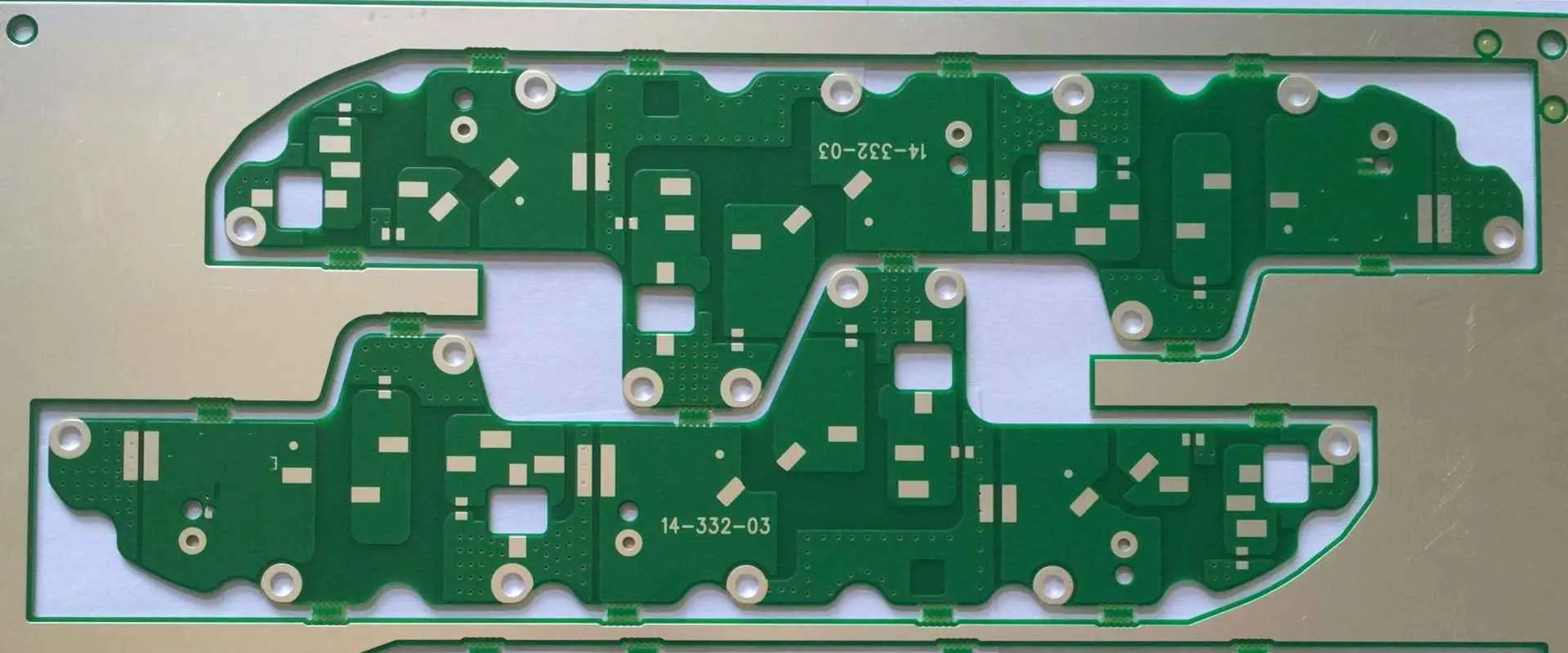
High-frequency circuit boards are essential components in modern electronic systems, particularly in telecommunications, aerospace, and defense applications. Rogers Corporation is a leading manufacturer of high-performance circuit materials specifically designed for these demanding applications. When current flows through these circuit boards—whether direct current (DC) or radio frequency (RF) current—heat is generated due to various loss mechanisms. Understanding and accurately estimating the resulting temperature rise is crucial for ensuring reliable operation and preventing premature failure of electronic systems.
Powered By EmbedPress
Theoretical Background of Heat Generation
The temperature rise in circuit boards is primarily caused by resistive losses (I²R losses) when current flows through conductive traces. For DC currents, the heat generation is relatively straightforward, governed by Joule’s heating law. However, for RF currents, additional loss mechanisms come into play, making temperature estimation more complex.
When RF current flows through a circuit board, losses occur due to:
Conductor losses – Resistive losses in the copper traces
Dielectric losses – Energy dissipated within the substrate material
Radiation losses – Energy converted to electromagnetic radiation
Rogers high-frequency materials are specifically engineered to minimize these losses, particularly at microwave and millimeter-wave frequencies. Materials such as RO4000® series, RT/duroid®, and CLTE™ offer low dielectric losses (characterized by low dissipation factor or tanδ) and stable electrical properties across frequency and temperature ranges.
For direct current applications, the temperature rise can be estimated using thermal resistance models. The key equation is:
ΔT = P × Rth
Where:
ΔT is the temperature rise above ambient (°C)
P is the power dissipated (watts)
Rth is the thermal resistance (°C/W)
The power dissipated is calculated using P = I²R, where I is the current and R is the resistance of the trace. The resistance depends on the trace dimensions (width, thickness) and the resistivity of copper, which may vary slightly with temperature.
The thermal resistance depends on multiple factors:
Rogers materials typically have thermal conductivities ranging from 0.2 to 0.7 W/m·K, which is relatively low compared to ceramic substrates but higher than many conventional FR-4 materials.
RF Current Temperature Rise Estimation
For RF currents, the situation becomes more complex due to frequency-dependent effects. The estimation process requires consideration of:
Skin effect – At high frequencies, current flows primarily near the surface of conductors, effectively increasing resistance
Dielectric loss factor – Energy dissipated in the substrate material
Impedance matching – Mismatches can create standing waves, concentrating power at specific locations
The power dissipation for RF signals can be calculated using:
P = Pin × (1-|S21|²-|S11|²)
Where:
Pin is the input power
S21 is the transmission coefficient (power delivered to load)
S11 is the reflection coefficient (power reflected back to source)
This calculation accounts for both the power transmitted through the circuit and the power reflected due to impedance mismatches.
While theoretical calculations provide a foundation, empirical methods often yield more accurate temperature rise estimations for specific board configurations:
Reference designs – Using documented temperature rises from similar designs
Thermal modeling software – Finite element analysis (FEA) tools that account for material properties and boundary conditions
Infrared thermal imaging – Direct measurement of operating temperatures under various load conditions
Rogers Corporation provides thermal data sheets and application notes for their materials, which can serve as valuable references for temperature rise estimation.
Critical Factors Affecting Temperature Rise
Several key factors significantly impact temperature rise in Rogers high-frequency circuit boards:
Substrate Material Properties
Different Rogers materials exhibit varying thermal characteristics:
RT/duroid® 5880 has a thermal conductivity of approximately 0.20 W/m·K
RO4350B™ offers improved thermal conductivity around 0.62 W/m·K
TC350™ is specifically designed for thermal management with conductivity up to 1.0 W/m·K
Copper Thickness and Trace Width
Wider traces and thicker copper layers provide lower resistance paths for current flow, reducing power dissipation. Standard copper thicknesses range from 1/2 oz (17.5 μm) to 2 oz (70 μm) for Rogers materials, with custom thicknesses available for high-current applications.
Thermal Management Techniques
Several techniques can be employed to mitigate temperature rise:
Thermal vias – Connecting to internal ground planes or heat sinks
Copper pours – Increasing the effective copper area for heat spreading
Thermally conductive adhesives – Improving heat transfer to enclosures or heat sinks
Forced air cooling – Enhancing convection cooling around the board
Practical Estimation Approach
A systematic approach to estimating temperature rise includes:
Calculate the DC resistance of the trace using dimensions and material properties
For RF applications, calculate the effective resistance accounting for skin effect
Determine power dissipation using appropriate equations for DC or RF current
Estimate thermal resistance based on board construction and cooling methods
Calculate temperature rise using ΔT = P × Rth
Apply safety factors to account for uncertainties
Case Studies
Example 1: DC Power Distribution Trace
Consider a 50 mil (1.27 mm) wide, 1 oz copper trace on RO4350B carrying 2 amperes of DC current. The trace resistance is approximately 0.02 ohms per inch. For a 3-inch trace:
Total resistance = 0.06 ohms
Power dissipation = (2 A)² × 0.06 Ω = 0.24 watts
With a thermal resistance of approximately 30°C/W for this configuration
Temperature rise = 0.24 W × 30°C/W = 7.2°C above ambient
Example 2: RF Power Amplifier Output Line
For a 50-ohm microstrip line on RT/duroid 6010 carrying 5 watts of RF power at 10 GHz:
Insertion loss ≈ 0.2 dB/inch (primarily from conductor and dielectric losses)
For a 2-inch line, total loss ≈ 0.4 dB or approximately 9% of power
Power dissipation = 5 W × 0.09 = 0.45 watts
With a thermal resistance of approximately 25°C/W for this configuration
Temperature rise = 0.45 W × 25°C/W = 11.25°C above ambient
Verification Methods
Temperature rise estimations should always be verified using:
Thermal imaging cameras to identify hot spots
Thermocouples or RTDs placed at critical locations
Temperature-sensitive paint or labels for visual indication
Load testing under worst-case operating conditions
Conclusion
Accurate estimation of temperature rise in Rogers high-frequency circuit boards requires understanding both the electrical and thermal properties of the materials involved. While DC current temperature rise calculations are relatively straightforward, RF applications demand consideration of additional frequency-dependent effects. By using a combination of theoretical calculations, empirical data, and verification measurements, engineers can ensure that their high-frequency designs maintain acceptable operating temperatures.
As operating frequencies continue to increase and electronic packaging becomes more compact, thermal management will remain a critical aspect of high-frequency circuit design. Rogers Corporation continues to develop materials with improved thermal properties while maintaining excellent electrical characteristics, enabling the next generation of high-performance RF and microwave systems.
In today’s rapidly evolving automotive industry, radar technology has become a cornerstone of vehicle safety and autonomous driving capabilities. Among the most significant technological shifts in recent years is the transition from 24GHz to 77GHz radar systems. This change represents more than just a numerical upgrade – it marks a fundamental improvement in how vehicles perceive and interact with their surroundings. As automotive manufacturers and suppliers race to develop safer, more intelligent vehicles, understanding the advantages and implications of 77GHz radar technology has become essential knowledge for industry professionals and tech enthusiasts alike.
Understanding Automotive Radar Frequencies
Before diving into the specific benefits of 77GHz radar, it’s important to understand the fundamental differences between the two major frequency bands used in automotive applications.
What is 24GHz Radar?
24GHz radar systems have been the workhorses of automotive sensing for over two decades. Operating in the K-band of the electromagnetic spectrum (24.05-24.25 GHz), these systems were revolutionary when first introduced, enabling features like basic blind-spot detection and simple adaptive cruise control. Their relatively low cost and established manufacturing processes made them the default choice for early Advanced Driver Assistance Systems (ADAS).
The 24GHz radar technology operates in two primary bands:
Narrow-band (24.05-24.25 GHz)
Ultra-wideband (21.65-26.65 GHz)
While these systems provided adequate performance for basic safety features, their limitations in range, resolution, and interference management became increasingly apparent as automotive safety demands evolved.
What is 77GHz Radar?
77GHz radar represents the next generation of automotive sensing, operating in the W-band (76-81 GHz) of the electromagnetic spectrum. This significantly higher frequency enables dramatic improvements in performance across multiple dimensions. The 77GHz radar leverages millimeter-wave technology to achieve sensing capabilities that simply weren’t possible with previous generations.
The 77GHz band typically spans from 76 to 81 GHz, providing a much wider bandwidth than 24GHz systems. This expanded bandwidth is crucial for next-generation automotive applications, particularly those requiring high-resolution imaging and precise object detection.
Why Frequency Matters for Radar Systems
The fundamental physics behind radar operation explains why the shift to higher frequencies delivers such substantial benefits. Radar works by transmitting radio waves that bounce off objects and return to the sensor. The properties of these waves—including wavelength, beam width, and propagation characteristics—are directly influenced by their frequency.
Higher frequency waves (like 77GHz) have shorter wavelengths, which enable:
More precise measurement of object position and velocity
Better discrimination between closely spaced objects
Smaller antenna size for a given level of performance
Improved resistance to certain types of interference
These physical advantages translate directly into real-world performance improvements that are driving the industry-wide shift toward 77GHz technology.
The transition from 24GHz to 77GHz radar brings several critical advantages that directly impact vehicle safety and autonomous driving capabilities.
Higher Resolution and Accuracy
The most immediately noticeable benefit of 77GHz radar is its dramatically improved resolution. Resolution in radar terms refers to the ability to distinguish between objects that are close together.
Improved Object Detection
77GHz radar can detect smaller objects at greater distances than 24GHz systems. This improvement is particularly important for identifying vulnerable road users like pedestrians and cyclists, as well as potentially hazardous debris on the roadway.
The angular resolution of 77GHz radar is typically 1-2 degrees, compared to 5-10 degrees for 24GHz systems. This finer angular resolution means that vehicles can more precisely locate objects in their environment, leading to more accurate decision-making by ADAS systems.
Narrower Beam Width
The higher frequency of 77GHz radar naturally produces a narrower beam width. This focused energy allows the radar to:
Provide more precise angular measurements
Reduce false detections from adjacent lanes
Better identify the edges and boundaries of objects
Maintain performance even in complex driving environments
These capabilities are essential for advanced features like automatic emergency braking and lane-keeping assistance, where precise object location is critical for safe operation.
Greater Detection Range
One of the most significant advantages of 77GHz radar is its extended detection range.
Longer Sensing Distance
77GHz radar systems typically achieve effective ranges of 200-300 meters, compared to the 70-100 meter range of traditional 24GHz systems. This extended range provides crucial additional seconds of reaction time at highway speeds, allowing vehicles to:
Begin braking earlier for obstacles
Make more gradual speed adjustments
Plan lane changes and maneuvers with greater foresight
Maintain safer following distances in adaptive cruise control
Real-World Applications
This extended range is particularly valuable for highway driving scenarios, where vehicle speeds are high and early detection of traffic patterns is essential. Practical applications include:
Long-range adaptive cruise control that can track vehicles at distances of 200+ meters
Early collision warning systems that provide more time for driver response
Highway autopilot features that can anticipate traffic flow changes well in advance
Improved all-weather performance, maintaining reliable detection even in fog, rain, and snow
Smaller Antenna Size
The physics of radar mean that higher frequency systems can achieve comparable performance with significantly smaller antenna sizes.
Compact Design Advantages
77GHz radar modules are typically 50-70% smaller than equivalent 24GHz units. This size reduction offers multiple benefits:
More flexible mounting options around the vehicle
Less intrusive integration into vehicle styling
Ability to place multiple radar units for 360-degree coverage
Reduced impact on vehicle aerodynamics and design aesthetics
Multi-Radar Integration
The compact size of 77GHz radar units makes it practical to integrate multiple sensors around the vehicle, creating a comprehensive sensing network. Modern vehicles often incorporate 4-6 radar sensors, providing overlap between detection zones and redundancy for safety-critical functions.
Regulatory Changes Driving the Shift
Beyond the technical advantages, regulatory factors are accelerating the transition to 77GHz radar technology.
Global Regulatory Landscape
Telecommunications regulatory bodies worldwide have been coordinating a managed transition from 24GHz to 77GHz radar for automotive applications:
The Federal Communications Commission (FCC) in the United States has allocated the 76-81 GHz band specifically for vehicular radar systems.
The European Telecommunications Standards Institute (ETSI) has similarly designated the 77GHz band for automotive use while phasing out certain 24GHz applications.
Similar regulatory frameworks have been adopted in Japan, China, South Korea, and other major automotive markets.
Phase-Out of 24GHz Ultra-Wideband
Perhaps the most significant regulatory driver is the planned phase-out of ultra-wideband 24GHz radar systems. These systems were always approved on a temporary basis, as they operated in frequency bands shared with other critical applications, including:
Earth exploration satellite services
Radio astronomy
Fixed wireless communications
To address potential interference concerns, regulatory bodies have established timelines for the transition away from these temporary allocations, pushing manufacturers toward 77GHz technology.
Environmental and Spectrum Management Considerations
The shift to 77GHz also reflects broader goals in efficient spectrum management. The 77GHz band provides dedicated spectrum for automotive applications, reducing potential conflicts with other services and allowing for more effective management of this limited resource.
However, these costs are decreasing as production volumes increase and manufacturing processes mature.
Calibration and Testing Requirements
Higher frequency radar systems require more precise calibration to maintain their performance advantages:
More sophisticated alignment procedures during manufacturing
Field calibration requirements after vehicle repairs
Specialized testing equipment for validation
Integration with Sensor Fusion Systems
Modern vehicles rely on multiple sensing technologies working together, including cameras, lidar, and ultrasonic sensors. Integrating 77GHz radar into these comprehensive sensing systems requires careful engineering to:
Harmonize detection ranges and fields of view
Reconcile different data formats and update rates
Manage sensor redundancy and fault tolerance
Optimize overall system performance
The Future of Automotive Sensing: Beyond 77GHz?
While 77GHz radar represents the current state-of-the-art, the technology continues to evolve.
Emerging 79GHz Ultra-Wideband Radar
Even higher frequency systems operating in the 79GHz band (77-81 GHz) are beginning to emerge. These systems offer:
Even finer resolution for detailed environmental mapping
Potential for radar-based imaging applications
Better discrimination of complex objects
Sensor Fusion and AI Integration
The future of automotive sensing lies not just in better individual sensors, but in smarter integration:
Deep learning algorithms that enhance radar signal processing
Fusion of radar, lidar, and camera data for comprehensive perception
Real-time environmental mapping and prediction
Beyond Traditional Automotive Applications
The capabilities of advanced radar systems are enabling applications beyond basic safety:
Vehicle-to-everything (V2X) communication augmentation
Infrastructure monitoring and smart city integration
Advanced weather sensing and road condition detection
Conclusion
The transition from 24GHz to 77GHz radar represents one of the most significant technological shifts in automotive safety systems. The superior performance characteristics of 77GHz radar—including extended range, higher resolution, and compact form factor—provide the sensing capabilities required for advanced driver assistance and autonomous driving features.
As regulatory changes continue to phase out older 24GHz technologies, vehicle manufacturers and suppliers are investing heavily in 77GHz radar systems. This shift is not merely a response to regulations but a recognition of the fundamental advantages that 77GHz technology brings to vehicle safety and capability.
For automotive engineers, system integrators, and technology strategists, embracing 77GHz radar technology is not just about compliance—it’s about enabling the next generation of intelligent vehicles that can perceive their environment with unprecedented clarity and precision. As the industry continues its march toward autonomous driving, 77GHz radar will remain a cornerstone technology, providing the reliable, high-performance sensing that makes these advanced systems possible.
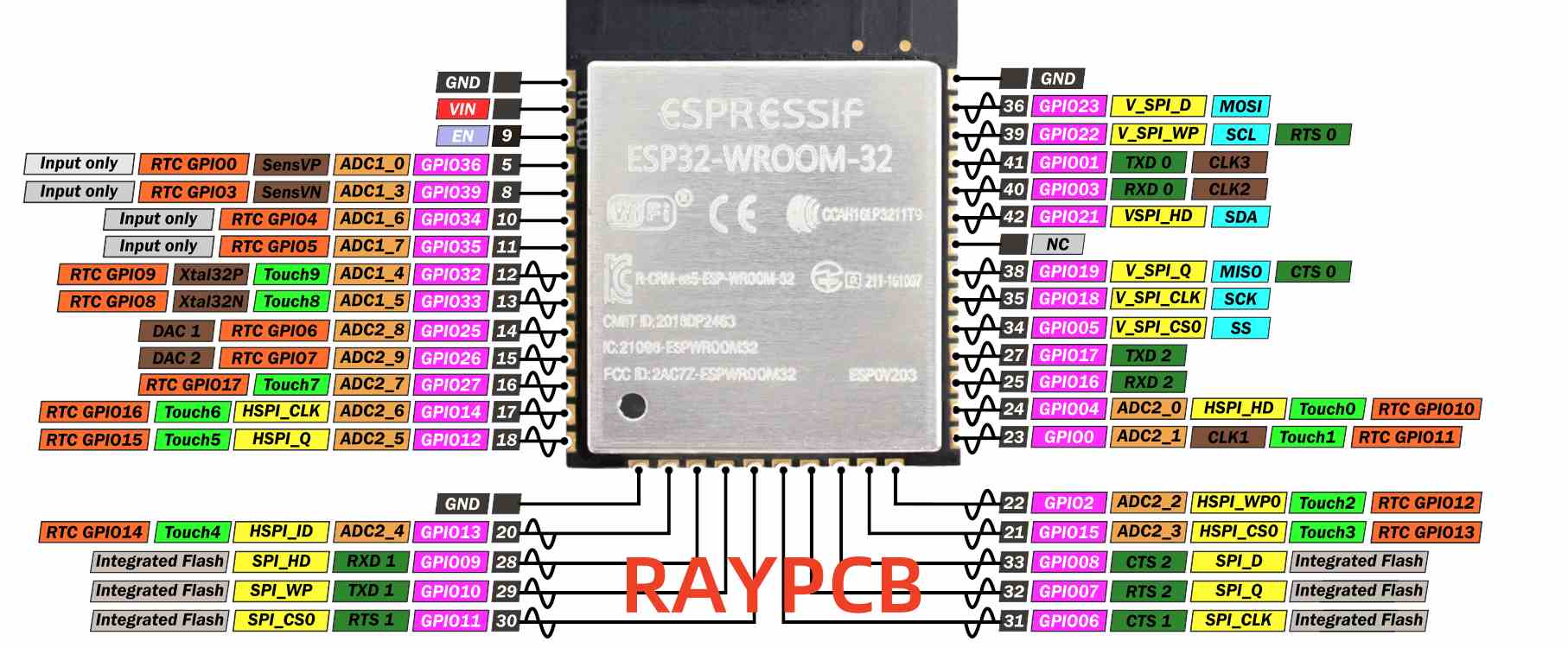
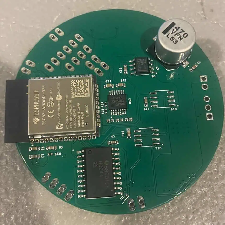
Are you looking to get started with ESP32 development using the Arduino IDE? Whether you’re working with the popular ESP32 WROOM32 or the newer ESP32-C3 boards, this comprehensive guide will walk you through the entire setup process. From installing the necessary software to troubleshooting common issues, you’ll learn everything needed to successfully flash code to your ESP32 devices.
Why Choose ESP32 for Your Projects?
The ESP32 microcontroller family has revolutionized IoT development with its powerful features and affordable price point. Before diving into the setup process, let’s understand what makes ESP32 boards so popular among hobbyists and professionals alike.
Features and Capabilities of ESP32 Boards
ESP32 boards pack impressive capabilities into a small form factor. They support both Wi-Fi and Bluetooth connectivity, feature dual-core processors (in the WROOM32 variant), and offer numerous GPIO pins for connecting external components. The ESP32-C3 variant brings RISC-V architecture to the table, offering excellent performance while maintaining compatibility with existing ESP32 code.
These versatile microcontrollers can operate on low power, making them ideal for battery-operated devices and IoT applications. With built-in touch sensors, temperature sensors, and hall effect sensors, ESP32 boards provide a complete solution for a wide range of projects.
Comparing WROOM32 and C3 Variants
When selecting an ESP32 board for your project, understanding the differences between variants is crucial:
ESP32 WROOM32: Features a dual-core processor, more GPIO pins, and generally higher processing power. Ideal for complex projects requiring substantial computational resources.
ESP32-C3: Utilizes a single-core RISC-V processor, offers smaller form factor, lower power consumption, and reduced cost. Perfect for simpler IoT applications where size and power efficiency are priorities.
Both variants support Arduino IDE programming, making them accessible to developers familiar with the Arduino ecosystem.
Let’s start with the essential steps to configure your Arduino IDE for ESP32 programming.
Installing Arduino IDE
Before programming ESP32 boards, you’ll need the Arduino IDE installed on your computer. If you’re just starting with ESP32, Arduino IDE is recommended for its simplicity and intuitive interface.
The process to install Arduino IDE is straightforward:
Select the appropriate installer for your operating system (Windows, macOS, or Linux)
Follow the installation prompts to complete the setup
You can choose between Arduino IDE 1.x and the newer Arduino IDE 2.x versions. Both support ESP32 development, but the setup process differs slightly between them.
Adding ESP32 Board Support to Arduino IDE 1.x
To program the ESP32 using Arduino IDE, you’ll need to install an add-on that enables the ESP32 board compatibility with Arduino’s programming language. Follow these steps to add ESP32 support:
Open Arduino IDE
Navigate to File > Preferences
In the “Additional Board Manager URLs” field, add: https://raw.githubusercontent.com/espressif/arduino-esp32/gh-pages/package_esp32_index.json
Click “OK” to save the preferences
Go to Tools > Board > Boards Manager
Search for “ESP32”
Find “ESP32 by Espressif Systems” and click “Install”
Wait for the installation to complete and restart Arduino IDE
Adding ESP32 Board Support to Arduino IDE 2.x
For the newer Arduino IDE 2.x, the process to add ESP32 support is slightly different but equally straightforward. Here’s how:
Open Arduino IDE 2.x
Click the Boards Manager icon in the left sidebar (or go to Tools > Board > Boards Manager)
Search for “ESP32”
Find “ESP32 by Espressif Systems” and click “Install”
Select version 2.0.11 or newer from the dropdown menu
Wait for the installation to complete
Configuring Your ESP32 Board
After installing the ESP32 board support, you need to configure Arduino IDE for your specific board model.
Setting Up WROOM32 Boards
To configure Arduino IDE for ESP32 WROOM32 boards:
Connect your ESP32 WROOM32 board to your computer via USB
In Arduino IDE, go to Tools > Board > ESP32 Arduino
Select “ESP32 Dev Module” or “DOIT ESP32 DEVKIT V1” (depending on your board model)
Set the following parameters under the Tools menu:
Under Tools > Port, select the COM port where your ESP32 is connected
If you don’t see any available ports, you may need to install the appropriate USB drivers for your board.
Setting Up ESP32-C3 Boards
For ESP32-C3 boards, the configuration is slightly different. After connecting your board to the computer, select the corresponding board model and port. Follow these steps:
Connect your ESP32-C3 board to your computer via USB
In Arduino IDE, go to Tools > Board > ESP32 Arduino
Select “ESP32C3 Dev Module” or your specific C3 board model
Configure the following settings:
Upload Speed: 460800
USB CDC On Boot: Enabled (important for ESP32-C3)
CPU Frequency: 160MHz
Flash Frequency: 80MHz
Flash Mode: QIO
Flash Size: 4MB
Partition Scheme: Default 4MB with spiffs
Core Debug Level: None
Select the appropriate port under Tools > Port
Installing USB Drivers
Many ESP32 boards require specific USB drivers to be recognized by your computer.
Common Driver Types
ESP32 development boards typically use USB-to-serial converter chips that may require driver installation before you can upload code to your board. The most common types are:
CP210x: Used in many ESP32 DevKit boards and the WROOM32 module
CH340/CH341: Found in lower-cost ESP32 boards and many ESP32-C3 variants
Installing Drivers on Different Operating Systems
Driver installation varies by operating system:
Windows:
Download the appropriate driver from the manufacturer’s website
Run the installer and follow the prompts
You may need to restart your computer after installation
macOS:
Download the macOS version of the driver
Open the installer package and follow the instructions
You may need to authorize the driver in System Preferences > Security & Privacy
Linux:
Most Linux distributions include the necessary drivers by default
For some boards, you may need to add your user to the “dialout” group with the command: sudo usermod -a -G dialout $USER
Log out and log back in for the changes to take effect
Uploading Your First Sketch
Now let’s test your setup by uploading a simple sketch to your ESP32.
Basic Blink Sketch
To test the ESP32 board installation, upload a simple code that blinks the on-board LED (typically connected to GPIO 2). Here’s a basic sketch to try:
cpp// Simple blink sketch for ESP32// LED pin varies by board - GPIO 2 is common for WROOM32, GPIO 8 for many C3 boards
#define LED_PIN 2 // Change to 8 for ESP32-C3 if needed
void setup() {
pinMode(LED_PIN, OUTPUT);
Serial.begin(115200);
Serial.println("ESP32 Blink Test");
}
void loop() {
digitalWrite(LED_PIN, HIGH);
Serial.println("LED ON");
delay(1000);
digitalWrite(LED_PIN, LOW);
Serial.println("LED OFF");
delay(1000);
}
Putting ESP32 in Boot Mode
Some ESP32 boards don’t automatically enter programming mode when uploading code. If you encounter issues, you may need to manually enter boot mode by pressing specific button combinations.
For WROOM32 boards:
Press and hold the BOOT button
Click the upload button in Arduino IDE
When you see “Connecting…” in the console, release the BOOT button
For ESP32-C3 boards:
Press and hold the BOOT button
Press the RESET button once while holding BOOT
Release the BOOT button
Click upload in Arduino IDE
Monitoring Serial Output
After uploading your sketch:
Open the Serial Monitor by clicking the icon in the top-right corner or navigating to Tools > Serial Monitor
Set the baud rate to 115200
You should see the “LED ON” and “LED OFF” messages alternating every second
The onboard LED should blink accordingly
Troubleshooting Common Issues
Even with careful setup, you might encounter some challenges. Here are solutions to the most common problems.
Connection and Upload Problems
If you’re having trouble uploading code to your ESP32:
Port not found:
Ensure your board is properly connected
Install or reinstall the appropriate USB drivers
Try a different USB cable (some cables are charge-only)
Upload timeout: If you see the error “A fatal error occurred: Failed to connect to ESP32: Timed out… Connecting…” it means your ESP32 is not in flashing/uploading mode.
Follow the boot mode instructions mentioned earlier
For persistent issues, try lowering the upload speed in Tools menu
Board not responding:
Press the reset button on your ESP32 board
Disconnect and reconnect the USB cable
Restart Arduino IDE
Serial Communication Issues
If you can upload code but don’t see serial output:
No data in Serial Monitor: Lowering the baud rate can help stabilize the serial communication, especially if you’re using a lower-quality USB cable or a system with limited resources.
Ensure your Serial Monitor baud rate matches the one in your code (typically 115200)
Check that your code includes Serial.begin(115200) in the setup function
Garbled characters:
Verify that the baud rate in Serial Monitor matches your code
Try a different USB cable or port
For ESP32-C3 boards, ensure “USB CDC On Boot” is enabled in the Tools menu
Advanced ESP32 Features with Arduino IDE
Once you’ve mastered the basics, you can explore more advanced capabilities of your ESP32 board.
Wi-Fi and Bluetooth Functionality
ESP32’s built-in wireless connectivity can be easily accessed through Arduino libraries:
For Wi-Fi, use the WiFi.hlibrary to connect to networks, create access points, or implement web servers
For Bluetooth, the BluetoothSerial.h library enables classic Bluetooth functionality, while BLEDevice.h provides Bluetooth Low Energy support
Working with ESP32 Peripherals
ESP32 boards offer numerous peripherals that can be controlled through Arduino code:
Analog-to-Digital Conversion: Use analogRead() to read values from the ADC pins
Digital-to-Analog Conversion: The dacWrite() function outputs analog voltages on supported pins
Touch Sensors: Access the capacitive touch sensors with touchRead() functions
PWM Control: Create precise PWM signals using the ledc functions for motor control or LED dimming
File System and Data Storage
ESP32 supports various file systems for data storage:
SPIFFS: A simple file system for the flash memory, accessible through the SPIFFS library
LittleFS: A more robust alternative to SPIFFS with better wear leveling
SD Card: Interface with SD cards using the SD library for expanded storage capacity
Project Examples for ESP32 WROOM32 and C3
Let’s explore some practical applications for your newly configured ESP32 boards.
IoT Weather Station
Create a simple weather station that monitors temperature, humidity, and pressure:
Send data to a cloud platform like ThingSpeak or create a local web server to display readings
Implement sleep modes to conserve battery life for remote installations
Smart Home Controller
Transform your ESP32 into a smart home hub:
Use relays to control household appliances
Implement a web interface or mobile app for remote control
Add sensors to create automation rules based on environmental conditions
Integrate with existing smart home platforms like Home Assistant or MQTT brokers
Differences in Implementation Between WROOM32 and C3
When developing projects for different ESP32 variants, keep these considerations in mind:
GPIO Assignments: Pin numbering and available pins differ between models
Power Consumption: C3 generally consumes less power, making it better for battery-operated devices
Processing Power: WROOM32’s dual-core architecture handles complex tasks more efficiently
Memory Constraints: Adjust your code complexity based on the available RAM and flash memory
Conclusion
Setting up the Arduino IDE for ESP32 development opens up a world of possibilities for your DIY electronics projects. Whether you’re working with the powerful ESP32 WROOM32 or the energy-efficient ESP32-C3, this guide has equipped you with the knowledge to install the necessary software, configure your boards, and start programming.
Remember that the ESP32 ecosystem is constantly evolving, with new board variants and software updates appearing regularly. Stay connected with the ESP32 community through forums and the official Espressif documentation to keep up with the latest developments.
With your ESP32 Arduino setup complete, you’re ready to explore the full potential of these versatile microcontrollers. From simple LED blink projects to sophisticated IoT applications, the ESP32 platform offers the perfect balance of performance, features, and affordability for makers at all skill levels.
The world of Internet of Things (IoT) and embedded systems is evolving rapidly, with new microcontrollers and System-on-Chip (SoC) solutions emerging to meet diverse project requirements. Among the popular choices for developers and engineers are the ESP32 series modules from Espressif Systems. Two notable contenders in this series are the ESP32-WROOM and the ESP32-C3. This comprehensive comparison will delve into the key differences between these modules, helping you make an informed decision for your next project.
In this article, we’ll explore the unique features, capabilities, and best use cases for both the ESP32-WROOM and ESP32-C3. By the end, you’ll have a clear understanding of which module is best suited for your specific needs, whether you’re working on a high-performance IoT application, a low-power device, or a cost-sensitive project.
The ESP32-WROOM is a powerful and versatile module that has become a staple in many IoT and embedded projects. It’s known for its robust performance, extensive feature set, and wide range of capabilities.
Complex IoT systems requiring significant processing power
ESP32-C3
General Description
The ESP32-C3 is a more recent addition to the ESP32 family, designed with a focus on cost-effectiveness, power efficiency, and enhanced security features. It aims to provide a balance between performance and energy consumption.
One of the most significant differences between the ESP32-WROOM and ESP32-C3 lies in their processor architecture.
ESP32-WROOM: Dual-core Tensilica Xtensa
The ESP32-WROOM features a dual-core Tensilica Xtensa LX6 microprocessor. This architecture provides:
Two high-performance cores capable of running at up to 240 MHz
Ability to handle complex tasks and multitasking efficiently
Support for floating-point and double-precision operations
ESP32-C3: Single-core RISC-V
In contrast, the ESP32-C3 employs a single-core 32-bit RISC-V microprocessor:
Runs at up to 160 MHz
RISC-V architecture offers better code density and power efficiency
Simpler architecture, potentially easier for optimization
Performance Implications
The dual-core nature of the ESP32-WROOM makes it superior for applications requiring intensive processing or multitasking. It excels in scenarios like:
Real-time audio or video processing
Running complex algorithms alongside wireless communication tasks
Handling multiple sensors and actuators simultaneously
The ESP32-C3, while less powerful in raw processing capability, offers advantages in:
Power efficiency, making it suitable for battery-operated devices
Cost-effectiveness for simpler IoT applications
Potentially easier development process due to the open-source RISC-V architecture
2. Wireless Connectivity
Both modules offer robust wireless connectivity options, but there are some key differences to consider.
Wi-Fi Capabilities
Both the ESP32-WROOM and ESP32-C3 support Wi-Fi 802.11 b/g/n in the 2.4 GHz band. This means they can easily connect to most modern Wi-Fi networks and serve as access points when needed.
Bluetooth Differences
ESP32-WROOM: Supports Bluetooth 4.2, including both Classic Bluetooth and Bluetooth Low Energy (BLE)
ESP32-C3: Features Bluetooth 5.0, focusing on BLE with enhanced features
The ESP32-C3’s Bluetooth 5.0 support brings several advantages:
Longer range (up to 4x compared to Bluetooth 4.2)
Higher data transfer speeds (up to 2x)
Improved coexistence with other wireless technologies
Support for Bluetooth mesh networking
These improvements make the ESP32-C3 particularly suitable for IoT applications requiring extended Bluetooth range or more efficient data transfer.
3. Security Features
In today’s interconnected world, security is paramount. Both modules offer security features, but the ESP32-C3 takes it a step further.
Secure boot ensures only authenticated firmware can run
Flash encryption protects sensitive data and code
Digital signature peripheral for faster and more secure operations
ESP32-WROOM: Solid Security Basics
While not as advanced as the C3, the ESP32-WROOM still offers robust security:
Hardware encryption acceleration
Secure boot capability
Flash encryption
The additional security features of the ESP32-C3 make it an excellent choice for applications where data protection is critical, such as smart locks, industrial sensors, or any device handling sensitive information.
4. Power Consumption
Power efficiency is a crucial factor, especially for battery-operated devices. Here’s how the two modules compare:
ESP32-WROOM Power Profile
Generally higher power consumption due to dual-core architecture
More versatile power modes, including deep sleep
Typical power consumption in active mode: 80mA
ESP32-C3 Power Efficiency
Designed with low power consumption as a priority
Efficient single-core RISC-V architecture
Typical power consumption in active mode: 60mA
Enhanced low-power modes for extended battery life
The ESP32-C3’s focus on power efficiency makes it the better choice for battery-powered applications or devices that need to operate for extended periods without recharging.
The ESP32-WROOM offers more flexibility with its higher number of GPIOs and additional peripherals, making it suitable for more complex projects requiring numerous inputs and outputs. The ESP32-C3, while having fewer peripherals, still provides ample options for most IoT applications.
6. Development Environment and Ecosystem
Both modules benefit from Espressif’s robust development ecosystem, but there are some differences to consider:
ESP32-WROOM Development
Well-established ecosystem with extensive community support
Compatible with ESP-IDF (Espressif IoT Development Framework)
Vast number of libraries and example projects available
ESP32-C3 Development
Growing ecosystem with increasing community support
Also compatible with ESP-IDF
Supports Arduino IDE, but may require additional setup
RISC-V architecture may require different toolchains and compilation process
While both modules can be programmed using similar tools, developers familiar with the ESP32-WROOM might face a slight learning curve when switching to the ESP32-C3 due to its RISC-V architecture. However, Espressif has made efforts to ensure a smooth transition between the two platforms.
7. Price and Availability
Price and availability can be significant factors in choosing between these modules:
ESP32-WROOM
Generally more expensive due to its dual-core architecture and higher performance
Widely available from numerous suppliers
Price range: 3to3to6 per unit (varies based on quantity and supplier)
ESP32-C3
Designed as a cost-effective alternative
Becoming increasingly available as adoption grows
Price range: 2to2to4 per unit (varies based on quantity and supplier)
The ESP32-C3’s lower price point makes it an attractive option for cost-sensitive projects or large-scale deployments where even small price differences can have a significant impact.
Best Use Cases
When to Choose ESP32-WROOM
The ESP32-WROOM is ideal for:
High-performance IoT applications: When you need significant processing power for complex tasks or real-time operations.
Multimedia projects: For applications involving audio processing, camera interfacing, or video streaming.
Multi-tasking scenarios: When your project requires running multiple operations simultaneously, leveraging the dual-core architecture.
Projects with numerous peripherals: If you need a large number of GPIOs or specific peripheral interfaces not available on the C3.
Prototype development: When you’re in the early stages and want maximum flexibility and processing power to experiment with different features.
When to Choose ESP32-C3
The ESP32-C3 is best suited for:
Low-power IoT devices: For battery-operated sensors or devices that need to run for extended periods without recharging.
Secure IoT applications: When enhanced security features are crucial, such as in smart locks, industrial sensors, or devices handling sensitive data.
Cost-sensitive projects: For large-scale deployments or products where minimizing unit cost is essential.
Simple, smaller-footprint designs: When your project doesn’t require the full power of a dual-core processor and can benefit from a more streamlined design.
Bluetooth 5.0 specific applications: If you need the extended range, higher speed, or mesh networking capabilities of Bluetooth 5.0.
Comparison Table
Here’s a side-by-side comparison of the key specifications:
Feature
ESP32-WROOM
ESP32-C3
Processor
Dual-core Tensilica Xtensa
Single-core RISC-V
Clock Speed
Up to 240 MHz
Up to 160 MHz
SRAM
520 KB
400 KB
ROM
448 KB
384 KB
Flash
4 MB (external)
4 MB (external)
Wi-Fi
802.11 b/g/n (2.4 GHz)
802.11 b/g/n (2.4 GHz)
Bluetooth
4.2 (Classic and BLE)
5.0
GPIO
Up to 34
Up to 22
ADC
16 channels, 12-bit
6 channels, 12-bit
Security Features
Basic (secure boot, encryption)
Advanced (additional hardware security)
Power Consumption
Higher
Lower
Price Range
3−3−6
2−2−4
Conclusion
Choosing between the ESP32-WROOM and ESP32-C3 ultimately depends on your project’s specific requirements. Both modules offer impressive capabilities and are part of a robust ecosystem supported by Espressif Systems.
The ESP32-WROOM remains the go-to choice for projects requiring high performance, extensive peripheral support, or complex multitasking. Its dual-core architecture and wealth of features make it ideal for sophisticated IoT applications, multimedia projects, and scenarios where processing power is paramount.
On the other hand, the ESP32-C3 shines in situations where power efficiency, enhanced security, and cost-effectiveness are primary concerns. Its RISC-V architecture, Bluetooth 5.0 support, and advanced security features make it an excellent choice for modern IoT devices, especially those that are battery-powered or require robust data protection.
When making your decision, consider factors such as:
Processing requirements
Power constraints
Security needs
Peripheral requirements
Project budget
Development timeline and team expertise
By carefully evaluating these aspects against the strengths of each module, you can select the option that best aligns with your project goals. Whether you opt for the versatile powerhouse that is the ESP32-WROOM or the efficient and secure ESP32-C3, you’ll be working with a capable platform backed by a strong community and extensive resources.
As the IoT landscape continues to evolve, both these modules offer compelling solutions for a wide range of applications. By understanding their key differences and best use cases, you’re now equipped to make an informed decision that will set your project up for success.
In the ever-evolving world of electronics, thermal management and signal integrity have become critical factors in design and performance. Enter the Aluminum PCB Stackup, a innovative solution that addresses these challenges head-on. This article delves into the intricacies of Aluminum PCB Stackups, exploring how they balance thermal conductivity and signal integrity to meet the demands of modern electronic devices.
Aluminum PCBs have gained significant traction in recent years, particularly in applications requiring efficient heat dissipation. The importance of Aluminum PCB Stackup in modern electronics cannot be overstated, as it offers a unique combination of thermal management and electrical performance. As we push the boundaries of what’s possible in electronic design, striking the right balance between these two critical aspects becomes increasingly crucial.
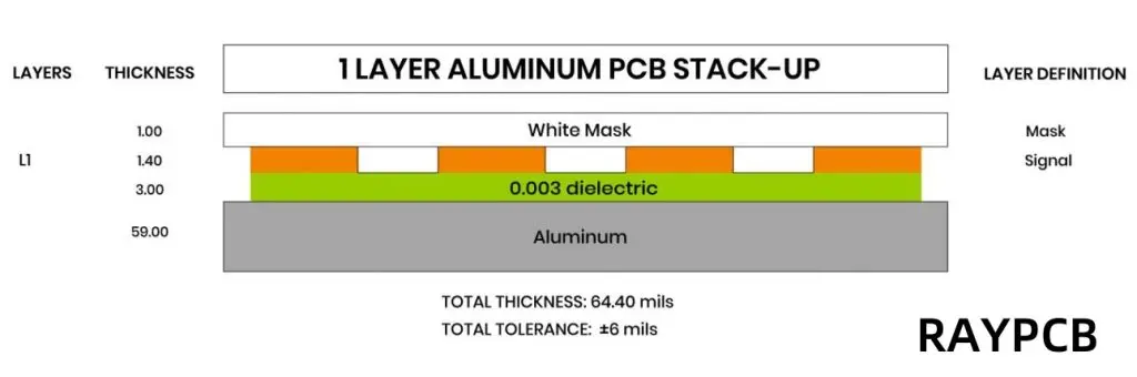
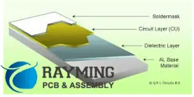
An Aluminum PCB Stackup refers to the layered construction of a printed circuit board that incorporates an aluminum base layer. This structure typically consists of three main components:
Metal Base Layer (Aluminum Core): This forms the foundation of the PCB, providing mechanical support and excellent thermal conductivity.
Dielectric Insulating Layer: A thin layer of thermally conductive yet electrically insulating material that separates the aluminum core from the copper circuitry.
Copper Circuitry Layer: The topmost layer where electronic components are mounted and interconnected.
Comparison to Traditional FR4 Stackups
Unlike traditional FR4 (Flame Retardant 4) stackups that use a fiberglass-reinforced epoxy laminate as the base material, Aluminum PCB Stackups leverage the superior thermal properties of aluminum. This fundamental difference results in significantly improved heat dissipation capabilities, making Aluminum PCB Stackups ideal for high-power applications.
Key Benefits of Aluminum PCB Stackups
Superior Thermal Conductivity
The standout feature of Aluminum PCB Stackups is their exceptional thermal conductivity. The aluminum core acts as a built-in heat sink, efficiently spreading and dissipating heat generated by electronic components. This property is particularly valuable in applications where thermal management is critical, such as high-power LED lighting or automotive electronics.
Enhanced Mechanical Durability
Aluminum’s inherent strength and rigidity contribute to the overall durability of the PCB. This increased mechanical stability helps protect sensitive components from vibration and physical stress, making Aluminum PCB Stackups well-suited for rugged environments.
Lightweight and Compact Design
Despite its strength, aluminum is relatively lightweight compared to other metals. This characteristic allows for the creation of robust yet lightweight PCBs, which is particularly advantageous in applications where weight is a concern, such as aerospace or portable electronics.
Cost-effectiveness for High-Power Applications
While the initial cost of Aluminum PCB Stackups may be higher than traditional FR4 boards, they often prove more cost-effective in high-power applications. The improved thermal management can reduce or eliminate the need for additional cooling solutions, potentially lowering overall system costs.
Challenges in Designing an Aluminum PCB Stackup
Managing Differential Thermal Expansion
One of the primary challenges in designing Aluminum PCB Stackups is managing the differential thermal expansion between the aluminum core and other materials in the stackup. As temperature fluctuates, materials expand and contract at different rates, which can lead to stress and potential delamination if not properly addressed.
Maintaining Signal Integrity at High Frequencies
While Aluminum PCB Stackups excel in thermal management, they present unique challenges for signal integrity, especially at high frequencies. The proximity of the conductive aluminum layer to the signal traces can affect impedance and introduce unwanted capacitance, requiring careful design considerations.
Layer Adhesion and Material Compatibility
Ensuring strong adhesion between the aluminum core, dielectric layer, and copper circuitry is crucial for the longevity and reliability of the PCB. Selecting compatible materials and employing appropriate manufacturing processes are essential to prevent delamination and ensure the PCB’s long-term performance.
Thermal Conductivity Considerations
Role of the Dielectric Layer’s Thermal Conductivity
The dielectric layer plays a crucial role in the thermal performance of an Aluminum PCB Stackup. While it must provide electrical isolation, it should also facilitate heat transfer from the copper layer to the aluminum core. Selecting a dielectric material with high thermal conductivity is key to maximizing the stackup’s heat dissipation capabilities.
Thickness of the Aluminum Core and Heat Dissipation
The thickness of the aluminum core directly impacts the PCB’s ability to spread and dissipate heat. A thicker core generally provides better thermal performance but comes at the cost of increased weight and potentially higher manufacturing complexity. Designers must carefully balance these factors based on the specific requirements of their application.
Examples: Applications in LED Lighting, Automotive, and Power Electronics
Aluminum PCB Stackups find extensive use in applications requiring efficient thermal management:
LED Lighting: High-power LED modules benefit from the enhanced heat dissipation, allowing for brighter and more reliable lighting solutions.
Automotive Electronics: Under-hood electronics and LED headlights leverage Aluminum PCB Stackups to withstand high temperatures and vibrations.
Power Electronics: Inverters, motor drives, and power supplies use Aluminum PCB Stackups to manage the heat generated by high-current components.
Maintaining consistent impedance throughout the PCB is crucial for signal integrity, especially in high-speed digital and RF applications. The presence of the aluminum layer can affect impedance characteristics, requiring careful design and potentially the use of impedance-controlled dielectric materials.
Effects of the Dielectric Constant on Signal Propagation
The dielectric constant of the insulating layer influences signal propagation speed and can impact timing in high-speed circuits. Designers must consider this factor when selecting materials and determining trace geometries to ensure proper signal timing and minimize reflections.
Mitigating Signal Loss and Cross-talk in Multilayer Aluminum PCBs
As with traditional PCBs, multilayer Aluminum PCB Stackups must address signal loss and cross-talk issues. The proximity of the aluminum layer can exacerbate these problems, necessitating careful layer stackup planning, appropriate use of ground planes, and strategic trace routing to maintain signal integrity.
Common Aluminum PCB Stackup Configurations
Aluminum PCB LAYER
Single-sided Aluminum PCB Stackup
The simplest configuration consists of an aluminum base, a dielectric layer, and a single copper layer for circuitry. This design is cost-effective and suitable for applications with straightforward thermal requirements and low complexity.
Double-sided Aluminum PCB Stackup
This configuration adds a second copper layer on the opposite side of the aluminum core, separated by another dielectric layer. It offers increased routing flexibility and can accommodate more complex circuits while maintaining excellent thermal properties.
Multilayer Aluminum PCB Designs
For applications requiring higher complexity, multilayer Aluminum PCB Stackups can be created. These designs typically involve additional dielectric and copper layers built up on one or both sides of the aluminum core. Careful consideration must be given to thermal vias and layer arrangement to maintain optimal heat dissipation.
Hybrid Structures: Combining FR4 and Aluminum Layers
Some designs benefit from a hybrid approach, combining the thermal advantages of aluminum with the cost-effectiveness and familiarity of FR4. These stackups might feature an aluminum core with FR4 layers built up on one or both sides, offering a balance between thermal performance and traditional PCB design techniques.
Material Selection for Optimal Performance
Choosing the Right Dielectric Material
Selecting the appropriate dielectric material is crucial for balancing thermal conductivity and signal integrity. Materials like ceramic-filled epoxy offer high thermal conductivity but may have higher dielectric constants, affecting signal propagation. Conversely, materials with lower dielectric constants might not provide optimal thermal performance.
Copper Thickness Considerations
The thickness of the copper layers affects both electrical and thermal performance. Thicker copper can carry higher currents and aid in heat spreading but may complicate fine-pitch routing and impedance control. Designers must balance these factors based on their specific application requirements.
Aluminum Alloy Types and Their Impact
Different aluminum alloys offer varying thermal, mechanical, and cost characteristics. Common choices include Alloy 1050A for general applications and Alloy 6061 for improved strength. The selection of aluminum alloy can impact the overall performance and cost of the Aluminum PCB Stackup.
Best Practices for Designing an Effective Aluminum PCB Stackup
Aluminum PCB Properties
Thermal Simulation During Design
Utilizing thermal simulation tools during the design phase is crucial for optimizing heat dissipation. These simulations can help identify hotspots, validate cooling strategies, and ensure that the Aluminum PCB Stackup meets the thermal requirements of the application.
Via Design and Thermal Vias
Strategic placement of vias, especially thermal vias, is essential for efficient heat transfer in multilayer designs. Thermal vias provide direct paths for heat to travel from outer layers to the aluminum core, improving overall thermal performance.
Balancing Cost, Performance, and Manufacturability
While Aluminum PCB Stackups offer superior thermal performance, they can be more expensive and challenging to manufacture than traditional PCBs. Designers must carefully balance these factors, considering the entire system cost and performance requirements when deciding on the optimal stackup configuration.
Applications of Aluminum PCB Stackups
High-power LED Modules
Aluminum PCB Stackups are widely used in high-power LED applications, from street lighting to automotive headlights. The efficient heat dissipation allows for higher LED density and brightness while ensuring long-term reliability.
Automotive Electronics
The automotive industry leverages Aluminum PCB Stackups for various applications, including engine control units, LED lighting, and power converters. The combination of thermal management and mechanical durability makes them ideal for the harsh automotive environment.
Industrial Power Equipment
Industrial motor drives, inverters, and power supplies benefit from the high current-carrying capacity and thermal performance of Aluminum PCB Stackups. These attributes enable more compact and efficient power electronics designs.
RF and Microwave Devices
Despite the challenges in maintaining signal integrity, carefully designed Aluminum PCB Stackups find use in RF and microwave applications. The thermal benefits can outweigh the design complexities in high-power RF amplifiers and transmitters.
Future Trends in Aluminum PCB Stackups
Advances in Dielectric Materials
Ongoing research into advanced dielectric materials promises to further improve the thermal and electrical performance of Aluminum PCB Stackups. Materials with higher thermal conductivity and lower dielectric constants will enable even more efficient designs.
Innovations in Multilayer Aluminum Stackups
As demand for higher complexity circuits with excellent thermal management grows, we can expect innovations in multilayer Aluminum PCB Stackup designs. This may include novel layer arrangements and improved manufacturing techniques to optimize both thermal and electrical performance.
Integration with Flexible and Hybrid PCB Technologies
The future may see increased integration of Aluminum PCB Stackups with flexible and rigid-flex technologies, combining the thermal benefits of aluminum with the versatility of flexible circuits. This could open up new possibilities in wearable electronics and other applications requiring both flexibility and thermal management.
Conclusion
Aluminum PCB Stackups represent a significant advancement in PCB technology, offering a powerful solution to the dual challenges of thermal management and signal integrity. By leveraging the superior thermal properties of aluminum while carefully addressing the unique design considerations, engineers can create high-performance PCBs capable of meeting the demands of modern electronics.
As we’ve explored throughout this article, the key to success with Aluminum PCB Stackups lies in understanding their unique characteristics and applying best practices in design and material selection. Whether it’s for high-power LEDs, automotive electronics, or cutting-edge RF devices, a well-designed Aluminum PCB Stackup can provide the perfect balance of thermal conductivity and reliable signal performance.
As technology continues to advance, we can expect further innovations in Aluminum PCB Stackup designs, materials, and manufacturing processes. These developments will undoubtedly expand the applications and capabilities of this versatile technology, solidifying its place as a cornerstone of modern electronic design.
FAQs about Aluminum PCB Stackup
What makes Aluminum PCB Stackups different from standard PCBs? Aluminum PCB Stackups feature an aluminum core that provides superior thermal conductivity compared to traditional FR4 PCBs. This makes them ideal for applications requiring efficient heat dissipation.
Can multilayer Aluminum PCBs maintain high signal integrity? Yes, with careful design considerations. While the aluminum layer can affect signal propagation, proper stackup planning, material selection, and layout techniques can ensure high signal integrity in multilayer designs.
How does the aluminum core thickness affect PCB performance? A thicker aluminum core generally improves thermal performance by providing better heat spreading. However, it also increases weight and can affect manufacturing complexity, so the thickness must be balanced with other design requirements.
Are Aluminum PCB Stackups suitable for all types of electronic designs? While Aluminum PCB Stackups excel in high-power and thermally demanding applications, they may not be necessary or cost-effective for all designs. They are most beneficial in scenarios where thermal management is a critical concern.
How do you address the differential thermal expansion in Aluminum PCB Stackups? Careful material selection, appropriate layer thicknesses, and strategic use of vias can help manage differential thermal expansion. Some designs may also incorporate stress-relief features to minimize the impact of thermal cycling.
In the realm of high-frequency circuit design, the precise control of transmission line characteristics is crucial for optimal performance. Centered stripline devices, a popular choice in many RF and microwave applications, require careful consideration of line widths to achieve desired characteristic impedances. This article delves into the intricacies of line width determination for centered stripline devices using Rogers Corporation’s RT/duroid high frequency laminates, a family of materials renowned for their excellent electrical and mechanical properties.
Powered By EmbedPress
Understanding Centered Stripline Technology
Centered stripline is a type of planar transmission line where a flat conductor is sandwiched between two ground planes, with dielectric material filling the spaces. This configuration offers several advantages, including:
Reduced radiation losses
Better isolation from external electromagnetic interference
Lower dispersion, allowing for wider bandwidth operation
Improved predictability of electrical characteristics
The key parameters that influence the characteristic impedance of a centered stripline include:
Rogers Corporation‘s RT/duroid laminates are widely used in the RF and microwave industry due to their excellent electrical and mechanical properties. These materials offer:
The calculation of line widths for centered stripline devices involves complex electromagnetic equations. However, several approximations and design tools are available to simplify this process. One commonly used approximation for the characteristic impedance (Z0) of a centered stripline is:
Z0 = (60 / √εr) * ln(4b / (0.67π(0.8w + t)))
Where:
Z0 is the characteristic impedance in ohms
εr is the dielectric constant of the substrate
b is half the thickness between ground planes
w is the width of the conductor
t is the thickness of the conductor
To determine the line width for a given impedance, this equation must be solved iteratively or through the use of specialized design software.
Line Width Variations Across RT/duroid Materials
Let’s examine how line widths vary for different characteristic impedances across various RT/duroid materials. We’ll consider a standard 50Ω impedance as well as 25Ω and 75Ω for comparison.
RT/duroid 5870 (εr = 2.33)
50Ω line: Approximately 1.37 mm wide
25Ω line: Approximately 3.56 mm wide
75Ω line: Approximately 0.76 mm wide
RT/duroid 5880 (εr = 2.20)
50Ω line: Approximately 1.42 mm wide
25Ω line: Approximately 3.68 mm wide
75Ω line: Approximately 0.79 mm wide
RT/duroid 6002 (εr = 2.94)
50Ω line: Approximately 1.15 mm wide
25Ω line: Approximately 3.00 mm wide
75Ω line: Approximately 0.64 mm wide
RT/duroid 6006 (εr = 6.15)
50Ω line: Approximately 0.72 mm wide
25Ω line: Approximately 1.87 mm wide
75Ω line: Approximately 0.40 mm wide
RT/duroid 6010LM (εr = 10.2)
50Ω line: Approximately 0.52 mm wide
25Ω line: Approximately 1.35 mm wide
75Ω line: Approximately 0.29 mm wide
Note: These values are approximate and assume a standard dielectric thickness and conductor thickness. Actual values may vary based on specific design parameters and manufacturing tolerances.
Factors Affecting Line Width Calculations
Several factors can influence the accuracy of line width calculations and the resulting impedance:
Frequency dependence: At higher frequencies, the effective dielectric constant may change, affecting the required line width.
Manufacturing tolerances: Variations in dielectric thickness, conductor width, and conductor thickness can all impact the final impedance.
Surface roughness: The roughness of the conductor surface can affect the effective conductor thickness and, consequently, the impedance.
Temperature effects: Changes in temperature can alter the dielectric constant and dimensions of the materials, affecting impedance.
Proximity effects: The presence of nearby conductors or ground planes can influence the effective impedance of the line.
Edge coupling: In closely spaced parallel lines, edge coupling can affect the characteristic impedance.
Design Considerations for Centered Stripline Devices
When designing centered stripline devices using RT/duroid laminates, consider the following:
Impedance matching: Ensure proper impedance matching throughout the circuit to minimize reflections and maximize power transfer.
Tolerance analysis: Account for manufacturing tolerances in your design to ensure that the final product meets specifications.
Thermal management: Consider the thermal properties of the chosen RT/duroid material and design appropriate heat dissipation methods if necessary.
Mechanical stability: Evaluate the mechanical properties of the laminate to ensure it can withstand the intended operating conditions.
Cost considerations: Balance performance requirements with cost constraints when selecting materials and designing the layout.
Manufacturability: Design with manufacturability in mind, considering factors such as minimum line widths and spacing that can be reliably produced.
Advanced Techniques for Precise Impedance Control
To achieve more precise control over impedance in centered stripline devices, consider these advanced techniques:
Electromagnetic field simulation: Use advanced EM simulation software to model the entire structure and optimize line widths for target impedances.
Compensated line structures: Implement compensated line structures to account for manufacturing variations and achieve tighter impedance control.
Laser trimming: Use laser trimming techniques to fine-tune line widths and achieve extremely precise impedances post-manufacture.
Multi-layer designs: Explore multi-layer stripline designs to achieve more complex impedance profiles and routing options.
Impedance-controlled fabrication: Work with PCB manufacturers that specialize in impedance-controlled fabrication to ensure tight tolerances.
Conclusion
The determination of line widths for various characteristic impedances in centered stripline devices using RT/duroid high frequency laminates is a critical aspect of RF and microwave circuit design. By understanding the relationships between material properties, line geometries, and impedance, designers can create high-performance circuits that meet stringent electrical requirements.
The choice of RT/duroid material significantly impacts the required line widths for a given impedance, with higher dielectric constant materials generally requiring narrower lines. This relationship allows designers to balance factors such as circuit size, performance, and manufacturability when selecting materials and designing layouts.
As the demand for high-frequency applications continues to grow, the ability to precisely control impedance in transmission lines becomes increasingly important. By leveraging the excellent properties of RT/duroid laminates and employing advanced design and manufacturing techniques, engineers can push the boundaries of what’s possible in RF and microwave circuit design.
Ultimately, successful implementation of centered stripline devices in RT/duroid laminates requires a holistic approach that considers electrical, mechanical, thermal, and manufacturing aspects. By carefully balancing these factors and utilizing the techniques and considerations outlined in this article, designers can create robust, high-performance circuits that meet the demanding requirements of modern RF and microwave applications.
Welcome to the world of ESP32! If you’re stepping into the exciting realm of Internet of Things (IoT) and embedded systems, you’ve come to the right place. This comprehensive guide will walk you through everything you need to know about the ESP32, from its basic features to programming tips and beginner-friendly projects.
What is the ESP32?
The ESP32 is a powerful, low-cost microcontroller that has taken the maker community by storm. It’s the successor to the popular ESP8266 and packs a punch with its dual-core processor, built-in Wi-Fi and Bluetooth capabilities, and extensive GPIO options. Whether you’re building a smart home device, a wearable gadget, or an industrial sensor network, the ESP32 provides a versatile platform for your projects.
Why is it so popular for IoT and embedded projects?
The ESP32’s popularity stems from its perfect balance of features, cost, and ease of use. Here’s why makers and professionals alike love it:
Powerful processing: Dual-core processor up to 240MHz
Low power consumption: Ideal for battery-operated devices
Rich peripherals: ADC, DAC, touch sensors, and more
Affordable: High-end features at a budget-friendly price
Strong community support: Abundant resources and libraries
What this guide covers
In this guide, we’ll dive deep into the ESP32, covering everything from basic setup to advanced programming tips. You’ll learn about the ESP32’s pinout, how to set up your development environment, and how to bring your ideas to life with practical projects. Whether you’re a complete beginner or looking to expand your ESP32 skills, this guide has something for everyone.
Let’s embark on this exciting journey into the world of ESP32!
The ESP32 is the successor to the widely popular ESP8266, both developed by Espressif Systems. While the ESP8266 revolutionized the IoT landscape with its low-cost Wi-Fi capabilities, the ESP32 takes it a step further by addressing many of its predecessor’s limitations and adding new features.
Introduced in 2016, the ESP32 quickly gained traction in the maker community and professional circles alike. Its combination of powerful processing, wireless connectivity, and affordability made it an instant hit for a wide range of applications.
Key Features
The ESP32 boasts an impressive array of features that set it apart:
Dual-core processor: Two Xtensa 32-bit LX6 microprocessors that can be controlled separately
Clock speed: Up to 240 MHz
Wi-Fi: 2.4 GHz Wi-Fi (802.11 b/g/n)
Bluetooth: Bluetooth v4.2 BR/EDR and BLE (Bluetooth Low Energy)
Low power modes: Deep sleep mode consuming only 10µA
Popular Variants
The ESP32 comes in several variants to suit different project needs:
ESP32-WROOM: The most common module, featuring Wi-Fi and Bluetooth
ESP32-WROVER: Similar to WROOM but with additional PSRAM
ESP32-CAM: Includes a camera module, perfect for video streaming projects
ESP32-S2: A single-core variant with enhanced security features
ESP32-C3: RISC-V based variant with Wi-Fi and Bluetooth LE
Each variant has its strengths, making the ESP32 family versatile enough to cater to a wide range of project requirements.
ESP32 Pinout Overview
Understanding the ESP32’s pinout is crucial for connecting sensors, actuators, and other components to your projects. Let’s break down the most important pins and their functions.
Standard Pinout Diagram
[Insert image of ESP32 pinout diagram here]
Important Pins Explained
Power Pins
3V3: 3.3V power output
GND: Ground
VIN: Input voltage (5V typically)
GPIO (General Purpose Input/Output)
The ESP32 has up to 36 GPIO pins, but not all are available on every module. Some key points:
GPIO 0-39 are available (with some exceptions)
Some pins have special functions (e.g., GPIO 0 is used for booting)
GPIO 6-11 are typically used for connecting the onboard flash, avoid using these
Be aware of the default boot states of pins to prevent unintended behavior
Understanding these pin functions and limitations will help you design your projects more effectively and avoid common pitfalls when working with the ESP32.
Setting Up Your ESP32 for the First Time
Getting started with the ESP32 is straightforward, but there are a few key steps to follow. Let’s walk through the process of setting up your development environment.
What You Need
ESP32 development board (e.g., ESP32-WROOM or ESP32-DevKitC)
void setup() { Serial.begin(115200); WiFi.begin(ssid, password); while (WiFi.status() != WL_CONNECTED) { delay(1000); Serial.println("Connecting to WiFi..."); } Serial.println("Connected to WiFi"); Serial.print("IP address: "); Serial.println(WiFi.localIP());
server.on("/", handleRoot); server.begin(); Serial.println("HTTP server started"); }
void loop() { server.handleClient(); }
void handleRoot() { String html = "<html><body><h1>ESP32 Web Server</h1><p>Hello from ESP32!</p></body></html>"; server.send(200, "text/html", html); }
3. Basic Bluetooth Communication
Implement a simple Bluetooth Low Energy (BLE) server:
pCharacteristic->setValue("Hello World"); pService->start(); BLEAdvertising *pAdvertising = BLEDevice::getAdvertising(); pAdvertising->addServiceUUID(SERVICE_UUID); pAdvertising->setScanResponse(true); pAdvertising->setMinPreferred(0x06); // functions that help with iPhone connections issue pAdvertising->setMinPreferred(0x12); BLEDevice::startAdvertising(); Serial.println("Characteristic defined! Now you can read it in your phone!"); }
These projects provide a solid foundation for understanding key ESP32 features. As you become more comfortable, you can combine these concepts to create more complex and interesting applications
Programming Tips and Best Practices
ESP32 Programming Circuit
To make the most of your ESP32 projects, consider these programming tips and best practices:
Using Deep Sleep to Save Power
The ESP32’s deep sleep mode is crucial for battery-operated projects. Here’s how to implement it:
#define uS_TO_S_FACTOR 1000000 // Conversion factor for micro seconds to seconds #define TIME_TO_SLEEP 5 // Time ESP32 will go to sleep (in seconds)
void loop() { if (WiFi.status() != WL_CONNECTED) { Serial.println("Reconnecting to WiFi..."); WiFi.disconnect(); WiFi.reconnect(); delay(5000); } // Your main code here }
OTA (Over-the-Air) Updates Basics
OTA updates allow you to upload new code to your ESP32 wirelessly:
The ESP32 is a powerful and versatile microcontroller that opens up a world of possibilities for IoT and embedded projects. This guide has covered the basics of getting started with the ESP32, from understanding its pinout to programming your first projects.
We encourage you to try out the projects we’ve discussed and experiment with your own ideas. The ESP32’s flexibility makes it an excellent platform for learning and innovation. As you grow more comfortable with the basics, you can explore more advanced topics like:
Using FreeRTOS for multitasking
Implementing Micropython on ESP32
Creating mesh networks with ESP-NOW
Integrating ESP32 with cloud platforms like AWS IoT or Google Cloud IoT
Remember, the best way to learn is by doing. Start small, build on your successes, and don’t be afraid to ask for help in the ESP32 community. Happy coding!
FAQ: Quick Answers for ESP32 Beginners
Q: Can ESP32 run on 5V? A: While the ESP32 chip operates at 3.3V, many development boards have a voltage regulator that allows you to power them with 5V via USB or VIN pin.
Q: How much memory does ESP32 have? A: The typical ESP32 has 520 KB of SRAM and 448 KB of ROM. Some variants may have different amounts.
Q: Can ESP32 connect to 5GHz Wi-Fi? A: No, the standard ESP32 only supports 2.4GHz Wi-Fi. Some newer variants like the ESP32-C6 support 5GHz.
Q: How many GPIO pins does ESP32 have? A: The ESP32 chip has up to 36 GPIO pins, but the number available on development boards may vary.
Q: Can ESP32 run Arduino code? A: Yes, the ESP32 can be programmed using the Arduino IDE and most Arduino libraries.
While the ESP8266 is still a capable and cost-effective option for simpler projects, the ESP32’s additional features and processing power make it the better choice for more complex applications, especially those requiring Bluetooth or advanced GPIO functionality.
In the world of Printed Circuit Board (PCB) design and manufacturing, seamless communication between designers and fabricators is crucial. As the complexity of electronic designs increases, so does the need for more comprehensive and error-free data formats. Enter KiCad’s ODB++ export functionality – a game-changing feature that’s revolutionizing how open-source PCB designs transition from concept to reality. This article delves into the intricacies of KiCad’s ODB++ export, exploring its significance in modern PCB manufacturing workflows and how it’s bridging the gap between design and production.
Introduction
The journey from a PCB design to a physical board involves multiple steps, each critical to the final product’s quality and functionality. Traditionally, this process relied heavily on Gerber files – a long-standing industry standard for communicating PCB design data. However, as designs grow more complex, the limitations of Gerber files become increasingly apparent.
KiCad, a popular open-source electronic design automation (EDA) software, has been at the forefront of addressing these challenges. With its recent introduction of ODB++ export capabilities, KiCad is not just keeping pace with industry trends – it’s setting new standards for open-source PCB design tools.
This article aims to explore how KiCad’s ODB++ export enhances the PCB manufacturing process, offering insights into its implementation, benefits, and best practices for designers and manufacturers alike.
ODB++ (Open Database++) is a proprietary PCB manufacturing data exchange format developed by Valor Computerized Systems, now part of Siemens Digital Industries Software. Introduced in the 1990s, ODB++ was designed to address the limitations of traditional Gerber files by providing a more comprehensive and intelligent data format for PCB manufacturing.
Why ODB++ Matters
Unlike traditional Gerber files, which primarily contain 2D image data of PCB layers, ODB++ offers a richer, more complete representation of the PCB design. This comprehensive approach includes:
The result is a single, cohesive package that contains all the information needed to manufacture a PCB, reducing the chances of misinterpretation or data loss between design and production stages.
Key Benefits of ODB++ in PCB Manufacturing
Fewer Errors: By providing a more complete dataset, ODB++ reduces the likelihood of miscommunication or missing information, leading to fewer manufacturing errors.
Easier CAM Processing: Computer-Aided Manufacturing (CAM) systems can directly interpret ODB++ data, streamlining the pre-production process and reducing manual intervention.
Improved Communication: ODB++ facilitates clearer communication between designers and manufacturers, as all relevant information is contained in a single, standardized format.
Time and Cost Savings: With reduced errors and streamlined processes, ODB++ can lead to faster turnaround times and lower overall production costs.
KiCad’s Evolution Toward Professional Manufacturing Support
Background on KiCad’s Capabilities
KiCad has long been a favorite among hobbyists and professionals alike for its powerful, free, and open-source approach to PCB design. Historically, KiCad has supported standard output formats like Gerber and Excellon drill files, which have been the industry norm for decades.
Challenges with Traditional Gerber + Drill Files
While Gerber files have served the industry well, they come with limitations:
Multiple Files: A complete Gerber package typically includes separate files for each PCB layer, drill data, and often additional documentation.
Limited Intelligence: Gerber files essentially describe PCB layers as images, lacking inherent information about connectivity or component properties.
Potential for Errors: Managing multiple files increases the risk of missing or mismatched data during the handoff to manufacturers.
Growing Demand for ODB++ in Open-Source Workflows
As more professional designers and manufacturers adopt open-source tools like KiCad, the demand for industry-standard outputs like ODB++ has grown. This push reflects a broader trend in the industry towards more integrated, data-rich design-to-manufacturing workflows.
KiCad’s ODB++ Implementation
KiCad introduced ODB++ export capabilities in version 6.0, with continued improvements in subsequent releases. This addition marked a significant step in KiCad’s evolution, aligning it more closely with commercial EDA tools and professional manufacturing requirements.
Open Your PCB Project: Ensure your design is finalized and ready for manufacturing.
Access the Export Menu:
Navigate to “File” > “Export” > “ODB++”
Alternatively, use the shortcut Ctrl+Alt+O (Windows/Linux) or Cmd+Alt+O (Mac)
Configure Export Settings:
Choose the output directory
Select layers to include
Specify netlist and drill file options
Review and Confirm: Double-check your settings before initiating the export process.
Export: Click “Export” to generate the ODB++ files.
Overview of Export Options and Settings
Layers: Select which PCB layers to include in the ODB++ output.
Netlist: Choose to include detailed netlist information.
Drill Files: Specify drill file formats and options.
Component Placement: Include data on component positions and orientations.
Design Rules: Option to include DRC (Design Rule Check) information.
Practical Tips for Clean ODB++ Export
Validate Your Design: Run DRC checks before exporting to ensure your design is error-free.
Use Consistent Units: Ensure all measurements in your design use consistent units to avoid conversion issues.
Check Layer Stack-up: Verify that your layer stack-up is correctly defined before export.
Review Component Properties: Ensure all components have correct footprints and attributes assigned.
Common Mistakes to Avoid
Incomplete Layer Selection: Forgetting to include critical layers in the export.
Ignoring DRC Errors: Exporting without resolving design rule violations.
Outdated Libraries: Using old component libraries that may not align with current manufacturing standards.
Neglecting Mechanical Layers: Forgetting to include important mechanical information like board outlines or assembly notes.
Why Use ODB++ with KiCad?
ODB++ Vs. Gerber
Advantages over Traditional Gerber Exports
Consolidated Package: ODB++ provides all necessary manufacturing data in a single, organized structure, reducing the risk of missing files.
Enhanced Data Intelligence: ODB++ includes detailed information about components, nets, and design rules, enabling more intelligent processing by manufacturers.
Improved Accuracy: The comprehensive nature of ODB++ data reduces the chance of misinterpretation or errors during the manufacturing process.
Faster Turnaround: With more complete data upfront, manufacturers can often process ODB++ files more quickly, potentially leading to faster production times.
Better Error Checking and Validation
ODB++ allows for more thorough automated checks at the manufacturing stage, catching potential issues that might be missed with Gerber files alone. This can include:
The comprehensive nature of ODB++ often results in fewer queries from manufacturers, streamlining the production process. This reduction in communication cycles can lead to:
Faster time-to-market
Fewer opportunities for miscommunication
Reduced overall project stress
Real-World Feedback from Manufacturers
Many PCB manufacturers report preferring ODB++ files for several reasons:
Ease of Use: ODB++ files are often easier to import and process in modern CAM systems.
Reduced Pre-Production Time: The completeness of ODB++ data often results in less time spent on pre-production setup and checks.
Higher Confidence: Manufacturers often express higher confidence in the accuracy of ODB++ data compared to traditional Gerber files.
Limitations and Considerations
ODB++ Export Maturity in KiCad
While KiCad’s ODB++ export functionality is a significant advancement, it’s important to note that it’s still a relatively new feature. As with any software feature, there may be occasional bugs or limitations:
Ongoing Development: The KiCad team continues to refine and improve ODB++ export capabilities with each release.
Community Feedback: Users are encouraged to report any issues or inconsistencies they encounter to help improve the feature.
Version Compatibility: Always check the KiCad release notes for the latest information on ODB++ export capabilities and any known issues.
Compatibility Considerations
While ODB++ is growing in popularity, it’s not universally accepted by all PCB manufacturers:
Check with Your Manufacturer: Always verify that your chosen PCB fabricator accepts and can process ODB++ files.
Gerber as Backup: Consider providing both ODB++ and traditional Gerber files to ensure compatibility with a wider range of manufacturers.
Growing Acceptance: More PCB fabricators are adding ODB++ support, but it’s not yet universal.
When to Stick with Traditional Outputs
There are scenarios where traditional Gerber files might still be preferable:
Simple Designs: For very simple PCBs, the additional complexity of ODB++ might not offer significant advantages.
Manufacturer Preference: Some PCB fabricators might still prefer or only accept Gerber files.
Legacy Systems: If you’re working with older manufacturing systems or processes, Gerber files might be more compatible.
Best Practices for Smooth Handoff to PCB Manufacturers
Checklist for Validating ODB++ Files Before Sending
Layer Completeness: Ensure all necessary layers are included in the ODB++ package.
Netlist Verification: Double-check that the netlist in the ODB++ file matches your design intent.
Component Placement: Verify that all components are correctly placed and oriented.
Drill File Accuracy: Confirm that all drill data is accurate and complete.
Design Rule Compliance: Run a final DRC check to ensure all design rules are met.
Recommended Tools for Previewing ODB++ Outputs
ODB++ Viewer: Use specialized ODB++ viewing software to inspect your export.
CAM350: A professional tool that can open and analyze ODB++ files.
CircuitCAM: Another professional option for viewing and validating ODB++ data.
Online Viewers: Some PCB manufacturers offer online tools to preview and check ODB++ files before submission.
Communicating with Your PCB Fab About ODB++ Capabilities
Early Inquiry: Reach out to your manufacturer early in the design process to discuss their ODB++ capabilities.
Specification Alignment: Ensure your ODB++ export settings align with your manufacturer’s requirements.
Version Information: Provide information about the KiCad version used for the export, as this can be helpful for troubleshooting.
Feedback Loop: Establish a clear channel for feedback from the manufacturer regarding the ODB++ files.
Conclusion
KiCad’s support for ODB++ export represents a significant leap forward in bridging the gap between open-source PCB design and professional manufacturing processes. By providing a more comprehensive and intelligent data format, KiCad is empowering designers to communicate their intentions more clearly and efficiently with manufacturers.
The introduction of ODB++ export in KiCad not only enhances the software’s capabilities but also elevates the entire open-source PCB design ecosystem. It demonstrates that open-source tools can indeed meet and even exceed industry standards, providing professionals with powerful, cost-effective alternatives to proprietary solutions.
As KiCad continues to evolve and refine its ODB++ export functionality, designers are encouraged to explore this feature alongside traditional Gerber exports. The potential benefits in terms of reduced errors, faster turnaround times, and improved communication with manufacturers make it a valuable addition to any PCB designer’s toolkit.
The ongoing development and improvement of features like ODB++ export in KiCad underscore the software’s commitment to providing cutting-edge, professional-grade tools to the open-source community. As more designers adopt these advanced features and provide feedback, we can expect to see even greater strides in the capabilities and reliability of open-source PCB design tools.
In embracing ODB++ export with KiCad, designers are not just improving their own workflows – they’re contributing to a broader shift in the industry towards more open, efficient, and collaborative PCB design and manufacturing processes.
Yes, KiCad supports ODB++ export starting from version 6.0, with ongoing improvements in subsequent releases.
What’s the difference between ODB++ and Gerber in KiCad?
While Gerber files primarily contain 2D image data of PCB layers, ODB++ provides a more comprehensive package including netlist data, component placement, and manufacturing notes, all in a single, structured format.
Can you edit ODB++ files exported from KiCad?
ODB++ files are not directly editable like Gerber files. They’re intended as a final output for manufacturing. Any changes should be made in the original KiCad design and then re-exported.