Top Soldering Flux Types Compared: Rosin, No-Clean, and Water-Soluble

soldering flux

Introduction

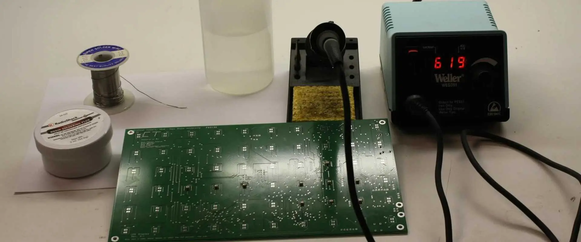
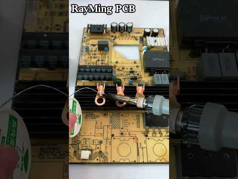
Soldering is an essential skill in electronics, and one of the key components in this process is soldering flux. Whether you’re a hobbyist working on DIY projects or a professional in the electronics industry, understanding the different types of soldering flux can significantly impact the quality and longevity of your work. In this comprehensive guide, we’ll explore the three main types of soldering flux: rosin, no-clean, and water-soluble. We’ll compare their pros and cons, discuss their best uses, and provide you with the knowledge to choose the right flux for your specific needs.

YouTube video

What Is Soldering Flux?

Before diving into the specific types, let’s first understand what soldering flux is and why it’s crucial in the soldering process.

Definition and Purpose

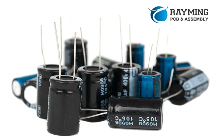
Soldering flux is a chemical cleaning agent used in the soldering process to remove oxides from the metal surfaces being joined. It helps to prevent new oxides from forming during the soldering process, which could weaken the joint.

How Soldering Flux Works

  1. Removes oxidation: Flux chemically cleans the metal surfaces.
  2. Improves wetting: It helps the solder flow more easily across the joint.
  3. Protects from re-oxidation: Flux shields the heated metal from the air, preventing new oxide formation.

Importance in Soldering

Without flux, soldering would be significantly more difficult and less reliable. Flux ensures that the solder can properly adhere to the metals being joined, creating a strong and durable connection.

Rosin Flux: Pros, Cons & Best Uses

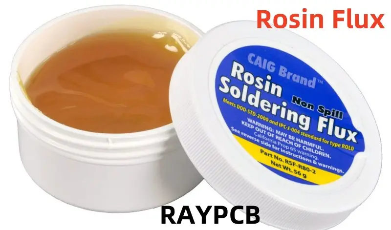
Rosin flux is one of the oldest and most widely used types of soldering flux. It’s derived from pine tree sap and has been a staple in the electronics industry for decades.

Pros of Rosin Flux

  1. Excellent cleaning ability: Effectively removes oxides from metal surfaces.
  2. Low conductivity: Minimal risk of causing electrical shorts.
  3. Stable at room temperature: Easy to store and handle.
  4. Variety of forms: Available in liquid, paste, or core solder form.

Cons of Rosin Flux

  1. Leaves residue: Requires cleaning after soldering.
  2. Can be corrosive: If not cleaned properly, may cause long-term damage.
  3. Fumes during soldering: Can be irritating to some users.

Best Uses for Rosin Flux

  • General electronics repair and assembly
  • Hobby projects
  • Situations where post-soldering cleaning is possible

Read more about:

No-Clean Flux: Pros, Cons & Best Uses

No Clean Flux

No-clean flux has gained popularity in recent years, especially in commercial electronics manufacturing. As the name suggests, it’s designed to not require cleaning after the soldering process.

Pros of No-Clean Flux

  1. No cleaning required: Saves time and reduces the risk of damage during cleaning.
  2. Low residue: Leaves minimal residue after soldering.
  3. Non-corrosive: Safe for long-term use without cleaning.
  4. Suitable for sensitive components: Less risk of damage to delicate parts.

Cons of No-Clean Flux

  1. Less effective cleaning: May not work as well on heavily oxidized surfaces.
  2. Visible residue: Can leave a slight residue that may be visible.
  3. Potential for long-term issues: If used improperly, residue can accumulate over time.

Best Uses for No-Clean Flux

  • High-volume production environments
  • Assemblies with sensitive components
  • Situations where post-soldering cleaning is difficult or impossible

Water-Soluble Flux: Pros, Cons & Best Uses

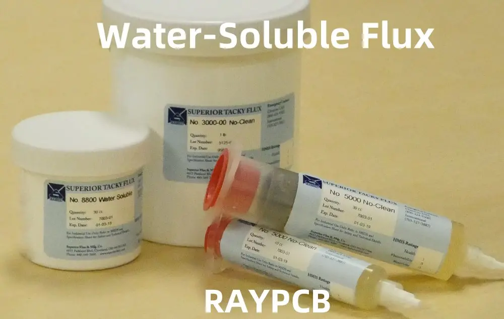
Water-soluble flux offers a balance between the cleaning power of rosin flux and the convenience of no-clean flux. As the name implies, its residues can be cleaned with water.

Pros of Water-Soluble Flux

  1. Powerful cleaning action: Excellent for heavily oxidized surfaces.
  2. Easy to clean: Residues can be removed with water or mild detergent.
  3. Available in various forms: Liquid, paste, or core solder options.
  4. Environmentally friendly: Water-based cleaning reduces solvent use.

Cons of Water-Soluble Flux

  1. Requires prompt cleaning: Can be corrosive if left on the board.
  2. Potential for water damage: If not dried properly, can lead to corrosion.
  3. More complex cleaning process: Requires thorough rinsing and drying.

Best Uses for Water-Soluble Flux

  • Industrial and military applications
  • Situations requiring thorough cleaning
  • When working with heavily oxidized metals

Side-by-Side Comparison Table

To help you quickly compare the three types of soldering flux, here’s a side-by-side comparison table:

FeatureRosin FluxNo-Clean FluxWater-Soluble Flux
Cleaning PowerExcellentGoodExcellent
ResidueModerateMinimalModerate (water-soluble)
Cleaning RequiredYesNoYes (with water)
Corrosion RiskLow (if cleaned)Very LowHigh (if not cleaned)
Ease of UseModerateHighModerate
Best ForGeneral electronicsHigh-volume productionIndustrial applications
EnvironmentalModerate concernLow concernLow concern
CostLow to ModerateModerate to HighModerate

How to Choose the Right Flux

soldering flux

Selecting the appropriate soldering flux is crucial for achieving the best results in your soldering projects. Here are some factors to consider:

1. Type of Project

  • Hobby projects: Rosin flux is often sufficient.
  • Professional electronics: No-clean or water-soluble may be better.
  • High-reliability applications: Water-soluble with thorough cleaning.

2. Cleaning Capabilities

  • Limited cleaning ability: No-clean flux is ideal.
  • Thorough cleaning possible: Rosin or water-soluble can be used.

3. Component Sensitivity

  • Delicate components: No-clean flux is safest.
  • Robust components: Any flux type can be used.

4. Environmental Concerns

  • Eco-friendly option: Water-soluble flux with water cleaning.
  • Minimal waste: No-clean flux.

5. Skill Level

  • Beginners: Rosin flux is forgiving and easy to use.
  • Experienced users: Can take advantage of no-clean or water-soluble benefits.

Safety Tips for Using Flux

While soldering flux is essential for good solder joints, it’s important to use it safely:

  1. Ventilation: Always work in a well-ventilated area to avoid inhaling fumes.
  2. Personal Protective Equipment (PPE): Wear safety glasses and consider using a mask.
  3. Skin Protection: Use gloves when handling flux directly.
  4. Fire Safety: Some flux types are flammable; keep away from open flames.
  5. Storage: Store flux in a cool, dry place away from food and drinks.
  6. Disposal: Follow local regulations for proper disposal of flux and cleaning materials.

Top Recommended Flux Products

Here are some highly-rated soldering flux products for each type:

Rosin Flux

  1. Kester 186 Soldering Flux Pen
  2. MG Chemicals 835-100ML Liquid Rosin Flux

No-Clean Flux

  1. ChipQuik NC191 No-Clean Flux Paste
  2. MG Chemicals 8341 No Clean Flux Pen

Water-Soluble Flux

  1. Kester 2331-ZX Water Soluble Liquid Flux
  2. MG Chemicals 8341-10ML Water Soluble Flux Pen

FAQs About Soldering Flux

Q1: Can I use the same flux for all my soldering projects?

A: While it’s possible, it’s not always ideal. Different projects may benefit from different flux types. For general hobby use, a good rosin flux can cover most needs.

Q2: How do I clean rosin flux residue?

A: Isopropyl alcohol (IPA) is effective for cleaning rosin flux. Use a brush or lint-free cloth dampened with IPA to gently scrub the residue away.

Q3: Is it necessary to remove no-clean flux?

A: No-clean flux is designed to be left on the board. However, in some high-reliability applications, it may still be cleaned for aesthetic or functional reasons.

Q4: Can water-soluble flux damage my electronics if not cleaned properly?

A: Yes, water-soluble flux can be corrosive if left on the board. It’s crucial to clean it thoroughly with water and ensure the board is completely dry afterward.

Q5: How long can I store soldering flux?

A: Most flux has a shelf life of 1-2 years when stored properly in a cool, dry place. Always check the manufacturer’s recommendations.

Conclusion

Choosing the right soldering flux is a crucial step in ensuring successful and reliable solder joints. Each type of flux – rosin, no-clean, and water-soluble – has its own strengths and ideal use cases. By understanding these differences, you can make an informed decision based on your specific needs, whether you’re working on a hobby project or professional electronics assembly.

Remember to always prioritize safety when working with flux, and don’t hesitate to experiment with different types to find what works best for your soldering style and projects. With the right flux and proper technique, you’ll be well on your way to creating strong, reliable solder connections in all your electronic endeavors.

How Does Battery Charger Indicator Work?

battery charge indicator

Overcharging always leads to battery health concerns. It makes them swell or melt over extra charging. However, if this does not take control in time, it may also affect the users too. Moreover, overcharging makes the battery casting too hot, which creates volatile hydrogen in the sealed cells of the battery. Thus, turning them into bad cells. Fortunately, you can easily prevent your batteries from overcharging through battery indicators. This article, however, gives a brief detail about how these battery charger indicators work and how you can make one.

Battery charger indicator refers to a type of device that shows battery status using LCD and LED. This indicator is specifically used to see the left battery level. You can see the battery indicator in the form of bars or dots in smartphones. That perfectly shows the status of the remaining battery present. This battery indicator contains a circuit that determines the device battery over the glowing LED numbers and then shows it over the LCD. 

Heyer first introduced this advanced concept to the people in 1938. His concept simply proposed the idea of a battery level indicator that shows battery percentage. This indicator refers to the amount of voltage and power left in a battery. It uses LEDs and LCD to display the input. It determines the batter level through the glowing number of LEDs and the color simultaneously. Then the LCD displays the output or the battery percentage. However, this battery indicator only uses LM3914 IC that controls the LED and operates the LEDs. Moreover, despite using a controller of LCD and LED, microcontrollers prove best to upgrade the functionality of the circuit.

Battery Charge Indicators

Battery indicators or charger indicators refer to a type of device that shows battery percentage. Also, it shows the status of the battery in accurate visual indication form. Moreover, high-tech devices that need advanced batteries to operate already have built-in battery charger indicators. These devices include computers, tablets, laptops, calculators, smartphones, smartwatches, power banks, some game players, etc. 

Mobile phones also use different types of visuals to show the battery status. Some whose status is in bar graphs. This means the higher the graph, the higher the battery. At the same time, some use percentages to show the status. Moreover, the battery charge indicator does not only show the status of the battery but also the charging mode. This means that some wearable or portable mini devices; show battery charging mode whether it’s charging right now or not. Other than that, it also shows the number of times a device needs to charge fully. This feature is included in smartphones, laptops, smartwatches, and power banks.ย 

Furthermore, battery indicators use lights to tell the high and low status of the battery. An ideal battery system contains an integrated controller. This contains an interchangeable pack of batteries. Thus, this helps the battery indicator to give an accurate result of the battery charging status.

Make A Battery Charge Indicator Circuit

Battery charger indicators can be made through various types of methods. Thus giving the precise status of the batter. Here we have three main and common methods of making mattery indicators. These include

  1. Battery charging indicator circuit in percentage.
  2. Battery indicator circuit with IC LM3914.
  3. A circuit of full charge battery indicator with two transistors.

Components Required

The first circuit needs the following components:

  1. 1 PCB
  2. 5 Resistors of 1k
  3. 1 DC supply of max 15 V
  4. 1 Resistor of 15 k
  5. 1 Resistor of 10k
  6. One resistor of 47k
  7. Some brown and black connecting wires

Steps

The construction of this circuit is divided into four simple steps.

  1. First, insert all the electrical components on the surface of the PCB. This includes all resistors and LEDs. Make sure LEDs connected in series
  2. Once you place all the components over their places. Then start soldering all resistors, LEDs, and wires
  3. Then take brow wire as a positive terminal while black wire as a negative terminal. Solder them over the PCB. However, this power especially connects with the PCB.
  4. In the last, match all the connection points with the diagram or design. Ensure all the connections are made perfectly. Then supply power of 13 V to test the circuits. If they light up, the circuit works fine.

How does It work?

The battery indicator circuit shows the percentage of the battery in ascending form using LEDs. In this, each LED has a specific range of percentages. The first shows 20%, the second 40%, the third 60%, the fourth 80%, and the fifth LED shows 100% battery. Moreover, LEDs glow on different voltage supplies. On the supply of 5 volts, only 2 LEDs glow, while on the supply of 10V, 3 LEDs glow up. However, when the power supply reaches 13 volts, it glows up all the LEDs.

Battery Level Indicator Circuit – LM3914

FULL PCB MANUFACTURING Quote

This type of circuit contains an integral part, an LM3194 Integrated Circuit. This IC works on the supply of analog voltage, which linearly glows the LEDs based on the analog input voltage. Moreover, this circuit does not require the connection of LEDs and resistors in series form, as the IC can transfer the current across all the circuits equally.

Components Required

The construction of this circuit requires the following components

  1. 1 IC LM3914
  2. 1 SPST switch
  3. 1 Battery
  4. 10 LEDs ( 4 yellow, three green, and three red)
  5. 1 Resistor of 3.75Kohm
  6. 1 Resistor of 1.25Kohm
  7. Some connecting wires

Circuit Design

In this circuit, LEDs display the capacity of the battery in dot mode. You may choose the desired mode with an external switch. This external switch must need to connect with IC pin 9. Moreover, connect pin seven and pin 6 to GND using a resistor. This resistor determines the brightness of LEDs. The POT RV1 and R2 or resistor create a circuit of the potential divider. It does not need any external source of power supply as the POT RV1 handles the calibration.

Moreover, utilize different colors of LEDs that help in sowing the status of the batter. This red LED shows low battery status. While green LEDs show fully or almost fully charged batteries. Whereas yellow LEDs help in indicating other statuses of power. Moreover, in this, each LED shows a battery level of 10%.

How To Test & Use?

Firstly, create a connection between the circuit and the battery of 12 Volts. Set the POT RV1 and wait for it to glow. Then increase the DC input voltage gradually and see the glow of LEDs. You can also test the circuit functionality. The first LED shines over a voltage of 1.2v, and the second glow over a voltage of 2.4v. Whereas when the input voltage reaches 12v, it glows up all the LEDs. Moreover, this circuit works over a small input voltage supply. Therefore it may need some tweaks to operate correctly.

Battery Full Charge Indicator Circuit Using Two Transistors

This fully charged battery indicator lights up the LED when the battery is fully charged. Moreover, it does not need many components other than just two transistors.

LED Switching On At Full Charge

The main purpose of this circuit is to light up the LEDs as the battery of the device charges fully. Therefore, to make this circuit, you need to provide desired upper charge status. Then create a setting according to it to make LEDs light up when it crosses the set status.

LED Switching Off At Full Charge

Moreover, this circuit also allows the LEDs to turn off once the battery charges completely. 

How To Set up And Use?

It’s one of the easiest circuit battery indicators to set up. First, set a high level of charging. Then supply the input voltage that must be equal to it. After that, tweak the circuit carefully using the screwdriver so that the LEDs turn off at the desired level. Therefore if the circuit manages the battery of 12v over the charge level of 14.3v, then you may tweak the pre-setting to turn off the LED over 14 volts.

Conclusion

Battery charger indicators also refer to the percentage or level indicator that is the integrated circuit for all the devices that operate on batteries. Without these devices, you may overcharge the device, which leads to damage. Or you may forget to charge the device, which ends up turning off on a very important matter.

Not only do smart devices operate on batteries, but it also serves an important role in remote battery vehicles. It is essential to know the condition of the battery every time so that it wonโ€™t end up stopping in the middle of the road and leading to unwanted accidents. Therefore, these battery indicators help the user to keep track of the battery’s health. 

However, this article shows different ways to make these battery indicator circuits using different types of components. The working principle of these battery indicators must have shown you their significance in battery-operated devices. You can also try to make these indicators on your own, or you can ask manufacturers to make them for your device.

How to Improve Line Efficiency in Electronics? An Ultimate Guide

LINE EFFICIENCY

In the PCBs, the line efficiency refers to the ratio a pick-and-place robot takes to place components over the surface of a PCB, which is divided by SMT assembly staffing time. Line efficiency can be measured with various methods. These include capacity utilization. Compare the production process to the average line efficiency and acceptable production; it gives the capacity utilization value.

Line efficiency plays an integral part in the production and assembly process of PCBs. Therefore, one requires complete knowledge of line efficiency when dealing with production lines. Manufacturers can easily earn greater money if they fasten their assembly process of circuit boards. Whereas if the manufacturer is facing problems with the system and losing efficiency, thus resulting in underproduction. Therefore, in such time they need to identify the root cause of the problem and remove it as quickly as possible.

YouTube video

Formula of Line Efficiency

To calculate the line efficiency while using an SMT line, make sure to consider its efficiency level. According to many experts, the efficiency measurement of SMT seems a bit of a complex process. 

The efficiency formula of the line refers to a P&P machine taking time to place all the components on the PCB, which is divided by the SMT production line time taken for staffing. In simple words, it refers to the positioning time in hours by the staffing time in hours multiplied by 100. This, however, provides a simple, accurate, and clear value of the performance. 

Many manufacturers seem reluctant to utilize the efficiency of production lines instead of SMT lines. Because the efficiency of the production line does not consider time during measurement, this happens because the ratio is based on the actual staffing time instead of optimum time and labor time. Therefore, remember that uncontrollable outside factors affect the productivity level the most. Whereas the demand for the market the PCB assembly volume needs a factory. 

Moreover, one can easily measure the efficiency line number fastly and without effort, as it allows the easy process of calculating SMT time and placement time. The P&P operator needs to take readings of the placement of components. With the help of these recorded readings, one can easily identify the time of placement.ย 

Furthermore, one can also easily measure the time of staff hours if the manager keeps all the records noted and safe in computerized form. Also, even the break time of staff and employees is considered in the staff hours. Therefore, to enhance the efficiency of the line, make sure to keep all records, including the meeting, meals, and breaks of the staff. This ensures all the workers work on the line all the time. 

Thus, this gives an accurate, clear, consistent, and Jones efficiency value of the line. As you know, SMT production line efficiency provides an effective method to measure efficiency and productivity. Hence, use this method from now on to measure your lines.

Improving Line Efficiency in Electronics 

There are a few good methods for improving the efficiency of the production line. Collecting data is considered very important as much as the usage of data matters. Additionally, other than calculating the efficiency of the line, you must find out the factor that affects the efficiency of the line. It helps in analyzing the team’s performance also.

The collected data quality analysis helps in identifying the lagging behavior of productivity. This, however, offers changes and alterations that help to improve overall efficiency. A few possible reasons for productivity lagging include the following. There may be too many operators or not enough operators on the production line. Production lines may contain poor configuration and issues in the management of time. Moreover, the functionality and outdated behavior of the machine and equipment used in the production lines.

Benefits Of Assembly Line Balancing

smt factory

ยท       Reduce Waste

Waiting for waste refers to a type of lean manufacturing waste. This simply refers to any free time that happens during the non-synchronization of operations. For instance, waiting for waste mostly happens when operators wait for material and something else to finish the task. Moreover, equipment downtime also comes in waiting for waste type. It refers to a time when equipment doesn’t work. However, line balancing makes sure that all machines and operators work together to create a balanced work environment. It does not overburden the machine or operator. Therefore, this way, line balancing minimizes downtime. This automatically reduces the waiting waste.

ยท       Reduce Inventory Waste

The inventory waste serves as another waste type. It refers to raw material excess, finished products, or unfinished WIP products. Inventory waste determines the inefficient use of capital. However, line balancing makes the production standardize. This means that one can easily avoid excess inventory or build-ups. It reduces the free time and is sure that only a minimum amount of WIP is left. At the same time, it brings the time of production closer to desired time which guarantees delivery on time.

ยท       Absorb Irregularities

Life balancing minimizes the amount of variation in the production line. However, a balanced line refers to a stable line that has enough flexibility to adapt to any type of change. For instance, if a customer requests changes, the operation must realign fastly with line balancing. Moreover, one can easily produce the impact of the changes on the balanced line. Therefore, it makes it easy to modify an altered line to fix the rate of production.

ยท       Lower Production Cost 

A perfectly balanced line enables the machine and worker to operate in a synchronized way. Operators are not getting paid for just standing idle. Whereas machines also need to operate at their full potential. However, in simple words, it maximizes the capacity of machines and manpower. Such efficiency in the process leads to more profit and lesser costs.


Why Is Line Efficiency A Essential for The PCB Manufacturing Industry?

The PCB manufacturer’s profit depends on several business metrics. These metrics indicate the complex functionality of a production or assembly unit. Line efficiency serves as one of those factors. Line efficiency contains two types of methods to measure the efficiency of the line assembly unit of PCB. These two factors include the Surface-mount line Efficiency and the Production line.

The majority of manufacturers of PCBs tend to use SMT lines because of consistent and precise results. They do not use the production line because of its incompleteness. The ratio of production line efficiency does not contain the optimum time and the labor time. Therefore, it creates various types of challenges for the operators, which directly affects the efficiency of the line. At the same time, SMT production line efficiency serves as the most used metric. It gives correct and easy measurement with recorded staff time. Moreover, the output data to calculate the efficiency of the line needs to go through analysis to find degrading factors. This data helps in finding the lagging behavior of productivity, as we read before. 

Line efficiency refers to an essential business matrix that helps in evaluating the resource output of the assembly. It is incorporated with other factors like ORE and OEE, the overall equipment, and resource effectiveness whilst measuring the efficiency of the production. Identifying the efficiency of the line helps the contract manufacturers to reduce manual labor and enhances the placement of components per line. However, this reduces the risk of any delay in delivery. 

Moreover, manufacturers of PCB tend to adopt diverse manufacturing, which produces multiple products altogether. In such cases, optimizing the production also depends on the time of changeover. Shifting from batches of product one-on-one limits the overall line assembly utilization.

Main SMT Line Machine Efficiency 

The SMT line of PCB assembly contains the following few essential machines and equipment.

ยท       Pick & Place Machine

This P&P machine picks the SMT component and places it accurately over the surface of the PCB using the robotic placement hand. However, the tension in the surface of the solder pulls out the SMD automatically in alignment later in the soldering reflow process to fix little errors in the placement of the components.

ยท       Solder Paste Mixer

The soldering paste mixer, as the name suggests, mixes the paste of solder and powder efficiently and evenly. It helps in making the printing process, reflow, and standardized functions and minimizes the requirement of manual labor.

ยท       Oven

In the SMT line, both oven and reflow differ from each other. The oven bakes the PCBs to remove any type of moisture and comes in the last of an SMT line.

ยท       SMT Loader

The SMT loader places the circuit board in the soldering printing equipment racks automatically.

ยท       Solder Paste Printing Machine

The soldering paste printing device prints the soldering paste to draw off the board. It comes after the P&P device in an SMT Production line.

ยท       Solder Paste Inspection Machine

SPI refers to a Soldering Paste Inspection device. It analyzes the volume, thickness, and area of soldering paste over the surface of the PCB after the soldering printing process.

ยท       Reflow Machine

The reflow machine comes after the P&P machine. It melts the soldering paste between the SMT components and PCB to create a welding connection between them. After that, it cools down the solder paste and solidifies the welding bond.

ยท       AOI

The AOI machine sandwiches the reflow soldering machine in between two AOI. The first machine identifies any type of failures and errors in the placement of components before sending it to reflow. The second AOI checks the errors and failures of soldering after the reflow.

ยท       Docking Station

The docking station provides an intermediate stop between distinct machines of the SMT Production line.

ยท       SMT Unloader

The SMT unloader, as the name suggests, operates in the opposite way of the SMT loader. However, it receives the assembled board and stores it after the soldering reflow process.

Types Of SMT Production Line Efficiency

FULL PCB MANUFACTURING Quote

The design of the SMT line type contains the following details:

  1. One line contains a layout of a single rail P&P machine.
  2. The two-to-one line contains a layout of single or dual-rail P&P machine
  3. Tow-to-one contains the layout of a dual-rail P&P machine
  4. The three-to-one line contains a layout of a single-rail P&P machine
  5. Combination of multiple line layouts.

SMT Line Cost

SMT line contains around 60 to 70% pick and places robots. A large P&P machine that has a capacity of 100,000+CPH costs about $700,000. Whereas P&P with a middle range capacity of 12 to 35,000 CPH costs about $100 to $200,000.

However, the majority of brands usually cost one line of SMT of about $8,000,000. This seems so expensive. Therefore, we introduced high-tech, advanced SMT lines at a lower cost. It provides reliable and high-quality PCB production while keeping the production cost low. 


SMT Line Efficiency Development Trends

SMT production lines have several ongoing trends. Some of them include:

ยท       CIMS Application

CIMS refers to a computerized Incorporated manufacturing system. It basically links the production process and the design to minimize the time that preparation for SMT Production takes.

ยท       Efficiency Improvement

Efficiency is considered as the source of high output. At the same time, SMT lines are continuously obsoleting the human factor. However, to improve efficiency, try to implement a centralized CMS for the whole SMT line.

ยท       Environmental Protection

SMT production lines use materials like glue, solder paste, flux, and packaging material, which lead to environmental pollution. Although, the majority of PCB assemblers and manufacturers have started using an eco-friendly production process. They first identify the source of pollution and analyze how much quantity they use in the process. Then they look for methods to minimize their effect on the surroundings and create an eco-friendly environment. 

ยท       Flexible Production Environment

Internet development and grid IT provide process data control along with data management of products. This improves the functions of SMT lines. Moreover, they help in increasing maintenance management. Thus, eventually, make a flexible data integration production setup for SMT production lines. 

Conclusion 

SMT lines play an important role in the assembly process of Printed Circuit Boards. These SMT lines contain various types of high-tech machines that perform different types of functions. This article has explained all the details that you might need to know regarding SMT production lines. However, if you still have any type of query. Feel free to contact us.

Choose Rayming PCB for Irregular component Soldering Service

Irregular component

Wave soldering is highly important for smooth PCB assemblies, and we all know that. The process is popular among producers due to its quality and benefits. It strongly develops connections between the PCB parts and PCBs so that no harmful and unfavorable conditions would detach the components from PCBs. Wave soldering works on waves that come after each other to connect the components. Wave soldering is an interesting process, and we are going to explain our services besides wave soldering in this post so that you can choose what fits best for you easily!

As you already know, a PCB has a wide range of multiple components. Some are big, while others are small. You need a seasoned firm that can manage and assemble these components for your PCBs so that you can benefit from PCBs in the long run. We can help you with this. Our PCB assembly services have satisfied several customers like you. Our team of experts will address all your PCB-related problems and makes flawless assemblies possible for you. We offer services like BGA assembly to help you with all the issues so that it can save you time and energy. 

Below we are going to discuss some important factors that play an important role in PCB assemblies. Without these, PCBs might fail to perform effectively, leading to damage as well. So letโ€™s see the factors this instant:

Connectors & Contacts

PCB board to board connector
  • You might know that pin headers are a common part of PCBs, and these are available in different types. However, this is not the case with all PCBs.
  • Connectors are also important for some particular PCBs to function properly. These offer smooth interfaces that add to the delivery of PCBs for electronics. 
  • Other than this, you can go with coaxial and UFL connectors as per your project.
  • We know that connectors play a huge role in PCB assemblies, and this is why we have trained our experts to work out such connectors for your PCBs.
  • Not just this, but we are able to produce appropriate connectors for your PCBs at the same time. Our technicians just need important data and instructions from your end, which will get you desired connectors.
  • Not to forget contacts for PCBs assemblies, and you can rely on them on us completely. Hereโ€™s why: Spring-loaded contacts are regular types that we mostly work on. These are important for your high-frequency devices and RF machines. Sometimes these can wear out and need a quick replacement. You can have them quickly replaced by consulting our technicians, as they will come soon and serve you without any complications. 

Press-Fit Parts

  • These are an exception when we discuss PCB assemblies. Many producers fail to understand that press-fit parts need a special method for assembly, like wave soldering and reflow soldering. Due to this reason, you need seasoned assistance from us to work on press-fit parts. 
  • You need plated holes for these so that they can restrict the tolerance which follows through-hole assembly. We can efficiently work with this so that you don’t have to face any issues with that later. 

Modules

  • Modules are ICs and microprocessors that are important parts of several electronic devices. 
  • These are mostly present on congested PCB surfaced in general cases. 
  • Modules are crucial for high-frequency machines and RF equipment. 
  • You need precise castellated holes for the modules so that they can secure their position at the periphery of PCBs. 
  • In special cases, gold fingers will do the job if you just use the through-hole method. 
  • We specialize in dealing with modules for you and never compromise on effective management as well. 
  • However, if your modules don’t meet our DFA restrictions, we won’t be able to help you out. 
  • Module packages are not similar to PCBs in terms of assemblies; instead, you will consider them like normal SMT components

Part-On-Part (POP) Assembly

  • Our other service is POP assembly which can save your day from hustling for your PCBs if you hire us. 
  • So what is POP? It is the latest tech regarding PCBs which stacks some special components during assembly.
  • It comes in handy when you are aiming for miniaturization and optimizing the PCB surfaces. 
  • The primary benefit of POP is the HDI of the PCBs which makes them more efficient to work for heavy-duty machines. 
  • The components also gather less space when we work with POP-type assembly and benefit applications like microprocessors used in PCs. 
  • Our experts are adept in POP assembly no matter what type of PCB you will have for us. 
  • You can consult our active customer support to consult our technicians for POP assembly and get started with your PCB as soon as possible. 

Problem Packages

  • We know some packages can be problematic, but our expert engineers and technicians are the best problem solvers. 
  • However, we still do not work for some of the packages as they don’t fall under our expertise and guidelines. 
  • Speaking of which, we are offering semiconductor die assembly services to our customers since such packages are normally delicate and need special professional supervision to avoid complications.
  • The die needs our special attention here, especially when we are handling packages like QFP, BGA, and SOIC
  • The die is the element that complicates the assembly process, and for this, you need experts like us to cope with a problem package. 

Types of Soldering Defects

FULL PCB MANUFACTURING Quote

Disturbed Joint

  • An experienced PCB firm is one that can address major soldering problems for its clients. The disturbed joint is one of them, and we are going to discuss how our experts handle disturbed joints during soldering. 
  • Disturbed joints are like flakes and irregular chunks that are visible during soldering. When you are not applying the solder properly, it will develop a disturbed joint. Consider it just an accumulation of the solder on the PCB surface. 
  • Nonstable PCB surfaces also contribute to developing disturbed joints that negatively impact the composition. 
  • So it means there should be no oscillations and mishandling when you are dealing with the solder. These are also similar to cold joints; however, their causes are hugely different. 
  • So how do we address the disturbed joints? We will heat them and wait so that they will get solid again. 

Untrimmed Leads

  • Untrimmed leads are fatal, and we don’t recommend you deal with them on your own without professional assistance. 
  • These are visible with the solder joints and look like little spikes protruding out of the system. 
  • If two or more untrimmed leads interact with each other, they will cause a short circuit which means electrical fire and current leakage are also more likely to happen. 
  • So in this dangerous situation, you need to consult us before making any decisions. 
  • We will have our experts address this problem as soon as possible by re-trimming the spiky ends of these leads. They will re-size the leads and assemble them in an accurate position so that they will not cause any more damage to you. 

Solder Bridge

  • It usually happens when you are using excessive solder, and it accumulates between the solder joints of PCBs. 
  • It can mangle the PCB on the whole since the amount of solder is way more than sufficient. 
  • You can eventually make your board useless if the two joints of the PCBs interact and combine together due to the application of solder in them. 

Lifted Pads

  • Lifted pads are also a common defect when we are doing the assembly. 
  • Sometimes spots and sometimes pads can complicate the smooth PCB assemblies. 
  • Lifted pads also develop when you mishandle the hot iron in the joints of the PCBs, which will make your board dysfunctional. 

Stray Solder

  • Stray solder is also a common issue that most users like you face. Some remains of the solder left on the PCB can interfere with natural soldering.
  • These never combine with the copper wires and also damage the flux, which will reduce the efficiency of PCBs. Therefore make sure to clean your PCBs so that there will be no residue of solder. 

Insufficient Wetting for the Pin

  • Insufficient wetting of the pin can also create problems for you. It does not let you heat the pin properly, which resists the solder from properly covering the area and getting into place as well. 
  • It means you need to be careful while heating the pin. Make sure you are giving adequate heat to the pins to avoid insufficient pin-wetting. 

Conclusion

You can face any trouble with PCBs at any time, and it can be fatal for you if you decide to handle these problems on your own singlehandedly. That is why you need professionals to help you out with this. We are hopeful that after reading this discussion, you will be able to give our services a try so that our technicians can help you with their expertise and extensive engineering skills to solve soldering effects for you. Also, you never go wrong with our PCB assembly services and wave soldering expertise to outshine your PCBs on the whole. 

How to Clean Flux Off PCB

clean flux from pcb

In the world of electronics manufacturing, printed circuit boards (PCBs) are the backbone of nearly every device we use. During the assembly process, a substance called flux plays a crucial role. However, once its job is done, removing flux becomes essential for the longevity and performance of the PCB. This comprehensive guide will walk you through the process of how to clean flux off PCB effectively and safely.

Introduction

What is flux, and why is it used in PCB assembly?

Flux is a chemical cleaning agent used in the soldering process. Its primary purpose is to remove oxides from the metal surfaces being soldered, ensuring a strong and reliable connection. Flux also helps to prevent new oxides from forming during the soldering process, which could weaken the joint.

Why removing flux residue matters for PCB performance and longevity

While flux is essential during assembly, leaving it on the PCB can lead to various issues. Flux residue can attract moisture, dust, and other contaminants, potentially causing short circuits, corrosion, or other damage over time. That’s why learning how to clean flux off PCB is a critical skill for anyone involved in electronics manufacturing or repair.

YouTube video

The Importance of Removing Flux

Understanding why we need to clean flux is crucial before diving into the methods. Let’s explore the main reasons:

Ensures long-term reliability of circuits

Flux residue can degrade over time, potentially causing electrical leakage between traces or components. By removing flux, you ensure that the circuit maintains its intended electrical characteristics, leading to more reliable and longer-lasting electronics.

Improves PCB appearance and professionalism

A clean PCB not only functions better but also looks more professional. This is particularly important for products that may be inspected by customers or during quality control processes.

Prevents corrosion and component damage

Some types of flux, especially if left on the board for extended periods, can become corrosive. This can lead to damage of both the PCB itself and the components soldered to it. Regular and thorough flux cleaning can prevent this type of damage.

Reduces risk of conductive dendritic growth

Dendritic growth occurs when metal ions migrate between conductors, forming small, tree-like structures. This can eventually lead to short circuits. Flux residue can exacerbate this problem, making proper cleaning essential for preventing such issues.

Flux Removal Methods

Now that we understand the importance of cleaning flux, let’s dive into the various methods you can use to effectively clean flux off PCB.

Isopropyl Alcohol (IPA) Cleaning

Isopropyl alcohol, often abbreviated as IPA, is one of the most common and effective solvents for cleaning flux. It’s relatively safe to use and evaporates quickly, leaving no residue.

Step-by-step instructions

  1. Pour a small amount of IPA into a clean container.
  2. Dip a soft-bristled brush (like an old toothbrush) into the IPA.
  3. Gently scrub the areas of the PCB where flux residue is present.
  4. Pay extra attention to areas around solder joints and components.
  5. Use a lint-free cloth or paper towel dampened with IPA to wipe away the loosened flux.
  6. Allow the PCB to air dry completely before powering it on.

Advantages and limitations

Advantages:

  • Readily available and affordable
  • Effective for most types of flux
  • Evaporates quickly, leaving no residue

Limitations:

  • May not be effective for all types of flux, especially no-clean varieties
  • Can potentially damage certain types of plastics or labels on components
  • Not suitable for large-scale cleaning operations

Ultrasonic Cleaning

PCB Cleaning
PCB Cleaning

Ultrasonic cleaning is a more advanced method that uses high-frequency sound waves to create tiny bubbles in a cleaning solution, which then implode, creating a scrubbing effect at a microscopic level.

How ultrasonic cleaners work for flux removal

  1. The PCB is placed in a tank filled with a specialized cleaning solution.
  2. Ultrasonic waves create cavitation bubbles in the liquid.
  3. These bubbles implode, creating microscopic “scrubbing” actions.
  4. The implosions dislodge and remove flux residue from even hard-to-reach areas.

Best practices for effective cleaning

  1. Use a cleaning solution specifically designed for electronics and flux removal.
  2. Ensure the PCB is fully submerged in the solution.
  3. Set the ultrasonic cleaner to the appropriate frequency and time (usually 3-5 minutes).
  4. After cleaning, rinse the PCB with deionized water.
  5. Dry the PCB thoroughly using compressed air or a low-temperature oven.

Water-Soluble Flux Removal

Water-soluble flux is designed to be easily removed with water, making the cleaning process simpler in some ways. However, it requires its own specific approach.

Step-by-step process

  1. Prepare a container with warm (not hot) deionized water.
  2. Submerge the PCB in the water.
  3. Gently agitate the board to help dissolve the flux.
  4. For stubborn residue, use a soft brush to scrub lightly.
  5. Rinse the PCB thoroughly with clean, deionized water.
  6. Dry the PCB completely using compressed air or a low-temperature oven.

Key precautions to avoid damage

  • Use only deionized water to prevent mineral deposits.
  • Ensure thorough drying to prevent water-related damage or corrosion.
  • Be cautious with water-sensitive components; consider protecting them before cleaning.

Alternative Cleaning Methods

While IPA, ultrasonic, and water cleaning are the most common methods, there are several other techniques you can use to clean flux off PCB:

Brush cleaning (manual scrubbing)

For small areas or spot cleaning, manual scrubbing with a brush can be effective:

  1. Use a soft-bristled brush (like an old toothbrush).
  2. Apply a small amount of appropriate cleaning solution.
  3. Gently scrub the area with flux residue.
  4. Wipe clean with a lint-free cloth.

Soaking in specialized solvents

Some fluxes may require specialized solvents for effective removal:

  1. Choose a solvent appropriate for your flux type.
  2. Submerge the PCB in the solvent for the recommended time.
  3. Agitate gently to help loosen residue.
  4. Remove and rinse with IPA or deionized water.
  5. Dry thoroughly before use.

Ion cleaning for sensitive components

Ion cleaning uses ionized gas to remove contaminants:

  1. Place the PCB in an ion cleaning chamber.
  2. The chamber creates a plasma field that breaks down and removes flux residue.
  3. This method is particularly gentle and effective for sensitive components.

Oxidation and dry ice cleaning (advanced techniques)

These methods are typically used in industrial settings:

  • Oxidation cleaning uses chemical reactions to break down flux residue.
  • Dry ice cleaning blasts small pellets of CO2 to remove contaminants without leaving any additional residue.

Read more about:

Special Cases & Considerations

How to handle excessive flux buildup

When dealing with excessive flux:

  1. Start with a more aggressive cleaning method, like ultrasonic cleaning.
  2. Follow up with manual scrubbing for stubborn areas.
  3. Use a combination of methods if necessary.
  4. Consider a longer soak time in appropriate solvents.

Can You Use Acetone for Flux Removal?

Acetone is a powerful solvent that can be effective for flux removal, but it comes with significant risks.

Pros and cons of acetone

Pros:

  • Highly effective at dissolving many types of flux
  • Evaporates quickly, leaving no residue

Cons:

  • Can damage many types of plastics and coatings
  • Highly flammable and has strong fumes
  • May be too aggressive for some PCB materials

Safety measures when using harsh chemicals

If you decide to use acetone or other harsh chemicals:

  1. Work in a well-ventilated area.
  2. Wear appropriate personal protective equipment (PPE), including gloves and eye protection.
  3. Use only in small quantities and for spot cleaning.
  4. Test on a small, non-critical area first.
  5. Dispose of used acetone properly according to local regulations.

Best Practices for Effective Flux Removal

To ensure you’re cleaning flux off PCB effectively and safely, follow these best practices:

Selecting the right method based on flux type (rosin, no-clean, water-soluble)

  • Rosin flux: Often responds well to IPA or specialized solvents.
  • No-clean flux: May require stronger solvents or ultrasonic cleaning.
  • Water-soluble flux: Can be removed with water-based methods.

Always check the flux manufacturer’s recommendations for the best cleaning method.

Essential safety precautions (ventilation, PPE, handling solvents)

  1. Work in a well-ventilated area or use a fume extractor.
  2. Wear appropriate PPE, including gloves and eye protection.
  3. Handle solvents carefully and keep them away from heat sources.
  4. Follow proper disposal procedures for used cleaning materials.

Recommended tools and materials for cleaning

  • Soft-bristled brushes
  • Lint-free cloths
  • Isopropyl alcohol (99% purity)
  • Specialized flux removal solvents
  • Ultrasonic cleaner (for larger operations)
  • Compressed air for drying
  • Deionized water

Common Mistakes to Avoid

When learning how to clean flux off PCB, be aware of these common pitfalls:

Using abrasive or incompatible cleaning agents

Avoid using abrasive materials or cleaning agents not designed for electronics. These can damage the PCB or components.

Over-cleaning (damaging components) or under-cleaning (residue left behind)

Find the right balance:

  • Over-cleaning can lead to component damage or PCB degradation.
  • Under-cleaning can leave harmful residue behind.

Inspect your work carefully and clean only as much as necessary.

Disregarding PCB manufacturer guidelines

Always check and follow the PCB manufacturer’s cleaning recommendations. They may have specific guidelines based on the materials and components used.

Conclusion

Recap of why proper flux removal is critical

Cleaning flux off PCB is a crucial step in ensuring the longevity, reliability, and performance of electronic devices. By removing flux residue, you prevent potential issues like corrosion, short circuits, and dendritic growth.

Final tips for efficient and safe PCB cleaning

  1. Always identify the type of flux before cleaning.
  2. Choose the appropriate cleaning method for your specific situation.
  3. Prioritize safety by using proper PPE and working in a well-ventilated area.
  4. Inspect your work thoroughly after cleaning.
  5. Allow PCBs to dry completely before powering them on.

Additional Resources

Recommended flux cleaning products (brands, solvents, tools)

  • MG Chemicals 4140 Flux Remover for Electronics
  • Chemtronics Flux-Off No Clean Plus
  • TechSpray G3 Flux Remover
  • AIM Solder’s No-Clean Flux Remover

Further reading on PCB maintenance and troubleshooting

  • IPC-CH-65B Guidelines for Cleaning of Printed Boards and Assemblies
  • “Troubleshooting Electronic Circuits: A Guide to Learning Analog Electronics” by Ronald Quan
  • Online forums like EEVblog for community support and advice

By following this comprehensive guide on how to clean flux off PCB, you’ll be well-equipped to maintain and repair electronic devices effectively. Remember, proper flux removal is not just about cleanlinessโ€”it’s about ensuring the long-term reliability and performance of your electronic projects.

What are the Types and Functions of WiFi Antenna?

WiFi Antenna

Wireless local area networks (WLAN) require antennas for their functioning. These antennas are responsible for the wireless signal used in browsing the internet, playing games online, and other activities that require internet connection. The world we are in today is a digital one. Therefore, the internet plays a crucial role in our daily activities. Both businesses and individuals need the internet to carry out some of their activities.

Electronic devices such as computers, smartphones, and televisions can communicate with each other through WiFi. Connecting more devices can result in some certain issues like weak WiFi signal. WiFi has made it much easier to connect with the internet. These days, people now find it very easy to connect several devices to the internet via WiFi.

What do WiFi Antennas do?

Wireless devices can communicate with one another by using RF waves.  These devices include smartphones and routers. They comprise transmitting and receiving antennas.  WiFi receiving antennas transform electromagnetic waves into electrical signals while the transmitting antennas do the reverse.

Furthermore, a WiFi antenna offers an improved performance and better range when walls or other form of barrier blocks signals. WiFi is a short-distance wireless communication system that develops local networks. Its signals can get to 15 Km over 9 miles if they have got the right antenna. This means that Wifi signals have the capability to pass through isolated places or thin walls. However, they canโ€™t pass through stands of trees or big buildings.

What are the Types of WiFi Antennas?

2.4G WiFi Antenna
2.4G WiFi Antenna

WiFi antennas are of two main types which are directional and omnidirectional.

Directional antennas

These antennas concentrate all of power in just a single direction. They function in a similar way as a flashlight. For example, when a flashlight is switched on, it radiates the space you shine its light. The beam width of this flashlight is in a triangular shape. Therefore, any item outside the triangle wonโ€™t get light.

Directional antennas can transmit and receive wireless signal from a far distance. This is because the power of these antennas is in one direction. However, they have a small coverage area. This means the light can go beyond one room. However, it wonโ€™t radiate a whole room. You can use directional antennas for long-range point to point networks to enable internet connection between buildings.

There are different classifications of directional antennas. These include:

Mini panel antennas

These antennas can transfer radio waves from a particular area to a certain area. Mini panel antennas can enhance WiFi signal indoors. Also, they can be used instead of a paddle antenna on a router. These antennas need to be focused in the direction where you would be transferring a signal to and get a signal from. This helps to get rid of any connectivity problem that may likely occur. Also, you need to understand that the radiation patterns of mini panel antennas are 60 degrees.

Yagi antennas

This type of directional antenna looks like arrows. A Yagi antenna can only function when it focuses in the direction it is transmitting a signal to or getting a signal. The radiation pattern of a Yagi antenna is 450.

Panel antennas

These are very powerful antennas that enable signal transmission from very far distances. You can link them to a router for further transmission of data or connect them to a USB WiFi adapter to get data from far distances. These antennas are usually more directional when compared to mini panel antennas. Also, panel antennas feature a radiation pattern of 35 degrees.

Omnidirectional antennas

These are the second type of WiFi antenna. They transmit a signal at a 3600 angle in order to offer the most broad signal coverage. Omnidirectional antennas are similar to un-shaped incandescent lightbulb. For instance, a lightbulb will disperse light evenly in every direction in order to provide illumination to a room.

The range of omni-directional antenna is much shorter than that of a directional antenna. However, omnidirectional ย antennas have a much larger coverage area compared to directional antennas. This means the light radiated by the lightbulb wonโ€™t go any further as that of a directional antenna. You can use omnidirectional antennas in outdoors and indoors.

Classifications of Omnidirectional WiFi Antennas

There are different classes of omnidirectional WiFi antennas.

Outdoor omni antennas: These antennas can enhance WiFi signal when used outdoors. When these antennas are linked to a router or an outdoor access point, they enhance the wireless coverage outside.

Paddle or dipole antennas: They are usually integrated in WiFi adapters, access points, and routers.

Ceiling dome antennas: You can connect these antennas to an access point or WiFi router through coaxial cable. Based on their name, these antennas are installed on the ceiling of homes. Also, they are found in warehouse or office building.

The Wavelengths, Frequencies, and Range of WiFi Antennas

FULL PCB MANUFACTURING Quote

WiFi devices need radio waves to interact with each other. Just like all other waves, frequencies are the measurement of radio waves. These frequencies are the Hertz per second that is transmitted and received within a particular interval. It should be noted that WiFi antennas integrate several frequencies when transmitting data. These frequencies are 3.6 GHz, 5 GHz, 2.4GHz,  4.9 GHz, 900 MHz, and more. The frequencies specifically range from 900 MHZ to 60 GHz.

5GHz and 2.4 GHz are the two highly preferred frequencies utilized in WiFi communication. These frequencies correspond to wavelengths of 6cm and 12.5 cm. Based on this information, you will realize that lower frequency waves usually have longer wavelengths. Therefore, WiFi antennas with lower frequencies find it very easy to pass through obstacles like walls and metals. This enables them to transmit data further. However, data transfer is usually at a very slow rate.

On the other side, shorter wavelengths move at a faster rate and as such, this allows the transmission of very high speed data. But, shorter wavelengths find it very difficult to penetrate obstacles which in the long run, minimize the range of the signal.

WiFi antennas are carefully designed to correspond with the wavelength and frequency of the signal being transferred. This means that, a 2.4GHz antenna can never replace an antenna of 5GHz and vice versa. Also, some WIFi antennas can use both frequencies. These antennas are often referred to as dual band antennas. They have the capability to function under one frequency at the same time.

What are 5GHz WiFi Antennas?

5GHz WiFi antennas have a much shorter range coverage. However, this is much higher than 2.4GHz antenna. Also, the penetrating power of this antenna is less. It finds it difficult to pass through objects such as walls. The 5GHz frequencies are integrated in W-Lan and WiFi applications.

What is WiFi Antenna Gain?

Gain measures the ability and strength of an antenna and how it can direct EM waves in a particular direction. Decibels (dB) represent the measurement of antenna gain. Isotropic antennas feature 0 gain or O dBi. These antennas transfer and receive an even signal in every direction.

Antennas that feature much higher dBi measurements can reach further and stronger. Therefore, they are believed to be a much better option. However, antennas with higher dBi arenโ€™t usually better. The range of these antennas increases as their dBi rises. However, there is a decrease in their coverage area.

Letโ€™s say an isotropic antenna is like a symmetrical ball. The sides of this ball will increase once you press down. The ball will become flatter when you add more pressure to it. Also, the ballโ€™s beamwidth will be altered when you add gain. Therefore, this changes the shape of the ball from a sphere to that of a pancake.

Importance of WiFi Antennas in Homes, Offices, and Outdoor Spaces

Improves WiFi Signal at home

WiFi antennas can improve WiFI signals, enabling them to get to dead zones. When used in the home, these antennas improve the performance of your WiFi signals. The best way to enhance the network in your home is to move the antenna to a central location. If there are dead zones in your home, there are some antennas that can help you enhance the coverage.

For instance, if your home has a wireless gateway with no detachable antennas, an Ethernet cord is a great option in linking the gateway to a wireless router without detachable antennas.

Enhance WiFi signal in offices

Offices or commercial spaces are usually much bigger than homes. In some cases, there are obstacles that prevent WiFi signals from penetrating. Just like our homes, we always want the antenna to be in the best location. Luckily, if the router features detachable antennas, it could help in enhancing the coverage.

Office buildings have different devices positioned in different areas. Devices such as laptops, computers, cell phones, and printers are best used with omnidirectional antennas. It is possible to enhance the signal in big spaces with ceiling dome antennas. You can install these antennas on a buildingโ€™s ceiling.

Boost WiFi Signal outdoors

In most cases, WiFi signals donโ€™t always have a high transmission rate outside since there are hindrances that weaken the signal. An outdoor omnidirectional antenna can be a great tool in boosting the WiFi signal in outdoor spaces. This antenna offers a better signal when used. You can connect it to the router or an access point outside.

It is advisable to get a low gain antenna for outdoor spaces. This is because this antenna offers the best possible coverage. ย High gain antennas can discharge signal at farther distances.

What Does the 5.8GHz Antenna Offer?

The 5.8GHz antenna is a dual-band WiFi antenna that supports about 1300 mps. This antenna is commonly used since it offers enough frequency needed to allow modern wideband signals function. Also, this antenna is affordable and more economical.

You can improve the quality and range of a wireless connection by using this antenna. 5.8GHz antenna offers higher frequency than 2.4 GHz antenna. Most devices used in homes run on the 2.4 GHz antenna. However, the 5.8GHz band has less overcrowding compared to the 2.4GHz. This is because there are fewer devices that integrate this band.

There are 23 different channels in the 5.8GHz antenna and devices can integrate these channels. Meanwhile the 2.4GHz band features 11 channels and this depends on your regionโ€™s wireless regulations. 5.8GHz antennas offer less coverage. However, these antennas offer faster data transmission.

What to Consider When Choosing the Best WiFi Antenna

Size

Speaking of connectivity, the size of a WiFi antenna matters a lot. A big antenna can enhance your signal range and offer more reliable signal.

WiFi signal direction

This usually indicates the antenna type you need. A directional antenna will be ideal if you need to link one or more machines in the same direction.  However, if the devices you intend to connect are in different location in a building, you should opt for an omnidirectional WiFi antenna. There are a wide selection of WiFi antennas and you can choose based on your choice.

Interference

In this case, you have to consider the interruption your WiFi signal may experience. Physical obstacles and interruption are two different things. Also, interference attacks signals and minimizes their strength or blocks off the signal completely. Therefore, you need to choose a WiFi antenna that can tolerate this interference.

Range

Distance, obstacles, output, and power are factors that could weaken the signal of a router. Physical obstacles could be in houses or furniture. If you are purchasing a WiFi antenna, put these obstacles in mid.  Opt for an antenna that can intensify a signal regardless of the obstacles.

Cost

People donโ€™t often consider this when choosing a WiFi antenna. Cost usually determines everything in the long run. Although you shouldnโ€™t compromise quality or functionality for cost, there are budget-friendly antennas out there.

Conclusion

WiFi signals can go out of reach across cables. Therefore, integrate the minimum length of the cable. WiFi antennas with higher gain are ideal for signal transmission over long distances. To get the best WiFi signal, ensure the polarization between antennas corresponds. WiFI antennas are integral part of a wireless connectivity. Every WiFi antenna has receiving and transmitting properties that influence the coverage area of a device.

How Exactly Does a Cellular Antenna Boost Network Reception?

Cellular Antenna

Telecommunication has made it possible for us to keep in touch with loved ones, have access to the Internet and basically do anything we can to be updated with what goes on around the world.

A bulk of the success of telecommunications relies on the excellent performance of the telecommunication providerโ€™s network. You might have experienced disturbances while on a call, such as the line going off or the network breaking. If that has been the case, there is one logical explanation โ€“ your device doesnโ€™t have enough network.

In such cases, you want to go for a cellular antenna, otherwise called a network booster. In this article, we explain how the antenna works, some of the benefits and the different options available for you to choose.

What is a Cellular Antenna?

The simplest explanation is that it is an antenna that is meant for use with cellular devices. To put it into perspective, you need the antenna to boost the telecommunication network that comes into your cell phone.

How Does an Antenna Work?

To have a better understanding of the operations of a cellular antenna, we would like to explain the basic concept โ€“ antenna. Here are some of the things you need to know:

  • Antennas enable the conversion of radio waves into electric power and vice-versa.
  • The antenna works hand-in-hand with the radio receiver. For this to work, the antenna has to receive the oscillating radio frequency electric current from the radio receiver. This is receiver in the antennaโ€™s terminals and sets the stage for the antenna to radiate the energy derived from the current as electromagnetic waves.

When it comes to signal reception, the antenna works by intercepting some of the electromagnetic waves. Once this is done, tiny voltages will be produced at the terminals and these will be used to amplify the waves at the radio receiver/transmitter.

Do I Need a Cellular Antenna?

More often than not, you would make do with a cellular antenna, but you need to be sure you need it.

Here are some reasons why getting a high-gain cellular antenna is a good move:

  • Signal Amplification: you need the antenna to help the cellular phoneโ€™s built-in antenna to receive better signals. This need is necessitated by the fact that there might just not be enough signals outdoors. In this case, there wouldnโ€™t be enough either to deliver indoors.
  • Data Rate Improvement: cellular antennas can also improve the speed of your networkโ€™s data. This works best if you are looking for a higher Megabyte per Second (Mbps) download speed.
  • Long-Range Connections: you need to get a long-range cellular antenna to help you connect multiple devices across a longer range.

What is the Importance of Cellular Antenna?

Besides the signal boosting capabilities, the cellular antenna can also provide a couple of other benefits. Here are some of the additional benefits:

Cellular Antennas are Reliable

Certain factors are responsible for the limited signal you get on your device. If it is not the farther distance of the cell site/tower, it would be the presence of obstructions, such as an exterior wall.

Whichever is the case, the fact is that the network coming into the home or office from the outdoors might not be strong enough. Getting a cellular antenna to compliment works fine, as it helps you get guaranteed coverage.

Improved Data Performance

Do you notice that your Internet connectivity becomes sharper and faster when your Wi-Fi router is close? Such is the experience when you get a cellular antenna โ€“ your data transfer speed will significantly improve.

Long-Range Connection Capabilities

The demand for wireless cellular networks that connect over longer distances fuels the increasing popularity of cellular antennas.

The capabilities of these antennas towards connecting devices over larger distances are impressive. For example, you can rely on the 5G antenna to provide a larger bandwidth per unit area for applications across different industries.

Cellular Antennas & Cellular Signals

The trend of 5G networks didnโ€™t come about. It is a record of the impressive successes to the previous generations of cellular signals, such as 2G, 3G, 4G and now talks of 6G are already rife.

The success of cellular antennas relies on the type of cellular signals they are to be used. As a rule of thumb, these antennas must be used with the right cellular signals to avoid the primary problems they wanted to solve โ€“ the inability to get reliable signals.

We will now go in-depth to talk about the different types of cellular signals.

3G Antenna

This refers to the third generation of wireless telecommunication technology. Some of the highpoints of 3G cellular network include:

  • Simultaneous Cellular Network Usage: the 3G technology supports the dual usage of the signal both for data transfers and voice telecommunications.
  • Local Connection Enhancements: 3G networks also support the localization of cellular signals, such as the usage of devices on local wireless networks. It also supports the enhancement of the local Internetโ€™s signal strength.

The Types of 3G Antennas

There are different kinds of antennas you can use for your 3G network. They range from directional, omni-directional and clip antennas.

Here is a summary of how each works:

  • Directional 3G Antennas: these antennas are pointed in the direction of the cell site/tower. The aim is to get better signal and supply the same to the cellular device.
  • Omni-Directional: unlike the former, the omni-directional 3G antenna doesnโ€™t necessarily need to derive signals from the cellular tower. Instead, it can pick up these signals from any direction.
  • Clip 3G Antenna: this type of 3G antenna is designed for mobility purposes. You can clip or attach it to your device (laptop or computer)โ€™s screen for better signal reception.
  • Outdoor 3G Antenna: this type of cellular antenna is meant for locations or areas with limited indoor cellular signal. By mounting the antenna outside, you get to receive better signals indoors.
  • High-Gain Cellular Antenna:ย this is one of the 3G antennas and its primary use is for boosting the (Internet/data) signal for areas with limited data coverage.

Advantages of 3G Antennas

FULL PCB MANUFACTURING Quote

Cellular antennas designed for use with 3G networks are useful in the following ways:

  • The antenna provides high-speed access to both data transfer systems and cellular phones.
  • It improves data reception and transfer rates for supported devices, such as telephones, computers and laptops.
  • 3G antennas reduce signal noise.

4G Antenna

The fourth generation of wireless technology comes behind the 3G antenna. One of the major reasons for developing the 4G network was to bolster Internet connectivity.

However, this comes with some considerations, such as being close to a โ€œ4G areaโ€ to access the 4G network.

The Role of MIMO in 4G Networks

Multiple Input Multiple Output (MIMO) is one important feature of the 4G wireless technology. It functions as a slant polarizer for the electromagnetic waves. This plays an important role in the derivation of faster Internet speeds via the use of two separate antennas.

Types of 4G Cellular Antennas

There are two primary types of cellular antennas you can use to boost Internet speeds for your 4G device.

Here they are:

  • High-Gain Antennas: this type of 4G cellular antenna supports the delivery of Internet-enabled signals across longer distances. You however want to take note of the fact that the data speed might be reduced, as more users access the 4G bandwidth.
  • Multiband Antennas: these antennas also provide reliable data transfer rates across longer distances. They also increase the operating bandwidth.

5G Cellular Antenna

This is one of the cellular antenna types, but it is a step-up to the 4G network. The 5G wireless technology can provide data transfer rates of up to 1 Gbps.

Types of 5G Antennas

The following are some of the antennas you can use with 5G devices:

  • MIMO: this refers to the Massive Multiple Input Multiple Output (MIMO) antenna that uses the 5G NR architecture to support the MIMO capabilities for multiple users.
  • PIFA 5G Antenna: this is the Planar Inverted-F Antenna (PIFA) antenna that provides omnidirectional radiation and reduces the number of bits a smartphone uses.
  • Fractal Antenna: this 5G antenna improves the outside structure or internal componentsโ€™ circumferential. It achieves this via the use of a recursive, identity system.

Challenges with 5G Antennas

Using 5G antennas to boost Internet connections and data transmission speeds can pose some difficulties. Here are some of the challenges to the usage:

  • The MIMO functionality on the antennas often require a synchronization of different antennas. This synchronization must be done on a device that uses a similar frequency band.
  • The 5G (small cell) antennas are commonly used to fix and relay cellular signals. They are also used for distribute these signals in denser packages. This is the reason why the non-obstructive properties and compactness of the antennas must be a priority.

6G Antennas

The success of the fifth generation of wireless technology paves the way for the sixth generation. The 6G technology is expected to introduce a couple of innovations, chief among which is the delivery of higher frequencies than the 5G network provided.

In a publication, Popular Mechanics hinted that the 6G wireless technology may use the โ€œhuman being.โ€ The publication cited a report by a team of researchers at the University of Massachusetts who suggested leveraging the use of human-worn coiled copper and a Visible Light Communication (VLC) system to โ€œharvest waste energyโ€ for fostering the performance of the 6G technology.

The following are some of the things you need to know about how 6G antennas are poised to fuel the next-generation of wireless technology:

  • High-performance vertical and horizontal interconnections, as well as feed networks will be facilitated by the following: Antenna-in-Package (AiP), reduced signal integrity and on-chip antenna technologies.
  • Sub-THz communication will leverage relevant innovations, such as metasurface-based antennas, massive antenna arrays, and lens antennas.

Cellular Antenna Buying Guide

Looking to buy a long range cellular antenna? Here are some of the factors you want to consider before making that purchase:

1. What Material is the Building Made of?

Whether you are using the antenna at home or at the office, you want to make sure that the signal doesnโ€™t get interrupted.

The type of material used for the building can influence the rate of transmitting the signal inside. As a rule of thumb, the signal waves can be blocked if the building material comprise any of the following: brick, wood, drywall or glass.

2. Determine the Best Cellular Antenna Types

The indoor and outdoor cellular antenna types are the most common. While the former is used inside the home or office, the latter is best used outside.

When it comes to this, let us see how they compare:

  • Indoor Antennas: these are either panel antennas or dome antennas. The panel antennas are best for transmitting cellular signals across multiple floors, while the dome indoor antennas are best for one floor in the building.
  • Outdoor Antennas: here, you get to choose between the directional and omni-directional outdoor antennas. While the former gets signals from one direction, the latter initiates a 360-degree search to pick up working cellular signals from multiple directions.

3. Be Certain of the Coverage

The size of the area to be covered is also important. The general rule is to go for a cellular antenna that can cover the length and breadth of the area where you intend to use it.

4. How Many Users are to be Connected?

As much as the cellular antenna can draw in more signals, it could also be impeded at some point. The number of users connected to the antenna or booster could potentially reduce the data and signal transmission speed.

5. The Incoming Signal Matters

The strength of the signal coming from outside the building is very important. It is important to note that this works best for indoor antennas. In this case, the outdoor antennas need to connect to the cell site/tower so that it could derive the cellular signal. Once obtained, the signal is sent to the amplifier, from where it is enhanced ahead of the transmission to the cellular antenna for rebroadcasting.

Wrapping Up

RayPCB can help you evaluate the numerous options so you can have a clear-cut idea of the best cellular antennas to get for your home or office usage.

Differentiating between Conductive vs Non-conductive Via Fill PCB

Via in PCB

Do you know that a via needs to be filled? After it has been used to establish a connection between the circuitโ€™s layers, you have to get them filled. In this article, we help you understand the two major ways to get this done.

What is a Via?

It is the copper plated through-hole primarily used for connecting multiple (two or more) layers in a Printed Circuit Board (PCB).

What is a Via Fill?

It simply refers to the filling or closure of the via. It is important to mention that the filling or covering process is important, as it improves the reliability of the connections.

Thus, you need to use any of the common via fill processes to close the viaโ€™s holes.

What to Use for Via Fill?

It is common to use epoxy for covering the via holes. The choice of epoxy for the process is borne out of the fact that the material supports the retention of the solder at the assembly level. This allows for the reduced risk of compromising the solder joints and to keep away the bath solution from the surface.

Via-in-Pad vs. Through-Hole Technology

Today, you can choose between the through-hole technology and via-in-pad for filling the via in a PCB.

It is best to stick to using the via-in-pad process as compared to the through-hole process. The benefits to using it include:

Routing Density Improvement

The routing density (when measured in terms of the higher density per layer), is improved.

Streamlined Signal Transfer Process

The via-in-pad process also streamlines the process of transferring the signals. It is evident in the streamlined method of filling, planarizing and plating the via over copper. This proves to be a better method when compared to the traditional process of transferring the signal from the Ball Grid Array (BGA), pass it through the via and then have it passed on to the inner layers.

Additional benefits of using the via filling process are:

  • Reduction of the circuit boardโ€™s size, as well as the number of layers used therein.
  • The filled vis process also does away with the high-speed design constraints, especially low inductances.
  • It strengthens the padโ€™s attachments.
  • Filled vias also reduction the EMIs.
  • Increased thermal and electrical conductivity.
  • Through the use of filled vias, the high-frequency designs will have shorter possible routes, for bypassing the capacitors.

What is Conductive Via Filling?

It is one of the via fill processes/options for circuit boards. It refers to the process of initiating a transfer of electrical signals from one part of the PCB to the other. At the same time, the viaโ€™s thermal transfer properties are improved, while enabling the electrical signal transfer.

Conductive Via Filling Materials

You can choose between copper and silver epoxy for this purpose. The major advantage to the two is the excellent thermal conducting property. For example, you can rely on these materials to do the following:

  • The improved heat/thermal conductivity is accentuated by the metallic design of the via fill. This sees to the excellent transfer of heat from the Integrated Circuit (IC) to the other side of the PCB.
  • Once the heat is dissipated to the PCBโ€™s side, it is further moved away via the heatsink.

The major materials used here are the DuPont CB100 and the Tatsuto AE3030 epoxy fill. With the two making up the โ€œsilver coated copper particleโ€ and filled with the epoxy matrix; they are ideal for the improved thermal and electrical conductivities, even in a cured state.

Here are some of the additional points to note about these materials:

  • CTE Differences: there is a difference between the Tatsuto AE3030 and DuPont CB100, based on the Coefficient of Thermal Expansion (CTE). This difference is based primarily on the CB100โ€™s longer usage and the fact that it comprises both a higher CTE and a larger particle size.
  • The silver epoxy is used mostly and quite affordable, when compared to the superior heat conductivity capabilities of the copper conductive epoxy.
  • The use of a conductive polymer layer deposition method significantly the flow of current between the internal layers and vias of the circuit board. This is derived via the deposition methodโ€™s placement on the PCBโ€™s via-hole.
  • It is also possible to save up on costs via the conductive polymer layer deposition method. This can be enhanced via the direct metallization of the via holeโ€™s inner walls.

What is Non-Conductive Via Fill?

FULL PCB MANUFACTURING Quote

This process is not entirely an opposite of the conductive via fill option, because it is processed the same way as the latter.

However, the difference between the non-conductive via fill and the conductive via fill is based on the purpose. While the non-conductive is used for preventing the contamination of the via by solder and other contaminants; the conductive option allows for the effecting both signal and heat transfer.

Here are some of the additional benefits of the non-conductive via fill process:

  • The plating of the vias also supports the conduction of electrical signals and heat.
  • Non-conductive via fills also see to the creation of a structural support for the copper pad that covers the holes.

Non-Conductive Via Fill Materials

Both Peters PP2795 and San-Ei Kagaku PHP-900 epoxy are the common materials used for non-conductive via fills. The former has been enjoying the many years of usage, but now has a fierce competition in San-Ei, which has become a popular choice in recent years.

Conductive vs. Non-Conductive Via Fill Differences

The first difference between the two is that the conductive via fill facilitates the transfer of electrical signals and heat, while the non-conductive via fill primarily prevents contaminants from getting into the via.

Depending on the PCB designer and targeted application, using the non-conductive via fill option might be better. These reasons support the claim:

  • Solder Bridging Prevention: the risks of solder bridging are greatly reduced due to the stoppage of the solder mask on the filled vias a few mils short of the pad. When used in the medium-density circuit boards, it helps to prevent solder bridging between the nearby pad and the via.
  • The fill materials for the non-conductive vias help to fill the gap that contained air before.

CTE Value Matching

You also need to match the value of the Coefficient of Thermal Expansion (CTE), as it pertains to the via filling to be applied. This matching is important because of the reduced risks of stress-related fractures. These fractures are commonly caused by the contraction or expansion triggered by the same circumstances.

Here are some of the steps involved in the CTE value matching:

CTE & Surrounding Laminate

The first value matching should be between the surrounding laminate material and the Coefficient of Thermal Expansion (CTE).

This comes in handy as the circuit board โ€œlives off the lifeโ€ in an on/off and heating/cooling state of expansion and contraction of the padstack structures.

Between Conductive and Non-Conductive Epoxies

Should you choose the conductive epoxy or go for the non-conductive variant? Generally, the non-conductive variants are a better bet for the CTEโ€™s value matching. This is because they provide a more reliable overall structure for matching the CTE to the laminate.

On the other hand, despite the widespread adoption of the non-conductive epoxy; the conductive variant can also be used.

Considering the popularity of the DuPont CB100 as the best via fill, it is evident why the conductive epoxies are still popular in some quarters.

The following reasons also support the necessity of using the conductive epoxies for CTEโ€™s value matching to laminate:

  • Conductive epoxies are ideal for use with the high pin count Ball Grid Arrays (BGAs), especially the ones that โ€œrun hot.โ€
  • Conductive epoxies are a better option for the thermal vias. These vias benefit from the epoxiesโ€™ capability of fast-tracking thermal energy out and away from the originating source.
  • Legacy or older electronic products also benefit from conductive epoxies. The usage is due to the long-standing popularity and improved lifecycle properties.

Away from Conductive and Non-Conductive Via Fills

vias on pads
vias on pads

It is common for the non-conductive and the conductive via fills to be used in covering the vias in a PCB. However, there is a third option, which is not fully harnessed. The name is Copper-Plated Shut Filled Vias.

It is a filled vias process commonly used when the aspect ratio gets to 10:1. You can also use it when the diameter is less than 8 mils.

Considerations for the Copper-Plated Shut Filled Vias

It is imperative to mention that the copper-plated shut filled vias can also be prone to a couple of challenges. The following are some of the things you need to know:

  • If you are using either the Teflon or PTFE materials, rest assured that they would distort in the process.
  • Certain materials are better not used for the design. For example, thin materials or subs measuring less than 20 mils may not be ideal. This is because of the difficulty in processing through planarization. Besides, the material might be subject to tears or distortion.
  • The making of fine spaces or lines might not be possible. This is the case when wrap plating is required. It is a plating method that requires the termination of surfaces so they (the surfaces) could have a buildup of copper.

How to Manufacture the Filled Vias

Whether you are using conductive or non-conductive via fills, the processes often range from cleaning and preparation.

Here is a breakdown of the major steps that go into it:

1. Vias Drilling

You can choose between the laser beam and mechanical drilling methods for the viasโ€™ creation. You can determine the best viasโ€™ drilling method based on the number of circuit boards you want to produce, the costs and the hole depth.

Talking about the holes, make sure that the right annular ring size is created.

2. Clean the Vias

The drilling is followed by the cleaning process. The different cleaning options you can use are:

  • Brush and Solvent: this combination helps to get rid of debris, while paving the way for a smoother and finer drilling process.
  • You can also use a combination of chemical and abrasive mechanical processes for the cleaning.

Irrespective of the cleaning method used, one point to note is that the debris must be removed at all costs. Also, put the circuit board under close scrutiny to ensure that there is an even plating of the copper within the viaโ€™s holes.

3. Fill the Vias

Depending on what you want, you can choose to fill the vias with either the conductive or non-conductive via fill.

The via filling processes for a PCB include the filling of the holes with pressure and vacuum. This enables the excellent hole filling without giving a way for gap formation in the resin. The other process is to clean the panelโ€™s surface. This process serves a dual purpose of getting rid of the excessive resin and paving the way for planarization.

4. Planarize the Filled Vias

The planarization of filled vias refers to the mechanical-brushing process of getting rid of resin. It also requires the smoothening and flattening of the copperโ€™s surface. This way, a uniform surface is achieved, while getting rid of the excessive resin.

5. Over-Plating

This process comes after the planarization process is completed. Over-plating the PCB with copper is an ideal way of soldering the electronic components, accurately.

Before Filling the Vias

A VIA hole in a PCB

Note that despite the disparities between the conductive and non-conductive filled viasโ€™ processes; they also have some similarities and differences, which we have discussed in this article.

Generally, the processes of filling the via holes are fraught with some bottlenecks, which include:

  • Structure-related issues tend to come up.
  • There is a risk of filling up the via holes during the soldering process. If this happens, it tends to render the entire process useless.
  • Another challenge is choosing between the conductive and non-conductive via filling processes, based on the benefits they offer.

Final Thoughts

For the best results, always contact a professional PCB designer to help you navigate the hole drilling, soldering and filling process. Rayming Technology helps you make a perfect choice on which of the conductive vs non-conductive via fill PCB process is best for your circuits.

Exploring the Specifications and Applications of Temperature-Controlled Circuits

Temperature-Controlled Circuits

A digital circuit of temperature controller refers to a temperature control device that is used in home, medical, and industrial applications. This digital thermo controller seems better than a thermostat/analog system with poor accuracy. For instance, it proves helpful in devices like incubators where controlling an accurate amount of temperature is significant.

Digital Temperature-Controlled Circuits – Description of Block Diagram 

This refers to a digital thermo controller system that gives the data of temperature on the display. It switches off the load when the change in temperature starts exceeding the specific set point. Here we use a lamp for a load to give a demo explanation.

The digital thermo-controller system utilizes an 8051 series of microcontrollers. It serves as a heart or central part of the device. The unit of the display contains a four to seven parts display and a temperature sensor that interfaces with the microcontroller. The digital thermo-sensor interfaces with a microcontroller to sense the condition of temperature. Moreover, it also contains push buttons that help in adjusting the settings of the temperature.

The microcontroller, however, polls the data of temperature using a digital thermal sensor. It then displays it on the 7-part display. Therefore, when the temperature of the corresponding resistor rises from the specific set point, It automatically turns the lamp off.

How Does A Temperature-Controlled Circuit Switch Work?

Temperature-Controlled Schematic

A temperature or thermo control switch operates based on set values. Generally, it measures the environmental temperature and makes it a reference. Then measure the device temperature and compare both temperatures.

The sensor creates a power signal as an output as it completes its calculations. The output signal contains all the necessary variations. Moreover, the final element receives these output signals, which heat up or cool down the devices. Take an oven, a heater, a controller, and a thermocouple, for instance. The thermo-controller measures the temperature of the thermocouple of the oven and then compares them with a set threshold. Moreover, the Thermo controller also measures the run-time of the heater to maintain the environmental condition of the oven.

Temperature-Controlled Circuits – Relay Circuits

The temperature or thermo-controller circuit works and operates easily. One can easily create this temperature circuit. However, this simplicity does not affect its efficiency. In simple words, it proves ideal for almost all automatic thermal-control devices. 

This thermo-controller controls the integrated relay on the circuit. However, it uses a single-chip LM35DZ temperature sensor to commence this task. The relay begins working when the circuit temperature surpasses the set temperature. At the same time, it stops working when the circuit temperature starts going below the set point.

How Does Temperature-Controlled Circuit Work?

The temperature sensor LM35DZ serves as the central figure of the circuit. It uses the Celsius scale to work. At the same time, it uses a degree to convert the voltage to give accurate control. Moreover, the LM35DZ alters its power voltage output on the basis of the measured temperature. Also, its max temperature can range anywhere between 100 degrees to zero degrees Celsius.ย 

The preset VR1 and resistor R3 sets the temperature of a circuit ranging from 1.62 volts to 0 volts. Also, the op-amp reduces the voltage reference to stop the overloading of the R3 and V1. A comparator comes in. It compares the output voltage of LM35DZ with the set temperature. Additionally, it also determines whether to turn on or off the relay.

Applications of Temperature-Controlled Circuits

The output from the thermo-controller relay circuit can be used in cooling systems, heating systems, and alarm devices. For instance, the circuit helps in switching on or off the cooling fan when the circuit detects the change in temperature and reaches beyond the set temperature. Thus helping the heatsinks and semiconductor devices to cool down. Moreover, make sure to put the thermal sensor in a place that is close to the heating agents. 

Also, some other devices that need extra caution include outdoor usage, as it creates electrical interference and potential chemical connections. Also, systems like nuclear control devices, aviation devices, tailored devices, and combustion devices. Additionally, amusement machines and medical devices. Vehicles, safety equipment, and devices that need to be installed for industry and government regulations. Also, those devices, equipment, and systems that may affect the property or life need extra caution to install thermo-sensors.

Specifications of Temperature-Controlled Circuits

FULL PCB MANUFACTURING Quote

ยท Stability

It is hard to determine the stability of a system with a temperature controller, which serves as an essential specification. Thermistors are used to test the wavelength as it offers the greatest resistance to change at every degree Celsius. The load of the test is also controlled well using sensors nearby the device.

However, the thermoelectric, properly sized heat sink and all electrical components are connected with each other using high-quality thermal grease. It reduces the thermal resistance among them. Moreover, it gives stability in the form of Celsius and Kelvin. The range of typical stability can range below 0.001 degrees Celsius.

ยท Operating Temperature Range

Electrical devices contain a specific temperature range to operate well. It may lead to damage if the temperature exceeds or goes below that specific range. The wavelength specifies the device’s operating range.

It couples with the specification of Max’s internal dissipation of power. Moreover, when the value of the device temperature rises above the environmental temperature, the max internal dissipation of power drops to zero over the max operating temperature.

ยท Separate Monitor And Power Grounds

The temperature controller uses one higher power ground which connects with the supply of power. Various low-power grounds are present between the signals of the monitor to reduce inaccuracies and offsets. At the same time, high and low power ground connects internally and uses low power ground with a monitor to give the best results.

ยท Thermal Runaway

One thing that you need to understand is that when a thermoelectric removes the heat from a specific device, then heat needs to dissipate completely off the system. Moreover, any extra heat from overwork or inefficiency of components in a thermoelectric also needs to dissipate. Therefore, it needs an appropriate heat sink design.

It helps dissipate enough heat from the device and retains the temperature of the device below the surrounding temperature. But however, if the design does not suit well, instead of dissipating heat, it remains in a load. It, in fact, increases the temperature of the sensor rather than remaining at a specified temperature. However, a temperature control comes in, which drives additional cooling current from the thermoelectric.

Conclusion

A temperature controller circuit helps in controlling the temperature-sensitive device automatically. It operates without disturbing anyone. It also helps in avoiding various temperature effects. Moreover, it costs less, requires easy construction, and easily-available components. Thus making it ideal to use as a heat sensor.

A Closer Look at the Basics of Capacitive Circuits

capacitive circuit

An actual capacitor circuit refers to a type of circuit that comprises a pure and actual capacitor along with the C farads capacitance. The capacitor capacitance is a type of effect that occurs on strong electrical current in an electric field. It also serves as a condenser. It contains a dielectric substrate that separates both conductive plates and creates a capacitor. This dielectric substrate comprises mica, oxide layers, paper, glass, and other materials. Moreover, the current in the AC capacitor conducts the voltage at the right 90 degrees.

What Are Capacitive Circuits?

When the voltage passes through the plates of the capacitor, it creates an electric field around it. However, the current does not follow them. However, when an inconsistent voltage source device connects across the plates of a capacitor, the discharging and charging of a capacitor flow the current through the voltage source.

Definition Of Capacitive Circuits

A capacitor consists of two plates of dielectric material that separate from each other through the dielectric source. The capacitor stores the electrical energy in them. Thus reacting as a medium storage application. It charges when the device power turns on and discharges when the device power turns off. The charging directly connects to the voltage applied to it when connected to a power supply directly.ย 

How Capacitive Circuits Behave In Alternative Current Circuits?

Choose a large capacitor or a small capacitor

The capacitor behaves and reacts differently when an Alternating Current applies to it. Capacitors operate differently from resistors. Resistors allow electrons to flow through them, which are directly rational to the drop in voltage. At the same time, the capacitor does the opposite of it. It does not allow the voltage to drop. In fact, when the current is supplied to it, it charges or discharges the current into a new level of voltage. 

In a direct current supply, when the voltage supply remains constant, the capacitor starts charging up to the supplied voltage value. Where it acts as a storage device and stores the charge indefinitely. The flow rate of charging current in the capacitor equals the change rate of electronic charge present on the dielectric plates against any voltage change.

In an AC supply connection, the voltage and current of a capacitor contain a right 90-degree angle difference in which the current reaches the tip of 90 degrees before the voltage. The AC supply produces an oscillating type of voltage.

If the current is higher, it flows a greater charge to create a specific voltage over the dielectric plates, which enhances the capacitance. Whereas, if it has less time to alter the voltage, it enhances the voltage frequency, which needs greater current. However, as the frequency and capacitance increase, it automatically increases the current.

Capacitive AC Circuits

A complete capacitive Alternating Current circuit contains a capacitor and an Alternating Current-voltage supply. The capacitor directly connects with the Alternating Current-voltage supply. Moreover, the capacitor keeps charging and discharging based on voltage supply changes. The current in the circuit keeps changing its direction in two ways continuously. At the same time, the capacitor does not flow any current. The dielectric plates just attract the electrons from one plate to the other. Thus, showing off that current is passing through the capacitor insulator while separating the dielectric plates.

Capacitive Circuits Reactance

The capacitor rate of voltage change is directly proportional to the electrons flow across it. While in a complete AC circuit, the capacitive reactance of a capacitor is inversely proportional to the flow of current. This happens because reactance also refers to resistance which is measured in units of ohms.

However, it has the value of X, which makes it separate from the basic resistive value. The equation of capacitive reactance depends on both the Alternating Current waveform frequency and the value of the capacitor in farads.

The equation simply shows that increasing capacitance or frequency can reduce the capacitor’s capacitive reactance. When the value of frequency reaches infinity, it decrees the value of capacitance reactance to zero.

AC Capacitance With A Sinusoidal Supply

When the circuit encloses the switch, it starts flowing high current across the capacitor because the plate does not have any charge at t = 0. The supply of sinusoidal voltage (V) starts rising at the max rate in the positive path as it passes the zero axis in a given time. It gives the value of 0 degrees. As the plate’s rate of potential difference change reaches its max value, it takes the capacitor current flow at the max rate when the electrons keep moving at a max amount from one dielectric plate to another dielectric plate.

When the supply voltage of sinusoidal reaches 90 degrees, it starts slowing down. Here, in fact, for a very short time, the value of potential difference stops increasing or decreasing. Thus it decreases the current to zero because the voltage stopped changing for a while. However, at 90 degrees, the capacitor potential difference has the max value (Vmax), with zero flow of current across the capacitor. Because the capacitors are fully charged, and the dielectric plates do not have any electrons over them. 

When that specific short time finishes, the voltage supply starts decreasing in the negative direction back to the zero axis at 180 degrees. However, the voltage supply is still positive here; the capacitor automatically starts discharging some of the electrons from its dielectric plates to keep the voltage constant. Thus resulting, the current flows in the negative and opposite directions in a capacitor.

Capacitive Circuits Reactance Against Frequency

FULL PCB MANUFACTURING Quote

The capacitive reactance of capacitors decreases when the frequency in dielectric plates increases. Thus, it makes the capacitive reactance inversely proportional to the frequency. The charges over the dielectric plates oppose the flow of current, whereas the capacitive reactance over the dielectric plates stays constant.

This simply implies that the capacitor can have enough time to absorb the electrostatic charge change over the dielectric plates in every half cycle. Additionally, when its frequency increases, the flow of current also increases because of the increased change of voltage across the dielectric plates.

What Is The Difference Between Capacitive Circuits And Inductive Circuits?

Both capacitors and inductors simultaneously determine the load systemโ€™s equivalent impedance. A load of inductors contains positive equivalent impedance, whereas a load of capacitors contains negative equivalent impedance and loads of resistors contain zero equivalent impedance.