Difference Between Cold welding and Pseudo Soldering

Soldering Circuit Boards

Introduction

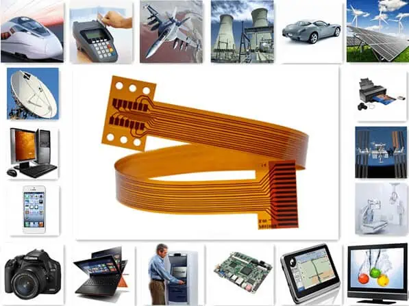
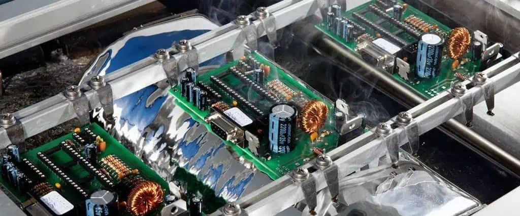
Joining metal parts is critical in manufacturing across industries including electronics, automotive, aerospace, machinery and more. Soldering is the most common electrical interconnection method used to attach electronic components to printed circuit boards (PCBs). However, emerging direct solid-state joining techniques like cold welding and pseudo-soldering are gaining attention as lead-free solder alternatives.

This article provides an in-depth comparison between cold welding and pseudo-soldering processes encompassing the bonding mechanisms, joint microstructures, applicability for electronics assembly, processing considerations, joint strength and reliability. By understanding the capabilities and limitations of both methods, engineers can select the right approach for manufacturing robust metal-to-metal interconnects.

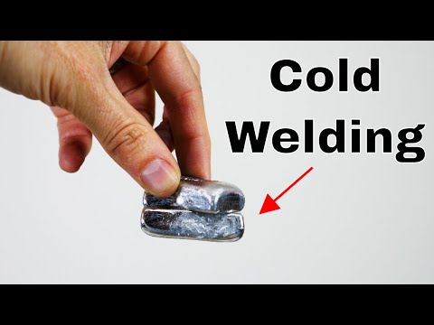
What is Cold Welding?

Cold welding refers to solid-state joining of metals well below their melting points by applying high pressures to create intimate contact between atomically clean surfaces. This allows interatomic bonding across the interface without fusion of the base metals or use of filler alloys.

The bond initially forms due to Van der Waals forces between surface atoms. Further plastic deformation under pressure breaks up surface films and contaminants enabling actual metallic bonds between the virgin parent metal lattices.

What is Pseudo-Soldering?

Pseudo-soldering produces solder-like intermetallic joints through solid-state interdiffusion between metal foils and substrates at temperatures below the bulk metal melting points. Specially formulated multi-layer composite foils are placed between parts and heated under pressure. Interdiffusion between the intermediate reactive layers and the substrates creates intermetallic phases that join the parts.

The intermetallics grow similar to transient liquid phase bonding in soldering, but without becoming molten. Hence the name pseudo-soldering. The intermetallic joint resembles solder in appearance and meets process requirements for electronics assembly.

Bonding Mechanisms Comparison

ParameterCold WeldingPseudo-Soldering
Bond FormationMetallic bonds between cleaned metal surface atomsInterdiffusion creates intermetallic phases
Base Metal StateRemains solidRemains solid
Intermediate PhasesNoneIntermetallic transient liquid phase
Pressure NeededHigh (25-100 MPa)Lower (3-10 MPa)
Bonding TemperatureAmbient to 300ยฐC180ยฐC to 350ยฐC
Surface Finish DependencyHighly dependentDepends on interlayer
Reactivity with MetalsLowHigh due to interlayers

Joint Microstructure Comparison

Cold Welded Interface

The interface preserves parent metal microstructures with minimal heat affected zones. Direct metallic bonds reform across the interface. Some trapped oxides or voids may remain.

Pseudo-soldered Interface

Intermetallic compounds form across the interface analogous to soldered joints. The intermetallic thickness depends on thermal exposure. Minimal heat affected zones are present.

Electronics Assembly Comparison

ParameterCold WeldingPseudo-Soldering
Process TemperaturesUp to 300ยฐC180ยฐC to 350ยฐC
Pressure NeededVery highModerate
Tooling ComplexityHighLow to moderate
Throughput SpeedSlowModerate
Surface SensitivityHighLow
Component MetallizationsLimited material compatibilityWide material compatibility
Defect SensitivityLowHigher voids, bridges
Design AdaptabilityRequires major redesignDrop-in solder alternative
Equipment InvestmentVery highModerate modifications

Bond Strength Comparison

Well bonded joints exhibit parent metal fracture strengths proving the interface is stronger than the base metals. Joint strengths over 200 MPa are easily achieved for many material combinations with both cold welding and pseudo-soldering.

However, actual bond strengths depend significantly on surface cleanliness, flatness, pressure consistency, metallurgical compatibility, and process parameter control. Defects like trapped oxides, voids, and poor interdiffusion lower bonding strength and reliability.

Reliability Considerations

Cold Welded Joints

  • Prone to stress corrosion cracking along trapped oxide zones
  • Subject to fatigue failure under thermal cycling due to high elastic modulus mismatch across interface
  • Hermetic seals can be achieved

Pseudo-soldered Joints

  • Intermetallic compounds may suffer thermal fatigue and brittle failure
  • Interdiffusion quality affects electromigration resistance
  • Lower hermeticity due to defects
  • Comparable to solder joint reliability with intermetallics

Cost Analysis

What is Solder Beading?

Cold Welding Equipment

Requires high tonnage presses, precision tooling, surface preparation equipment, and automation. Overall capital equipment cost is very high.

Pseudo-soldering Equipment

Moderate modifications to existing soldering infrastructure like ovens, conveyors and simple tooling. Capital equipment cost is low to moderate.

Consumables

Cold welding has no recurring consumable costs. Pseudo-soldering requires proprietary foil stacks resulting in moderate consumable costs.

Pros and Cons Summary

Cold Welding

Pros

  • Strong direct metallic bonds
  • No intermetallics or heat affected zones
  • Hermetic capability
  • No fluxes or volatiles

Cons

  • Very high pressure needed
  • Limited material compatibility
  • High surface cleanliness needed
  • Slow process speed and throughput
  • High equipment and tooling costs

Pseudo-soldering

Pros

  • Solder-like bonds with wide material compatibility
  • Lower pressures sufficient
  • Adaptable process requiring minimal changes
  • Fast process analogous to soldering
  • Lower equipment costs

Cons

  • Intermetallic reliability concerns
  • Potential for voids and bridges
  • Recurring consumable costs
  • Hermeticity challenges
  • Thermal fatigue susceptibility

Conclusion

Cold welding can produce exceptionally strong metallic joints but requires significant process development and equipment investments. Pseudo-soldering offers more accessible solder-alternative capabilities but shares common concerns with intermetallic solder bonds. Engineers can utilize this comparative knowledge of both technologies to select the optimal solid-state bonding process for their manufacturing needs after factoring in joint performance requirements, production volumes and equipment costs trade-offs.

Frequently Asked Questions (FQA)

Q1: What metals can be successfully joined through cold welding?

A1: Most ductile metals like gold, silver, aluminum, copper, mild steels can cold weld readily while brittle metals like cast iron and titanium are not suitable. Hardness mismatch and metallurgical incompatibility can also limit bondability between certain material combinations.

Q2: What are some common applications of cold welding?

A2: Cold pressure welding is used to make welded metal bellows, hermetic seals, electrical contacts, metal assemblies in aerospace, automotive and medical products. Micro-scale cold welding is used in MEMS device fabrication.

Q3: How does the surface roughness of the metals to be joined impact the pseudo-soldering process?

A3: Minimal impact since the interlayers deform and diffuse into the base metals to form intermetallic bonds. However, highly polished surfaces allow better interfacial contact enabling faster interdiffusion. Excessively rough surfaces may trap more voids.

Q4: What types of intermetallics form in a typical pseudo-soldered joint between copper substrates?

A4: Intermetallics like Cu3Sn and Cu6Sn5 form during solid state interdiffusion between copper and tin across the joint interface, similar to conventional copper-tin solder joints. The final intermetallic distribution depends on bonding time and temperature.

Q5: What are some methods used to clean metal surfaces prior to cold welding?

A5: Chemical etching, electrochemical polishing, sputter cleaning, ion beam cleaning and precision machining are typically employed. The goal is to remove all surface oxides, films and organic residues to enable direct metal-to-metal bonding.

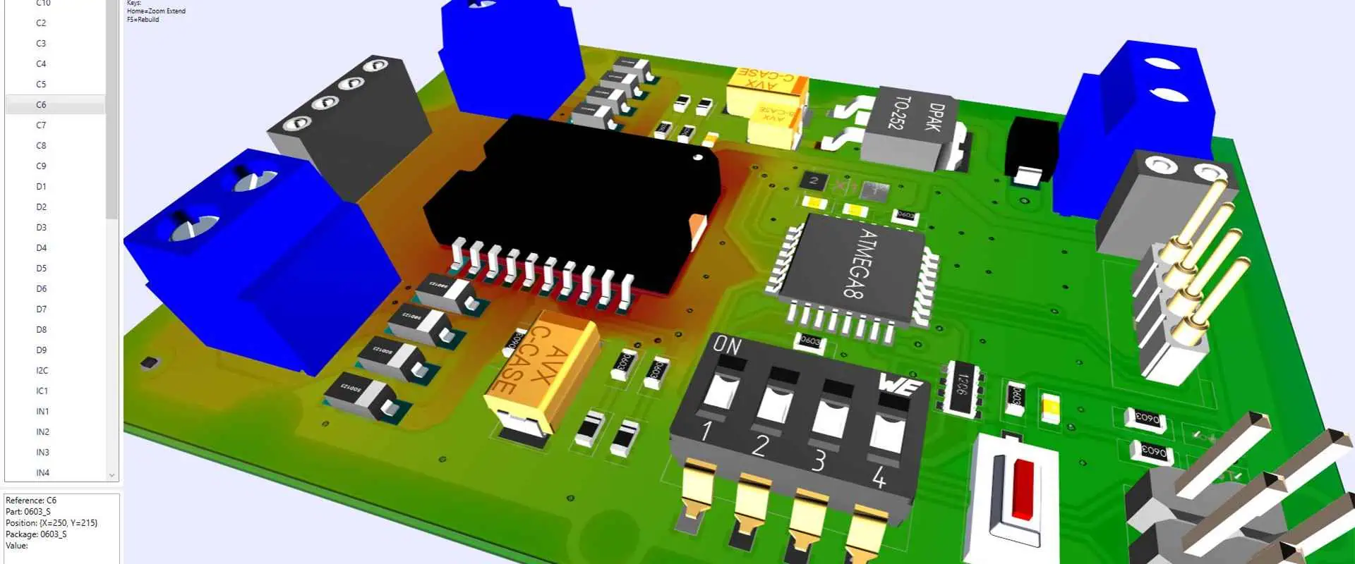
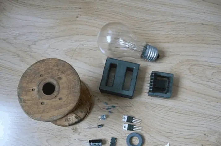
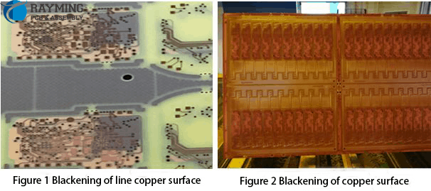
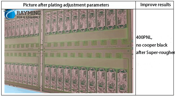
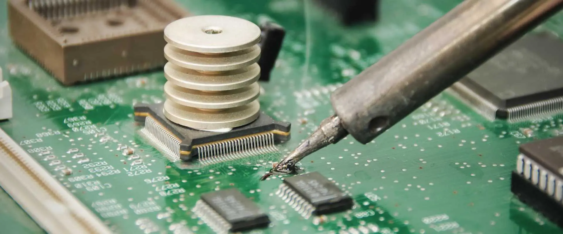
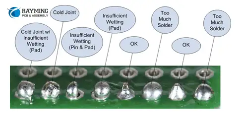
Definition of PCBA cold welding

When the minimum required wetting temperature is not reached between the electronic component and the PCB during soldering; or although the local wetting occurs, the phenomenon caused by incomplete metallurgical reaction can be defined as cold soldering. Popularly speaking, it is caused by low temperature.

YouTube video
SMT PCBA

The difference between PCBA cold welding and pseudo soldering

1.The color is different

Cold soldering is generally a color difference,the color will be black, and even serious can see tin particles.

2.The mechanism of formation is different

The pseudo soldering is caused by the oxidation, vulcanization or contamination of the surface of the soldered metal and becomes non-weldable, while the cold soldering is caused by insufficient heat supplied by the PCBA board during soldering.

3.There are differences in connection strength

In the case of soldering, the solder and the metal surface of the substrate are separated from each other by an oxide film. After bonding, the adhesion of the solder is poor, and the bonding effect is weak. The IMC layer formed on the interface of the cold solder joint is very Thin and incomplete development, and the interface of solder joints with severe cold welding is often accompanied by penetrating cracks, and there is no strength at all.

4.Metallographic structure is different

The microstructure of the metallurgical structure after the virtual welding is relatively fine; the microstructure of the metallographic structure after cold welding is not uniform.

Both PCBA and cold soldering directly affect the reliability of prototype PCB Assembly soldering. It is necessary to detect and prevent it in time to effectively reduce the repair rate of PCBA board.

High Thermal Conductivity PCB Material Will Solve The Heat Dissipation Problem

fr4 thermal conductivity

With the development of integration technology and microelectronic packaging technology, the total power density of electronic components is increasing, while the physical dimensions of electronic components and electronic devices are gradually becoming smaller and miniaturized, and the generated heat is rapidly accumulated, leading to integration. The heat flux density around the device is also increasing, so the high temperature environment will definitely affect the performance of electronic components and equipment, which requires a more efficient thermal control scheme. Therefore, the heat dissipation problem of electronic components has evolved into a major focus of current electronic components and electronic device manufacturing.

YouTube video

In response to this situation, engineers have come up with some thermal management strategies: for example, by increasing the thermal conductivity of the PCB (high TC) to improve heat dissipation; focusing on allowing materials and devices to withstand higher operating temperatures (high Thermal Decomposition Temperature) Strategy; need to understand the operating environment and the thermal adaptation of the material to the degree of thermal cycling (low CTE). Another strategy is to use more efficient, lower power or lower loss materials to reduce heat generation.

thick copper pcb

There are three general heat dissipation methods: heat conduction, convection, and radiation heat transfer. Therefore, the commonly used thermal management methods are as follows: whenย designing the circuit board, deliberately increase the thickness of the heat-dissipating copper foil or use a large-area power supply, ground copper foil; use more heat-conducting holes; use metal heat dissipation, including heat sink, local Inlaid copper block. Or in the assembly, add a heat sink to the high-power device, the whole machine is added with a fan; either use thermal conductive adhesive, thermal grease or other thermal conductive material; or use heat pipe cooling, steam cavity radiator, high efficiency radiator.

At present, a new thermal solution has emerged on the market: it is advocated to use high Thermal Decomposition Temperature (TD) and high thermal conductivity (TC) plates for circuit board design. For example, Rayming currently represents ROGERSโ€™s 92ML series laminates. As a global leader in high-frequency circuit materials, Rogersโ€™ high thermal conductivity PCB material 92 ML series has several excellent features, the most notable of which is that the thermal conductivity of rogers 92ML is 4 to 8 times that of standard FR-4 (epoxy).

special pcb

The characteristics of the high thermal conductivity PCB material rogers 92 ML are as follows:

  • Thermal conductivity (Z-axis) is 2W/M.K (ASTM E1461)
  • Glass transition temperature Tg: 160 ยฐC
  • Thermal Decomposition TemperatureTd: 400 ยฐ C (5%)
  • Z-axis thermal expansion coefficient (50-260 ยฐ C): 1.8%
  • UL maximum operating temperature: 150 ยฐ C
  • The same medium thickness withstand voltage is higher, the stability is good, suitable for high power and high pressure design
  • Halogen free
High-Frequency-PCB

Then, compared with the general thermal management plan, where is the Raymingย rogers pcbย 92ML material solution winning?

In standard industrial test methods and models, it is assumed that the material is isotropic and only passes through the thermal conductivity of the plane; planar heat dissipation is usually used to reduce the hot spot temperature and increase the heat transfer throughout the region. The Rayming 92ML solution not only reduces the junction temperature of the device, but also increases the power output by about 15% or higher. Compared to the conventional FR-4, the 92ML can be further reduced by 30 ยฐ C to 35 ยฐ C (depending on the specific design).

It can also reduce the hot spot peak temperature by increasing the Z-axis heat transfer and increasing the thermal diffusion of the X and Y axes. With a 1โ„4 brick DC-DC converter that does not exceed the recommended temperature of the device, it also has a higher power output, and an increase in heat transfer also increases power capacity. Moreover, the rogers 92ML solution has a very strict design for flatness and improves the flatness of the PCB. Its lower Z expansion factor also increases PTH reliability. The 92 ML series is available: prepreg, copper clad, metal substrate (SC92ยฎ); and the test sample has passed the Interconnect Stress Test (IST).

What is Differences Between Fr4 Glassfiber and Aluminum substrate for PCB?

aluminum substrate pcb

Introduction

Printed circuit boards (PCBs) are essential components of modern electronics. A PCB provides mechanical support and electrically connects different components using copper traces etched from copper sheets laminated onto a non-conductive substrate material. The substrate material plays a vital role in determining the performance and characteristics of the PCB. The two most common substrate materials used today are FR4 glass epoxy and aluminum.

FR4 glass epoxy is the ubiquitous substrate material used in the majority of PCBs. However, for certain demanding applications where high performance and thermal management are critical, aluminum substrates are being increasingly adopted.

This article provides a detailed comparison between FR4 and aluminum PCB substrates across various parameters like electrical performance, thermal conductivity, mechanical strength, ease of manufacturing, and cost. Understanding the pros and cons of both materials will help design engineers select the right substrate for their specific application requirements.

Electrical Performance

aluminum pcb Vs Fr4 PCB

Dielectric Constant

The dielectric constant of the substrate influences impedance control, signal integrity, and crosstalk on the PCB. The dielectric constant of FR4 is typically between 4.2 to 4.6 over the signal frequency range. In comparison, aluminum substrates have a lower dielectric constant of around 3.7.

The lower dielectric constant of aluminum allows tighter trace spacing and routing on outer layers without compromising signal integrity. This makes aluminum suitable for densely populated high-speed digital boards requiring tight impedance control.

Loss Tangent

The loss tangent indicates the inherent signal loss in the substrate material. FR4 has a loss tangent ranging from 0.01 to 0.025. In comparison, aluminum has an extremely low loss tangent of 0.001.

The lower loss tangent translates to lower signal loss and intersymbol interference. High-speed signals experience less distortion over aluminum substrates compared to FR4. This allows aluminum substrates to support higher signal frequencies and data rates.

Insulation Resistance

Insulation resistance indicates how effectively the substrate can insulate between conductors or layers carrying different signals. FR4 typically has an insulation resistance above 1000 Mฮฉ. Aluminum substrates have a much lower insulation resistance of around 10-25 Mฮฉ.

While the insulation resistance of FR4 is adequate for most applications, the lower insulation resistance of aluminum substrates makes them unsuitable for high-voltage boards.

Breakdown Voltage

Breakdown voltage is the maximum voltage that can be applied across the substrate before electrical breakdown occurs. FR4 has a breakdown voltage of around 12 kV/mm. Aluminum substrates have a comparatively lower breakdown voltage of 1.5 kV/mm.

The high breakdown voltage allows FR4 boards to operate safely at higher voltages. Aluminum substrates are not recommended where high potentials may be present between conductors or layers.

Summary of Electrical Performance

Electrical PropertyFR4Aluminum
Dielectric Constant4.2 – 4.63.7
Loss Tangent0.01 – 0.0250.001
Insulation Resistance>1000 Mฮฉ10-25 Mฮฉ
Breakdown Voltage12 kV/mm1.5 kV/mm

Thermal Performance

Thermal Conductivity

The thermal conductivity of the substrate determines how efficiently heat can be conducted across the PCB. FR4 has a poor thermal conductivity around 0.25 W/mK. In comparison, aluminum has a very high thermal conductivity of 237 W/mK.

The high thermal conductivity of aluminum allows it to rapidly conduct heat away from hot components. This makes aluminum substrates ideal for thermal management in high-power boards. FR4 does not conduct heat well, leading to localized heating and reliability issues.

Coefficient of Thermal Expansion (CTE)

The CTE indicates how much the material dimensions change with temperature. FR4 has a CTE of around 14-16 ppm/ยฐC. Aluminum has a CTE of 23 ppm/ยฐC.

The CTE mismatch between FR4, copper traces, and components leads to thermal stresses during heating and cooling cycles. Aluminum’s CTE is closer to copper, reducing thermal stresses on interconnects.

Thermal Cycles Withstood

Repeated thermal cycling can lead to failures like solder cracks and delamination due to material expansion and contractions. FR4 can typically withstand around 150 cycles from 0ยฐC to 100ยฐC. Aluminum substrates can endure over 2000 such cycles without failures.

Aluminum’s superior thermal cycling capability makes it suitable for applications with frequent thermal load fluctuations like aerospace and automotive.

Maximum Operating Temperature

The maximum temperature a substrate can reliably operate at depends on the glass transition temperature for organic materials like FR4 and the melting point for metals like aluminum. FR4 has a glass transition temperature of around 130ยฐC. Aluminum has a higher melting point of 660ยฐC.

The higher maximum operating temperature rating allows aluminum substrates to function in high-temperature environments beyond the capability of FR4 boards.

Summary of Thermal Performance

Thermal PropertyFR4Aluminum
Thermal Conductivity0.25 W/mK237 W/mK
CTE14-16 ppm/ยฐC23 ppm/ยฐC
Thermal Cycles Withstood150 (0ยฐC to 100ยฐC)2000+ (0ยฐC to 100ยฐC)
Max Operating Temperature130ยฐC660ยฐC

Mechanical Performance

FR4-PCB-Material

Flexural Strength

Flexural or bend strength indicates the ability of the substrate to withstand bending forces without damage. FR4 has a flexural strength of around 275-380 MPa. Aluminum has a higher flexural strength of 110-350 MPa depending on the alloy.

The higher flexural strength provides more mechanical robustness to aluminum substrates compared to FR4.

Tensile Strength

Tensile strength indicates the ability to withstand tensile loads before fracturing. FR4 has relatively low tensile strength of 70-80 MPa. Aluminum has a tensile strength of 90-190 MPa depending on the alloy.

Aluminum substrates can endure higher pulling or tension forces compared to FR4 substrates.

Hardness

Hardness indicates the resistance of the material to indentation, scratching, and abrasion. On the Rockwell scale, FR4 has a hardness of 100-110. Aluminum has a lower hardness of 25-50 depending on the alloy.

The higher hardness provides FR4 substrates better resistance against physical damage like scratches compared to softer aluminum.

Density

Density is the mass per unit volume of the substrate material. FR4 has a density of 1900-2000 kg/m<sup>3</sup>. Aluminum has a lower density of 2700 kg/m<sup>3</sup>.

The lower density of FR4 provides a weight advantage in weight-sensitive aerospace and portable applications.

Summary of Mechanical Performance

Mechanical PropertyFR4Aluminum
Flexural Strength275-380 MPa110-350 MPa
Tensile Strength70-80 MPa90-190 MPa
Hardness100-110 (Rockwell)25-50 (Rockwell)
Density1900-2000 kg/m<sup>3</sup>2700 kg/m<sup>3</sup>

Manufacturability

Layer Count

Modern PCBs utilize multi-layer designs to accommodate complex circuity and component density requirements. FR4 boards are available in high layer counts of over 30 layers from mainstream manufacturers. In comparison, aluminum boards are typically restricted to 2 or 4 layers.

For simpler boards, aluminum substrates can provide adequate layer counts. But for complex multilayer applications, FR4 provides far greater flexibility.

Via and Hole Fabrication

Vias and through-holes on PCBs allow interconnection between layers and component terminations. The standard process of drilling and plating holes is easily done on FR4 boards. But drilling smooth holes in aluminum is difficult due to the tendency of aluminum to smear around drill bits.

Mechanical punching and microvia laser drilling techniques allow holes to be formed in aluminum, but at higher cost. This restricts the minumum via size achievable on aluminum boards.

Component Assembly

Soldering is the predominant method of attaching components onto PCBs. The glass transition temperature of FR4 allows it to withstand soldering temperatures with minimal damage. Aluminum can dissolve into molten solder or get oxidized at elevated temperatures, requiring specialized soldering processes.

Aluminum boards may need higher temperature solders and fluxes as well as protective coatings in pad areas. This complicates component assembly compared to FR4 boards.

Material Availability

FR4 laminates are manufactured globally in large volumes and are readily available at low cost. In contrast, aluminum PCB substrates require specialized fabrication and have lower availability. Lead times over 8 weeks are common for aluminum boards.

For prototyping and production ramp-up, FR4 offers a time-to-market advantage over aluminum substrates.

Summary of Manufacturability Comparison

Manufacturing ParameterFR4Aluminum
Max Layer Count>30 layers2-4 layers
Via/Hole FabricationStandard drilling/platingChallenging
Component AssemblyStandard solderingSpecialized processes
Material AvailabilityReadily availableLower, longer lead times

Environmental Performance

Operating Temperature Range

As discussed earlier, the maximum operating temperature of FR4 is around 130ยฐC. Aluminum substrates can operate to over 300ยฐC.

For applications with temperature requirements beyond 130ยฐC, aluminum provides the only option. FR4 substrates will be unsuitable beyond their glass transition point.

Resistance to Solvents

Organic substrates like FR4 can be attacked by strong solvents like acetone leading to swelling and mechanical damage. Aluminum exhibits excellent chemical resistance and is unaffected by solvents.

In applications where solvent resistance is critical like military avionics, aluminum provides a durable substrate resistant to chemicals.

Flame Retardancy

FR4 is naturally flammable due to its resin system. Flame retardants are incorporated to provide V-0 and V-1 flame ratings as per UL 94 standards. In contrast, aluminum is intrinsically non-flammable and does not require flame retardant additives.

For safety-critical applications like automotive, aluminum substrates eliminate the risk of flammability and smoke/toxic gas generation during fires.

Outgassing and Vacuum Compatibility

In vacuum environments, organic substrates like FR4 outgas moisture and other volatiles that can condense on sensitive surfaces. Aluminum has negligible outgassing and is well-suited for space and vacuum applications.

Additionally, FR4 laminates absorb atmospheric moisture affecting electrical performance. Aluminum substrates have lower moisture absorption issues.

Summary of Environmental Performance

Environmental AspectFR4Aluminum
Max Operating Temperature130ยฐC>300ยฐC
Solvent ResistancePoorExcellent
FlammabilityV-0, V-1 ratingsNon-flammable
Outgassing/Vacuum CompatibilityHigh outgassingNegligible outgassing
Moisture AbsorptionHighLow

Cost Considerations

Aluminum PCB substrates are significantly more expensive than conventional FR4 laminates. Raw material costs of aluminum are higher. Additional fabrication steps like thermal bonding of insulation layers and specialized hole-making techniques also add cost.

Complex multilayer aluminum boards can cost anywhere from 5-10 times more than an equivalent FR4 board. However, for demanding applications where performance merits the cost, aluminum may still provide the optimal value proposition.

Summary of FR4 vs Aluminum Substrates

ParameterFR4Aluminum
Electrical PerformanceModerateExcellent signal integrity
Thermal PerformancePoorExcellent thermal conductivity
Mechanical PerformanceModerate strength and hardnessHigher strength
ManufacturabilityExcellent, well-establishedChallenging
Environmental PerformanceModerate thermal and chemical resistanceExcellent high-temp and chemical resistance
CostLow5X to 10X of FR4

When to use FR4?

  • Cost-sensitive applications
  • Consumer electronics with moderate performance requirements
  • Multi-layer complex boards >8 layers
  • Applications operating below 130ยฐC

When to use Aluminum?

  • High-frequency RF/analog circuits requiring tight impedance control
  • High-power boards requiring heat dissipation (>3 kW/m2)
  • Rugged boards requiring high mechanical strength
  • Boards requiring resistance to high temperatures, chemicals, fire
  • Applications with weight constraints like aerospace and portable devices

Conclusion

FR4 continues to be the dominant PCB substrate with its balanced electrical performance, fabrication ease and low cost. Aluminum substrates provide superior thermal management, signal integrity, and environmental resistance but at significantly higher cost.

Engineers should weigh these trade-offs for their particular application requirements while selecting between the two. Hybrid boards combining aluminum base layers for thermal spreading and FR4 outer layers are also an option. The continued innovation in board materials will provide ever more options to designers to optimize the PCB substrate.

Frequently Asked Questions (FQA)

Q1: How are aluminum PCBs insulated if aluminum itself conducts electricity?

A1: Aluminum is sandwiched between insulating dielectric layers to prevent electrical conduction through the aluminum core. These dielectric layers typically use thermally conductive ceramics like aluminum oxide or aluminum nitride that are bonded to the aluminum under high pressure and temperature. This creates a well-insulated aluminum substrate.

Q2: Can components be soldered directly onto aluminum PCBs?

A2: Directly soldering component leads onto aluminum can cause metallurgical issues like solder voids, dissolution of aluminum into solder, and oxidation. To avoid this, aluminum boards usually have copper pads and lands on the outer layers where components are placed and soldered. Additionally, protective coatings like nickel or gold may be applied selectively over aluminum areas needing soldering.

Q3: Are aluminum PCBs prone to corrosion?

A3: Bare aluminum is prone to surface oxidation and corrosion when exposed to moisture. However, aluminum PCB substrates are coated with protective lacquers, anodization layers or conformal coatings to prevent corrosion. This provides excellent protection against harsh operating environments.

Q4: Can aluminum PCBs be made with as many layers as FR4 PCBs?

A4: Manufacturing technology currently limits aluminum-based boards to 2 or 4 layers in most cases. The difficulties in insulating layer bonding and drilling/plating via holes makes building complex multi-layer aluminum boards very challenging. FR4 based boards can reach over 30 layers using established processes.

Q5: Does weight saving justify the use of aluminum instead of FR4?

A5: In very weight-sensitive applications like aerospace, the lower density and weight of aluminum can provide tangible benefits. Up to 15% weight reduction is possible with aluminum versus FR4 boards of similar size. However, this advantage diminishes if aluminum is only used selectively in the core layers, with FR4 used on outer layers. The weight saving should be weighed against the higher cost.

What Is The FPC Board Manufacturing Process?

one layer flex pcb board

Introduction

Flexible printed circuit boards (FPCs) enable reliable interconnects and circuits in applications where rigid boards are impractical. Producing high quality FPCs requires specialized fabrication processes tailored for flexible substrates.

This article provides an in-depth look at the end-to-end FPC manufacturing process. Weโ€™ll explore the step-by-step sequence from material preparation through final fabrication. Understanding the considerations at each stage allows designers to optimize designs for manufacturability and achieve consistent results.

By the end, the full progression for transforming raw materials into complete FPC assemblies will be clear.

FPC Board Materials

Creating the flex board begins with selecting suitable substrate and coverlay materials:

Base Dielectric

  • Polyimide films like Kapton are most common
  • Other options include PET, PEN, PI composites

Bonding Adhesives

  • Acrylic or epoxy adhesives
  • Thermally activated bonding films

Coverlay

  • Liquid photoimageable solder mask (LPI)
  • Adhesive coated polyimide laminates

Stiffeners

  • Polyimide, FR4, aluminum inserts

Materials are certified to IPC specs ensuring consistent quality and performance.

Copper Clad Laminates

Rolls of copper clad flex laminate formed through adhesive bonding:

  • Available in single or double sided
  • Standard 1/2 to 2 oz copper foils
  • Available on quick-turn rolls or panels
  • Cut to size for specific designs

Large volume cost savings result from maximizing material utilization.

Inner Layer Preparation

Multilayer FPCs require individually imaging inner layers:

  • Copper patterning using lithography
  • Etch away unwanted copper
  • Strip photoresist masks
  • Visually inspect layer quality
  • Electrical testing checks shorts and opens

Completed inner layers are interleaved during layup and lamination.

Layup and Lamination

FPC material layers are stacked and bonded together:

  • Cut materials to size for each design
  • Clean all layers to remove debris
  • Precisely align films and foils
  • Load into thermal presses
  • Apply heat and pressure cycle
  • Cool under controlled pressure

Result is a solid laminate with all layers fused into a monolithic board.

Drilling

Holes drilled through the laminated stack:

  • Tooling holes for alignment
  • Through vias for interconnection
  • Depth controlled vias in multilayer boards
  • Precise process prevents barreling or tearing
  • Deburring cleans up hole walls

Hole walls prepared for subsequent plating process.

Hole Metallization

Coat drilled holes with conductive material using electroless and electrolytic plating processes:

  • Electroless copper builds initial seed layer
  • Electrolytic copper plates up conductive hole barrels
  • Copper thickness from 0.5 to >25 microns
  • Optional tin or gold finish over copper

This creates electrical connections between layers through drilled vias.

Patterning

With substrates fully prepared, photolithographic imaging defines circuit conductors:

  • Apply photoresist layer onto copper
  • Expose with UV through patterning artwork
  • Develop to selectively remove resist
  • Etch exposed copper regions
  • Strip remaining resist after etch
  • Repeat for double sided circuits

Result is the complete desired conductor pattern on the flex board.

Solder Mask

Solder mask is applied to prevent solder bridging and protect traces:

  • Liquid photoimageable mask (LPI) typically used
  • Screens away mask from desired exposed pads
  • Cures mask into tough permanent layer
  • Optional selective openings for test points

Provides electrical and environmental insulation to the circuitry.

Silk Screening

Printed silkscreen legends help identify components and connectors:

  • Ink applied through patterned screens
  • Denotes polarity, part numbers, text
  • Highly durable epoxy ink resists wear
  • White legend on black mask is common
  • Also used for board outlines/scoring

Silkscreen guides assembly and identifies the board.

Stiffener Attachment

FR4 Stiffener

Optional stiffeners added to reinforce boards:

  • Cut metal or laminate layers to size
  • Bond in place with adhesive films
  • Improves connector durability
  • Located only in required high stress areas

Stiffeners prevent flexing damage but increase cost.

Electrical Testing

Each board validated electrically after completion:

  • Tests check for short and open circuits
  • Validates design connectivity
  • Detects any fabrication defects
  • Testing may also include loaded capacitance and impedance measurements

Confirms properly functioning boards before shipment and assembly.

Final Processing

FPCs undergo final steps before shipment:

  • Route scores for break-apart boards
  • V-score flexing joints
  • Edge bead removal along routed edges
  • Cleaning removes residues
  • Package boards to avoid damage during shipment

Resulting finished FPCs are ready for customer assembly.

Conclusion

While requiring tight process control, the sequence of FPC fabrication steps enables reliable flexible printed circuits. Understanding the progression from raw materials through finished boards allows designers to optimize designs for manufacturability. The specialized fabrication processes produce high performance FPCs able to withstand dynamic mechanical environments.

Frequently Asked Questions

Q: What are typical FPC substrate and copper thicknesses?

A: Polyimide dielectric films commonly range from 1 to 5 mils. Copper foil is usually 0.5 to 2 oz (18 to 70 microns).

Q: How many FPC circuit layers can be fabricated?

A: Practical limits are typically around 12 layers. More than 20 requires special processes with limited suppliers.

Q: What minimum trace/space is achievable on FPCs?

A: 3/3 mil lines/spaces are typical on outer layers. 5/5 mil tolerances for buried traces. Even smaller features possible with advanced equipment.

Q: What types of connectors mount to FPC boards?

A: Common connectors are pressure-contact ZIF types or flex-tail soldered terminals into plated through holes.

Q: What are recommended design for assembly guidelines for FPCs?

A: Allow tolerance for misalignment, provide strain relief, keep components small and low-mass, and minimize mechanical stress points.

How Do You Design a Power Supply?

power pcb

Introduction

A power supply is a crucial component that converts power from a source to the regulated voltages required by electronic circuits and systems. The proliferation of electronic devices has led to power supplies being ubiquitous, ranging from chargers for mobile phones to high capacity supplies in data centers. Designing a proper power supply requires expertise in multiple engineering domains encompassing power electronics, analog design, control theory, and thermal management.

This article provides a step-by-step guide on designing a power supply covering aspects like topology selection, power stage design, feedback and control, safety standards compliance, thermal design, and electromagnetic compatibility. By following the structured design methodology, electrical engineers can develop reliable and efficient power supplies tailored to their application needs.

Functional Requirements

Switching Power Supply Design

Defining the right specifications and functional requirements is the critical first step that sets the overall direction for the power supply design.

Input Voltage Range

The expected input voltage range should be specified, including minimum, nominal, and maximum voltages. Common input ranges are 5V, 12V, 24V, or 48VDC derived from rectified mains AC or batteries. Wider input ranges require designs that can maintain regulation over the span.

Output Voltages and Currents

The desired output voltages and load currents should be specified. For multiple outputs, cross-load dependencies and sequencing needs must also be considered. Safe margins above nominal loads should be included for fault conditions. Prioritizing critical outputs helps allocate design resources effectively.

Efficiency Targets

Required full load and partial load efficiencies at nominal voltages determine components selection and loss budgeting. Light load efficiency is also critical for new energy-efficiency standards.

Power Density Targets

The desired power density (watts/cubic inches) influences how compactly the design must be packaged. It requires trade-offs with efficiency and thermal performance.

Safety and Emissions Compliance

Regulatory standards like medical and IT equipment safety, conducted emissions, and radiated emissions compliance must be considered.

Reliability Requirements

Requirements like MTBF, expected service life, and environmental survival ranges help guide design choices for component deratings and redundancies.

Control Characteristics

Needs like remote control, sequencing, telemetry, and margining control influence digital control and communication features.

Topology Selection

The choice of power conversion topology sets the foundation for meeting the design goals. Different topologies have inherent advantages and limitations.

Linear Regulator

A linear regulator maintains output voltage by dropping excess input voltage across a series pass element. The advantages are simplicity, low noise, and fast response. But poor efficiency at lower output voltages makes them unsuitable for high power applications.

Switching Regulator

Switching converters use semiconductor switches to transfer chunks of energy to the output in a controlled pulsed manner. Switching loss is lower than a linear regulator, allowing high efficiency conversion even for large voltage drops. However, switching noise requires careful filtering.

Various sub-classes of switching regulators offer further topological choices:

  • Buck Converters: Used for step-down conversion from higher input to lower output voltage.
  • Boost Converters: Used for step-up conversion from lower input to higher output voltage.
  • Buck-Boost Converters: Allows both step-down and step-up conversion flexibly.
  • Isolated Topologies: Flyback, forward, push-pull, and full-bridge converters use transformers for isolation and multiple outputs.

Selection criteria include required conversion ratio, complexity, component stresses, efficiency, and isolation needs.

Resonant and Soft-Switching Topologies

Resonant converters and quasi-resonant soft-switching schemes reduce switching losses allowing very high efficiency conversion. However, the added complexity may not justify gains for lower power applications.

Power Stage Design

pcb-power-supply

The power stage handles the actual power conversion between input and output. It consists of elements like switches, diodes, inductors, transformers, and capacitors.

Semiconductor Switch Selection

MOSFETs and IGBTs are suitable semiconductor switch choices for power supplies below 500W. High current capability MOSFETs allow simpler synchronous rectifier buck designs. Above 500W, IGBTs tend to be more robust. Availability of integrated power modules with paralleled devices simplifies high current designs.

Passive Components

  • Inductors: Value selection involves tradeoffs between ripple, response time, and component size. Core materials and shapes like toroids or pot cores optimize efficiency.
  • Transformers: Core geometry, materials, gap design, winding techniques, and layered or interleaved windings affect performance.
  • Capacitors: A mix of electrolytic and multilayer ceramic capacitors provides bulk capacitance and high frequency bypassing.

Snubbers and Clamps

Snubbers like RC networks suppress voltage spikes across switches during switching transitions. Clamps help limit overvoltage events.

Layout and Parasitics

Careful component placement and routing minimizes the length of high current paths to reduce parasitic inductance and resistance. Separating noisy switching nodes from sensitive analog areas is necessary.

Feedback and Control

To maintain stable regulated output voltages, feedback control forms a closed loop system adjusting PWM switching patterns based on output voltage deviations from the reference.

Voltage Dividers

Properly designed resistive divider networks scale output voltages to levels acceptable for the feedback IC. Filtering may be required for noise reduction.

Feedback IC

Specialist ICs provide operational amplifier, pulse width modulation (PWM), compensation circuits and protection features needed for robust control and regulation of switching converters.

Compensation Network

This provides the corrective feedback and stability for the control loop. The network sets gain crossover and phase margin by shaping the IC loop gain to target stable response with adequate noise immunity.

Digital Control

Incorporates monitoring, diagnostics, communication, and adaptive tuning functions via a microcontroller. This allows sophisticated control algorithms and remote user interfaces.

Protection Features

Protection safeguards the power supply and connected load during abnormal conditions. Common protections include:

  • Overvoltage protection – Shuts down supply if output exceeds preset safe threshold.
  • Undervoltage protection – Shuts down supply if output sags excessively under minimum level.
  • Overcurrent protection – Shuts down supply if load current exceeds set limit indicating a short circuit.
  • Over temperature protection – Shuts down supply if internal temperatures rise beyond safe operating limit.
  • Input under/over voltage lockout – Disables output if input is outside operating range.
  • Redundancy – Secondary backup units takeover upon failure detection
  • Surge and transient protection – MOVs, RC snubbers absorb incoming surges on input.

Thermal Design

Generating substantial heat is an inherent consequence of power conversion. Effective thermal management is vital for reliable operation and safety.

Power Dissipation Analysis

The distribution of losses in switches, magnetics, and other components determines cooling requirements. Analytically derived and validated through simulations.

Heatsink Design

Heatsinks provide convective cooling matched to the power dissipation profile. Fin geometry, airflow passage design, heat pipe augmentation, and interface materials influence heatsink performance.

Airflow and Ventilation

Fans and airflow ducting maintain sufficient directed airflow through heatsinks and the housing. Intake and exhaust vents are designed to utilize natural convection also.

Thermal Interface Materials (TIMs)

TIMs like thermal pads, greases, or phase-change compounds improve heat conduction from components to heatsinks.

EMI/EMC Design

High Power PCB Design

Switching power supplies generate significant high-frequency noise requiring careful mitigation to meet EMI limits and prevent conducted/radiated interference with other devices.

Input Filtering

Pi-filters and ferrite beads supress current-driven differential mode noise propagating from the AC input to the power stage.

Output Filtering

Capacitors, ferrites, and LC filters clean up switched-mode noise in DC output to avoid contaminating sensitive downstream circuits. Shielding on cables also reduces emissions.

Circuit Partitioning

Keeping noisy power circuits physically separate from analog and digital control areas through partitioning, shielding and isolation helps reduce interference coupling.

EMI Reduction Techniques

Spread spectrum frequency modulation, soft-switching, snubbers, and proper grounding and shielding all help minimize emissions at source.

Shielding

Proper enclosure shielding and correct filter feedthrough component installation is critical to contain radiated emissions. PCB stitching vias help shield leakage from gaps in ground planes.

Physical Design and Packaging

The physical design and packaging determines the integrity and usability of the power supply.

Enclosure and Chassis

The enclosure provides mechanical support, safety isolation between circuits and users, shielding for EMI control, and channels airflow for ventilation.

PCB Layout

PCB component placement and routing optimizes current flows, minimizes parasitics, provides noise isolation between stages, and facilitates servicing and manufacturability.

Cables, Connectors, Indicators

Cabling connects internal electronics to external interfaces like the AC inlet, DC output terminals, and control connectors reliably. Indicator lamps display enabled/fault statuses.

Environmental Protection

Conformal coatings protect against dust, moisture, and temperature extremes. Potted enclosures improve vibration and shock survivability.

Compliance Testing and Certifications

Verification testing ensures the design meets requirements and passes mandatory certifications for the target application and market.

Functional Testing

Confirm basic functionality across operating conditions of loads, voltages, temperatures, and frequencies. Burn-in reliability testing stresses components.

Safety Standards

Certifications like UL, CSA, ENEC for end-use product safety requirements including insulation, fault tolerance, construction, marking.

EMI and EMC

Testing for conducted and radiated emissions, immunity to interference, and surge withstand verifies compliance to FCC, CE standards.

Environmental Tests

Verifies operation under challenging environmental stresses like temperature, humidity, vibration, shock, salt-fog, and ingress protection.

Conclusion

Designing reliable, efficient, and fully-featured power supplies requires expertise across multiple engineering domains coupled with practical experience guiding design choices. A structured approach allows methodically addressing requirements and making sound trade-offs from topology selection to packaging. Utilizing rigorous compliance testing ensures regulatory and safety standards are satisfied before product release. The demand for well-designed cost-effective power supplies will only grow given their ubiquitous role in powering modern technological advances.

Frequently Asked Questions (FQA)

Q1: What is the difference between linear and switch mode power supplies?

A1: Linear power supplies regulate output voltage by dropping excess input voltage across a pass element, allowing continuous output current but with poor efficiency at lower output levels. Switch mode supplies chop input voltage into pulses using semiconductor switches, converting it more efficiently through an inductor into lower average output voltage.

Q2: How do you ensure stable voltage control in switch mode power supplies?

A2: A negative feedback control loop compares actual output voltage against a precision reference using an error amplifier. The loop compensates by increasing or decreasing the duty cycle of the PWM switched input to maintain the required output voltage irrespective of changing load conditions.

Q3: What protections should be incorporated in a well-designed power supply?

A3: Protections for over-voltage, under-voltage, over-current, over-temperature, input voltage out-of-range conditions should be implemented. These detect fault conditions and safely shut down or restart the power supply as appropriate. Redundant operation can also provide backup protection.

Q4: What construction techniques help reduce EMI from power supplies?

A4: Shielding the power supply enclosure, minimizing gaps in return paths, keeping noisy circuits physically separate from sensitive ones, using appropriate input and output filters, PCB partitioning, as well as spread spectrum and soft-switching techniques reduce emitted and conducted EMI.

Q5: What are some important regulatory approvals and certifications for power supplies?

A5: Safety certifications like UL, CSA, ENEC, CE are mandatory for commercial power supplies. FCC, CISPR compliance is required for radiated and conducted emissions. Specialized medical and industrial equipment certifications may also be required depending on the application.

The Ceramic PCB Manufacturing Process: Step by Step

Ceramic PCB and Substrate

Introduction to Ceramic PCBs

Ceramic PCBs (Printed Circuit Boards) have revolutionized the electronics industry with their exceptional thermal conductivity, superior electrical insulation, and strong corrosion resistance. These unique properties make ceramic PCBs ideal for demanding applications involving high temperatures, high frequencies, and high power.

In this comprehensive guide, we’ll explore the ceramic PCB manufacturing process in detail, providing insights into how these advanced circuit boards are made and why they’re gaining popularity in various industries.

Learn more about:

Understanding Ceramic PCBs

YouTube video

What Are Ceramic PCBs?

Ceramic PCBs are circuit boards that use ceramic materials as the base substrate instead of traditional materials like FR-4 (fiberglass-reinforced epoxy laminate). The most common ceramic materials used in PCB manufacturing are:

  1. Alumina (Al2O3)
  2. Aluminum Nitride (AlN)
  3. Beryllium Oxide (BeO)

Advantages of Ceramic PCBs

5050c ceramic board
5050c ceramic board

The ceramic PCB manufacturing process results in boards with several advantages over traditional PCB materials:

  1. Excellent Thermal Conductivity
  2. High Temperature Resistance
  3. Superior Electrical Insulation
  4. Low Dielectric Constant
  5. Dimensional Stability
  6. Chemical Resistance

Applications of Ceramic PCBs

Due to their unique properties, ceramic PCBs find applications in various industries:

The Ceramic PCB Manufacturing Process: Step by Step

YouTube video

Let’s dive into the detailed ceramic PCB manufacturing process, which requires precision and expertise to produce high-quality, reliable circuit boards.

1. Material Selection and Preparation

Selecting the Ceramic Material

  • Alumina (Al2O3): Most common, balances cost and performance
  • Aluminum Nitride (AlN): Higher thermal conductivity, more expensive
  • Beryllium Oxide (BeO): Highest thermal conductivity, but toxic when processed

Preparing the Ceramic Substrate

  1. Powder Preparation
  2. Mixing
  3. Tape Casting
  4. Drying

2. Via Formation

Types of Vias in Ceramic PCBs

  • Punched Vias
  • Laser-Drilled Vias

Via Formation Process

  1. Designing Via Patterns
  2. Punching or Drilling
  3. Via Filling

3. Metallization

Metallization Techniques

  • Screen Printing
  • Thin Film Deposition
  • Thick Film Technology

Metallization Process

  1. Pattern Design
  2. Paste Preparation
  3. Screen Printing
  4. Drying

4. Lamination

Lamination Process

  1. Layer Alignment
  2. Stacking
  3. Pressing
  4. Pre-Firing

5. Surface Finish

Chemical plating with gold or silver to enhance solderability.

6. Laser Profiling

Using lasers to profile the PCB outline.

7. Electrical Testing

Testing Procedures

  • Continuity Testing
  • Insulation Resistance Testing
  • High-Potential (Hi-Pot) Testing
  • Functional Testing

8. Final Inspection and Packaging

Final Quality Control

Packaging

  • Cleaning
  • Moisture-Proof Packaging
  • Shock-Resistant Packaging

Types of Ceramic PCB Manufacturing Processes

1. Thin Film Circuit Process

Key Steps in Thin Film Process

  • Magnetron Sputtering
  • Pattern Lithography
  • Dry/Wet Etching
  • Electroplating

Direct Plate Copper (DPC) Variation

2. Thick Film Circuit Process

  • a. High-Temperature Co-fired Ceramic (HTCC)
  • b. Low-Temperature Co-fired Ceramic (LTCC)
  • c. Direct Bonded Copper (DBC)

3. LAM Technology Process

Key Features of LAM Technology

  • High Bonding Strength
  • Excellent Conductivity
  • Customizable Metal Layer Thickness
  • High Resolution
  • Superior Thermal Management

Advantages of LAM Technology

Comparison of Ceramic PCB Manufacturing Processes

ProcessResolutionThermal PerformanceCostTypical Applications
Thin FilmHighest (< 10 ฮผm)GoodHighRF/Microwave, High-Density Interconnect
Thick Film (HTCC/LTCC)Moderate (50-100 ฮผm)Very GoodModerateMulti-layer designs, Sensors
DBCLow (> 100 ฮผm)ExcellentLowPower Electronics, LED Lighting
LAMHigh (10-20 ฮผm)ExcellentHighAerospace, Advanced Power Modules

Choosing the Right Ceramic PCB Manufacturing Process

Factors to consider:

  1. Application Requirements
  2. Design Complexity
  3. Production Volume
  4. Budget Constraints
  5. Environmental Conditions

Challenges in Ceramic PCB Manufacturing

  1. High Processing Temperatures
  2. Material Shrinkage
  3. Cost
  4. Limited Repairability
  5. Brittleness

Future Trends in Ceramic PCB Manufacturing

  1. 3D Printing
  2. Nano-Ceramic Materials
  3. Green Manufacturing
  4. Integration with Flexible Electronics
  5. AI and Machine Learning

Conclusion: The Growing Importance of Ceramic PCBs

As electronic devices become more powerful and are used in increasingly demanding environments, the role of ceramic PCBs continues to grow. Their unique combination of thermal management, electrical performance, and reliability makes them indispensable in cutting-edge applications.

Understanding the ceramic PCB manufacturing process is crucial for engineers and designers looking to push the boundaries of what’s possible in electronic design. While challenges remain, ongoing research and technological advancements are continuously improving the manufacturing process, making ceramic PCBs more accessible and versatile.

As we look to the future, ceramic PCBs will undoubtedly play a pivotal role in enabling the next generation of high-performance electronic devices, from advanced aerospace systems to revolutionary medical technologies. The ceramic PCB manufacturing process, with its precision and complexity, stands as a testament to human ingenuity in the ever-evolving world of electronics.

What is a High-Frequency Power Inverter?

Introduction

A power inverter converts DC power into AC power for operating AC loads and equipment. High-frequency power inverters utilize high-speed switching at frequencies significantly higher than the standard 50/60 Hz grid frequency. This article provides an overview of high-frequency inverter topologies, design considerations, applications, and advantages versus traditional lower frequency inverters.

Definition of High-Frequency Inverter

High-frequency inverters generate the AC output waveform by switching power devices at frequencies much higher than the output frequency. Some key characteristics:

  • Switching frequencies from 10s of kHz to MHz range
  • Output frequency remains 50/60 Hz or 400 Hz in some cases
  • Very high frequency ratio between switching and output
  • Use of high-speed power semiconductor devices

They contrast with line-frequency inverters operating nearer to the AC output frequency.

Operating Principle

[Diagram]

  • A DC input voltage is provided from a source like battery, DC bus, etc.
  • The inverter bridge contains power switches like IGBTs or MOSFETs.
  • The switches turn on and off at high speed to generate high-frequency pulses.
  • An LC filter smoothens the pulses into sinewave AC output.
  • The output frequency depends on how fast the switches cycle on and off.

High-Frequency Inverter Topologies

Common high-frequency inverter circuit configurations include:

Full Bridge Inverter

  • Most widely used topology
  • Four switches in H-bridge arrangement
  • Alternate diagonal pairs switch on and off
  • Generates bidirectional voltage waveform

Half Bridge Inverter

  • Two switches with capacitors form half H-bridge
  • Less number of devices reduces cost
  • Produces unidirectional waveform

Push-Pull Inverter

  • Centre-tapped transformer with two switches
  • Each switch drives one half of transformer
  • Alternate switching generates AC voltage

Design Considerations

Key design factors for high-frequency inverters:

  • Semiconductor switches – Fast high-voltage devices like IGBTs, MOSFETs, GaN transistors etc.
  • Switching frequency – Higher frequency allows smaller filter components but increases losses. Optimize based on tradeoffs.
  • Filter components – Smaller inductors and capacitors possible at high frequencies. Balance size versus performance.
  • Voltage and current ratings – Device voltage blocking capability and current ratings.
  • Driver circuits – Specialized gate driver circuits required to switch devices at high speeds with isolation.
  • Dead time – Dead time between switch transitions to prevent shoot-through faults.
  • Protections – Short circuit, over-temperature and over-voltage protection needed.
  • Cooling – Heat sinks, fans etc. for thermal management.
  • Efficiency – Design optimization for minimizing switching and conduction losses.
  • EMI – Mitigation of electromagnetic interference generated.

Characteristics and Performance

Salient characteristics of high-frequency inverters:

  • Very compact and lightweight
  • High power density (up to 50 W/in3)
  • Fast dynamic response for precise control
  • High efficiency (up to 97%)
  • Can operate at higher temperatures
  • Lower output voltage distortion
  • Reduced audible noise
  • More design complexity
  • Require EMI reduction measures

Advantages Over Line-Frequency Inverters

Some benefits of high-frequency inverters compared to line-frequency inverters operating at lower switching frequencies:

  • Size reduction – Components are much smaller due to high frequency.
  • Weight reduction – Lower weight allows increased portability.
  • Cost savings – Smaller magnetics and capacitors reduce costs.
  • Better response – Faster switching enables fast dynamic response.
  • Ripple reduction – High frequency allows better filtering of output ripple.
  • Lighter overload – Stresses during overloads and transients are lower.
  • Acoustic noise – Any audible noise shifted to ultrasonic range.
  • Modularity – Can be paralleled for capacity expansion.

Disadvantages vs. Line-Frequency Inverters

Some disadvantages or challenges of high-frequency inverters include:

  • Increased losses – More frequency-dependent switching losses.
  • Complex control – Requires sophisticated control ICs.
  • EMI issues – Higher electromagnetic interference needs effective suppression.
  • Device ratings – Require higher voltage/current rated discrete devices or power modules.
  • Auxiliary circuits – Need for driver, protection and filter circuits.
  • Acoustic noise – Ultrasonic losses may require acoustic treatment.
  • Reliability – Component reliability affected by thermal cycling.

Applications of High-Frequency Inverters

The characteristics of high-frequency inverters make them suitable for:

  • Variable speed motor drives – High dynamic speed control.
  • Uninterruptible power supplies – Fast response to support critical loads.
  • Power conditioning equipment – Tight voltage regulation.
  • Electronic ballasts for lighting – Efficient, lightweight for LED/fluorescent lamps.
  • Renewable energy systems – Interface for solar/wind power with grid/batteries.
  • HVDC transmission systems – Compact stations with reactive power control.
  • Aircraft and spacecraft – High power density and efficiency.
  • Pulsed power systems – Fast rise high-current pulses.
  • RF generators – Generate sine waves up to RF range.
  • Induction heating – Power compact induction furnaces and welders.

Summary

High-frequency inverters operating in 10s of kHz to MHz range offer tremendous size and weight reduction versus traditional inverters. Their fast dynamic response and precision make them ideal for high-performance applications despite increased complexity. With modern semiconductors and design techniques, high power density, efficiency and reliability are achieved. Advancements in packaging, controls and materials continue to expand the usage of high-frequency inverters across industries.

Frequently Asked Questions

What is the typical range of switching frequencies for high-frequency inverters?

High-frequency inverters operate from around 10 kHz up to 1 MHz range, far higher than 50/60 Hz line frequencies. RF inverters can reach up to 30 MHz range.

What are some common semiconductor devices used in high-frequency inverters?

MOSFETs, IGBTs, GaN transistors, SiC MOSFETs are commonly used for their high-speed and lower loss characteristics at high frequencies.

What are the main advantages of high-frequency inverters?

The main advantages are smaller size, lower weight, higher efficiency, fast response, reduced harmonics, and quieter acoustic noise compared to lower frequency inverters.

What are some applications suited for high-frequency inverters?

High-frequency inverters are used where small size, light weight and precision control are needed – motor drives, UPS, avionics, renewable energy, medical equipment, etc.

What special circuits are needed to drive the switches at high frequency?

Gate driver circuits providing isolation, high drive current, precise timing control and protection are required to reliably switch the power devices at high speed.

How to make a simple 100W high frequency inverter?

YouTube video

The SG3525 is a popular chip that outperforms the TL494 in many ways and requires only a few external electronic components. The inverter oscillating frequency produced today is above 20KHz, and no sound can be heard during operation. It can satisfy the general energy-saving lamp. The incandescent lamp is powered, and the PCBA can be completed with only a few simple components. The debugging of this machine is simple. Just adjust the 20K potentiometer to adjust the no-load and the minimum current. My inverter has no-load current of about 55MA. I am satisfied with this result. Power: 100W, with 300W for a short time. It is necessary to increase the heat dissipation for a long time, and the 60W incandescent lamp is basically not heated, as long as a small fan 300W is added, there is no problem. Let us โ€œRayming Technologyโ€ to introduce for you, First schematic

pcb schematics

Actually, three 2K resistors, one 51-ohm resistor, one 20K potentiometer, one 222 ceramic capacitor, one micro-method, 3300 micro-method, one 220 micro-capacitor, one EE42 core and many enameled wires are used. One SG3525 chip, the inductor can reduce the influence of high frequency on the IC by winding 20 turns on any magnetic ring.

The venue uses the IVR3205 of 55V110 amps. I used two pairs so the heat is very small. In fact, it is perfectly enough to add a pair of heat sinks. It is best to buy a new one, and the pressure resistance of the disassemble is not good. In addition, it is better to have a chip holder when soldering the SG3525.

connect wire

Building on the hole plate can save the design PCB, but it is a little bigger, but it doesnโ€™t matter, it is used by itself.

I used two or two parallel powers, and must be arranged as shown in the figure to facilitate heat dissipation. 3300 microfarad capacitors are connected by flexible wires, so that the FET is easy to dissipate heat.

make pcb board

I used two windings in the transformer secondary, the primary 4 plus 4, the secondary 90 or so, listening to the HHWX-LYHNH of the altar said that the secondary is not a simple calculation method, to be less, thank you again. The following is the renderings. The battery has only 11 volts of power left. The maximum power was measured with the chassis power supply. Now it is not at hand. Use this replacement.

make pcb board

The incandescent lamp is not too bright. It was experimented with a full battery and it was very bright. Since the battery has no electricity, the input is measured at around 30W. Finally, Rayming Technology wish you all a happy DIY.

led light

Brown oxide vs. black oxide, immersion tin processes for PCB

pcb black-oxide

Introduction

In PCB fabrication, copper conductors are coated with solderable surface finishes to protect the copper from oxidation and improve solder joint formation. The three most common surface finishes are:

This article examines the processing, performance, and applications of these three surface treatments for PCBs. Their benefits and limitations are compared to help select the optimal finish.

Brown Oxide

Brown oxide is the simplest and lowest cost PCB surface finish. It involves:

Process

  1. PCBs are immersed in an alkaline sodium chlorite solution
  2. The solution reacts with exposed copper to deposit a brown-colored oxide layer
  3. PCBs are rinsed and sent for assembly

Composition

The brown deposit comprises cuprous oxide (Cu2O) and cupric oxide (CuO).

Thickness

The oxide coating thickness ranges from 300 to 1000 ฮผin (8-25 ฮผm).

Properties

  • Simple room temperature process
  • Very low cost
  • Provides moderate protection against oxidation
  • Brown color provides solder mask alignment aid
  • Oxide dissolves into molten solder during assembly

Applications

  • Low cost consumer electronics
  • Non-critical connections not needing solderability
  • PCBs with selective spot plating
  • For solder mask alignment reference

Limitations

  • Not RoHS compliant due to high lead content
  • Poor solderability as oxide does not dissolve well
  • Thick coatings impair thermal transfer
  • Can flake off and contaminate assemblies
  • Limited component lead adherence

Black Oxide

Black oxide produces a thinner and more solderable finish than brown oxide:

Process

  1. PCBs immersed in alkaline sodium chlorite solution
  2. More aggressive chemistry converts copper to black oxide
  3. Followed by hot water rinse

Composition

Primarily cupric oxide (CuO).

Thickness

50 to 500 ฮผin (1-13 ฮผm).

Properties

  • Room temperature process
  • Low cost
  • More solderable than brown oxide
  • Provides good oxidation resistance
  • Black color gives high contrast for inspection

Applications

  • Cost-sensitive consumer and industrial electronics
  • Selective soldering requiring solderability
  • Improved solderability versus brown oxide

Limitations

  • Inferior leach resistance to most other finishes
  • Lower surface insulation resistance
  • Can still flake off boards over time
  • Not RoHS compliant due to high lead content

Immersion Tin

white tin

Immersion tin is an electroless plating process for depositing a uniform solderable tin layer:

Process

  1. PCBs pass through concentrated tin salt solutions
  2. Tin ions simultaneously deposit onto exposed copper
  3. The deposited tin catalyzes further tin plating
  4. Fully coats copper traces with matte tin finish

Composition

Nearly pure tin (Sn).

Thickness

20 to 500 ฮผin (0.5-13 ฮผm).

Properties

  • Excellent solderability maintained over shelf life
  • Reflows into bright shiny solderable surface
  • RoHS compliant and lead-free
  • Superior leach and corrosion resistance

Applications

  • Consumer and industrial electronics
  • Automotive electronics
  • High reliability assemblies
  • Lead-free soldering processes

Limitations

  • Higher cost than oxides
  • Not suitable for press-fit connections
  • Requires process control to minimize voids
  • At high temperatures can oxidize to non-solderable surface

Comparison of Performance

ParameterBrown OxideBlack OxideImmersion Tin
CostVery LowLowModerate
SolderabilityPoorModerateExcellent
Oxidation ResistanceModerateGoodExcellent
Corrosion ResistancePoorModerateExcellent
Leach ResistancePoorModerateExcellent
Shelf LifeShortMediumLong
Thermal ConductivityPoorModerateExcellent
EnvironmentalNot RoHS CompliantNot RoHS CompliantRoHS Compliant

Recommended Combinations

  • For moderate cost and solderability – Black oxide with selective immersion tin
  • For lowest production cost – Non-soldered connections use brown oxide, soldered pads/terminals use immersion tin
  • For high reliability assemblies – Immersion tin finish over copper pads, nickel/gold on component leads

Process Considerations

Strip film etching line

Preparation โ€“ Thorough cleaning and microetching improves adhesion and uniformity.

Operating Parameters โ€“ Parameters like temperature, solution concentrations and dwell times need optimization for quality finishes.

Agitation โ€“ Solution agitation improves deposition uniformity.

Solution Maintenance โ€“ Regular analysis and replenishment of solution prolongs bath life.

Rinsing โ€“ Generous rinsing prevents staining or contamination of surfaces.

Drying โ€“ Ambient drying in clean air avoids water stains.

Summary

  1. Brown oxide provides the most cost-effective finish for PCBs not requiring soldering ormaximized performance.
  2. Black oxide offers moderately improved solderability and protection over brown oxide for low cost boards.
  3. Immersion tin provides the best solderability, oxidation resistance, shelf life and leach resistance for quality requirements.

The finish can be selected based on cost, performance and reliability needs and mixed on selective basis.

Frequently Asked Questions

What is the main composition of brown oxide and black oxide finishes?

Brown oxide contains a mixture of cuprous oxide (Cu2O) and cupric oxide (CuO) while black oxide is primarily cupric oxide (CuO).

Which provides better oxidation resistance โ€“ black oxide or immersion tin?

Immersion tin provides significantly better oxidation resistance compared to black oxide due to the formation of a uniform metallic tin layer.

What PCB metallization works best under immersion tin plating?

A heavy copper layer on PCB pads and traces works best for immersion tin plating. Nickel underplating can also improve adhesion and corrosion resistance.

What is the typical thickness of immersion tin finish on PCBs?

A thickness between 50-500 microinches (1.25-13 microns) is commonly used for immersion tin coatings on PCBs. Thicker finishes improve leach resistance.

Is black oxide suitable for lead-free soldering processes?

Black oxide is not suitable for lead-free soldering because of its poor leach resistance causing tin-copper intermetallics to leach out, degrading solder joints. Immersion tin is preferred.

Research on the Causes of black-oxide copper process

1. Introduction

The super-roughening liquid is a copper surface treatment process designed for the copper surface. The solder mask uses the ultra-roughening process, which have good adhesion between the soldering oil and the copper surface, prevent the soldering ink from falling off.

YouTube video

Therefore, the ultra-roughening process in the PCB industry has been widely used.

2. Background

In the process of super-roughening, there are a large number of blackening of the copper surface. The picture is as follows:

blackening the copper surface

3. Analysis of the reason of blackening of super-roughened copper surface

3.1 SEM comparison analysis of super-roughened blackening position and normal copper surface position; see the following figure:

3.2 SEM analysis: It can be seen from the above picture that the copper crystal lattice is irregularly irregular in the blackout position. The normal copper lattice is in the form of a honeycomb, and the copper lattice distribution is better. The preliminary analysis of the abnormal black copper surface shows that the copper lattice is poorly distributed or the copper lattice is too coarse, resulting in blackening of the over-roughened copper surface.

 black-oxide copper process
black-oxide copper process

4 Test verification

4.1 Compare the simulated test with 20ASF, 27ASF and 38ASF respectively; the results of super-roughening are as follows:

4.2 Comparison test with different current densities, the results show that the current density of copper plating on the VCP pattern plating line is too large, resulting in blackening of the super roughened copper surface.

5 Improvement method and improvement results

5.1 Improvement method: Adjust the copper lattice. (In order to facilitate the over-roughening of the chemical water, the electroplated copper lattice distribution is better, the copper current density is lowered, and the copper plating time is extended).

blacken copper surface

5.2 Test PCB board verification:

5.2.1 Because there are only two program line speeds for the VCP diagram wire of our pcb factory, the first line speed is 0.8m/min copper plating time 30 minutes, the second line speed is 0.4m/min copper plating time 60 minute.

5.2.2 Quantity 400PNL. (Test board parameters: copper plating time of 60m for the second wire speed of 0.4m/min, copper current density of 18ASF)

5.2.3 Tracking test the effect after improvement.

blacken copper

6 Conclusion

Verification of VCP pattern plating by test plate The large current density production method has an effect on the super-roughening process of the solder mask. The current density of the VCP pattern plating copper plating is adjusted from 32ASF*30 minutes to 18ASF*60 minutes, which can solve the super roughening copper surface blackening problem.

What is a Current Limit Control Circuit?

High Current PCB

Introduction

A current limit control circuit is an important protection feature implemented in power supplies, battery chargers, motor drives, and other applications where excessive current draw can damage components or cause hazardous conditions. This article provides an overview of current limiting methods, design considerations, and example circuits for implementing adjustable current protection.

What is Current Limiting?

Constant Current Control Circuit Diagram

Current limiting refers to techniques used to maintain the output or input current of a power supply or circuit below a preset maximum level. It serves to:

  • Prevent overcurrent damage to circuits caused by shorts, inrush currents, or faults
  • Limit current to safe levels avoiding risks like overheating, fires, or explosions
  • Allow continued operation but at reduced levels during overload
  • Improve system reliability and safety

Current limiting is implemented by measuring the current and actively controlling it to cap it before it exceeds desired limits.

Methods of Current Limiting

Several techniques can be used to achieve current limiting:

1. Power Supply Current Limiting

  • Most basic method
  • Built-in overload protection feature in power supplies
  • Uses internal current sense resistor to monitor output current
  • Feedback loop reduces or cuts-off output when current exceeds preset limit

2. Current Sensing with Pass Element

  • Pass element like transistor controls current flow
  • Separate sense resistor or amplifier measures actual current
  • Feedback circuit regulates pass element to maintain current within limits

3. Foldback Current Limiting

  • Reduces output voltage in response to increased load
  • Maintains constant current over a wide voltage range
  • Prevents thermal runaway as voltage drops under overload

4. Electronic Current Limiting

  • Fast-acting solid state current sensing and control
  • Uses op-amps, comparators, MOSFETs, etc. for tight regulation
  • Permits multiple threshold levels and complex limiting profiles

Each approach has its advantages and limitations. The choice depends on control requirements, cost, speed, accuracy, and other factors.

Design Considerations for Current Limit Circuits

Some key parameters and factors to consider when designing current limit control circuits:

  • Required current limit levels – Maximum current needed for normal loads and minimum sustaining current for overload conditions.
  • Load characteristics – Steady state, inrush, and transient currents drawn by different loads.
  • Limit response time – Fast response needed for safety while avoiding spurious triggering.
  • Overload thresholds – Voltage/current thresholds to trigger limiting at various levels.
  • Power dissipation – Heat dissipated in sense elements and pass devices.
  • Protection coordination – Limiting coordinated with other protections like fuses, breakers.
  • Monitoring and status – Indicators and flags for system monitoring and diagnostics.
  • Operational modes – Settings for normal/fault modes, latched/auto-reset operation etc.
  • Component tolerances – Tolerances and drift affecting accuracy and repeatability.
  • Environmental factors – Temperature, humidity, noise and their impact on precision.
  • Safety standards – Compliance with relevant safety requirements.

These parameters guide the circuit design, component selection, and firmware programming.

Example Current Limit Control Circuits

Some example implementations of current limit control circuits are:

1. Simple Current Limiting for DC Power Supply

[Block diagram]

  • Low-side pass transistor as variable resistor to limit current
  • Voltage across sense resistor proportional to load current
  • Amplified error compared to reference voltage sets transistor base drive
  • Transistor collector-emitter resistance increased to maintain current within limit

2. Dual-Threshold Current Limiting

[Block diagram]

  • Provides both power and fault current limiting levels
  • Binding post shunts op-amp during power-up to allow higher inrush
  • Once powered, feedback loop limits to continuous current rating
  • Comparator detects overcurrent and drives transistor to much lower fault limit

3. Precision Programmable Current Limiting

[Block diagram]

  • Microcontroller digitally programs DAC based on settings
  • DAC sets reference voltage for transconductance error amplifier
  • Amplifier drives MOSFET pass element controlling output current
  • Closed loop feedback ensures load current matches DAC level
  • Enables multiple programmable thresholds for smart limiting

These demonstrate implementations ranging from basic to sophisticated for different requirements.

Setting the Current Limit Threshold

The current limit threshold is adjusted using:

  • Sense resistor – A higher value resistor results in larger voltage drop for same current. Reducing sense resistor value increases the current limit.
  • Reference voltage – The reference voltage applied to the comparator or amplifier determines the maximum current allowed before limiting action is triggered.
  • PWM/Duty cycle – In switch mode power supplies, the peak inductor current is controlled by PWM duty cycle. Lower duty cycle reduces peak current level.
  • Digital potentiometer – Digitally controlled potentiometers act as adjustable voltage dividers. Changing wiper position modifies reference voltage and current limit.
  • DAC output – Digital-to-analog converters generate reference from microcontroller code. Provides programmable current limit levels.

Implementing Adjustable Current Limiting

Making the current limit user-adjustable can be useful in some applications. Some options are:

  • Variable sense resistor – A potentiometer or rheostat acts as variable sense resistor. Rotate to increase/decrease resistance and current limit.
  • Reference potentiometer – Potentiometer forms an adjustable voltage divider for the reference input to op-amp/comparator.
  • Digital potentiometer – SPI/I2C controlled digitals pots change wiper position to tune current limit.
  • External adjustable voltage – Apply external variable DC voltage to set reference level and current limit threshold.
  • User interface – Buttons, knobs, displays on microcontroller/PLC interface provide adjustable settings.

Careful circuit design is needed to prevent noise, drift, and loading effects that can impact adjustability.

Enhancing Accuracy of Current Limiting

For more accurate current limiting, some enhancement techniques include:

  • Precision sense resistor – Use tight tolerance sense resistors with low temperature coefficient.
  • Input filtering – Add filtering to reduce noise on sense voltage input.
  • Chopper stabilization – Chopper amplifiers minimize offset voltages and drift errors.
  • Calibration – Measure and trim offset voltages/reference for maximum accuracy.
  • Current mirror -Mirror reference current to bypass sense resistor and its errors.
  • Multiple sense elements – Average readings from multiple points to negate localized errors.
  • Feed forward compensation – Compensate for load dependent voltage drops in real-time.

Applications of Current Limit Control Circuits

Some example applications where current limiting circuits are widely used:

  • Switch mode power supplies – Limits peak inductor current in converters.
  • Battery chargers – Prevents damage from excessive charging currents.
  • LED drivers – Limits LED current for thermal management.
  • DC motor drives – Protects against stalled rotor overcurrents.
  • Traction systems – Prevents excessive acceleration currents.
  • Audio amplifiers – Safeguards against short circuits in speaker lines.
  • Electroplating – Regulates current density for uniform plating.
  • Lab power supplies – User-adjustable protection against overloads.
  • Fault current limiters – Blocks very high fault currents while allowing lower nominal currents.

Summary

Current limit control provides vital protection in a wide range of power electronic systems. Designing an effective circuit requires balancing factors like response time, precision, stability, cost, and compliance needs. Classic linear circuits and contemporary solutions leveraging digitally controlled components both offer options for implementing adjustable, multi-mode, and smart current limiting capabilities.

Frequently Asked Questions

What are some key benefits of implementing current limiting?

Current limiting improves reliability and safety by preventing damage from excessive currents. It allows continued reduced operation during temporary overloads. It also reduces risks like overheating, fires, or explosions.

How are different current limit thresholds set in a power supply?

The peak or average output current level at which limiting occurs is adjusted by changing the sense resistor value, reference voltage, PWM duty cycle, digital potentiometer setting or DAC code.

What is foldback current limiting?

Foldback limiting reduces the output voltage proportional to increasing load current, maintaining a relatively constant current over a wide voltage range. This prevents thermal runaway.

Which current limiting method offers the fastest response time?

Electronic current limiting using op-amps, comparators and MOSFETs offers very fast response as it is all solid state. This enables protection down to microsecond timescales.

What parameters influence the accuracy of current limiting?

Sense resistor tolerance and thermal drift, amplifier offsets, noise pickup, reference voltage errors, timing variations in digitally controlled circuits and calibration all affect accuracy.

The constant current control circuit, the output end of the transformer T is connected to the rectifier circuit, wherein the input end of the transformer T is connected with a switch control circuit, the rectifier circuit is connected with the resistor R3, the emitter junction of the triode VT is connected in parallel with the resistor R3, and the set of the triode VT The electrical junction is connected in series with the light-emitting tube of the photocoupler LV, and the output end of the photocoupler LV is connected to the transformer T through a switch control circuit.

YouTube video

The utility model has the advantages of simple structure, ingenious design, low cost, low energy consumption of components, low noise, and constant current of the circuit.

The following figure is the circuit diagram of DC or battery input, and constant current control for 6 strings of LEDs.

It uses a multi-string boost structure design, the LED pcb driver is similar to the previous one, the difference is that the AC input is changed to DC or input by the battery. Low-voltage side sensing design As long as the appropriate MOS tube is selected, the LED can be stringed in a considerable number.

Compared with the AC input scheme, the design is relatively simple. However, due to the extra boost switch, the efficiency is relatively low. The advantage of the scheme is that the design is simple, the circuit cost is low, and the disadvantage is that the efficiency is low.

It is suitable for solar cells or street lights that are input via an adapter.

Constant Current Control PCB Schematic Diagram

What’s the Difference Between HASL and HASL Lead-free in PCB?

PCB hot air solder leveling

The process requirements in the PCB production are very important, which directly determines the quality and positioning of a board. Such as HASLgold plating pcb , ENIG.

Due to the good quality of ENIG, the price is higher too. Many customers choose the most common HASL process.

The Difference Between HASL and HASL Lead-free

Many people know the HASL process, but they donโ€™t know what the difference is between HASL and HASL-LF. Please refer to the difference as below:

1. On the surface, Lead-tin is brighter and lead-free tin (SAC) is dim.

2. Lead in HASL is harmful to humans, but lead-free not. The lead eutectic temperature is lower than lead-free, which depend on Lead-free alloy composition. For example, The eutectic of SNAGCU is 217 degrees, the pcb soldering temperature is eutectic temperature plus 30 to 50 degrees. The lead eutectic is 183 degrees. The mechanical strength and brightness with lead is better than lead-free.

3. The Lead content in HASL-LF is not more than 0.5, while HASL has a lead of 37.

4. The lead will increase the activity of the tin wire during the welding process, so Lead wire is easier to use than lead-free wire. However, lead is toxic and not good for the human body. What is more, Lead-free tin will have a higher melting point than lead-tin, so the solder joint is much stronger.

Introduction

In printed circuit board (PCB) manufacturing, a protective and conductive coating is applied on the copper traces to facilitate soldering of components. The two most common solder coatings are Hot Air Solder Leveling (HASL) using tin-lead solder alloys and Lead-free HASL using tin-based lead-free alloys. This article provides a detailed comparison between traditional leaded HASL and modern lead-free HASL processes.

Overview of HASL Process

YouTube video

The Hot Air Solder Leveling (HASL) process deposits a thin solder coating on the PCB conductors to protect them from oxidation and provide a solderable surface. The key steps are:

  • PCBs are pre-heated to warm them up before soldering
  • Flux is sprayed or foamed over the board to remove oxides and improve solder wetting
  • Boards pass over a pumped wave or fountain of molten solder
  • Excess solder is air-knifed off as boards leave the solder wave
  • Hot air levels the remaining solder to a uniform thickness

This coats the exposed copper traces with a smooth solder layer ready for component assembly. Lead-tin alloys like Sn63/Pb37 used to be common for HASL but environmental concerns over lead has led to a transition to lead-free solders.

Traditional Leaded HASL Coatings

Traditional HASL used tin-lead solder alloys containing 30-40% lead to coat PCBs. The most common composition was 63% tin (Sn) and 37% lead (Pb) or Sn63/Pb37:

  • Melting point of 183ยฐC allowing lower solder bath temperatures
  • Good wetting on copper traces
  • Ductile coating absorbs mechanical shocks and stresses
  • Resists corrosion and oxidation of copper conductors

However, lead is a toxic heavy metal banned under RoHS. This prompted a shift to lead-free HASL processes using tin-based solders.

Lead-Free HASL Materials

HASL PCB Board
HASL PCB Board

Lead-free HASL eliminates lead and uses greener tin-based solder alloys. The main options are:

1. Pure Tin (Sn100)

  • Melting point of 232ยฐC requires higher solder bath temperatures
  • Prone to tin whisker growth causing electrical shorts
  • Harder coating prone to cracking under stress

2. Tin-Copper (SnCu)

  • Eutectic Sn0.7Cu0.05 alloy melts at 227ยฐC
  • Improved strength, hardness and wetting over pure tin
  • 3-4% copper reduces risk of tin whiskers

3. Tin-Silver-Copper (SAC305)

  • Eutectic Sn96.5Ag3Cu0.5 alloy with 217ยฐC melting point
  • Silver content improves fatigue resistance and strength
  • Small copper addition prevents tin pest corrosion

4. Tin-Bismuth (SnBi)

  • Low melting alloys like Sn42Bi58 (138ยฐC) or Sn57Bi43 (179ยฐC)
  • Bismuth reduces melting point significantly
  • Lower process temperatures than pure tin
  • Brittle with poor drop/shock resistance

Among these, SnCu and SAC alloys are most popular for lead-free HASL. The specific alloy is selected based on soldering process needs and costs.

Lead-Free HASL Coating Thickness

Lead-free HASL coatings are typically thinner than traditional leaded HASL:

  • Leaded HASL – Average thickness of 100-300 microinches (2.5 – 7.5 ฮผm)
  • Lead-free HASL – Average thickness around 50-100 microinches (1.25 – 2.5 ฮผm)

Thinner coatings are used to conserve higher priced lead-free solders and account for their higher hardness. Thick leaded deposits tend to crack and warp under board flexure.

Lead-Free HASL Process Differences

Switching from leaded to lead-free HASL requires optimizing the soldering process:

  • Higher preheat temperatures – About 150-160ยฐC needed for lead-free solders compared to 130-140ยฐC for leaded.
  • Higher solder pot temperatures – Lead-free solders need around 240-255ยฐC bath versus 200-210ยฐC for leaded. This imposes stricter requirements on solder pot metallurgy.
  • More aggressive fluxing – Extra flux aids wetting of lead-free solders onto copper traces.
  • Nitrogen blanketing – Nitrogen atmosphere prevents oxidation of lead-free solders.
  • Tight temperature control – Lead-free solders are less forgiving than lead, requiring tight control of preheat, flux, and bath temperatures.

With the right parameters, the lead-free HASL process can match leaded HASL for solderability and surface finishes.

Lead-Free HASL Process Options

There are three main equipment configurations used for lead-free HASL processes:

1. Pumped Molten Solder

  • Boards pass over continuously pumped wave of molten solder
  • Simple, low maintenance, and fast process
  • Limited flexibility in solder volume and dwell times

2. Foam/Spray Flux + Static Solder Pot

  • Foam flux applied first, boards passed through static solder bath
  • Allows greater control of flux amount, temperature, exposure
  • Simpler maintenance than solder wave pumps

3. Selective Deposition

  • Solder selectively sprayed only onto the required areas
  • Reduces solder consumption by 60-70%
  • Minimizes solder beads around edges and connectors
  • Slower process requiring precise application control

Each has its own pros and cons. The method is selected based on production environments, volumes, and flexibility needs.

Comparison of Properties

The properties of traditional leaded HASL versus lead-free HASL are compared below:

PropertyLeaded HASLLead-Free HASL
Solder AlloyTin-Lead (SnPb)Tin-Copper (SnCu), SAC
Lead Content30-40%<0.1%
Melting Temperature183ยฐC217-232ยฐC
Solder Bath Temperature200-210ยฐC240-255ยฐC
Coating Thickness100-300 ฮผin (2.5-7.5 ฮผm)50-100 ฮผin (1.25-2.5 ฮผm)
WettabilityGoodModerate to Good
SolderabilityExcellentGood to Excellent
Ductility/HardnessDuctile/SoftHarder/More Brittle
Corrosion ResistanceModerateGood
Leach ResistanceModerateBetter
Creep ResistanceModerateBetter
Fatigue ResistanceModerateGood
Drop/Shock ResistanceGoodModerate
WhiskeringNoMinor risk (mitigated)
CostLowerHigher

Pros and Cons of Lead-Free HASL

Some key advantages and disadvantages of switching to lead-free HASL are:

Benefits

  • Environmentally friendly – RoHS and lead-free compliant
  • Eliminates risks from lead contamination
  • Enhanced corrosion resistance
  • Improved leach resistance in humid conditions
  • Better creep resistance under thermal cycling
  • Reduced tin whisker problems with SnAgCu alloys

Drawbacks

  • Higher process temperatures require equipment changes
  • Narrower process windows require tight control
  • Material costs are higher
  • Harder deposit prone to damage from board flexure
  • Reduced shock/drop resistance
  • Brittle alloys like SnBi have poor mechanical properties

Reliability Considerations

immersion-gold-pcb

For acceptable reliability some important factors to consider are:

  • Good metal finish on traces prior to HASL
  • Sufficiently thick copper weights on outer layers
  • Smooth base copper to maximize bonding
  • Void-free immersion in solder with adequate dwell times
  • Clean fluxes to prevent residue entrapment
  • Well-controlled solder bath temperatures and atmosphere
  • Graduated thermal profiles during preheat, immersion and cooling
  • Removal of solder beads at connectors to prevent tombstoning

With optimal processing, lead-free HASL can achieve the adhesion, solderability, and reliability needed for most applications.

Summary

The electronics industry has widely adopted lead-free HASL surface finishes to meet environmental regulations and market demands. While the switch from conventional SnPb involves process changes and cost impacts, lead-free coatings offer important advantages. With proper control of materials, fluxes, temperatures and equipment parameters, high quality and reliable lead-free HASL coatings can be achieved. The process continues to evolve with newer solder alloys and selective deposition methods for further improvements.

Frequently Asked Questions

What are the most common lead-free alloys used for HASL solder coatings?

The popular lead-free HASL alloys are pure Tin (Sn100), Tin-Copper (SnCu), Tin-Silver-Copper (SAC305/405), and Tin-Bismuth (SnBi). SnCu and SAC305 are most common allowing better wetting, strength and whisker resistance than pure Tin.

How does the thickness of lead-free HASL coatings compare to traditional leaded HASL?

Lead-free HASL deposits are typically 50-100 microinches thick versus 100-300 microinches for leaded HASL. Thinner coatings conserve costlier lead-free solders and prevent cracking issues seen with thick lead-free layers.

What PCB surface finishes work best under lead-free HASL coating?

Organic Solderability Preservatives (OSPs) and Immersion Silver provide excellent solderability under lead-free or no-lead HASL. Other options like ENIG, Immersion Tin, and Immersion Gold also work well.

What solder pot temperature is needed for lead-free SnCu HASL process?

To suit the higher 227-240ยฐC melting point of SnCu alloys, the solder pot temperature needs to be maintained between 245-255ยฐC, compared to 200-210ยฐC used for leaded SnPb solders.

What selective deposition methods are available for lead-free HASL processes?

Jet printing selectively sprays lead-free solder using drop-on-demand inkjet heads only onto required areas. Another method uses laser-cut stencils allowing solder paste application just on exposed traces. Both dramatically reduce solder usage.