What Is Programmable Logic Controller (PLC)?

Introduction

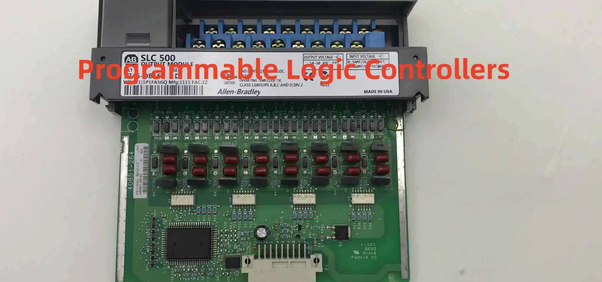
A programmable logic controller (PLC) is a digital computer used for automation of industrial processes, such as control of machinery on factory assembly lines. PLCs can be programmed to perform logical functions, timing, counting, arithmetic, and data handling tasks needed for controlling industrial equipment and processes.

PLCs have input and output devices that allow them to monitor and control machines and processes. The input devices collect data from sensors that measure things like temperature, pressure, speed, etc. The PLC then processes this data according to a program and determines what the output devices connected to it should do in response. The output devices can control actuators, valves, motors, lights, or other equipment.

History of PLCs

The origins of PLCs go back to the late 1960s when the automotive industry was seeking a way to replace complex relay-based control systems with a more flexible, software-driven approach. Engineers at General Motors (GM) developed the first PLC, introduced in 1968 under the trademarked name Programmable Logic Controller.

GM’s early PLCs used ladder logic diagrams, borrowing from the relay-based control systems they were replacing. Ladder logic made PLC programming more intuitive for engineers accustomed to working with electrical control schematics. The first PLCs had limited memory and logic compared to modern devices, but already offered major advantages in terms of flexibility, ease of programming, and reliability.

PLCs were soon adopted by other industries like steel mills, chemical plants, and food processing due to their ability to control complex systems safely and efficiently. As technology advanced, PLCs became more sophisticated and powerful. Early PLCs could only handle boolean (on/off) logic but later versions introduced more complex functions like timers, counters, arithmetic, and analog I/O handling.

Today’s PLCs are highly advanced computation and control devices capable of managing entire automated factories and processes with precision and reliability. Major PLC manufacturers include Allen-Bradley, Siemens, Mitsubishi, Omron, and Schneider Electric.

Benefits of Using PLCs

PLC IoT
PLC IoT

PLCs provide many benefits that make them invaluable for industrial automation and process control:

Flexibility – PLC logic can be reprogrammed when needed to make changes or implement improvements in the controlled system. This avoids having to rewire circuits or rebuild equipment when system changes are needed.

Reliability – PLCs are solid state devices with no moving parts that can operate for years in harsh industrial environments like dust, moisture, vibration, and extreme temperatures. This makes them highly reliable compared to electromechanical relays.

Scalability – Most PLCs can be expanded and reconfigured to add I/O points and capabilities. This allows the control system to grow over time as new sensors, processes, or equipment are added.

Ease of Programming – Ladder logic and other PLC programming languages are relatively easy to learn. Programs can be simulated on a PC before loading into the PLC. Troubleshooting and editing programs is straightforward.

Communication Capabilities – PLCs can communicate with other devices and controllers on local networks and larger distributed control systems. This allows coordination and monitoring across an entire automated facility.

Cost Effectiveness – Although the initial investment is higher than simple relays, PLCs offer very competitive long-term value given their flexibility, expandability, and durability.

Enhanced Control Capabilities – PLCs can implement advanced regulatory control, motion control, data acquisition, alarm handling, and other sophisticated automation functions beyond simple on/off control.

How PLCs Work

The basic operation of a PLC involves three primary functions:

  1. Input Scan – The PLC gathers input data from connected devices like sensors, switches, push buttons, etc. It examines the status of these input devices and saves their on/off states to memory.
  2. Program Scan – The PLC then executes the logic program, line-by-line, examining the input states and running any logic instructions programmed by the user. During this scan, the PLC may energize and de-energize internal relay coils based on programmed logic. The results or “solutions” are stored in memory.
  3. Output Scan – Finally, the PLC updates the physical output devices like motors, lights, valves, etc. based on the internal memory solutions from running the user program. The updated outputs then cause a change in the controlled process or machine.

These input-processing-output scans repeat many times per second to achieve real-time automation control. The PLC program determines exactly how the PLC will react to various inputs with appropriate outputs.

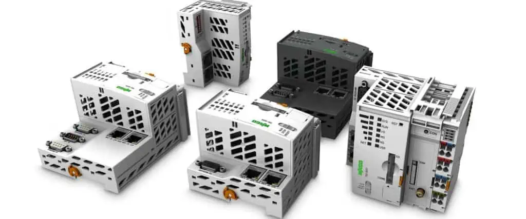
PLC Hardware Components

The main hardware components of a PLC include:

  • Processor – This is the central processing unit or “brain” containing the main memory, arithmetic logic unit (ALU), control unit, and instruction set to execute the PLC program.
  • Power Supply – Provides regulated DC power to the PLC processor, I/O modules, and field devices. Usually 24VDC.
  • I/O Modules – Interface between field devices and the PLC processor. Analog I/O modules convert sensor measurements to digital data. Discrete I/O modules convert device states to on/off signals the PLC understands.
  • Communication Modules – Allow the PLC to communicate with HMIs, data networks, remote I/O racks, and other devices. Common methods are Ethernet, serial, WiFi, and fieldbus modules like Profibus and Modbus.
  • Chassis or Backplane – Metal enclosure housing the processor, power supply, and I/O modules and providing internal communication buses.
  • Programming Device – Portable unit used to program the PLC. Can be a laptop, programming panel, or proprietary programmer. Connects to the PLC via USB, Ethernet, or other methods.

PLC Programming

PLCs are programmed using special software running on a PC or laptop. Programming involves three main steps:

  1. Design the program logic and enter via programming software.
  2. Simulate and debug program offline on the computer.
  3. Download tested program to the PLC for execution.

There are different techniques and languages used for PLC programming:

Ladder Logic

The most common PLC programming method which uses ladder diagrams based on circuit diagrams. Ladder logic has contacts, coils, instructions, and functions.

Example Ladder Rungs

Structured Text

Similar to Pascal programming language using statements, functions, variables, and other high level code structures.

Example Structured Text

Copy code

IF Level > 10 THEN Valve = Open ELSE Valve = Closed END_IF

Function Block Diagrams

Graphical language representing logic as interconnected function blocks. Used in continuous control systems.

Example Function Block

Instruction Lists

Low level basic instructions similar to assembly code. Not as commonly used today.

Example Instruction List

Copy code

LOAD Pressure GT 10 JMPC ValveOpen ValveClosed: MOV Valve, 0 JMP End ValveOpen: MOV Valve, 1 END:

Ladder logic is the most popular and widespread PLC programming language because it is easy to learn and mirrors old relay control schematics. But other languages are gaining use for more advanced functions.

Choosing a PLC

Factors to consider when selecting a PLC:

  • Number and type of I/O required (analog, digital, specialty modules)
  • Speed and memory needed
  • Communications requirements (networking, protocols)
  • Environmental conditions (temperature, humidity)
  • Programming preferences (ladder logic, instruction list, etc.)
  • Budget
  • Support and training available
  • Compatibility with existing and future systems
  • Reliability, reputation of manufacturer

Leading PLC manufacturers include:

  • Allen-Bradley (Rockwell)
  • Siemens
  • Schneider Electric
  • Mitsubishi
  • Omron
  • Beckhoff
  • Bosch Rexroth
  • Toshiba

It is best to select a PLC model that offers built-in room for expansion in case your I/O or program memory needs grow in the future. Getting the right PLC for an application involves balancing performance, capabilities, and cost.

PLC Communications

Modern PLCs communicate with many other devices and systems using a variety of networking methods and protocols. Communication capabilities a PLC may have include:

Programming – Used to upload/download programs from a PC to the PLC. Connections such as USB, Ethernet, RS-232, RS-485.

HMIs – Human-Machine Interfaces like industrial PCs and touch screens connected to a PLC to display system data and allow operators to monitor and control the process.

SCADA Systems – Supervisory Control and Data Acquisition systems connected to multiple PLCs and HMIs to monitor and control an entire factory or facility from a central computer.

Industrial Networks – PLC communication with other PLCs on high speed networks like Ethernet/IP, Modbus TCP, and EtherCAT to coordinate distributed control systems.

Fieldbuses – Connecting PLCs to remote I/O devices, drives, sensors using fieldbus networks like Profibus, Modbus RTU, and DeviceNet.

Wireless – Technologies like WiFi and cellular allowing PLCs to communicate wirelessly with mobile HMIs, data historians, asset management systems, and remote troubleshooting devices.

PLC Applications

PLCs are highly versatile devices used for automation in many industries and applications including:

IndustryApplication Examples
AutomotiveAssembly lines, conveyors, robotic welding, machine tools, painting
Food & BeverageMixing, bottling, canning, baking, bagging, automation lines
PharmaceuticalIngredient handling, mixing, packaging, labeling, inspection
PlasticsInjection molding, extrusion, blow molding, cutting, vision inspection
MetalsMetal stamping presses, CNC machines, welding, painting, plating
Oil & GasPipeline flow control, wellhead monitoring, refinery processing
PowerTurbine/generator control, substation automation, boiler control
LogisticsConveyor systems, pick-and-place, sorting, robotic handling
PackagingLabeling, sealing, wrapping, palletizing, cartoning

The flexibility, computing power, and communication capabilities of modern PLCs make them a fundamental component of automated systems in virtually all industrial sectors.

Advantages and Disadvantages of PLCs

Advantages:

  • Flexible, customizable programming
  • Reliable and rugged industrial computing platform
  • Built-in communications for networking and HMI connectivity
  • Scalable I/O configurations
  • Advanced capabilities beyond basic control (motion, data collection, etc)
  • Integrated diagnostics and troubleshooting
  • Mature technology with deep application knowledge base

Disadvantages:

  • Higher initial investment cost than simpler controls
  • Requires electrical design and programming skills
  • Advanced functions may require costly specialized modules
  • Troubleshooting problems requires specialized tools and training
  • Proprietary programming languages vary by manufacturer

The Future of Programmable Logic Controllers

PLCs will continue advancing in response to the needs for more sophisticated automation and “smart manufacturing” concepts. Key developments shaping the future of PLC technologies include:

  • Hardware advances – Smaller, more powerful, faster, cheaper PLCs with denser I/O and specialized modules
  • Increasing emphasis on software, connectivity, and remote access rather than just hardware logic
  • Use of PC-based controllers and soft PLCs running on industrial PCs
  • Programming enhancements integrating IEC 61131-3 languages with object-oriented extensions
  • Open source PLC platforms built on Raspberry Pi and Arduino
  • Integration of safety, motion control, vision, advanced math, and analytics into the PLC
  • IoT connectivity allowing PLC data access by mobile devices, cloud systems, and web dashboards
  • Cybersecurity enhancements to protect against threats to connected PLCs and plants
  • Machine learning incorporation for more adaptive analytics and predictive capabilities

PLCs will continue to evolve in ways that mirror computer technology trends while meeting industry needs for the best automation control technology.

Frequently Asked Questions

PLCC Package
PLCC Package

What are the most common types of sensors used with PLCs?

Some common industrial sensors interfaced to PLCs include:

  • Limit Switches – Detect position of moving part.
  • Photoelectric Sensors – Detect presence of objects.
  • Proximity Sensors – Detect nearness of objects without contact.
  • Temperature Sensors – Measure process temperatures.
  • Pressure Sensors – Measure liquid, gas, or hydraulic pressures.
  • Flow Sensors – Measure liquid or gas flow rates.
  • Level Sensors – Measure liquid levels in tanks or vessels.

What are the main advantages of PLCs over relay logic?

PLCs offer numerous advantages compared to traditional relay circuits:

  • Flexible programming that is easier to change
  • Much faster response and scan times
  • Not susceptible to contact issues like sticking or corrosion
  • Higher density I/O in smaller space
  • Communication and data collection abilities
  • Advanced capabilities beyond basic logic

How do you troubleshoot problems with a PLC?

Common techniques for troubleshooting PLC issues include:

  • Monitoring status LED indicators on modules
  • Checking I/O signals with a handheld digital tester
  • Verifying proper voltage at power supply and I/O modules
  • Uploading program to computer to check logic and spot errors
  • Monitoring PLC diagnostics memory addresses
  • Forcing inputs/outputs manually or inserting simulator signals
  • Checking communication connectivity and data flow
  • Comparing behavior to simulation programs or known good backups

What precautions are important when wiring inputs and outputs to a PLC?

Key wiring precautions include:

  • Separating AC power wires from DC I/O wiring
  • Properly grounding the PLC and field devices
  • Using shielded, twisted pair cables for analog signals
  • Avoiding running I/O wiring in parallel with power cords
  • Keeping wire lengths short to avoid electrical noise issues
  • Double checking wiring before energizing
  • Verifying rated voltage and current limits
  • Following all electrical safety procedures

How can better cybersecurity be ensured for PLC systems?

PLCs used for critical infrastructure need protections like:

  • Blocking unused communication ports
  • Disabling unnecessary services and protocols
  • Encrypting network traffic where possible
  • Using whitelisting to only allow authorized access
  • Proper password policies and access controls
  • Virtual private networks (VPNs) for remote access
  • Security tools like firewalls, intrusion detection, backups
  • Physical security restricting physical PLC access
  • Regular penetration testing to find vulnerabilities

Summary

Programmable logic controllers or PLCs are rugged, reliable computerized control systems used for automation in industrial applications. PLCs contain a processor, power supply, I/O modules, and communication modules housed in a chassis. Input devices like sensors are monitored by a PLC which then runs a logic program to determine the appropriate response from output actuators according to programmed instructions.

Ladder logic is the most common PLC programming language, but other methods like structured text and function block are also used. Leading PLC brands include Allen-Bradley, Siemens, Omron, and Mitsubishi. Choice of PLC depends on factors like number of I/O, speed, memory, and communications requirements.

PLCs provide flexible, scalable, and reliable control well-suited for harsh industrial environments. They offer advanced capabilities beyond what could be achieved with simple relays. Modern PLCs incorporate sophisticated communications, HMIs, motion control, safety systems, data collection, and more. PLCs will continue advancing in response to automation needs for IoT connectivity, machine learning, and other smart technologies.

How Does Automotive Alternator Work?

An alternator is a crucial component in modern automobiles that is responsible for generating electricity to power the electrical system while the engine is running. The alternator charges the battery and powers the ignition system, lights, entertainment systems and other electrical components.

Understanding how an automotive alternator works helps drivers appreciate this vital engine component. This article will provide a comprehensive overview of alternator design, function and operation.

What is an Automotive Alternator?

An alternator is an electrical generator that converts mechanical energy from the engine into electrical energy through electromagnetic induction. Alternators generate alternating current (AC) electricity which is then converted to the direct current (DC) electricity needed to charge the battery and power vehicle electronics.

The key components of an automotive alternator include:

  • Rotor – The rotating part consisting of a coil winding surrounding an iron core. It is mounted on the drive shaft and rotates within the stator.
  • Stator – The stationary part consisting of three sets of windings surrounding an iron core. When the rotor rotates, it induces alternating current in the stator which is fed to the diodes.
  • Diode Rectifier – Converts AC current generated in the stator to the DC current needed for the battery and vehicle system.
  • Voltage Regulator – Controls the field current to maintain a constant voltage output as engine RPM varies.
  • Brush Assembly – Contains slip rings and carbon brushes that conduct current to the rotor coil windings.
  • Cooling Fan – Cools the alternator to prevent overheating.
  • Front and Rear Housing – Contains the components and allows convenient mounting.

Diagram of the main components in a typical automotive alternator.

How Does an Automotive Alternator Produce Electricity?

Alternators generate electrical energy using the principles of electromagnetic induction discovered by Michael Faraday. Here are the key steps in the power generation process:

1. Mechanical Energy from the Engine

  • The alternator is belt-driven by the engine’s crankshaft via a serpentine belt. This rotates the rotor at engine speed.

2. Magnetic Field Induced in the Rotor

  • As the rotor spins, a small electric current is passed to the rotor windings through the slip rings and carbon brushes.
  • This creates a magnetic field around the rotor coils.

3. Alternating Current Induced in the Stator

  • As the rotor magnetic field rotates around the fixed stator windings, it induces an alternating current in the stator windings.
  • This is caused by Faraday’s Law of electromagnetic induction. Faster rotor motion induces greater voltage.

4. Conversion to Direct Current

  • The alternating current produced in the stator windings is converted into direct current by the diode rectifier bridge.
  • The rectifier uses semiconductor diodes which allow current to flow in only one direction resulting in DC output.

5. Voltage Regulation

  • The voltage regulator controls the rotor magnetic field strength to maintain a constant output voltage, typically around 14V, as engine rpm varies.
  • It senses voltage at the battery terminal and adjusts current flow into the rotor.

6. Battery Charging

  • The DC output current of the alternator recharges the vehicle’s battery. This provides electricity when the engine is off.
  • The battery acts as a voltage stabilizer smoothing out transients in alternator output.

This alternating current (AC) to direct current (DC) conversion process takes place continuously while the engine is running. This provides the electricity needed for proper vehicle operation.

Main Types of Automotive Alternators

While alternator designs vary by manufacturer and application, they typically fall into two main configurations:

Claw Pole Alternator

This uses a claw-shaped pole piece in the rotor rather than windings. The claw pole rotor is pressed onto the shaft and surrounded by the stator. Benefits include simple design, low cost and high efficiency. Claw pole alternators are common in many late model vehicles.

Wound Field Alternator

This uses an electromagnetic coil winding in the rotor for the magnetic field like a traditional generator. It allows variable control of the rotor field current, enabling better voltage regulation. Wound field alternators are more expensive but commonly used on older vehicles.

The claw pole design is dominant today due to its simplicity, performance and cost-effectiveness for high output electronic charging systems. However, both provide the essential DC electricity generation function.

Major Components of an Automotive Alternator

Now let’s take a closer look at the major components that make up a typical modern high-output alternator.

Rotor

This is the rotating component that generates a moving magnetic field to induce current in the stator windings.

  • On claw pole alternators, the rotor consists of a steel claw-shaped pole piece pressed and shrink-fitted onto an iron core which is mounted on the driveshaft.
  • On wound field alternators, the rotor uses coil windings fed with DC current to generate the magnetic field.
  • The rotor spins within the fixed stator, typically at up to 15,000 rpm on engine speeds. Faster rotor speed induces higher voltage in stator.

Stator

The stator is the stationary component containing electrical windings surrounding an iron core. The windings are composed of copper wire coils that are placed into slots in the laminated core.

  • The stator core is made of many thin steel laminations for low hysteresis losses.
  • The stator windings generate three-phase alternating current when rotating magnetic field of rotor sweeps past them.
  • Each stator winding is connected to the rectifier diodes to convert AC to DC output current.

Diode Rectifier

The diode rectifier bridge converts the AC voltage generated in the stator windings into the DC voltage needed for the vehicle electrical system.

  • It contains six diodes arranged as a bridge circuit. Each diode allows current flow in only one direction.
  • The diodes only allow the half of the AC cycles where current flows towards the battery to pass, resulting in DC pulses.
  • The rectifier is typically mounted on the alternator rear housing. Diodes are actively cooled to handle high current.

Voltage Regulator

The voltage regulator controls the field current entering the rotor to generate the required voltage output.

  • It monitors battery voltage through a sensing wire connected to the battery terminal.
  • When output voltage drops below the target level (e.g. 14V), the regulator increases field current which boosts induced voltage.
  • This process keeps output voltage constant even as rotor speed varies with changing engine rpm.
  • The regulator may be mounted internally or externally. Modern alternators have built-in regulators.

Brush Assembly

Brushes conduct electric current between the spinning rotor and the stationary contacts.

  • Slip rings mounted on the rotor shaft are contacted by carbon brushes which have spring loading tension.
  • Current is conducted through the brushes to excite the rotor magnetic field. Brushes wear over time and need periodic inspection.
  • Brush assembly design aims to maximize contact surface area for high current and minimal friction.

Cooling Fans & Vents

Fans and vents provide critical cooling air circulation over and through the alternator.

  • Cooling fans pull in outside air, improving heat dissipation from hot components.
  • Vents allow air flow to reach internal components like diodes and windings.
  • Proper cooling prevents alternator failure from overheating which reduces output.

Front & Rear Housings

  • Sturdy front and rear die-cast aluminum housings enclose and protect the alternator components.
  • They have mounting points to install the alternator on the engine securely.
  • The housings allow easy access when disassembling the alternator for servicing.
  • Vents, cooling fans and other attachments bolt on to the housings.

Alternator Design Variations

While the basic components described above make up the core of most automotive alternators, there can be variations in design:

  • Single or Dual-Voltage – Some alternators have switchable voltage settings for 12V or 24V system applications.
  • External or Internal Regulator – Older alternators had external regulators while modern ones have built-in regulators.
  • Lundell and Salisbury Pole Rotors – Based on the shape and construction of the rotor pole pieces. Salisbury type has lower magnetic losses.
  • Number of Stator Windings – Can be 12-pole or 24-pole stator designs. More poles typically means higher output current.
  • Claw Pole or Wound Field – Fundamental rotor design difference as described earlier.
  • Diode Bridge Design – Diode count, arrangement and cooling method can differ. Some use hybrid bridge regulators.
  • Brush Configuration – Brush quantity, materials, tensioning and slip ring design affect performance.

So while basic working principle remains the same, alternators are engineered with variations to provide optimized performance for different vehicles and applications.

Alternator Drive Methods

Automotive Alternator

Output current capacity is directly related to how fast the alternator spins. Therefore, proper drive design is critical. Here are the main alternator drive types:

Belt Drive

  • Most common method using a serpentine v-belt running on pulleys connected to the crankshaft and alternator.
  • Typically drive ratio of 2.5 to 3:1 relative to crank. Turning at engine idle speed generates sufficient voltage.
  • Needs proper belt tension. Over or under-tightening reduces output and belt life.

Chain Drive

  • Roller chain drive can be more durable and withstand higher loads than belt drive.
  • Allows greater distance between crank and alternator mounting points.
  • Requires periodic chain tensioning adjustment and lubrication.
  • Noisy operation and cost make it less common than belt drive today.

Gear Drive

  • Spur gearset provides constant meshing for robust drive and fixed ratio speed increase.
  • Allows very high speed alternator shaft rotation up to 24,000rpm for max output.
  • Needs precision gear machining and can be noisy in operation.
  • Added cost limits use to high performance and racing applications.

Proper belt tensioning with idler pulleys is the most common and cost-effective drive today. But other drive options allow ultra-high output when needed.

How Voltage Output is Controlled

Maintaining steady charging system voltage as engine rpm varies is critical to avoid overcharging or undercharging the battery. Here’s how voltage regulation works:

Sensing Battery Voltage

  • The voltage regulator monitors battery voltage through a sense wire connected to the positive terminal.
  • If output voltage drops below the desired level, typically around 14 volts, the regulator activates.

Adjusting Field Current

  • The regulator can electronically adjust current flow into the rotor field winding.
  • Higher current strengthens rotor magnetic field which induces higher AC voltage in stator.
  • Lower current weakens rotor field and decreases AC voltage generation.

Maintaining Constant Output Voltage

  • By controlling rotor field current, the charging voltage can be held steady even as engine rpm changes.
  • This prevents excessive or inadequate charging as driving conditions vary.
  • If external power loads are added, the regulator further boosts field current to compensate load.

Limiting Maximum Voltage

  • The regulator has overload protection if voltage spikes occur.
  • It limits maximum field current input to prevent dangerously high voltage generation.
  • This protection prevents damage to vehicle electronics from voltage surges.

Modern electronic regulators allow very precise and responsive voltage control tailored to match alternator design and output curves.

Alternator Charging Process Explained

Let’s walk through the key steps that take place as the alternator charges the battery:

  1. Engine cranking rotates alternator rotor through drive belt. Rotor magnetic field is initially residual.
  2. As rotor picks up speed, residual magnetism generates small AC voltage in stator windings.
  3. Initial AC is converted to DC by rectifier diodes. This begins charging the battery which applies DC to rotor through brushes.
  4. Rotor electromagnetism builds up from battery current flow through windings. Rotor field strengthens.
  5. Stronger rotor magnetic field induces higher AC voltage in stator as it cuts across windings faster.
  6. Higher AC voltage is rectified into stronger DC output. Battery charges faster and sends more current to rotor.
  7. The cycle escalates until nominal voltage level is achieved, typically 14V. Regulator then holds it steady.
  8. If battery state of charge decreases, regulator boosts rotor field current to increase output voltage to recharge.

This self-exciting process automatically builds charging voltage to the preset target level needed to keep the battery fully charged.

Troubleshooting Alternator Problems

Here are some common symptoms indicating alternator issues and likely causes:

Dead Battery

Fully discharged battery while driving points to the alternator not charging properly.

  • Check for loose, broken or slipping drive belt. Tighten belt to spec.
  • Inspect for poor wiring connections, damaged diodes or faulty voltage regulator.
  • Test that rotor produces adequate magnetic field. Check brushes and slip rings.
  • If battery keeps going dead, test alternator output voltage. Might need rebuild or replacement.

Dimming Headlights

If headlights and other lights dim noticeably at idle but brighten when revved, the alternator is weak.

  • Belt may be loose or worn. Adjust belt tension.
  • Faulty diodes, stator windings or regulator may need replacement.
  • Check for high resistance on power output terminal causing voltage drop.

Whining Noise

High pitched whining or squealing noises usually come from drive belt or bearing issues.

  • If noise varies with revs, belt is likely loose or misaligned on pulleys.
  • Adjust belt tension or alignment. Replace belt if worn or glazed.
  • Constant noise indicates worn bearings starting to fail. Alternator rebuild needed.

Smell or Smoke

Burning smell or visible smoke/sparks points to severe internal overheating failure.

  • Immediately shut off engine to prevent greater damage.
  • Check for jammed cooling fans, blocked ventilation and debris buildup causing overheating.
  • Severe faults like grounded windings require complete alternator replacement.

Early detection of minor issues based on unusual noises, smells or operating changes can help prevent more extensive damage and avoid breakdowns.

Alternator Maintenance Tips

Routine prevention maintenance is key to maximize longevity of your vehicle’s alternator. Follow these alternator care tips:

  • Check drive belt – Inspect belt periodically for cracks, glazing, fraying and tension. Replace belt if worn.
  • Check belt alignment – Make sure belt runs straight on alternator, crank and idler pulleys. Misalignment causes excess wear.
  • Check mounts – Ensure alternator mounting brackets are tight and free of cracks. Loose mounts cause misalignment.
  • Check wiring – Clean and tighten electrical connections, especially positive and negative output terminals. Fix damaged wiring insulation.
  • Check ventilation – Ensure cooling air ducts, fans and ventilation holes are not blocked by dirt or debris.
  • Listen for noise – Take note of any unusual grinding, squealing or bearing rattle noises which indicate wear.
  • Consider overhaul – For higher mileage vehicles, having the alternator rebuilt periodically will extend its life.
  • Test output annually – Use a digital multimeter once a year to verify alternator is generating proper voltage.

Well-maintained alternators can last 150,000 miles or more. But neglecting basic component checks increases the chances of being left stranded when it fails.

Alternator Output Testing

If you suspect charging system issues, alternator output voltage and amperage should be tested. Here is one common testing method:

Test Equipment Needed

  • Digital multimeter (DMM) with DC voltage and current capacity
  • Jumper wires with alligator clips
  • Load bank (such as a 12V headlamp)

Testing Procedure

  1. Attach positive (red) DMM lead to alternator output terminal nut and negative (black) lead to battery negative terminal.
  2. With engine off and keys out of ignition, check battery voltage. A well-charged battery will show 12.4 – 12.6V.
  3. Start engine and turn on all loads (headlights, blower fan, rear defogger etc). Run engine at 1500 rpm.
  4. Measure voltage at alternator output terminal again. Should show approx. 14V. If not, regulator may be faulty.
  5. Turn off all loads. Then turn on load bank connected to battery positive terminal.
  6. Gradually increase load resistance while observing amp output. Output should increase to meet demand.
  7. Check for smooth voltage regulation back to 14V after load is removed. Erratic voltage indicates faulty diodes or bad rotor ground.
  8. If output voltage or amperage is outside spec, the alternator may need overhaul or replacement. Consult a shop.

This test procedure checks key characteristics to determine if the alternator is performing properly or if repairs are needed.

What is Micro-electromechanical Systems (MEMS) ?

rf antenna chip

Introduction

Micro-electromechanical systems, or MEMS, are tiny integrated devices that combine mechanical and electrical components on a common silicon substrate. MEMS extend the fabrication techniques developed for the integrated circuit industry to add mechanical elements like beams, gears, diaphragms, and springs to chips.

In this comprehensive guide, we will cover:

  • The components and operating principles of MEMS devices
  • Various types of MEMS sensors, actuators, and other applications
  • MEMS materials, manufacturing processes, and packaging
  • Design and simulation considerations for MEMS
  • Current and future applications using MEMS
  • MEMS industry landscape and key players
  • Advantages and challenges with MEMS technology
  • FAQs

By the end, you’ll have a solid grasp of what micro-electromechanical systems are, how they work, where they are used, and their impact. Let’s get started!

Components and Operating Principles of MEMS

common examples of MEMS

Micro-electromechanical systems integrate miniature:

  • Sensors – To detect physical phenomena like motion, pressure, chemical levels, etc. Common examples include accelerometers, gyroscopes, pressure sensors, and gas sensors.
  • Actuators – To provide physical movement or action. Examples include micromirror arrays, valves, pumps, and manipulators.
  • Electronics – To process signals from sensors and control actuators. The circuitry includes components like ASICs, capacitors, transistors, and bond pads.
  • Mechanical Structures – The micromachined components that enable physical functionality like cantilevers, gears, membranes, channels, and diaphragms.

By combining these miniaturized elements on a chip, MEMS enable new categories of tiny sensors, actuated devices, and integrated systems not achievable with conventional electronics.

MEMS operate through principles like:

  • Thermal actuation
  • Piezoelectric transduction
  • Capacitive sensing
  • Electrostatic actuation
  • Resonant energy harvesting
  • Microfluidic control

These enable functions difficult to implement conventionally at such small scales. Cutting edge fabrication techniques make MEMS possible.

Types of MEMS Devices

There are several major categories of MEMS devices:

MEMS Sensors

Sensors detect physical phenomena and convert them into electronic signals for processing.

Accelerometers – For measuring acceleration and tilt along 1, 2 or 3 axes. Critical for airbags, phones, navigation, vibrations, and more.

Gyroscopes – Measure angular velocity and orientation in space. Used in drones, VR/AR, robotics, and other applications needing precision orientation.

Pressure Sensors – Gauge applied pressure. Used in weather monitoring, touchscreens, biomedical devices, and more.

Chemical Sensors – Detect gaseous chemicals and concentrations. Enable smart gas detection and analysis.

Inertial Measurement Units – Combine accelerometers and gyroscopes to precisely track motion and orientation for navigation and guidance.

Resonant Sensors – Vibrating MEMS structures shift frequency based on mass or other changes, allowing extremely precise measurements.

MEMS Actuators

Actuators provide movement or mechanical action. Examples include:

Micromirror Arrays – Control light beams by tilting tiny mirrors for displays, scanning, and fiber optics.

Microvalves – Regulate fluid flows in miniature channels and pipes. Used in miniature gas chromatography systems, lab-on-a-chip devices, etc.

Optical Switching – Route optical signals between fiber optic channels. Used in telecommunications and data networking equipment.

RF MEMS Switches – Switch high frequency electrical signals for tuned impedance matching and signal routing. Used in tunable filters, phased arrays, and reconfigurable antennas.

Microspeakers – Vibrate to generate sound waves and audio output. Used in earphones and integrated device sound.

MEMS Pumps – Generate controlled microfluidic flows or pressure differentials. Used for drug delivery, analyte sampling, microcooling systems, etc.

Other Types of MEMS

Beyond sensors and actuators, other types of MEMS include:

  • Microfuel cells – Generate electricity from fuel sources through electrochemical reactions on a chip.
  • Micromotors – Spin tiny rotors using electromagnetic forces or thermal actuation. Used for micro gears, pumps, and other mechanisms.
  • Microbolometers – Measure infrared radiation for thermal imaging applications. Used in fire detection, autonomous vehicles, and security cameras.
  • Microneedle patches – Contain arrays of microneedles for drug delivery through the skin.

The diversity of MEMS devices enables sophisticated miniature systems across a huge range of applications, as we’ll explore next.

MEMS Materials and Manufacturing Processes

Fabricating MEMS requires specialized processes, equipment, and materials. Key aspects include:

Substrate Materials

  • Silicon is the most common substrate material due to well-controlled microfabrication techniques developed by the IC industry.
  • Other options include glass, ceramics, metals, and polymers.

Deposition Processes

  • Depositing thin films of structural and sacrificial materials through processes like chemical vapor deposition (CVD), sputtering, and molecular beam epitaxy.

Lithography

  • Patterning masks and exposing photoresists using techniques like photolithography, e-beam lithography, and X-ray lithography.

Etching

  • Removing material selectively through wet etching with acid solutions or dry etching using plasma.

Doping

  • Ion implantation and diffusion to dope structural layers like polysilicon with boron, phosphorus or other dopants.

Bonding

  • Anodic bonding of micromachined silicon wafers with glass layers.

Micromachining

  • Bulk micromachining to selectively etch inside silicon or other substrates.
  • Surface micromachining to build structures by patterning layers on top of the substrate.

Careful sequencing of these microfabrication steps allows constructing the mechanical and electrical components needed for MEMS.

MEMS Packaging

Once fabricated, MEMS dies require specialized packaging to:

  • Protect delicate MEMS structures from damage
  • Facilitate required gas or fluid flows
  • Allow space for movements
  • Electrically connect bond pads
  • Mount components like application-specific integrated circuits (ASICs)
  • Enable integration into larger systems

Common packaging approaches include:

  • Ceramic and plastic packaging
  • Wafer-level packaging and encapsulation
  • Multi-chip module packaging
  • Printed circuit board integration

Innovations in MEMS packaging continue advancing capabilities while reducing size and cost.

MEMS Design and Simulation

Designing MEMS requires cross-functional physics simulation and modeling tools. Key analyses performed include:

  • Mechanical – Stress, vibration, fatigue life, resilience, etc.
  • Electrical – Drive circuitry, feedback signals, noise, etc.
  • Thermal – Heat dissipation, thermal lags, conduction, etc.
  • Fluidic – Air/liquid flows, pressure differentials, turbulence, etc.
  • Optical – Light reflection, diffraction, scattering, etc.

Each MEMS application has unique multiphysics requirements that must be modeled across mechanical, electrical, fluidic, and thermal domains synergetically.

Standard 3D CAD tools combined with multiphysics solvers address MEMS modeling needs for precision design optimization.

Current and Future Applications of MEMS Technology

Thanks to their tiny size, low cost, and sophisticated functionality, MEMS devices are enabling innovative applications across every industry:

Transportation – Inertial guidance, ESP, safety sensors in airbags, tire pressure monitoring, etc.

Consumer Electronics – Accelerometers, gyroscopes, microphones, and displays in smartphones, game consoles, etc.

Medical – MEMS pressure sensors in catheters, microneedle drug delivery, implants, diagnostics.

Industrial – MEMS accelerometers for vibration monitoring, gas sensors for leak detection, microvalves for control.

Defense – MEMS inertial measurement units in missiles and drones, chemical threat detection, research into MEMS robots and smart dust.

Scientific – Lab-on-a-chip devices, microanalysis systems, portable microsensors.

Communications – RF MEMS switches for tuned antennas, optical routing, phase array transmitters.

Auto – Tire pressure sensors, inertial sensors, infrared detectors for night vision systems.

The next wave of innovation in self-driving vehicles, IoT devices, AR/VR, Industry 4.0, and more will be enabled by MEMS. The opportunities are boundless thanks to the unique capabilities MEMS provide.

MEMS Industry Landscape

MEMS
MEMS

The global MEMS industry is projected to grow to around $90 billion by 2025. Key players include:

  • Semiconductor foundries like TSMC, GlobalFoundries, and SMIC that fabricate MEMS devices.
  • Fabless MEMS designers including STMicroelectronics, Bosch Sensortec, InvenSense, and mCube.
  • IDMs with internal MEMS manufacturing like Texas Instruments and Analog Devices.
  • Applied Materials, SUSS MicroTec, and DISCO providing fabrication equipment.
  • OSATs packaging and testing MEMS including ASE, Amkor, and JCET.
  • Automotive Tier 1s producing MEMS sensors for vehicles, such as Denso, Delphi, and Infineon.

While initially driven by a small group of IDMs, todayโ€™s MEMS industry involves an advanced supply chain enabling high volume foundry production. Economies of scale continue driving increased adoption.

Advantages and Challenges of MEMS

Some key benefits MEMS provide versus conventional implementations:

Benefits

  • Extreme miniaturization impossible through other means
  • Fully integrated devices combining electronics and mechanical elements
  • Low power consumption due to reduced size
  • Cost effective high-volume fabrication
  • Performance improvements from scaling effects

Challenges

  • High development costs and long design cycles
  • Need for advanced modeling and simulation skills
  • Strict process controls and expertise required
  • Packaging for protection while allowing operation
  • Metrology of 3D microscopic features

By capitalizing on their advantages while navigating inherent challenges, MEMS stand to revolutionize nearly every industry much like ICs did for electronics.

Frequently Asked Questions

Here are some common MEMS-related questions:

Q: How small are MEMS devices typically?

A: MEMS range from 20 micrometers to 1 millimeter. Very small yet large enough to allow practical microfabrication. State-of-art processes steadily allow smaller MEMS over time.

Q: How are MEMS different from ICs?

A: While fabricated similarly to ICs, MEMS add physical micromechanical structures rather than just electronic circuits. This allows mechanical sensing and actuation.

Q: Are MEMS always made from silicon?

A: Most use silicon substrates due to readily available silicon micromachining techniques from the IC industry. But some MEMS leverage materials like polymers.

Q: How durable and reliable are MEMS components?

A: MEMS can last decades in many applications with careful design. However, certain environments with high temperatures, pressures, radiation or contaminants can impact reliability.

Q: Are MEMS expensive to produce?

A: MEMS fabrication has high upfront costs for masks and process development. However, the per unit costs become very affordable in high volume thanks to batch manufacturing principles.

Conclusion

In summary, micro-electromechanical systems fuse electrical and mechanical components on integrated chips to enable transformative applications. With ongoing innovations in manufacturing and design, MEMS will continue growing as a key technology across industries from automotive to medical to consumer electronics and more. Their unique advantages of microscopic size, integration, low cost, and sophisticated performance open up new possibilities. While engineering MEMS requires specialized expertise, the benefits make the investment well worth it for next-generation products and capabilities.

Finger Print Lock Appliactions,Design and Manufacturing

Introduction

Fingerprint locks, also known as biometric fingerprint locks, are access control devices that use fingerprint recognition technology for locking and unlocking doors, drawers, lockers and more. They offer a convenient and secure unlocking solution compared to keys or combination locks.

In this comprehensive guide, we’ll cover:

  • Applications of fingerprint locks
  • How fingerprint lock technology works
  • Design considerations for fingerprint locks
    • Sensor types
    • Processing
    • Matching algorithms
    • Power options
    • Enclosure design
  • Manufacturing and assembly of components
  • Testing and calibration best practices
  • Advancements in fingerprint locks
  • FAQs

By the end, you’ll understand the full process of engineering fingerprint locks from initial applications, through design, manufacturing, and testing to bring reliable biometric products to market. Let’s get started!

Applications of Fingerprint Locks

Fingerprint locks are used in a diverse range of applications including:

  • Homes and apartments
  • Offices and workspaces
  • Schools and universities
  • Hotels and hospitality
  • Residential care facilities
  • Gyms and sporting venues
  • Laboratories
  • Hospitals and healthcare
  • Law enforcement facilities
  • Financial institutions
  • Sensitive industrial sites

They provide convenient access control in virtually any environment where managing keys or remembering codes poses challenges. Users simply enroll their fingerprint once then unlock reliably and instantly.

Next, we’ll take a technical look inside fingerprint lock design and operation.

How Fingerprint Lock Technology Works

Fingerprint locks function using the following key stages:

Fingerprint Capture

The user places their finger on the fingerprint sensor. The sensor images the fingertip and captures the fingerprint pattern.

Processing

The processor digitizes the fingerprint image and extracts unique minutiae points as a mathematical representation.

Fingerprint Matching

The extracted fingerprint data gets compared to stored enrollment templates for a match. Advanced matching algorithms are used.

Access Granted

If a match score exceeds the set threshold, the identity is verified and the lock grants access. The door or safe unlocks.

Storage

Users’ enrollment templates get stored in a protected local memory within the lock. Templates should be encrypted.

This provides a high-level overview of key subsystems in a fingerprint lock. Next we’ll look at design considerations and options for each area.

Fingerprint Lock Design Considerations

Designing an effective, reliable fingerprint lock involves careful selection of:

Fingerprint Sensor Type

Two main sensor technologies:

Optical – Uses a camera with illumination to image the fingertip surface. Offers good image quality if sized adequately.

Capacitive – Senses fingerprint ridges using an array tiny capacitors. Compact but more prone to environment impact.

Key tradeoffs: Image quality vs. size. Capacitive suitable for small locks if calibrated well. Optical preferred for highest accuracy in all conditions.

Processing Hardware

A microcontroller or microprocessor is required to process the raw sensor image, extract features, match against templates, control peripherals, etc.

Key factors: Sufficient performance for image processing and matching algorithms, crypto functions for template security, interfaces for peripherals, low power operation. ARM Cortex M4 or faster 32-bit MCUs are commonly used.

Matching Algorithms

The algorithm used to compare the live fingerprint against enrolled templates is crucial for reliable recognition.

Common matching approaches: Minutiae based, ridge feature based, image correlation, machine learning based. A hybrid approach combining minutiae with other advanced techniques often performs best.

Power Supply

A stable, reliable power source is required. Can use:

  • Internal batteries
  • External AC adapter
  • USB power

Battery is convenient but may require periodic charging/replacement. AC powered locks avoid battery issues but need outlet access.

Enclosure

The lock housing must:

  • Protect internal electronics
  • Mount sensor ergonomically
  • Provide mechanical locks/latches
  • Allow accessible wiring
  • Withstand use, weather, tampering

Material, seals, construction must balance function, cost and aesthetics.

Careful engineering of all subsystems results in a robust, usable fingerprint lock that provides convenient biometric access control. Next we’ll look at manufacturing critical components.

Fingerprint Lock Manufacturing and Assembly

Producing reliable fingerprint locks requires close attention during:

Sensor Manufacturing

The image sensor integrated circuit fabrication process must achieve:

  • High pixel density for detailed imaging
  • Low defect rates to avoid bad pixel clusters
  • ESD protection for fingerprint static discharges

The silicon fabrication facility must maintain extremely clean conditions.

For capacitive sensors, the capacitor array geometry must be uniformly micro-etched with tight alignment.

Processor Sourcing

The processor is typically sourced as a completed IC component. Key aspects:

  • Sourcing from reputable manufacturers like STM, NXP, or ATMEL
  • Order sufficient volume to qualify wafer lot and obtain consistent quality
  • Rigorously validate received units for defects before assembly

Matching Algorithm Optimization

Extensively tuning matching parameters and testing recognition accuracy using datasets of real fingerprints is key.

Lock Assembly

Proper assembly protocols must be followed:

  • ESD control procedures to avoid static discharge damage
  • Component placement following layout design rules
  • Process validations e.g. torque requirements for enclosure screws
  • Periodic quality audits on units from production line

With rigorous manufacturing practices for critical subsystems, reliably functioning fingerprint locks can be produced at scale.

Testing and Calibration Best Practices

To confirm locks operate properly prior to delivery, key testing and calibration steps include:

Unit Testing

  • Verify all electronic components functional
  • Validate processor execution timing
  • Check current draws and power consumption
  • Confirm wired/wireless interfaces working

Sensor Testing

  • Inspect image quality – sharpness, artifacts, distortions
  • Check live finger imaging reliability across conditions
  • Evaluate max image size and resolution

Matching Accuracy Testing

  • Test false reject rate with good fingerprints
  • Validate low false accept rate on invalid fingerprints
  • Tune matching thresholds as needed

Environmental Testing

  • Hot and cold exposure
  • Drop/shock/vibration resilience
  • IP rating validation if relevant

User Testing

  • Sample users enroll and unlock with live fingers
  • Identify any usability pain points

Extensive testing ensures consistent performance and quality for end customers.

Advancements in Fingerprint Lock Technology

Fingerprint lock technology continues advancing:

  • Multimodal – Combining fingerprint sensing with face, iris or other biometrics for multifactor authentication.
  • Anti-Spoofing – Detecting fake fingerprints made from silicon molds etc. Liveness detection can use multispectral imaging and deep learning algorithms.
  • Cryptography – Implementing highly secure methods to store fingerprint data as digital keys unlocks cloud-based access control frameworks.
  • Smart Home Integration – Connecting biometric locks into smart home systems for features like temporary access codes and centralized manageability.
  • Mobile Credentials – Using fingerprints matched on a smartphone in place of direct fingerprint enrollment in each individual lock.

Innovations like these will expand the capabilities and applications for fingerprint lock technology.

Frequently Asked Questions

Here are some common questions about fingerprint locks:

Q: Are fingerprint locks suitable for exterior doors?

A: Special waterproof fingerprint locks are available for exterior installation. However, they are less convenient than interior locks since users need to reach outside.

Q: How many fingerprints can be stored in a fingerprint lock?

A: Basic locks store up to 20-50 templates. More advanced locks support 100+ users. This depends on available memory and matching algorithm efficiency.

Q: What authentication options do fingerprint locks have if fingerprint recognition fails?

A: Locks normally support password or RFID card fallback authentication in case of fingerprint sensing issues.

Q: How are fingerprint locks powered?

A: Small batteries, USB or external AC adapter are common. Batteries provide convenient installation but require occasional replacement.

Q: How reliable are fingerprint locks compared to keyed locks?

A: Modern fingerprint locks with advanced sensors and algorithms can actually be more reliable than keyed locks which are susceptible to wear, mechanical issues or lost keys.

Conclusion

In summary, properly engineered fingerprint locks provide convenient, secure access control for a diverse range of applications from corporate offices to private residences.

Critical aspects like the fingerprint sensor, biometric matching algorithms, robust electronics, and calibrated assembly must be carefully designed and manufactured for reliable functionality. Extensive testing across conditions ensures optimal performance.

With innovative advancements in technology like anti-spoofing and smart home integration, fingerprint locks will continue enhancing security and convenience in access control implementations.

The Finger Print Locks design solution

In this modern era, nothing can be declared as completely secure. Locks are picked, safe are breakable, and even passwords are guessable. Therefore, such a device is needed which can provide sense of security. For the purpose of security, numerous things can be utilized such as iris, biometrics, and face detective systems etc. All the three mentioned systems are almost impossible to break. The finger print lock is a device which must be used now a days for securing houses, shops, and offices. A finger print lock is only unlocked with finger of a specific person. The finger print locks come in a variety of designs.

YouTube video
Fingerprint Lock factory

The Reasons why Finger Prints are Unique

It is an obvious fact that each person has fingerprints. The fingerprints are actually the small ridges which are frictional in nature which makes it easier for a person to hold stuff. These fingerprints are being used for the security purpose because their pattern is unique for every individual. The fingerprints remains in its original shape forever, however in cases of severe accidents and burns it vanishes off. As a matter of fact, finger prints are unique for each individual and therefore through sensors its pattern can be acquired and used for making safe locks which are unbreakable. However, these locks are electronic in nature and requires a power bank or battery for its working. There is a small sensor on to which a specific finger is placed. The sensor is then detecting the fingerprint pattern and open up the lock if it matches the pattern saved in its memory, else it generates an alarm for false attempt.

Finger Prints PCBA

The Process of Enrollment and Verification of Fingerprints

Before the operation of the fingerprint locks you are required to put in the pattern of prints of the person who will be in charge of the security of a specific vicinity. The finger prints of the specific person are first saved in the memory of the lock.

The Process of Enrollment and Verification of Fingerprints

There are two processes for the purpose and each has its own importance. First stage is known as enrollment and the second stage is known as verification. The enrollment step is dealing with the system to learn the patterns of the specific person to be recognize. Some locks are supporting a single pattern while some are supporting more than one pattern recognition. Fingerprints of each person who would deal with the lock are scanned and analyzed and then saved in to the memory of the lock in a coded form which is unbreakable and secure as well. It takes a little time for the process of enrollment.

enrollment step Fingerprints pcba

The next step is verification when the lock is ready to be used. During this stage a person is attempting to open the closed lock. Now if the fingerprint on the sensor of the lock is authenticated, the lock will open up, however if not authenticated the lock will either generate alarm or will remain closed. Some locks are having specific number of attempts for wrong authentication. For instance, if a lock is having 3 attempts, then after 3 wrong authentication the lock will go in idle mode and will not be usable for some specific time encoded in its chip e.g. 1 hour etc.

verification PCBA

The Process of Storage and Comparison of Fingerprints

The fingerprints were only used in the criminal investigations in beginning, however gradually it came out to be best for using in security. When computer is checking the fingerprints, it does it by pattern recognition but not manually through a magnifying glass. The comparison among the fingerprints is made among the one which is already stored in the system or memory of the lock and the once which sensor has acquired from the person trying to unlock it. This is done through its comparison with feature known as minutiae which is taken at the time of enrollment and verification steps.

The fingerprints

The computer is basically measuring the distances as well as angles among the different prints of the finger through feature of minutiae. This all done through the help of a computer based algorithm known as unique numeric code. The uniqueness of the fingerprints is measured through comparison and the right pattern is detected and the access of the lock is granted.

The Working of Fingerprint Lock

You may have observed the phenomenon of taking fingerprints on a paper i.e. dipping finger in to an ink pad and then pressing it against paper for having its clear image. The prints are also stored in the computer in the same way but through sophisticated techniques. First of all the computer is scanning the entire surface area of the finger and converting in to a code. The sensor or scanner is an optical one which is working with a bright light taken through the finger and taking its photograph in digital format.

The Working of Fingerprint Lock

The process is somehow different from taking a simple photograph as it has a simple method of flashing through surface and taking its image. The sensor is catching the exact and required amount of the detail of the finger such as contrast and brightness. The ridges of the finger with all necessary details are precisely taken and then matched with one stored in database or memory of the lock. Quality control is one of the major factor of the fingerprint locks.

fingerprint locks

The following are major points.

  • 1- First of all the LEDs beneath the scanner are putting bright light on glass of scanner for taking clean picture of finger.
  • 2- Remember, some locks are taking more time for the capturing of picture for a bright and crisp image.
  • 3- An algorithm is testing the image taken from the sensor with one stored in database through pattern recognition algorithm.
  • 4- The algorithm is calculating the distances among ridges and then comparing with stored image.
  • 5- Once both images are matched then the lock is given autonomy to get open and access is granted for the person putting fingers on lock.
  • 6- In case of denial of the fingerprint, lock is either generating alarm or submerge to idle mode for a specific time and some locks have message service which sends a message to the owner of the vicinity for false attempt of access to lock.

Rayming provide Finger Print Locks design solution services including pcb manufacturing or prototoype pcb assembly services , you can get pcb assembly board Welcome to send mail to sales@raypcb.com , Get good price now !

Top 15 Industrial Robots in The World

Robots in Industries

Introduction

Industrial robots are transforming manufacturing and automation across industries ranging from automotive to healthcare. With their ability to precisely and tirelessly perform complex tasks, industrial robots provide huge efficiency and quality benefits.

There are hundreds of industrial robot models available from technology providers worldwide. In this guide, we will highlight the top 15 industrial robots that are driving innovation in manufacturing and reshaping industry. For each model, weโ€™ll cover:

  • Intended applications
  • Key capabilities and specifications
  • Unique strengths
  • Manufacturer overview
  • Example implementations

By the end, youโ€™ll have a solid understanding of the leading industrial robots that are making an impact on manufacturing today. Letโ€™s get started!

Top 15 Industrial Robots

1. FANUC LR Mate 200iD

The LR Mate 200iD from FANUC is one of their most popular table-top industrial robots suitable for lightweight material handling and assembly.

Applications: machine tending, pick and place, inspection, pharmaceuticals

Payload: 7 kg reach 600 mm

Key Features: Long-term precision, reliable Japanese quality, easy programming

Company: FANUC is one of the largest global industrial robot manufacturers. Over 25% of industrial robots worldwide are FANUC robots.

Example Use: Ford uses LR Mate robots for engine subassembly manufacturing.

2. ABB IRB 460

ABB IRB 460 is a fast and flexible palletizing robot ideal for packaging and stacking applications.

Applications: Palletizing, pick and place, stacking, packaging

Payload: 60 kg reach 2.55 m

Key Features: High speed, four-axis flexibility, robust for harsh environments, easy programming

Company: ABB is a global leader in industrial automation and robotics manufacturing.

Example Use: Picturehouse Cinemas uses an IRB 460 robot to automatically stack soft drink cups.

3. KUKA KR AGILUS

The KUKA KR AGILUS is an extremely versatile small industrial robot designed for assembly, packaging, and handling.

Applications: Assembly, pick and place, machine loading/unloading, welding

Payload: 6 or 10 kg reach 920 mm

Key Features: Compact size, fast cycle times, flexible installation, good value

Company: KUKA is a German industrial robot manufacturer with over 100,000 robots installed worldwide.

Example Use: The KR AGILUS precisely applies adhesive in automotive interior assembly.

4. Universal Robots UR10e

The UR10e collaborative robot from Universal Robots excels at flexible automation for small manufacturing.

Applications: Assembly, pick and place, packaging, testing, CNC tending

Payload: 12.5 kg reach 1300 mm

Key Features: Lightweight, collaborative operation, fast set up, flexible deployment

Company: Universal Robots pioneered the easy-to-use collaborative robot category.

Example Use: UR10e robots assist workers packaging merchandise at BigCommerce.

5. Mitsubishi Electric MELFA RV-7FRM-D

The RV-7FRM-D robot offers a 7kg payload in a compact footprint ideal for benchtop applications.

Applications: Assembly, pick and place, packaging, loading and unloading

Payload: 7 kg reach 892 mm

Key Features: Compact size, high speed, four arm options, reliable quality

Company: Mitsubishi Electric are a global diversified industrial automation provider.

Example Use: Assembling small motors at a Mitsubishi Electric factory.

6. Comau SMART5 NM

The Comau SMART5 NM is an ultra-flexible high speed modular robot for large payloads.

Applications: Material handling, machine tending, assembly, aerospace manufacturing

Payload: 60-270 kg reach 2.8 m

Key Features: Highly modular and customizable configurations, extremely rapid movement

Company: Comau specializes in industrial automation for vehicles, manufacturing, and other industries.

Example Use: Comau robots help assemble helicopters like the AW139.

7. Yaskawa Motoman GP7

The Motoman GP7 industrial robot provides a fast, compact solution for medium payloads.

Applications: Machine tending, material handling, assembly, packaging, palletizing

Payload: 7 kg reach 911 mm

Key Features: High speed, four-axis flexibility, durable construction

Company: Yaskawa Motoman specializes in industrial robotics and automation solutions.

Example Use: Palenight Story manufactures custom lamps with the help of a GP7 robot.

8. Stรคubli TX2-60

The Staubli TX2-60 is an ultra-high speed 4-axis robot specialized for picking and packing applications.

Applications: Picking, packing, palletizing, kitting, machine tending

Payload: 60 kg reach 2300 mm

Key Features: Exceptionally fast cycles, high precision, robustness proven in industries

Company: Stรคubli is a specialist in textile, robotics, and interconnect solutions.

Example Use: TX2-60 robots rapidly package Chobani yogurt cups after filling.

9. Omron TM Series

The Omron TM coloborative robot series features integrated machine vision and easy deployment.

Applications: Assembly, packaging, pick and place, quality inspection

Payload: 5 or 10 kg reach 1300 mm

Key Features: Integrated camera system, compact footprint, simple programming

Company: Omron specializes in automation, sensing, components, and robotics.

Example Use: TM5 assists workers gently handling baked goods for packaging and palletizing.

10. Epson C12XL

The Epson C12XL is a powerful 6-axis SCARA industrial robot capable of extremely fast cycle times.

Applications: Assembly, pick and place, packaging, loading and unloading, diagnostics

Payload: 6 kg reach 500 mm

Key Features: Ultra-fast 0.39 second cycles, compact footprint, reliable Japanese quality

Company: Epson specializes in advanced robotics, printers, and other technology.

Example Use: Automating insertion of bearings into drivetrain components.

11. Nachi SC1000F

The Nachi SC1000F delivers high performance, flexibility, and durability in a compact 6-axis package.

Applications: Machine tending, material handling, assembly, pick and place

Payload: 6 kg reach 1000 mm

Key Features: Long lifespan, high repeatability, advanced safety features, fast wrist joint

Company: Nachi manufactures versatile industrial robots globally.

Example Use: Nachi robots assist with quality control inspection on automotive assembly lines.

12. Doosan DR-5W

The DR-5W from Doosan is a durable 5-axis articulated arm robot suitable for welding, soldering, and dispensing.

Applications: Spot welding, dispensing, material handling, machine loading

Payload: 5 kg reach 1492 mm

Key Features: Precise path control, long reach, rugged IP67 construction, built-in dress out cabling

Company: Doosan produces over 11,000 robots annually for a wide range of industries.

Example Use: Aerospace component manufacturing and aircraft engine assembly.

13. Techman Robot TM Vision

The Techman TM Vision combines 2D and 3D machine vision with a 5kg 6-axis arm for smart applications.

Applications: Visual inspection, precision assembly, pick and place, packaging

Payload: 5 kg reach 911 mm

Key Features: Integrated camera with vision toolkit, simple programming, good value

Company: Techman Robot specializes in flexible industrial automation solutions.

Example Use: Automated candle inspection using machine vision.

14. Precise Automation SCARA

Precise SCARA robots offer ultra-high speed and precision pick-and-place for small parts assembly.

Applications: Electronics assembly, medical devices, pharmaceutical manufacturing

Payload: 1 or 3 kg reach 250-600 mm

Key Features: Exceptionally fast cycles under 0.5 seconds, high precision gearboxes, compact SCARA design

Company: Precise Automation provides customized automation equipment.

Example Use: High speed PCB loading and unloading for electronics manufacturing.

15. Franka Emika Panda

The Franka Emika Panda is a friendly trainable robot arm designed to be affordable and safe around humans.

Applications: Pick and place, assembly, packaging, machine tending

Payload: 3 kg reach 800 mm

Key Features: Low cost, lightweight, sensitive torque sensing, CSV based programming

Company: Franka Emika is focused on accessible and adaptable robotics.

Example Use: Light material handling and assisting machine operators in a safe manner.

Conclusion

This guide provided an overview of 15 advanced industrial robots that are pushing the boundaries of manufacturing automation in their unique ways. Whether it’s speed, precision, flexibility, vision or human collaboration, these robots represent the leading edge of innovation.

Industrial robot capabilities will only continue advancing. By keeping up with the latest developments, manufacturers can tap into their benefits – from increased efficiency to enhancing worker abilities and safety. The future of automation looks bright with advanced robots at the helm.

Hopefully this gave you a solid understanding of the diverse range of industrial robot models available and their typical applications. As your needs evolve, there is likely a specialized robot that can perform the tasks reliably and precisely.

What is PCB OSP surface finish

osp pcb

Introduction

On printed circuit boards, the surface finish applied to the exposed copper traces and pads is a critical parameter impacting solderability, shelf life, and assembly performance.

One surface finish option is OSP – Organic Solderability Preservative. In this article, weโ€™ll provide a comprehensive overview of PCB OSP coating covering:

  • What OSP is and how it is applied
  • Benefits and downsides compared to other finishes
  • How OSP protects copper from oxidation
  • Impact on soldering and solderability
  • Shelf life and storage considerations
  • Uses and applications where OSP makes sense
  • How to specify OSP on fabrication drawings
  • FAQs about OSP use and capabilities

After reading this guide, youโ€™ll understand what the OSP surface finish is, where it shines, and how to effectively leverage it on your PCBs. Letโ€™s get started!

YouTube video

What is PCB OSP Surface Finish?

OSP stands for Organic Solderability Preservative. As the name indicates, it is an organic coating applied to the copper traces of a PCB to protect them from oxidation and maintain solderability.

The OSP finish contains an organic acid that reacts with the copper surface to form a protective layer only a few atoms thick. This prevents air from reaching the copper and oxidizing it.

Key properties of OSP include:

  • Thin organic coating measured in angstroms
  • Applied through an aqueous chemistry process
  • Prevents copper oxidation for a fixed shelf life
  • Provides good wetting and solderability
  • Lower cost than many other finishes
  • Environmentally friendly process

With its ability to protect copper, maintain solderability, and low cost, OSP offers some major benefits but also must be applied judiciously based on design needs.

Benefits of OSP Finish

Here are some of the major advantages of using an OSP surface finish on PCBs:

Solderability

  • Preserves good wetting and solderability of copper traces
  • Allows soldering after months of shelf life

Lower Cost

  • OSP chemistry is low cost compared to many finishes
  • Process does not require significant equipment investment

Environmental Friendliness

  • Aqueous process with minimal chemical waste
  • Easy rinsing and lower toxicity effluents

Repairability

  • Unlike some finishes, OSP allows rework and repair of solder joints
  • Fresh solder will still wet OSP coated pads

Testability

  • Allows good contact resistance for ICT testing
  • Probe pins do not damage soft OSP coating

Flexibility

  • Can coat a wide range of trace geometries and pitches
  • Conformal, thin coating withstands board flexing

Downsides of OSP

While useful in many cases, OSP does have some limitations to consider:

Limited Shelf Life

  • OSP only protects copper for 6-12 months typically
  • Oxidation protection declines over time

Reduced Abrasion Resistance

  • Soft organic coating wears during handling
  • Pads may lose solderability if contacts scrape OSP off

Difficult Inspection

  • Clear coating blends with copper color
  • Hard to identify lifting, patches, or inadequate application

Lower Copper Adhesion

  • Does not bond to copper as tenaciously as some finishes
  • Soldering can pull OSP completely off trace

Moisture Sensitivity

  • Absorbs moisture at high humidity levels
  • Requires good moisture control in storage

Limited Reflow Cycles

  • Each reflow “consumes” some of the OSP thickness
  • Pads eventually oxidize after too many reflows

With tighter process controls, these limitations can be managed. But they do require awareness when applying OSP.

How OSP Protects Copper from Oxidation

osp pcb

The OSP organic compound reacts with the top few atomic layers of copper to form a protective coating of copper-OSP complexes.

This thin barrier prevents oxygen and humidity from reaching the copper traces underneath. So the copper is preserved from oxidizing and remains solderable.

However, over time the protection diminishes as the OSP gradually gets consumed through:

  • Exposure to atmosphere
  • Traces rubbing and abrading
  • Thermal cycling and reflow depleting the OSP layer

OSP shelf life until oxidation occurs depends on coating thickness and storage conditions. But expect 6-12 months maximum before issues arise.

OSP Impact on Soldering and Solderability

A key benefit of OSP is maintaining good solderability of the copper pads and traces. This allows successful hand and reflow soldering.

The thin OSP coating does not function as a thermal barrier during soldering. The organic acids vaporize locally as the pad heats up, exposing the fresh copper underneath to melt and alloy with the solder.

However, each soldering process does consume a bit of the OSP thickness. So solderability degrades after repeated reflows as the copper begins showing through.

OSP lasts through around 4-6 reflow cycles typically. For boards that undergo lots of rework, OSP may not be the optimal finish choice.

Shelf Life and Storage Considerations

Since OSP only protects copper for a limited time, proper storage is critical. Here are some guidelines:

  • Store in low humidity environment < 30% RH
  • Use moisture barrier bags and desiccant packs
  • Avoid direct sunlight exposure
  • Control storage temperature stable around 20ยฐC
  • First-in-first-out (FIFO) inventory management
  • Test solderability if stored over 6 months

With careful moisture control and storage tenure tracking, OSP coated boards can last 9-12 months before substantial oxidation appears.

Long term storage or harsh conditions shorten usable life. But good controls allow tapping the benefits of OSP when appropriate.

Uses and Applications Suited for OSP

Here are some typical uses and applications where OSP is a strong surface finish choice:

Low Volume Prototypes

  • Provides solderability for prototype runs
  • Avoids higher cost finishes for short runs

Double-Sided Boards

  • Good match to lower complexity boards
  • Reduces cost versus immersion finishes

Quick-Turn Fabrication

  • Fast application suits quick turns around

Automated Assembly

  • Solderability survives pick-and-place
  • Finish withstands conveyor handling

Manual Soldering

  • Maintains pad solderability for hand assembly
  • Lower cost than noble metal finishes

Engineering Testing

  • Allows functional board testing before production
  • Avoids cost of final finish for eval boards

Short Shelf Life Designs

  • Acceptable if product ships quickly
  • Mitigates the short OSP lifespan

How to Specify OSP on Fabrication Drawings

Here are some tips for effectively specifying OSP finish on fabrication documentation:

  • Call out OSP finish for the appropriate trace layers
  • Indicate maximum allowed shelf life e.g. 9 months
  • Define expected storage conditions if high humidity
  • Specify maximum reflow cycles e.g. 4 passes
  • Require solderability testing after certain duration
  • Allow ENIG or immersion tin as alternates
  • Call out IPC spec conformance e.g. IPC-4558

Clearly communicating needs and performance expectations ensures the OSP finish reliably meets design goals.

Frequently Asked Questions

Here are some common FAQs about OSP finish:

Q: Is OSP finish lead-free and RoHS compliant?

A: Yes, OSP processes are designed to be lead-free and conform to RoHS guidelines.

Q: Can components be mixed on boards with OSP and ENIG finishes?

A: Generally this is okay but beware ENIG may outlast OSP and require matching lifecycles.

Q: Can OSP withstand multiple reflow cycles?

A: OSP can survive around 4-6 reflows before pads oxidize. So minimize rework.

Q: What checks ensure an effective OSP coating?

A: Suppliers should test thickness, solderability after thermal shock, and other parameters per IPC specs.

Q: Does OSP have to be removed for hot air solder leveling?

A: No, OSP can remain during HASL application and enhances solderability.

Conclusion

In summary, OSP finish provides a lower cost solderable coating for PCBs when properly applied. It excellently protects copper traces from oxidation for months when well controlled.

However, OSP does have shelf life limitations and diminishes after multiple reflows. This requires matching OSP to appropriate short shelf life or low assembly complexity designs.

With its environmental friendliness, cost savings, and ease of application, OSP strikes an excellent balance for many less demanding uses. Just be aware of the tradeoffs versus more robust finishes.

Collaborating with your PCB manufacturer to apply OSP selectively based on design needs ensures gaining maximum benefit from this useful surface finish where it fits best.

In the making process of printed circuit boards the surface of the board is coated with copper. All electric connections depend upon the conductivity of the copper. On the other hand, the copper is also highly chemically reactive, when it exposed to the moisture of atmosphere it oxidizes abruptly. As a result high temperature requirement for soldering and ultimately it affect the end product reliability. Therefore there is need aroused for surface finishing of boards. The employment of surface finish coating serve two purposes, the first is to protect copper from oxidizing and another is to provide a surface which can maintain it quality after soldering and during assembly of various components with printed circuit boards.

There are various types of surface finishes available which involves various chemical substances, like: Hot air soldering leveling, Immersion in Tin/silver, OSP and ENIG. Among all these processes of surface finishing OSP has turned out to be a low cost process and environment friendly.

PCB Manufacturing with Immersion Gold-ENIG Surface Finish

Introduction: OSP abbreviated as โ€œOrganic Solderability Preservativeโ€ . At the time of surface finishing of board it refers to a organic layer, which adhere with the copper by means of adsorption. Being organic it is permanent wall to prevent oxidation of copper, thermal shocks moisture. This organic coating also gives easy removal or less deposition of flux during soldering and ultimately helps to reduce the soldering time of assembly process of printed circuit board.

The chemical compound associated with this process  belong to azole family compounds like benzotriazoles, imidazoles and benzimidazoles. All these chemicals by means of coordination bonding adsorbed on the copper surface, and a film is created over the entire board. The thickness of surface finish coating depends upon what chemical compound is used to proceed. For example the film made through benzotriazeoles is thin, on the contrary that through imidazoles are thick. Therefore according to requirement the chemical compound is being selected for surface finishing.

In this process topographical enhancement are also implemented. Micro etching usually eliminates the oxidation of copper and also strengthens the bonds between copper and the pcb OSP solution. The speed of micro etching is also an important parameter for surface finishing. Usually the speed of etching is 1 to 1.5ยตm per minute.

PCB Manufacturing with OSP Surface Finish

Advantages of OSP

 The major point is the low cost and easy processing makes this process of surface finishing more popular across the printed circuit board industry. Few advantages are enlisted below:

1. Simple PCB Manufacturing processPrinted circuit boards coated with OSP are easy to rework and maintain. Therefore, it is an advantage for PCB manufacturers to repair the surface finish coating with less time and cost, once coating found damaged.

2. OSP coated boards gives good performance in terms of solder wetting and joining between flux, vias and pads.

3. Because of application of water based compound in OSP surface finishing, makes it environment friendly. Therefore this can be termed as a green electronic product which is catering to the green regulations.

4. Implementation of simple chemical compound and less complexity of process it is of low cost. With most of the chemicals of OSP there is no need of solder mask ink. But some chemicals require a little proportion of solder mask ink in some special cases.

5. Storage time is long for the printed circuit board if coated with OSP. It is implemented with single-side SMT assembly as well as double sided prototype pcb assembly.

Storage Requirement: The coating generated by OSP surface finish is quite thin. Therefore, care must be taken, when printed circuit in operation or is being transported. If board with OSP surface finish is exposed to the open atmosphere and humidity, then there are chances that oxidation will possibly damage the surface of printed circuit board, and then it leads to further consequences ahead in the process of assembly and its functioning. There are certain principle which are required to be followed during storage and transportation of OSP finished printed circuit board:

1. Vacuum packaging could be a solution. Also there is a requirement to save the printed circuit board from friction. In order to achieve that a release paper must be provided between boards. Since the assembly is very delicate, then minor negligence would affect the cost and other parts.

2. OSP surface finished printed circuit boards are not directly exposed to sunlight. The standard storage requirement for boards as such: relative humidity(30-60%RH), temperature (15to28oC)and storage time must be less than 12 hours.

PCB Manufacturing with HASL-LF Surface Finish

In some cases the OSP surface finishing changes its color when various electronic components are assembled with the printed circuit board. This ultimately affect the thickness of the preservative over the board surface, micro etching quantity, enhanced soldering time and dispersion of unwanted particles over the board surface. This problem can be inspected visually.

There are two possibility:

1. In the process of soldering , flux is capable enough to eliminate oxidation of the coating. Then it cannot influence the soldering performance. Therefore, there are no such measures required for prevention.

2. Because of inability of flux the oxidation of the surface finish coating takes place, and this ultimately result decline in soldering performance.

Therefore, following measures can be taken to ensure the performance and appearance of OSP surface finish in the printed circuit board manufacturing process.

3. Thickness of the OSP layer is very critical. Therefore, it is require to keep it in a specified range.

4. Similarly amount of micro etching also required to be controlled within the standard range.

5. During the fabrication process of printed circuit board, it must be taken into consideration that no residual deposits remain over the OSP coating. If such residual deposited over the board then it affect  the performance of soldering ability.

How to Improve Quality Inspection of PCBs

PCB Quality assurance

In today’s rapidly evolving electronics industry, the quality of printed circuit boards (PCBs) is paramount. As the backbone of electronic devices, PCBs demand rigorous inspection processes to ensure functionality, reliability, and longevity. This article delves into the critical aspects of PCB quality inspection and provides actionable strategies to enhance your inspection procedures.

Introduction

Quality inspection of PCBs is not just a final checkpoint; it’s a crucial process that permeates every stage of PCB manufacturing. The consequences of poor PCB inspection can be severe, ranging from product failures and costly recalls to irreparable damage to a company’s reputation. By focusing on defect detection, reliability assurance, and continuous process improvement, manufacturers can significantly elevate their PCB quality standards.

1. Understanding the Types of PCB Defects

To improve PCB quality inspection, it’s essential to have a comprehensive understanding of the various defects that can occur during the manufacturing process.

Common PCB Defects

  • Open Circuits: Breaks in the conductive paths that prevent electrical flow.
  • Short Circuits: Unintended connections between two or more circuit elements.
  • Solder Bridges: Excess solder forming unwanted connections between pads or tracks.
  • Component Misalignment: Incorrect positioning of components on the board.
  • Delamination: Separation of the PCB layers due to heat or moisture.
  • Copper Traces Issues: Including under-etching, over-etching, or mouse bites.
  • Via Defects: Such as blocked vias or insufficient plating.

Classification of Defects

PCB defects can be broadly classified into two categories:

  1. Visual Defects: These are issues that can be detected through visual inspection, such as misaligned components, solder bridges, or physical damage to the board.
  2. Electrical Defects: These defects affect the electrical performance of the PCB and may not be visible to the naked eye. Examples include open circuits, short circuits, and impedance issues.

Importance of Root Cause Analysis

Understanding the root causes of defects is crucial for long-term quality improvement. By identifying patterns and common sources of defects, manufacturers can implement preventive measures and refine their processes. Root cause analysis should be an integral part of the quality inspection workflow, involving cross-functional teams from design, manufacturing, and quality assurance.

Read more about:

2. Standardizing Inspection Criteria

Consistency in quality inspection is key to maintaining high standards across production runs. Standardizing inspection criteria provides a clear benchmark for quality and helps in training inspectors effectively.

Importance of Clear Quality Standards

Industry-recognized standards such as IPC-A-600 (Acceptability of Printed Boards) and IPC-A-610 (Acceptability of Electronic Assemblies) provide comprehensive guidelines for PCB quality. These standards cover various aspects of PCB manufacturing and assembly, including:

  • Dimensional tolerances
  • Soldering quality
  • Component placement
  • Surface finishes
  • Cleanliness requirements

Adhering to these standards ensures that your PCBs meet industry-accepted quality levels and facilitates communication with customers and suppliers.

Customizing Standards for Specific Requirements

While industry standards provide an excellent baseline, many products require additional or more stringent criteria. Customizing inspection standards based on specific product requirements is essential, especially for high-reliability applications such as medical devices, aerospace, or automotive electronics.

Consider the following when customizing standards:

  • Environmental conditions the PCB will face (temperature, humidity, vibration)
  • Expected lifespan of the product
  • Regulatory requirements specific to the industry
  • Customer specifications and expectations

Documenting Inspection Protocols and Defect Tolerances

Clear documentation of inspection protocols and defect tolerances is crucial for consistent quality control. This documentation should include:

  • Detailed inspection procedures for each stage of production
  • Acceptable limits for various types of defects
  • Decision trees for classifying and handling defects
  • Guidelines for when to reject a board or batch
  • Procedures for reporting and escalating quality issues

Regularly review and update these documents to reflect process improvements and changes in product requirements.

3. Investing in the Right Inspection Methods

Choosing the appropriate inspection methods is crucial for effective quality control. Each method has its strengths and is suited to different stages of the production process.

Manual Visual Inspection (MVI)

Pros and Cons

Pros:

  • Low initial investment
  • Flexibility to adapt to different products
  • Ability to detect subtle defects that automated systems might miss

Cons:

  • Prone to human error and fatigue
  • Inconsistent results between inspectors
  • Time-consuming for high-volume production

Best Practices to Reduce Human Error

  • Implement regular breaks to combat fatigue
  • Use magnification tools and proper lighting
  • Rotate inspectors between different tasks
  • Conduct regular refresher training

Automated Optical Inspection (AOI)

How AOI Systems Work

AOI systems use high-resolution cameras and sophisticated image processing algorithms to detect visual defects. They compare the captured images of PCBs against a “golden” reference to identify anomalies.

When to Implement AOI

  • For high-volume production where speed is essential
  • When dealing with complex, densely populated boards
  • To ensure consistency in inspection quality
  • As a complement to manual inspection for critical areas

Automated X-ray Inspection (AXI)

X-ray inspection is invaluable for detecting hidden defects, particularly in multi-layer boards and for inspecting solder joints under components like Ball Grid Arrays (BGAs).

Use Cases for AXI

  • Inspecting solder joints in BGAs, QFNs, and other hidden connections
  • Detecting voids in solder joints
  • Checking internal layers of multi-layer PCBs
  • Identifying counterfeit components

Flying Probe Testing / In-Circuit Testing (ICT)

These methods test the electrical functionality of PCBs, complementing visual inspection techniques.

Flying Probe Testing

  • Ideal for low to medium volume production
  • Flexible and requires minimal fixture costs
  • Can test both assembled and bare boards

In-Circuit Testing (ICT)

In-Circuit Test (ICT)
  • Suited for high-volume production
  • Requires custom fixtures but offers faster test times
  • Provides comprehensive electrical testing of components and connections

Functional Testing

As the final stage of validation, functional testing ensures that the PCB performs as intended in its actual application environment.

Key Aspects of Functional Testing

  • Simulates real-world operating conditions
  • Verifies overall functionality and performance
  • Identifies issues that may not be apparent through other inspection methods

4. Improving Inspector Training and Certification

The quality of inspection is directly related to the skill and knowledge of the inspectors. Investing in comprehensive training and certification programs is essential for maintaining high standards.

Regular Training Programs

  • Conduct periodic training on new defect types and emerging technologies
  • Use real-world examples and case studies to enhance learning
  • Implement hands-on training with a variety of PCB types and defects

Emphasis on Attention to Detail and Pattern Recognition

  • Develop exercises to improve visual acuity and pattern recognition skills
  • Train inspectors to recognize subtle variations that may indicate defects
  • Encourage a methodical approach to inspection to ensure thoroughness

Certification Programs

  • Implement industry-recognized certifications such as IPC-A-610 Certified IPC Specialist
  • Develop in-house certification programs tailored to your specific products and processes
  • Regularly assess and recertify inspectors to ensure skills remain current

5. Optimizing Inspection Process Flow

Efficient organization of the inspection process can significantly impact overall quality and productivity.

Inline vs. Offline Inspection

Inline Inspection

  • Integrates inspection directly into the production line
  • Provides immediate feedback and reduces handling
  • Ideal for high-volume production with consistent product types

Offline Inspection

  • Allows for more detailed inspection without impacting line speed
  • Suitable for complex boards or when additional time is needed for thorough checks
  • Can be used for random sampling or as a secondary inspection step

Strategic Placement of Inspections

Implement a multi-stage inspection strategy:

  1. Pre-solder Inspection: Check component placement and board condition before soldering
  2. Post-solder Inspection: Verify solder joint quality and component alignment after soldering
  3. Final Inspection: Comprehensive check of the assembled PCB before functional testing

Using Sampling Plans Effectively

For high-volume production, 100% inspection may not be feasible. Implement statistical sampling plans:

  • Use AQL (Acceptable Quality Limit) standards to determine sample sizes
  • Implement tightened, normal, and reduced inspection levels based on historical quality data
  • Adjust sampling frequency based on the criticality of the product and process stability

6. Using Data-Driven Quality Control

Leveraging data analytics can provide valuable insights for continuous improvement of PCB quality.

Defect Tracking Systems and Software

  • Implement robust defect tracking software to log and categorize all identified issues
  • Use barcode or RFID systems to track individual boards through the inspection process
  • Generate real-time reports on defect rates and types

Statistical Process Control (SPC) and Trend Analysis

  • Use SPC charts to monitor key quality indicators over time
  • Identify trends and patterns in defect occurrences
  • Set control limits and implement corrective actions when processes deviate

Root Cause and Corrective Action (RCCA) Feedback Loops

  • Establish a formal RCCA process for addressing recurring quality issues
  • Involve cross-functional teams in problem-solving sessions
  • Document and share lessons learned to prevent future occurrences

7. Continuous Improvement and Innovation

Quality inspection should be viewed as an evolving process, constantly adapting to new challenges and technologies.

Implementing Lessons Learned

  • Regularly review inspection data and customer feedback to identify areas for improvement
  • Update inspection criteria and processes based on new insights
  • Share best practices across different production lines and facilities

Regular Process Audits and Supplier Inspections

  • Conduct periodic audits of your inspection processes to ensure adherence to standards
  • Extend quality requirements to suppliers and perform regular supplier audits
  • Collaborate with suppliers to improve incoming material quality

Exploring AI and Machine Learning for Predictive Quality Inspection

  • Investigate AI-powered defect detection systems for more accurate and faster inspections
  • Use machine learning algorithms to predict potential quality issues based on historical data
  • Implement predictive maintenance for inspection equipment to minimize downtime

8. Collaboration Between Design and Manufacturing Teams

Effective PCB quality inspection starts at the design stage. Fostering collaboration between design and manufacturing teams can preemptively address many quality issues.

Importance of Design for Manufacturability (DFM) Reviews

  • Conduct regular DFM reviews to identify potential manufacturing challenges early
  • Use DFM software tools to analyze designs for compliance with manufacturing capabilities
  • Establish clear communication channels between design and manufacturing teams

Early Detection of Design Issues

  • Implement simulation tools to predict potential defects or reliability issues
  • Create prototypes or use 3D printing to validate designs before full production
  • Encourage feedback from manufacturing and quality teams during the design phase

Conclusion

Improving PCB quality inspection is a multifaceted endeavor that requires a holistic approach. By understanding defect types, standardizing criteria, investing in appropriate inspection methods, and fostering a culture of continuous improvement, manufacturers can significantly enhance their PCB quality.

Remember that rigorous PCB inspection is not just about catching defects; it’s about driving overall quality improvement throughout the entire manufacturing process. By treating inspection as an integral part of your quality management system rather than a final checkpoint, you can achieve higher reliability, reduce costs, and ultimately deliver superior products to your customers.

As technology continues to evolve, so too must PCB inspection methods. Stay informed about emerging technologies and industry trends, and be prepared to adapt your inspection processes accordingly. With a commitment to excellence and a data-driven approach to quality, you can position your PCB manufacturing operation at the forefront of the industry, ready to meet the challenges of tomorrow’s electronic devices.

How Many Common PCB Design Mistakes You Should Know

Altium PCB design process

The PCB designing work is not an easy task but it is an art that involves many aspects from routing, placement, component selection, holes and vias placement. The PCB designer can make mistake during the PCB design layout but that mistake or error can be identified by a interactive tool that is supported by many CAD software like ALTIUM. This integrated tool is known as Design Rule Checker (DRC)

YouTube video

Design Rule Checker (DRC):

The purpose of the DRC is to cross check the PCB layout design against the capabilities/constraints of PCB fabrication shop. These constraints are communicated in terms of maximum tolerances to the PCB layout design engineer and the design engineer simply input these values to the DRC checker and Run DRC. As a result, any discrepancy is identified and rectified. The common constraints that DRC run can check are trace width, hole to trace clearance, overlaps, drill size, keep out, angle, blind via ratio and many others.

Design For Manufacturing (DFM):

On the other hand, Design for Manufacturing (DFM) is a tool that can cover the grey areas that are left (remain unidentified) by DRC. This DFM (unlike DRC which is not an Ad-on but an integrated tool of CAD software) is an Ad-on provided for additional cost as an extra service by PCB fabricators to the customer. This can ultimately raise the cost of PCB because of DFM dedicated software is expensive and require manpower training. The DFM check will result in more qualified, reliable and high yield end product PCB.

Now we will discuss some common design issues that may not be caught in DRC checker run. These are

1. Starved thermal pads

Starved thermal pads

It is commonly observed that when reworking on a PCB during de-soldering the component from PCB, it takes lot of time, heat and effort. This is because the copper is a good conductor of heat. So when applying heat from soldering iron, the heat is wasted through the copper pour into the copper plane because the pad is completely surrounded by copper. So the component pad does not get enough heat to melt the solder and remove the electronic component.

This issue is resolved by soldering the component on thermal pad. Thermal pad can have 2 or 4 thermal relief traces that connect the pad to the copper pour to copper plane.  The air gap reduces the contact area so heat is not dissipated/wasted.

Now the design issue occurs when the thermal relief traces is not properly connected to copper pour or plane. The reason is the close proximity of multiple vias / pads or small spacing in between vias / pads. These small space may be cleared by DRC checker, but in actual the thermal relief traces will disturb the effected via and can displace vias from its copper pour.

 vias / pads

2. Acid Traps Acute Angle

During the PCB design process, the design engineer can unknowingly makes a mistake. This mistake is that the two traces meet/cross each other at โ€œacute anglesโ€ i.e less than 90O . As a result, the corners are made in the trace crossing point that can โ€œtrapโ€ acid inside it. The acid referred here is the PCB etching solution used to etch away unwanted/excess copper from the PCB and only useful copper is left for making tracks/traces. This acid / etching solution is commonly available Ferric Chloride or Hydrochloric Acid.

The โ€œacid trap holeโ€ is another similar thing that arises due to very less gap between the trace and via. This will cause the space or pockets to form and retain the acid inside.

These acid if trapped for long time, can eat away copper trace and hence creates open circuit that can render the PCB board defective. The possibility of acid traps in multilayer PCB is very high. Recent advancement in etching method (photo activated etching solution) of PCB has made this issue trivial but still best practice must be ensure to avoid acute angle traces.

Acid Traps Acute Angle

3. Copper Pour with Narrow Trace:

In some cases, like SOIC-08 IC package, the pad pitch is 5 mil and letโ€™s suppose the fabrication min spec is 10mil so it can short copper pour and pad as shown in the figure. In this figure the upper pour diagram shows the copper pour has width 0.005 inch while lower pour is 0.016 inch. And you can see that the lower pour is not present between the pads of SOIC. In Eagle Software this can be done by changing the copper pour width. This is the good practice as shown in lower pour and upper pour shown is a mistake that a PCB designer can make

If this mistake is made, this can result in breakage of this very thin 5 mil trace in little pieces which can float in other components of PCB to create short circuit.

Copper Pour with Narrow Trace:

4. Inadequate annular ring size

Inadequate annular ring size

The layers of PCB are interconnected by means of vias. The vias are made by drilling the holes on both sides and then plating the walls of holes thus interconnecting the inner layers and two external layers (sides) of PCB.

Now if the pad size is very small then the holes bored will take the large space on pad leaving very narrow or inadequate ring size. This is called annular ring. This insufficient annular ring is caused by inaccuracy in drill bit position and inaccuracy in hitting the target to drill holes .

annular ring

5. Via in Pads

Sometimes it is important for PCB designer to place a via in Pad of a component. This is done for sake of compact PCB routing. In traditional routing, DRC error can raise due to drill size and trace width etc. So for small pitch components like sub 0.5mm it is inevitable to use a via in Pad as shown in figure.

 Via in Pads

However the drawback of this is that this via will work as a straw that will suck the solder away from the pad and will cause the inadequate soldering of component upon the pad. The solution to this problem is to use โ€œCapped Viaโ€ as shown in this figure. Filling the conductive epoxy is also good.

Capped Via

6. Copper Layer near the board edge

The copper can be brought just close to the edge of PCB board because the design engineer does not include the โ€œkeep out layerโ€ or โ€œoutline layerโ€ in the Gerber Files. This keep out layer is very important because if it is not included then the copper can be exposed  to air and can cause trouble when boards are panelized resulting in short circuiting the copper layers. This feature can be easily caught in both DRC and DFM.

Copper Layer near the board edge

7. Missing solder mask between pads

Missing solder mask between pads

Solder mask is also called solder resist. It is used to protect the solder away from the copper track that you do not want to solder. For example in very small pitch components like QFN package 0.4mm pitch it is nearly impossible to apply solder mask in this tight space so it is common that you will not find solder mask because of standard DRC rules. This will result in a problem of solder bridge as shown in figure.

solder mask

8. Tombstoning

During the PCB assembly, when the small SMT passive components being soldered, the Tombstoning is caused by the improper wetting. When the solder paste starts to melt, an imbalanced torque at the ends of the component terminals causes the component to lift from one end.  The component will be lifted from the end where the paste is wet. This Tombstoning can damage the PCB yields and raise cost of production. Other factors that cause Tombstoning are

1- Improper design of solder pads

2- Uneven solder paste printing

3- Uneven temperature of reflow oven

4- Placement of component parallel to reflow oven conveyer

Tombstoning

From Virtual to Reality: How PCB Simulation Enhances Design Accuracy and Performance

PCB simulation has become an indispensable tool in electronics development, serving as the bridge between theoretical design and reliable production. By enabling comprehensive virtual testing, simulation empowers engineers to achieve unprecedented levels of precision while dramatically accelerating development cycles – two crucial factors in today’s competitive electronics industry.

Through advanced simulation techniques, designers can:

  • Identify and resolve potential signal integrity, power delivery, and thermal issues before prototyping
  • Optimize board performance while still in the digital design phase
  • Reduce physical prototyping iterations by up to 80%, according to industry studies
  • Ensure compliance with stringent EMI/EMC requirements

What is PCB Simulation?

PCB simulation is a process that involves creating a virtual model of a printed circuit board and its components to analyze and predict its behavior under various conditions. This powerful technique allows engineers to test and optimize their designs before physical prototyping, saving time, resources, and ensuring higher quality end products.

PCB simulation utilizes advanced software tools that incorporate complex mathematical models and algorithms to accurately represent the electrical, thermal, and mechanical properties of a PCB. By simulating real-world conditions, designers can identify potential issues, optimize performance, and validate their designs with a high degree of confidence.

The primary goal of PCB simulation is to bridge the gap between theoretical design and practical implementation. It provides a virtual environment where engineers can experiment with different design options, component placements, and circuit configurations without the need for physical prototypes. This approach not only accelerates the design process but also significantly reduces the risk of errors and costly revisions in later stages of product development.

Read more about:

Types of Simulations Used in PCB Design

PCB simulation encompasses various types of analyses, each focusing on different aspects of the board’s performance. Let’s explore the most common types of simulations used in PCB design:

1. Signal Integrity Simulation

Signal integrity (SI) simulation is a critical aspect of PCB design, especially for high-speed digital circuits. This type of simulation focuses on analyzing the quality and behavior of electrical signals as they travel through the PCB.

Key aspects of signal integrity simulation include:

  • Crosstalk analysis: Evaluating the interference between adjacent signal traces.
  • Impedance matching: Ensuring proper impedance control throughout the signal path.
  • Reflection analysis: Identifying and mitigating signal reflections that can cause distortions.
  • Timing analysis: Verifying signal timing and synchronization in complex designs.

By performing signal integrity simulations, designers can optimize trace routing, layer stackup, and component placement to maintain signal quality and minimize issues like electromagnetic interference (EMI) and signal distortion.

2. Thermal Simulation

As electronic devices become more compact and powerful, managing heat dissipation becomes increasingly critical. Thermal simulation allows engineers to predict and analyze the heat distribution across a PCB during operation.

Thermal simulation helps in:

  • Identifying hotspots: Locating areas of excessive heat generation on the board.
  • Optimizing component placement: Arranging components to ensure efficient heat dissipation.
  • Evaluating cooling solutions: Testing the effectiveness of heat sinks, fans, and other cooling mechanisms.
  • Predicting thermal stress: Analyzing the impact of temperature changes on board materials and components.

By conducting thermal simulations, designers can ensure that their PCBs operate within safe temperature ranges, preventing thermal-related failures and improving overall reliability.

3. Power Integrity Simulation

Power integrity (PI) simulation focuses on analyzing the power distribution network (PDN) of a PCB. This type of simulation is crucial for ensuring that all components receive stable and clean power supply throughout the board.

Power integrity simulation addresses:

  • Voltage drop analysis: Identifying areas where voltage levels may drop below acceptable thresholds.
  • Decoupling capacitor optimization: Determining the optimal placement and values of decoupling capacitors.
  • Current density analysis: Ensuring that traces and planes can handle the required current without overheating.
  • Resonance analysis: Identifying and mitigating potential resonance issues in the power distribution network.

By optimizing power integrity, designers can prevent issues like ground bounce, power supply noise, and electromagnetic interference, all of which can significantly impact the performance and reliability of the PCB.

4. Electromagnetic Compatibility (EMC) Simulation

Electromagnetic Compatibility (EMC) simulation is essential for ensuring that a PCB design complies with regulatory standards and operates correctly in its intended electromagnetic environment.

EMC simulation helps in:

  • EMI analysis: Predicting and mitigating electromagnetic interference generated by the PCB.
  • Susceptibility testing: Evaluating the board’s resistance to external electromagnetic disturbances.
  • Shielding effectiveness: Assessing the performance of EMI shielding techniques.
  • Antenna performance: Analyzing the behavior of intentional radiators like antennas in wireless devices.

By conducting EMC simulations, designers can identify potential compliance issues early in the design process, reducing the risk of failing regulatory tests and minimizing the need for costly redesigns.

Benefits of PCB Simulation

The adoption of PCB simulation in the design process offers numerous advantages that significantly impact the quality, efficiency, and cost-effectiveness of PCB production. Let’s explore these benefits in detail:

1. Cost Savings

One of the most significant advantages of PCB simulation is its ability to reduce overall development costs. By identifying and resolving issues in the virtual environment, designers can minimize the number of physical prototypes required. This reduction in prototyping iterations leads to:

  • Lower material costs: Fewer prototype boards and components need to be manufactured.
  • Reduced testing expenses: Less time and resources spent on physical testing of multiple iterations.
  • Minimized rework costs: Early detection of issues prevents expensive modifications in later stages.

2. Time Efficiency

PCB simulation dramatically accelerates the design process by allowing engineers to test and validate their designs quickly. This time-saving aspect manifests in several ways:

  • Rapid design iterations: Changes can be implemented and tested in minutes rather than days or weeks.
  • Parallel development: Different aspects of the design can be simulated simultaneously by team members.
  • Faster time-to-market: Reduced development cycles lead to quicker product launches.

3. Error Detection and Debugging

Simulation tools provide a comprehensive view of the PCB’s behavior, making it easier to identify and resolve potential issues:

  • Early problem detection: Issues are caught before physical prototyping, saving time and resources.
  • Root cause analysis: Simulation data helps in pinpointing the exact causes of problems.
  • Virtual troubleshooting: Designers can experiment with different solutions in a risk-free environment.

4. Performance Optimization

PCB simulation allows designers to fine-tune their designs for optimal performance:

  • Component optimization: Ideal component values and placements can be determined through simulation.
  • Layout refinement: Trace routing and layer stackup can be optimized for best signal integrity and EMC performance.
  • Power distribution optimization: Simulation helps in creating efficient and stable power delivery networks.

5. Reliability Improvement

By simulating various operating conditions and stress scenarios, designers can enhance the overall reliability of their PCBs:

  • Stress testing: Simulating extreme conditions helps in identifying potential failure points.
  • Longevity prediction: Thermal and power simulations can estimate the lifespan of components and the board.
  • Quality assurance: Comprehensive simulations reduce the likelihood of field failures.

6. Enhanced Collaboration

PCB simulation tools often come with collaboration features that improve team communication and productivity:

  • Shared simulation results: Team members can easily access and review simulation data.
  • Version control: Changes and improvements can be tracked and managed efficiently.
  • Remote collaboration: Simulation data can be shared and discussed across different locations.

7. Compliance Verification

Simulation helps in ensuring that PCB designs meet industry standards and regulatory requirements:

  • EMC compliance: EMC simulations help in meeting electromagnetic compatibility standards.
  • Safety standards: Thermal and power simulations assist in adhering to safety regulations.
  • Industry-specific requirements: Simulations can be tailored to meet specific industry standards (e.g., automotive, aerospace).

8. 3D Visualization and Analysis

Modern PCB simulation tools offer powerful 3D visualization capabilities:

  • Spatial analysis: Designers can evaluate component placement and board layout in three dimensions.
  • Interference checking: 3D models help in identifying potential mechanical conflicts.
  • Aesthetic considerations: Visual representation aids in designing visually appealing products.

9. Improved Decision-Making

Simulation data provides a solid foundation for making informed design decisions:

  • Data-driven choices: Decisions are based on quantitative simulation results rather than guesswork.
  • Trade-off analysis: Designers can evaluate the impact of different design choices on overall performance.
  • Risk assessment: Potential issues can be quantified and prioritized based on simulation outcomes.

10. Integration with Manufacturing Processes

PCB simulation can be integrated with manufacturing processes to ensure smoother production:

  • DFM (Design for Manufacturing) optimization: Simulation helps in creating designs that are easier to manufacture.
  • Yield improvement: By identifying potential manufacturing issues early, designers can improve production yield.
  • Process simulation: Some tools allow simulation of manufacturing processes to predict and prevent production issues.

How to Simulate a PCB Design

Simulating a PCB design involves several steps and requires the use of specialized software tools. Here’s a general overview of the process:

1. Prepare the Design Data

Before simulation can begin, you need to have a complete PCB design, including:

2. Choose the Appropriate Simulation Type

Based on your design goals and concerns, select the type of simulation you want to perform:

  • Signal integrity
  • Power integrity
  • Thermal analysis
  • EMC simulation

3. Set Up the Simulation Environment

Configure the simulation software with the necessary parameters:

  • Import your PCB design data
  • Define simulation boundaries and conditions
  • Set up excitation sources and loads
  • Specify frequency ranges or time domains for analysis

4. Run the Simulation

Execute the simulation and wait for the results. Depending on the complexity of your design and the type of simulation, this process can take anywhere from a few minutes to several hours.

5. Analyze the Results

Once the simulation is complete, carefully examine the output data:

  • Review waveforms, graphs, and 3D visualizations
  • Look for any violations of design rules or performance thresholds
  • Identify areas that require optimization or further investigation

6. Iterate and Optimize

Based on the simulation results:

  • Make necessary changes to your design
  • Re-run simulations to verify improvements
  • Repeat the process until desired performance is achieved

7. Document and Report

Create comprehensive reports documenting the simulation process, results, and any design changes made. This documentation is valuable for team collaboration, design reviews, and future reference.

Can I Do PCB Simulation Online?

Yes, it is possible to perform PCB simulation online through various cloud-based platforms and services. Online PCB simulation offers several advantages:

  • Accessibility: You can access simulation tools from any device with an internet connection.
  • Reduced hardware requirements: Heavy computations are performed on remote servers, reducing the need for powerful local hardware.
  • Automatic updates: Cloud-based tools are typically updated automatically, ensuring you always have the latest features and models.
  • Collaboration: Online platforms often provide better tools for team collaboration and sharing of results.

However, there are also some considerations to keep in mind:

  • Internet dependency: A stable internet connection is crucial for uninterrupted simulation.
  • Data security: Ensure that the online platform you choose has adequate security measures to protect your design data.
  • Subscription costs: Many online simulation tools require ongoing subscription fees.
  • Limited customization: Some online tools may offer fewer customization options compared to traditional desktop software.

Some popular online PCB simulation platforms include:

  1. Altium 365
  2. EDA Board
  3. CircuitMaker
  4. PCBWeb
  5. Upverter

When choosing an online PCB simulation tool, consider factors such as the types of simulations offered, ease of use, integration with your existing design workflow, and pricing structure.

Best 5 PCB Simulation Software

While there are numerous PCB simulation tools available in the market, some stand out for their comprehensive features, accuracy, and user-friendliness. Here are five of the best PCB simulation software options:

1. ANSYS SIwave

ANSYS SIwave is a powerful electromagnetic simulation tool specifically designed for PCB and IC package analysis. It excels in:

  • Signal integrity analysis
  • Power integrity simulation
  • EMI/EMC prediction
  • 3D full-wave electromagnetic field solving

Pros:

  • Highly accurate simulations
  • Seamless integration with other ANSYS tools
  • Supports complex, multi-layer designs

Cons:

  • Steep learning curve
  • Relatively high cost

2. Cadence Sigrity

Cadence Sigrity offers a suite of analysis tools for PCB and IC package design, including:

  • Signal integrity analysis
  • Power integrity simulation
  • Thermal analysis
  • EMI/EMC simulation

Pros:

  • Comprehensive simulation capabilities
  • Good integration with Cadence PCB design tools
  • Supports advanced technologies like DDR4 and PCIe

Cons:

  • Can be resource-intensive for complex simulations
  • Requires significant expertise for optimal use

3. Keysight ADS (Advanced Design System)

Keysight ADS is a comprehensive electronic design automation software that includes powerful PCB simulation capabilities:

  • EM simulation
  • Signal integrity analysis
  • Power integrity simulation
  • Thermal analysis

Pros:

  • Wide range of simulation types in one package
  • Excellent for RF and microwave designs
  • Strong support for high-speed digital design

Cons:

  • Complex user interface
  • High initial learning curve

4. Mentor HyperLynx

Mentor HyperLynx, now part of Siemens Digital Industries Software, offers a suite of easy-to-use yet powerful PCB simulation tools:

  • Signal integrity analysis
  • Power integrity simulation
  • EMC analysis
  • Thermal simulation

Pros:

  • User-friendly interface
  • Fast simulation times
  • Good balance of ease-of-use and advanced features

Cons:

  • May lack some advanced features found in more specialized tools
  • Limited customization options for some analyses

5. PADS Professional

PADS Professional, also part of the Mentor Graphics (Siemens) family, provides integrated PCB design and analysis capabilities:

  • Signal integrity simulation
  • Power integrity analysis
  • Thermal analysis
  • EMI/EMC simulation

Pros:

  • Integrated design and simulation environment
  • Scalable solution suitable for individual engineers to large teams
  • Good price-to-performance ratio

Cons:

  • Some advanced features may require additional modules
  • Less specialized than some dedicated simulation tools

When choosing PCB simulation software, consider factors such as:

  • Types of simulations required for your designs
  • Integration with your existing PCB design tools
  • Available computing resources
  • Budget constraints
  • Team expertise and training requirements

It’s often beneficial to trial multiple software options to find the one that best fits your specific needs and workflow.

The Traditional PCB Design Process vs. a Process Integrated with Simulation

The integration of simulation into the PCB design process has significantly transformed the way electronic products are developed. Let’s compare the traditional PCB design process with a modern approach that incorporates simulation at various stages:

Traditional PCB Design Process

  1. Conceptualization: Define product requirements and create initial schematics.
  2. Schematic Design: Develop detailed circuit schematics.
  3. Component Selection: Choose appropriate components based on specifications.
  4. PCB Layout: Create the physical layout of the board.
  5. Design Rule Check (DRC): Verify that the layout meets basic design rules.
  6. Prototype Manufacturing: Produce a physical prototype of the PCB.
  7. Testing and Debugging: Physically test the prototype and identify issues.
  8. Revisions: Make necessary changes based on test results.
  9. Final Production: Once satisfactory results are achieved, move to full production.

PCB Design Process Integrated with Simulation

  1. Conceptualization: Define product requirements and create initial schematics.
  2. Schematic Design: Develop detailed circuit schematics.
  3. Initial Simulation: Perform basic simulations to verify circuit behavior.
  4. Component Selection: Choose components based on simulation results and specifications.
  5. PCB Layout: Create the physical layout of the board.
  6. Comprehensive Simulation:
    • Signal integrity simulation
    • Power integrity simulation
    • Thermal analysis
    • EMC simulation
  7. Design Optimization: Refine the design based on simulation results.
  8. Design Rule Check (DRC): Verify that the layout meets design rules and simulation-derived constraints.
  9. Virtual Prototyping: Create and analyze a complete virtual model of the PCB.
  10. Design Review: Conduct a thorough review based on simulation results and virtual prototype performance.
  11. Physical Prototype Manufacturing: Produce a physical prototype with high confidence in its performance.
  12. Validation Testing: Conduct physical tests to confirm simulation predictions and overall performance.
  13. Final Adjustments: Make minor tweaks if necessary, based on validation results.
  14. Production: Move to full-scale production with a highly optimized and verified design.

Key Differences and Advantages of Simulation-Integrated Process

  1. Early Problem Detection: Simulation allows issues to be identified and resolved much earlier in the design cycle, reducing costly late-stage changes.
  2. Reduced Prototyping Iterations: By catching and fixing issues virtually, fewer physical prototypes are needed, saving time and resources.
  3. Optimized Designs: Simulation enables designers to fine-tune their designs for optimal performance before physical production.
  4. Increased Confidence: Engineers have a much higher level of confidence in their designs before moving to production.
  5. Faster Time-to-Market: The overall design process can be significantly accelerated by reducing physical prototyping and testing cycles.
  6. Cost Efficiency: While there may be an initial investment in simulation tools, the long-term savings in prototyping and redesign costs are substantial.
  7. Enhanced Collaboration: Simulation results provide concrete data for team discussions and decision-making.
  8. Improved Documentation: Simulation processes and results contribute to more comprehensive design documentation.

By integrating simulation throughout the PCB design process, engineers can create more reliable, high-performance designs while saving time and resources.

Difference Between PCB Simulation and Reality Boards

While PCB simulation has become an indispensable tool in the design process, it’s important to understand its relationship with physical, real-world boards. Let’s explore the key differences and considerations:

1. Idealized vs. Real-World Conditions

  • Simulation: Uses idealized models and controlled conditions. Can simulate perfect scenarios that may not exist in reality.
  • Reality: Subject to real-world variations, imperfections, and environmental factors not always accounted for in simulations.

2. Component Tolerances

  • Simulation: Often uses nominal values for components, though advanced simulations can incorporate tolerance ranges.
  • Reality: Actual components have manufacturing tolerances that can affect circuit behavior.

3. Environmental Factors

  • Simulation: Can model specific environmental conditions, but may not capture all real-world variables.
  • Reality: Exposed to varying temperatures, humidity, electromagnetic interference, and other environmental factors.

4. Manufacturing Variations

  • Simulation: Typically assumes perfect manufacturing processes.
  • Reality: Subject to variations in PCB fabrication, such as etching tolerances, material inconsistencies, etc.

5. Aging and Wear

  • Simulation: Generally models new components and materials.
  • Reality: Components and materials degrade over time, affecting long-term performance.

6. Unexpected Interactions

  • Simulation: Based on known models and interactions.
  • Reality: May exhibit unexpected behaviors due to unforeseen interactions between components or external factors.

7. Simulation Accuracy vs. Computation Time

  • Simulation: More accurate simulations often require longer computation times, leading to trade-offs between accuracy and speed.
  • Reality: Real-world performance is instantaneous but may require extensive testing to fully characterize.

8. Cost and Time Investment

  • Simulation: Requires upfront investment in software and training but allows for rapid iterations.
  • Reality: Physical prototyping can be more expensive and time-consuming but provides definitive real-world results.

Bridging the Gap

To maximize the benefits of simulation while ensuring real-world performance, consider the following approaches:

  1. Correlation Studies: Regularly compare simulation results with measurements from physical prototypes to improve simulation accuracy.
  2. Design Margins: Include safety margins in designs to account for real-world variations not captured in simulations.
  3. Statistical Analysis: Use Monte Carlo simulations to account for component tolerances and manufacturing variations.
  4. Hybrid Approach: Combine simulation with targeted physical testing for critical aspects of the design.
  5. Continuous Learning: Use discrepancies between simulated and real results to refine simulation models and techniques.
  6. Advanced Modeling: Incorporate more sophisticated models that account for non-ideal behaviors, parasitics, and environmental factors.
  7. Post-Production Validation: Conduct thorough testing on production boards to verify that real-world performance aligns with simulation predictions.

Conclusion

PCB simulation has revolutionized the electronic design process, offering numerous benefits including cost savings, time efficiency, and performance optimization. By bridging the gap between virtual designs and physical realities, simulation tools enable engineers to create more reliable, high-performance PCBs with greater confidence.

While differences between simulated and real-world results will always exist, the continuous advancement of simulation technologies is narrowing this gap. By understanding the strengths and limitations of PCB simulation, designers can leverage these powerful tools effectively, complementing them with appropriate physical testing and validation.

As the complexity of electronic designs continues to increase, the role of PCB simulation in ensuring product quality, reliability, and time-to-market advantages will only grow. Embracing and mastering these simulation techniques is crucial for staying competitive in the rapidly evolving field of electronic design.

By integrating PCB simulation into their workflow, designers and engineers can push the boundaries of what’s possible in electronic design, creating innovative products that meet the demanding requirements of today’s technology-driven world.

What is PCB Copper plating?

heavy copper pcb circuit board

Introduction to PCB Copper Plating

PCB copper plating refers to the process of electroplating a thin layer of copper onto a printed circuit board (PCB) substrate. The copper layer serves as the conductive pathways or traces for the electrical current to flow.

Copper is the metal of choice for PCB fabrication for several reasons:

  • Excellent electrical conductivity. Copper has a very low resistivity, allowing current to flow efficiently.
  • Corrosion resistance. Copper forms a protective patina when exposed to air that prevents further corrosion.
  • Solderability. Copper readily forms intermetallic compounds with solder, creating strong solder joints.
  • Cost. Copper is affordable compared to other conductive metals like gold or silver.

The copper thickness on a PCB can vary depending on the current flow requirements. Still, typical copper weights (thickness) are 1 oz (35 ฮผm) and 2 oz (70 ฮผm) for outer layers and 0.5 oz (17 ฮผm) for inner layers.

Plating refers to the electrochemical process of depositing a metal coating onto a conductive surface. To electroplate copper onto a PCB substrate, the board is immersed in a copper electrolyte solution and electrically charged to attract copper ions onto its surface.

So in summary, PCB copper plating is the process of electroplating a copper film onto a PCB substrate to create the conductive traces or circuitry. Proper plating thickness and quality are essential for a functioning high-reliability PCB.

Why Copper Plating is Used in PCBs?

Plating Copper in PCB manufacturing

There are several key reasons why copper is the preferred metal used for plating PCBs:

1. Excellent Electrical Conductivity

Copper has the highest electrical conductivity rating among commercial metals. With a conductivity of 5.96ร—107 S/m, copper allows electrical current to flow with little resistance. This enables PCBs to operate at higher frequencies and speeds.

2. Corrosion Resistance

Copper forms a patina oxide layer when exposed to oxygen that protects it from further corrosion. This property allows copper traces to withstand oxidation and endure long-term use in electronics.

3. Solderability

Copper readily alloys with tin-lead solder to form high-strength solder joints. The intermetallic compounds create an excellent bonding interface between copper PCB traces and component leads.

4. Thermal Conductivity

Copper has excellent thermal conductivity, allowing it to dissipate heat efficiently from high power PCB components. This helps avoid excessive thermal buildup and component failure.

5. Ductility

Copper is highly ductile, allowing it to be rolled or pressed into thin sheets or foils. This thin foil can be laminated onto PCB substrates.

6. Cost

Copper is much more affordable compared to other highly conductive metals like gold, silver, or palladium. This lower cost makes it commercially viable for all types of PCB manufacturing.

In summary, copper’s blend of electrical and thermal conductivity, corrosion resistance, ductility, and cost-effectiveness make it universally adopted as the conductor of choice for PCB plating.

PCB Copper Plating Methods

There are several techniques used in the PCB fabrication industry to deposit copper onto substrates. The most common plating methods include:

Electroless Copper Plating

Electroless copper plating is an auto-catalytic process used to deposit an initial thin copper layer onto non-conductive surfaces. It does not require any external power source. The PCB substrate is immersed in a copper solution which plates copper onto the board through a chemical reducing reaction.

Electroless copper allows plating on dielectric materials like FR-4, Flex, ceramics etc. It provides an initial conductive layer which allows subsequent electrolytic plating. The thickness of electroless copper is typically 0.1-0.5 ฮผm.

Electrolytic Copper Plating

Electrolytic plating requires the substrate to be electrically conductive. It uses electrical current to deposit copper ions onto the PCB from a copper electrolyte solution. Electrolytic plating forms the bulk of copper thickness on a PCB due to its faster deposition rate.

Thickness can be precisely controlled by adjusting the electrical current and plating time. High electrical current densities allow thickness of up to 70 ฮผm to be achieved. PCB panels are plated using either vertical plating or horizontal plating processes.

Panel Plating

In panel plating, the PCB substrate panels are arranged vertically in a plating tank with the copper anode plates. The parallel arrangement allows higher current densities resulting in faster plating. Vertical panel plating is ideal for high-volume PCB production.

Pattern Plating

This method selectively deposits copper only onto the circuit regions on a panel. A photoresist dry film is laminated and imaged to expose only the desired copper pattern. This allows plating copper traces directly without any etching. It eliminates copper waste and is a cleaner process.

Through-Hole Plating

Boards with plated through-holes require copper to be plated onto the inner walls of the drilled holes. This electrically connects the conducting layers to allow current flow between layers. Electroless copper first seeds the hole walls, followed by electrolytic copper plating to build up thickness.

PCB Copper Plating Process Steps

PCB pattern plating line

The typical sequence of PCB copper plating steps is as follows:

  1. Drilling – Through-holes are mechanically drilled as per circuit design. Panels may also be slotted or routed if required.
  2. Deburring – The holes are deburred using abrasive media to remove rough edges and drill debris.
  3. Cleaning – Alkaline cleaners remove drilling oils, resins, and debris from the panels.
  4. Activation – Panels are microetched and treated with a predip chemical to remove oxides and activate surfaces.
  5. Electroless Copper – An initial thin layer of electroless copper is deposited on non-conducting substrate.
  6. Panel Dry Film – A photoresist dry film laminate is applied on panels and imaged to expose the plating areas.
  7. Electrolytic Copper Plating – Bulk copper is electrolytically plated onto boards to the specified thickness.
  8. Strip Resist – The dry film is stripped away, leaving only the desired copper pattern behind.
  9. HAL & OSP – Plated boards are treated with hot air leveling (HAL) and organic surface protectant (OSP).
  10. Etching – Unwanted copper is chemically etched away leaving only the intended copper traces and pads.
  11. Soldermask & Silkscreen – A soldermask insulates the copper surfaces, while silkscreen provides printed labels.
  12. Hot Air Solder Leveling – Reflows and levels the plated copper to obtain a smooth solderable surface.
  13. Final Finish – Additional surface finishes like ENIG, Immersion Tin, or HASL can be applied as per PCB requirements.
  14. Electrical Testing – Plated boards are electrically tested to ensure correct function before assembly.

Importance of Good Copper Distribution

The distribution of copper across the PCB layer has a major impact on reliable functionality. Here are some key considerations for good copper distribution:

  • Ensure copper fills are adequate in board areas with high current flow to avoid overheating.
  • Strategically distribute ground planes to provide noise shielding and controlled impedance paths.
  • Allow sufficient clearances between adjacent copper paths to prevent shorting or crosstalk.
  • Balance copper weights on layers to prevent warping from internal stresses.
  • Don’t block air flow under BGA packages which can cause solder joint failure during reflow.
  • Reduce large accumulated local copper areas which may lead to pre/post-etch copper wicking.
  • Verify global current density is within limits to avoid potential plating burn while maximizing plating rate.

A well-designed copper layout is vital for thermal management, EMI control, signal integrity and overall reliability of the PCB. Simulation and modeling tools help optimize copper area fill, trace widths, and clearances.

PCB Copper Plating Defects

pcb edge connector

Some common defects that can occur during PCB electrolytic copper plating include:

1. Pitting

Tiny holes and pits are formed in the copper deposit due to impurities or additive depletion in the plating solution. This roughens the copper surface.

2. Nodules/Protrusions

Small bumps or growths are formed on the copper surface due to high current density areas.

3. Orange peel

The copper surface exhibits a rough wavy texture resembling an orange peel. This is caused by poor solution agitation.

4. Plating voids

No copper deposit occurs in certain regions due to lack of solution access or air bubbles shielding the surface.

5. Dull/Burned deposits

The copper has a dark and rough deposit with poor reflectivity due to very high plating rates.

6. Cross panel plating variation

The copper thickness differs substantially between various areas of the panel due to non-uniform current distribution.

Good process control, solution maintenance, optimized plating parameters and racks/tooling design help minimize plating defects.

Pad Plating in PCBs

The copper plating on component contact pads also greatly impacts PCB assembly quality. Some key aspects are:

  • The pad surface should be smooth, bright and lacking defects for good solder wetting.
  • A uniform thickness across the pad length provides consistent soldering.
  • Inner layer pad plating should not exhibit cracks or separation from base copper.
  • Plating foldover at the pad edge should be minimized to prevent solder wicking.
  • Pad coplanarity should be maintained across the PCB panel.
  • Pad surfaces must be free of contamination to enable soldering.

Boards intended for lead-free soldering require special pad plating treatments like immersion tin or OSP coating to provide leach resistance and wettability.

Environmental Considerations

The PCB copper plating process uses substantial quantities of water and creates metal-laden wastewater. Facilities are required to actively treat their effluent to avoid polluting water bodies:

  • Counterflow rinsing recycles water and reduces intake volume.
  • Copper is recovered from rinse waters using ion exchange resins.
  • Plating baths are purified using electrolytic extraction or filters.
  • Chemical precipitation converts metal ions into metal hydroxides which are filtered out.
  • Anaerobic or aerobic bacterial breakdown of organic contaminants.
  • Ozone destructive oxidation, activated carbon, and other tertiary treatment methods.
  • Zero liquid discharge can be achieved using evaporation and crystallization techniques.

By implementing rigorous wastewater treatment with high heavy metal removal rates, PCB copper plating can be an environmentally responsible process.

Trends in PCB Copper Plating

Some emerging trends in PCB copper plating technology include:

  • Direct metallization techniques like inkjet printing metals onto substrates or aerosol jet printing to replace plating.
  • Pulse plating or pulsed reverse plating to deposit copper more uniformly and reduce internal stress.
  • Panel obstruction sensors to improve plating distribution across panels.
  • Conformal copper plating into High Density Interconnects (HDI) microvias to build reliability.
  • Incorporating organic additives like suppressors, accelerators, and levelers for better copper interface.
  • Microetching pre-treatments to improve copper adhesion.
  • Co-deposition of particles like CrO2 or SiC with copper to provide better wear and abrasion resistance.
  • Tin-silver and tin-bismuth alloy plating for enhanced lead-free solderability.

Frequently Asked Questions

Q1. Why is plating required in PCB fabrication?

Plating is required in order to deposit conductive copper onto the insulating dielectric PCB substrate. Electroless copper provides initial conductivity, while thicker electrolytic copper forms the traces and pads. Plating allows reliable and efficient functioning of a PCB.

Q2. What PCB substrate materials are typically plated?

The most common materials plated are rigid and flexible FR-4, polyimide, CEM, PTFE composites, ceramic substrates, and Rogers laminates. Both organic and inorganic substrates can be plated.

Q3. What are the different PCB copper finishes?

Common finishing on top of copper plating includes Hot Air Solder Leveling (HASL), Electroless Nickel Immersion Gold (ENIG), Immersion Silver, Immersion Tin, and Organic Solderability Preservative (OSP).

Q4. How are specifications like 1 oz, 2 oz copper defined?

Oz refers to the plated copper weight in ounces per square foot (oz/ft2). An 1 oz copper foil is 1.4 mils (35 ฮผm) thick. 2 oz copper is twice the thickness at 2.8 mils (70 ฮผm).

Q5. What are typical PCB trace/space widths?

High density boards have trace widths between 4-6 mils (0.1 – 0.15 mm) and spacing of 4-8 mils between traces. Medium density boards have 8-10 mil trace/space while low density boards have >10 mil traces.

Conclusion

In summary, PCB copper plating is the vital process of electrodepositing a thin copper film onto the insulating substrate to construct the conducting circuitry. Electroless copper provides initial conductivity for electrolytic plating to build up thickness.

Copper is universally used due to its high conductivity, corrosion resistance, cost and excellent soldering properties. Uniform copper distribution is essential for thermal management, EMI shielding and signal quality. Plating parameters and pre-treatments must be optimized to obtain good copper adhesion and minimize defects like pitting or dull deposits.

Environmental compliance via wastewater treatment and recovery is critical for sustainable PCB copper plating. Emerging trends include direct printing, pulse plating, and plating into HDI microvias to meet demands of higher density and reliability in electronics.