What are PCB Pads?

pcb pads

PCB Pad:

A PCB Pad is the uncovered area of metal on an electrical circuit board that the factor lead is soldered. Aggregate pads in alignment are used to beget the component footmark or land design on the PCB model. There are two sorts of pads are available: surface mount pads and through-hole pads.

YouTube video

Surface Mount Pads:

Pads utilized to get on the surface or get on components are known as surface mount pads.

Features of Surface Mount Pads:

Surface mount pads have the following features:

  • These pads are of copper;
  • They can be rectangular, round, elliptical, or square;
  • Solder mask layer;
  • Solder paste;
  • Pad number (quantity of pads show for the part)
  • Exceptional characteristics of BGA pad#
  • SMD pad vs. NSMD pad
  • The PCB thermal pad to control the temperature of solder joints

Correct pad pattern is vital to assure the manufacturability of BGA factors. In that respect, there are fundamentally two sorts of BGA pads. They are the non-solder mask defined pad (NSMD) and the solder mask defined pad (SMD).

  1. Non-solder mask defined BGA pads (NSMD):

Non-solder mask defined pads change from solder masks defined pads (SMD pads) in that the solder mask is specified not to touch the copper area. The mask is alternatively produced, determined that a break is begotten between the pad adjoin and the solder mask.

NSMD pads can be more pocket-sized than the diam of the solder ball, and this step-down in pad sizing is 20% of the ball diam. This set about leaves more connected pads sanctioning easier decipher routing and is utilized for high concentration and good pitch BGA chips. A single disadvantage of NSMD pads is their eminent susceptibility to delamination due to caloric and mechanical stresses. All the same, NSMD pad delamination can be kept as standard constructing and handling drills are accompanied.

  • Solder mask defined (SMD) BGA Pads:

SMD pads are specified by the solder mask apertures enforced to the BGA pads. SMD pads have the solder mask aperture defined that the mask initiatory is more pocket-sized than the diameter of the pad they address. This is made out to contract the copper pad sizing that the component will be soldered to.

The prototype indicates how the solder mask has been pinned down to cover a component of the copper pad below. This can head to two pros of it. First, the clincher-built mask assists in keeping the pads from taking off the circuit board because of mechanical or caloric stress. The second is that the hatchway in the mask will produce a medium for every ball on the BGA to line up with while the component actuates through the soldering procedure.

The copper level of an SMD BGA pad conventionally has a round part equal to the pad on the BGA. To beget the SMD sheathing, a diminution of 20% is traditionally utilized.

Through-hole Pads:

pads pcb viewer online

PCB pads utilized to get on through-hole factors are known as through-hole pads and are of 2 types. They are the plated through-hole pads and the non-plated through-hole pads.

  1. The plated through-hole (PTH):

PTH concerns a pad with a through-hole. The whole wall will be plated with copper and occasionally with solder or some other defensive plating. The plating of the hole is made out utilizing the procedure of electrolysis. The metal plating allows for the electrical association between the distinct levels of the board.

  • The non-plated through-hole (NPTH):

NPTH concerns a PCB pad without metal plating in the hole. This pad is generally utilized for single-sided circuit boards, or these holes are used for getting on the PCB in an enclosing, and chicanes are got on through these holes. Ultimately, unplated holes will hold an area close to the clean-cut hole of immoderate copper (standardized to circuit board edge headway). This is made out to keep shorts between copper levels and components that are to be positioned.

The various components of a through-hole pad are typically known as a pad stack, which lies of:

  • Upper pad
  • Lower pad
  • Internal pad
  • Drill
  • Rounded ring
  • PIN

Can you set it up via on a PCB pad?

In HDI patterns, wherever space is a restraint, it gets essential to position vias on pads. Traditional vias have signals containing traces rooted away from the PCB pad and to the via. Via-in-pad is utilized to understate the form component of a PCB pad by bringing down the space adopted by trace rooting. Via-in-pads are being used for BGA factors with pitches of 0.5 mm or smaller.

What is a Bond Pad?

A bond pad assists in associating the electrical circuit on a die to the stick on a boxed chip. The single side of a gold cable will link up to the bonding pad, although the different sides will link to the box. The bond pad is built from all metallic layers piled on top of one another and associated through the vias. This admits association from the chip core to the PCB pad.

The die will also need an insulator or passivation stratum on the absolute chip to protect the pith from environmental contaminant. The bonding pads are expected to be approachable for an association to the chip box and cannot be wrapped up by the non-conductor layer. The glass stratum is utilized to inform the maker where the openings require being for bonding.

Faults in manual pad pattern:

FULL PCB MANUFACTURING Quote

These days mechanization is utilized to get rid of the manual pattern of pads. Hand-made prints of pads require drawing the expected pad shapes using design software system tools. This can be represented utilizing datasheets and patterns for general pad shapes and sizes.

The hand-operated procedure is prone to faults as fabricator specs do not always follow formulas as in automatized systems. It resultants in incorrect pad shapes and sizingโ€™s, leading to unsuitable results specified as:

  • Through-hole breakout:

Through-hole pads require a strong rounded ring for solderability. The spherical ring is the metallic element between the external border of the pad and the hole soundings. The spherical ring’s size spec must be big enough to make up for the drill to range from the centre of the hole. As the pad is tiny, it may head to a breakout, leaving in broken, partial circuits or unconventional soldering.

SMT factors holding tiny pads may not get a suitable solder stopping during the soldering procedure. The deficiency of a delicate fillet can head to a solder joint that is feeble and can burst.

  • Floating parts:

SMT factors that are got on pads that are overlarge forced out the solder reflow procedure. This may head to shorts between electrical circuits.

  • Tombstoning parts:

SMT factors with two more pocket-sized leads specified as resistors and condensers can have consequences as pads are not of as is size. This fault where a single PCB pad will heat up faster than the former is known as tombstoning as the factor will draw up from the additional pad, facing like a tombstone.

  • Shorts to additional metallic elements:

Pads that are more pocket-sized than the demand may permit surface tracings close to the factors soldered onto them heading to shorting openings. Those PCB pads bigger than the necessity could bond routing between the pads, converting rooting into a challenge.

  • Pad stack components:

The primary type of PCB solder pad hole is the plated through-hole. A pad heap includes all the characteristics of a practiced hole that can be a blind hole, plated, non-plated, or buried.

Constructing and dependability conditions for pad design:

Assuring a PCB pad stack pattern fulfills manufacturability and dependability necessities requires one to count various factors:

The highest tolerances develop the minimum insulating material between controverting conductors, which in that case concerns the hole metal plating and the copper in the tracing and plane levels. They require abiding by the criteria of the organized product.

For telecommunication systems, a minimal insulation spatial arrangement of 4 mils is needed, and for additional products, it is 5 mils. In that respect, there demand to be robust connectors between tracings and plated through-holes or vias.

The facet ratio requires that the hole surround should defy the stress of the metal plating procedure without failure. Still, if you accompany the rules of thumb above, practiced holes may not all of the time passes through the circuit board as specified.

Resources to count pad sizing:

In that respect, there are several specifications for pad sizing specified as the IPC-7351 criterion, which required detailed specifications that PCB designers can utilize. Additional resources that circuit board designers can use to figure pad sizing include:

  • Pad and land design sources
  • PCB pattern CAD seller libraries
  • Third-party CAD library sellers
  • Pad and land design estimators

Final Words

Pads are a substantial part of PCB pad pattern and construction. The circuit board designers require mastering this to design fully operational and efficient electric circuit boards.

Download & Tutorial of Easyeda Online PCB software

EasyEDA PCB

Introduction to EasyEDA

EasyEDA is a free and easy to use circuit design, circuit simulator and PCB design software that runs in your web browser. With EasyEDA you can design schematic diagrams, create PCB layouts, simulate circuits and order custom PCBs directly from the website.

Some of the key features of EasyEDA include:

  • Schematic editor – EasyEDA provides an intuitive schematic editor for drawing circuit diagrams. It supports common schematic symbols and you can also create custom symbols.
  • PCB editor – The built-in PCB editor allows you to design 2 layer PCBs with various track widths, pad shapes, silkscreen layers etc.
  • Circuit simulation – Using the integrated NgSpice simulator you can run simulations to verify your circuits before ordering PCBs.
  • Library – EasyEDA offers a comprehensive component library with over 500,000 parts that you can easily browse and add to your projects.
  • PCB instant quote – You can get an instant PCB fabrication quote and order boards directly from JLCPCB through EasyEDA.
  • Open source – EasyEDA is open source and available for Windows, Linux and Mac platforms. The source code is hosted on GitHub.
  • Community – There is an active community forum to get help and discuss EasyEDA features.

With its easy to use interface, comprehensive features and direct PCB ordering capabilities, EasyEDA provides everything you need for DIY electronics projects. This tutorial will take you through downloading, installing and using the key features of this excellent EDA software.

Downloading and Installing EasyEDA

EasyEda to KiCad

EasyEDA runs entirely in your web browser so there is no software to install on your computer. You can access it online from the EasyEDA website at easyeda.com.

To get started, go to easyeda.com and click on the “Register” button in the top right corner.

Enter your email address and choose a password to sign up for a free EasyEDA account.

Once registered, you can login to your account anytime and access all your EasyEDA projects and designs online.

The only other thing you may want to install is the EasyEDA desktop app for your operating system. This allows you to open EasyEDA in a desktop application window for convenience.

EasyEDA desktop apps are available for Windows, Mac and Linux. You can download the apps from the EasyEDA download page at https://easyeda.com/page/download.

Install the app for your OS, open it up and you will see the EasyEDA editor load in a desktop window.

Now that you have EasyEDA installed, let’s look at how to use the schematic editor to design circuits.

Using the Schematic Editor

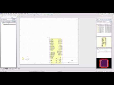
The schematic editor is the workspace where you can design and edit circuits in EasyEDA. To create a new schematic, click on the “New Schematic” icon on the left toolbar.

This will open up a blank schematic sheet with the toolbar on the left side.

The schematic editor toolbar contains all the functions you need to create your circuit diagram:

  • Components: Add components like resistors, capacitors, transistors etc. from the component library.
  • Wires: Draw connecting wires between components.
  • Text: Add text labels, notes and titles.
  • Annotations: Add input/output pins, power symbols, no connect symbols etc.
  • Tools: Advanced tools like bus, wire label, global label etc.

To place components, click the Components button and you will see the component library window open up. Browse or search for the part you need and click on it to add it to the schematic.

You can press the Escape key or click on the background to stop placing components. Use the Wires tool to connect components together.

Here is simple schematic example with a 555 timer circuit:

The schematic editor has all the features you would expect like copy/paste, undo/redo, delete, selection tool etc. Right click on components and wires to access these functions.

Once your schematic is complete, you can switch to the PCB editor to design the printed circuit board.

Creating PCB Layouts

To create the PCB layout for your schematic, click on the “Convert Project to PCB” icon in the toolbar.

This will open up the PCB editor and automatically import all the connections from your schematic.

The PCB editor works similarly to the schematic tool. All the footprint libraries, design functions and features are located in the left toolbar.

  • Footprints: Add footprints for components from the library.
  • Tracks: Draw copper tracks to route connections.
  • Text: Add text labels, values, info etc.
  • Dimensions: Add dimension lines, markers etc.
  • Shapes: Draw mechanical outlines, mounting holes etc.
  • Tools: Advanced PCB editing tools.

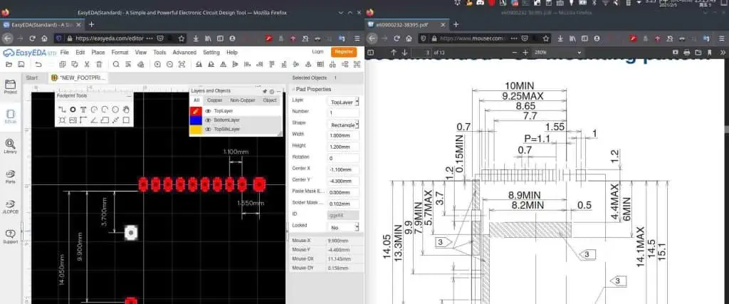
To place footprints, select the footprint you need from the component library window. Rotate and move the footprints to match the schematic layout.

Use the Tracks tool to connect the component pads together with copper tracks. You can set the track width and change layers while routing.

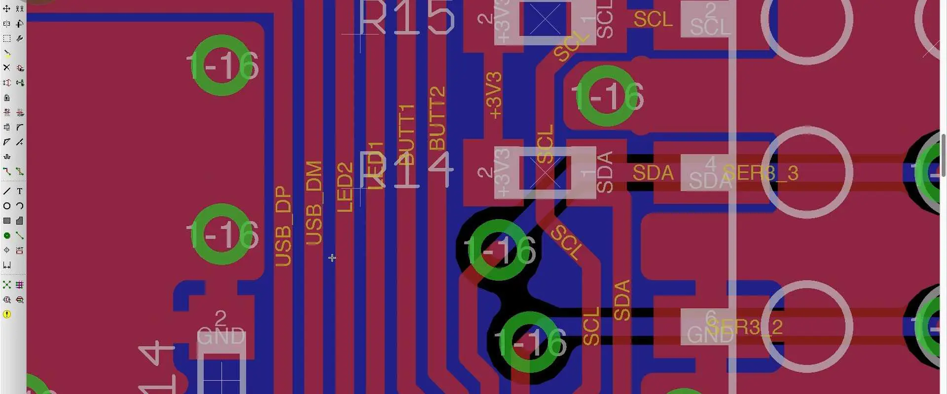
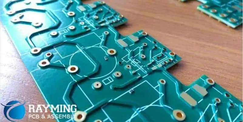
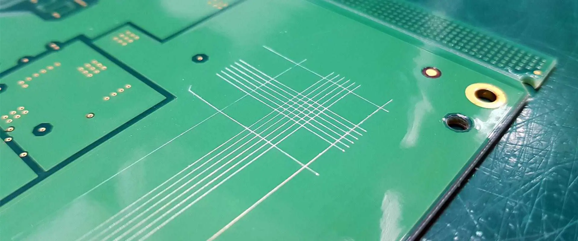
Here is an example PCB layout:

The auto router can be used to automatically route all connections. But it is recommended to manually route critical tracks for optimal layout.

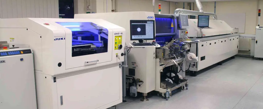
Once the PCB layout is complete, you can generate fabrication files and get PCB manufacturing quotes directly within EasyEDA.

Circuit Simulation with NgSpice

PCB Antenna Layout
PCB Antenna Layout

EasyEDA integrates the open source NgSpice simulator which allows you to simulate and analyze circuits right inside the tool.

To simulate a schematic, click on the “Simulate” icon on the toolbar.

This will bring up the simulation dock on the right side with schematic symbol pins and simulation settings.

Select the input and output pins, set simulation parameters and click Run to simulate the circuit. You will see the output waveform displayed instantly.

Here is an example simulation result for a simple BJT amplifier circuit:

NgSpice is a powerful analog circuit simulator that allows you to do DC, AC, transient analysis and more. You can probe signals, run parametric simulations and even perform digital logic simulations.

Being able to simulate and verify circuits before ordering PCBs helps avoid errors and saves a lot of prototyping time and effort.

Generating Gerber Files

Once your PCB design is complete, you can generate the Gerber files required for fabrication directly within EasyEDA.

Click on the “Generate Fabrication File” icon in the PCB editor toolbar.

In the dialog box, select the PCB color, thickness and layers required. Make sure to check “Include Drills” option. Then click Generate.

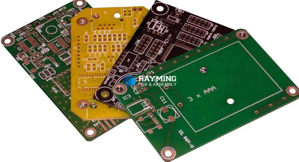
This will generate a zip file with all the Gerber and drill files needed to fabricate your PCB design. The zip file contains:

  • Top, Bottom, Inner copper layers
  • Silkscreen layers
  • Solder mask layers
  • Drill files
  • Board outline file
  • Position (centroid) file

You can save the zip file and upload it to any PCB manufacturer for fabrication.

Ordering PCBs from JLCPCB

One of the best features of EasyEDA is the ability to instantly order custom PCBs from JLCPCB right from within the tool itself.

JLCPCB is one of the most popular and affordable PCB manufacturers, especially well known for their SMT assembly service.

To order PCBs, click on the “Generate Fabrication File” icon first to generate the Gerber zip file.

Next click the “Order at JLCPCB” button and you will see the Order page load up with your design ready for purchase!

JLCPCB offers a wide range of PCB options to choose from including:

  • Number of PCBs needed
  • Different materials like FR4, Rogers, Flex PCBs etc.
  • PCB thickness
  • PCB color
  • Copper thickness
  • Via process
  • Lead time
  • Special requirements like impedance control or HAL

You can select the options as per your requirements and you will get the instand fabrication quote on your screen.

Once you are satisfied with the options, you can go ahead and place the order! The PCBs will get manufactured at JLCPCB and shipped directly to you in a few days.

This seamless integration with JLCPCB ordering makes prototype PCB fabrication super quick and easy. You can go from design to PCBs in hand in less than a week!

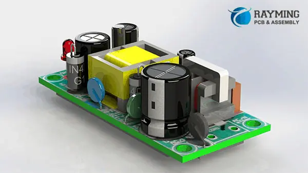
EasyEDA PCB Assembly

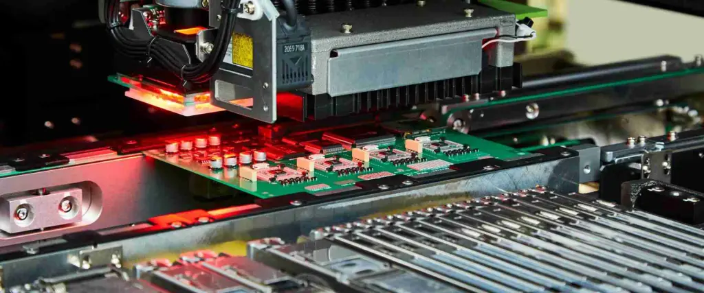
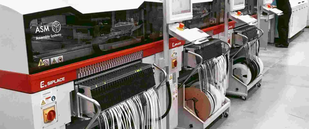
In addition to PCB fabrication, EasyEDA also allows you to easily order assembled PCBs from JLCPCB through their SMT Assembly service.

To order assembled PCBs, click on the “Order at JLCPCB” button and check the “SMT Assembly” option:

You can upload your component BOM file and JLCPCB will handle the entire PCB assembly process including:

The assembled PCBs will be shipped to you fully tested and working, ready for your project.

This end-to-end electronics manufacturing service makes EasyEDA a very powerful prototyping tool.

EasyEDA Open Source Model

One of the nice things about EasyEDA is that it is completely open source!

The full source code for EasyEDA is hosted on GitHub at https://github.com/easyeda and published under GPL v3.0 and LGPL v2.1 licenses.

Anyone can download the code, contribute to the project and self host their own EasyEDA server if needed.

The open source model has helped build an active community around EasyEDA development and new features. Users can provide feedback, raise issues and even directly contribute code to add enhancements.

For makers and engineers who value open tools, EasyEDA is an excellent open source EDA platform.

EasyEDA Community and Support

As an open source project, EasyEDA has benefited from an engaged community of users and contributors.

The main discussion forum is available at https://easyeda.com/forum. You can find thousands of posts on various topics like software help, electronics design advice, PCB reviews and announcements.

It’s a great place to get any EasyEDA related questions answered or just participate in community discussions.

There is also documentation available at docs.easyeda.com that covers the basics of using EasyEDA for beginners.

For additional help, you can contact EasyEDA support through the Support Page. The team is very responsive to user questions.

The active forums, documentation and helpful support staff make EasyEDA an ideal tool for learning PCB design.

Conclusion

EasyEDA provides a full suite of EDA tools for circuit design, PCB layout, circuit simulation and manufacturing – all available for free online.

Some of the key benefits of EasyEDA:

  • Intuitive and easy to use schematic and PCB editors
  • Comprehensive component libraries with 500k+ parts
  • Integrated NgSpice simulator for circuit simulation
  • Open source software with active community support
  • Seamless PCB manufacturing through JLCPCB integration
  • End-to-end PCB assembly service available

With its combination of excellent features, convenient online access, open source model and great community support, EasyEDA delivers an unmatched electronics design experience.

Both beginners and experienced engineers can benefit from using EasyEDA for their projects and enjoy the process of going from design idea to finished PCB product.

Hopefully this tutorial gave you a good overview of getting started with EasyEDA. Try it out today and experience the convenience of browser based PCB design!

Frequently Asked Questions

Here are some common FAQs about EasyEDA:

1. Is EasyEDA really free to use?

Yes, EasyEDA is completely free to use for schematic design, PCB layout, circuit simulation and even generating fabrication files. You can use it without any restrictions in your browser.

The only payment needed is when you actually order manufactured PCBs from JLCPCB through the EasyEDA integration. But the tool itself does not cost anything.

2. What are the layers supported in EasyEDA?

The PCB Editor supports up to 2 copper layers, along with silkscreen, soldermask, outline, drill layers etc. So you can design simple dual layer boards well suited for hobby and prototype use.

For more complex multi-layer boards, other paid EDA tools will be required. But EasyEDA works very well for basic 2 layer boards.

3. Can I export designs from EasyEDA?

Yes, EasyEDA allows export to common file formats:

  • Schematics can be exported to PNG, JPG, PDF and netlist files.
  • PCB Layouts can be exported to PNG, JPG, Gerber RS-274X, DXF, BOM files etc.

This allows you to use the designs outside EasyEDA if required.

4. Does EasyEDA offer version control or collaboration features?

Currently there is no built-in version control or collaborative editing in EasyEDA. The designs are saved in your personal account workspace.

But since it is open source, developers could potentially contribute plugins to enable Git version control integration in the future.

5. How is EasyEDA licensed?

The EasyEDA source code is licensed under GPL v3.0 for maximum open source freedom. This means you are free to even create commercial closed source derivatives.

The digital content like component libraries use the more restrictive LGPL v2.1 license. This ensures the libraries remain open.

So in summary, EasyEDA provides very liberal licensing for full OSS benefits.

More Facts on EasyEDA PCB

When it comes to designing, you need the right tool. Nobody wants to encounter difficulty while designing for clients. The issue is mostly with getting the right software application or tool for designing. If you want to use an easy online design tool, what comes to your mind? For project management, graphic design, architectural designs, and town planning, you need a strong and powerful PCB drawing, design, and development tool.

You don’t have to bother any longer if you are facing challenges with your design. All you need is an EasyEDA tool. This tool is essential for your design and is quite accessible. If you are skeptical about becoming a pro at designing, it is because you do not have an EasyEDA tool. This article shall address everything you need to know about this circuit simulator. If your question is: “Does EasyEDA help with design effectively?” Yes, it does. Interestingly, it is not just for any type of design.

What Does EasyEDA Do?

EasyEDA is a tool that helps with designing. This tool is specifically designed for engineers, architects, and everyone working in the field of designs. This tool runs on the web and is backed up by EDA. The EasyEDA tool guarantees hardware engineer effective designs.

What is an EDA?

In case you are wondering what an EDA is, let us get to explain what it means. EDA stands for Electronic Design Automation. This tool aids design on the computer or any system. An EDA has to do with a group of some software or programming tool that aids or maintains every other application. The EDA helps in designing any kind of integrated circuit which is in relation to an electronic system. Not only is it used for integrated circuits, but it can also be used for PCB designs. In a nutshell, an EDA is a designing tool.

Having understood what an EDA means, it is paramount to discuss more on EasyEDA. EasyEDA is a web running tool that helps any engineer to simulate schematics without restrictions. Engineers work on the electrical diagram. With EasyEDA, the circuit diagram can reveal the real connections in the electrical design of any work. The circuit diagram basically is used for any PCB layout. This implies that for your PCB layout, the EasyEDA makes your design faster and easier.

More Facts On EasyEDA

EasyEDA tutorial

While you get to know the capability of this tool, also note that it is available in various languages. This will aid better results. EasyEDA tool is available in German, Japanese, French, Polish, Spanish, Portuguese, Swedish, Russian, and English among other languages.

This is an EDA software that helps with creating any schematic image or diagram. That is why hardware engineers mostly use it. Not only does it allow you to create diagrams, but it also enables its editing. This in a way makes the work less cumbersome. It could also help in the innovative creation of any kind of billing materials. It is essential for some important outputs you find in PNG formats.

EasyEDA has digital platforms such as Windows, macOS, and Linux where it runs or operates maximally. It is noteworthy that this is commercial software. It is very good for any kind of schematic capture. It aids the circuit diagram to become better with the PCB design.

This tool has a lot of amazing features. These features help its running on the web. This is a form of an integrated web tool that works with SPICE stimulation of any circuit.

Features Of EasyEDA Tool

SPICE library: Out of its numerous features, the EasyEDA has a SPICE library that expands. The model library has the capability to become large in its scope. It has about 10,000 libraries for the public. Among the public libraries are the footprint and symbol libraries. It also has the footprint edit.

Drawing Capabilities: This tool is a designing one. Not only is it good for designing. It also has drawing capabilities. This comes in a very easy, smooth, accessible, friendly, and simple way. It is a very powerful tool for general and automatic drawing capabilities.

Script Support: This is one of the amazing features of this tool. EasyEDA provides everyone with a script support mechanism.

Reliability: Everyone wants a truly reliable tool. You do not want a situation where you get stuck on the web. This tool has the capability to work anywhere. That makes its accessibility top-notch. Not only does it work anywhere, it also works anytime. It is not a tool that stops working at a particular period of the day.

Schematic Capture: It is important to elaborately discuss more on this. This tool has a schematic module with SPICE models that run effectively. It has the Netlist export for Pads, Spice, FreePCB, and others. Also, it has the capacity for documentation export such as SVG, PDF, and PNG at all times. It has BOM export capability too. It has a photo view, 3D view, Auto Router, and documents recovery memory.

Other features of this tool are; PCB fabrication, purchase chain for various components, API provision, and DRC which is for the design rules.

Designing With EasyEDA Tool Explained

EasyEDA Software is very important for every budding designer. Engineers know the importance of using this tool. This tool comes with a simple sketching panel. It saves a lot of time because of the naming quality system it possesses. You can design any PCB with the aid of the EasyEDA tool.

While designing, you can click on the new schematic. However, before that, you must have clicked on the new project file. There is always a connection with the component in each image. While the design progresses, it is paramount to organize the components.

You organize each component as influenced by the available image. Ratsnest is what the blue lines are referred to. The Auto Router helps you to check the image during your design process. You also ensure you save the fabrication output during your design. Also, remember to download and save your Gerber documents. Afterwards share it on the fabricator.

More On EasyEDA – What You Probably Haven’t Heard Before

EasyEDA is a very good tool for PCB design. This free tool gives all users some unique experience that makes them enjoy the act of designing. EasyEDA Online tool is being updated daily and it keeps getting better for users.

EasyEDA Tutorial is available in PDF format for every learner of design techniques. Interestingly, the version is simple to comprehend. There is a free membership available for the public. This is garnered towards learning. The moment one registers, there’s room for downloading the Gerber documents. The files do not attract any charges. Optionally, some printable PCB design diagrams are available in either PDF or PNG formats. One can both publicly and privately share PCB designs. For the simulations, it involves the application of the conceptual model. This tool aids learning ability in people to understand what model the simulation represents.

One can also import libraries. This helps with the designs. One thing is that EasyEDA helps with direct links that take you to not less than 100,000 real-time features available at the LCSC. The team collaboration of this tool is also great. One can create some spice simulations backed up by the circuit.

Frequently Asked Questions

Who Are Those Who Can Access EasyEDA?

Some are of the opinion that only specific professionals can use this tool. That is not the case. As long as you are enthusiastic about learning design, you can use this tool to your advantage. It is an EDA tool for hardware engineers ( they use it mostly), designers, interior designers, graphic designers, teachers, parents, filmmakers, 3D enthusiasts, students, and media practitioners.

Do I Need To Install My Software Application Before Usage?

Some people cannot use this tool without installing any kind of software. The good thing is that you do not have to necessarily install any kind of software before you can use this tool. Basically, all you need for the effectiveness of the tool is to open an EasyEDA in your available HTML5 powerful browser. It must be a supported browser for it to run well.

Is EasyEDA Free?

Many people are skeptical that a tool like EasyEDA could be free. The fact is the developers have made provision for the free usage of the tool. The notable features of this tool can be accessed by everyone free of charge. However, there is room for payment of subscriptions to EasyEDA. This is based on a monthly basis.

Conclusion

The EasyEDA tool is simple to use. It is a free tool that helps your design come out successfully. With the circuit design, you can have any design of your choice. It is also important to keep using the tool till you have gained mastery of it. Users should note that there is a daily update on the Easy EDA Software. This is to help the tool work better and become advanced. Getting a tutorial will accelerate your learning. EasyEDA tool is also for children because it has the basics tools for them.

What is The lastest Surface Mount Technology ?

Surface Mount Technology

Introduction

Surface mount technology (SMT) refers to the method of mounting electronic components directly onto the surface of printed circuit boards (PCBs) without through-hole connectors. Originally developed in the 1960s, SMT has now become the standard method of assembling modern PCBs across consumer, industrial, automotive, telecom, and military electronics.

This comprehensive guide covers everything related to SMT including:

  • The history of surface mount assembly
  • Benefits compared to through-hole mounting
  • Description of common SMT components
  • SMT soldering and attachment methods
  • Typical SMT assembly process steps
  • SMT equipment for fabrication, printing, placement, reflow
  • Quality control and yield best practices
  • Environmental considerations for lead-free assembly
  • Latest innovations advancing SMT technology

Letโ€™s take a detailed look at what surface mount technology entails and how it has revolutionized electronics manufacturing.

History of Surface Mount Technology

Surface Mount Technology

Surface mount technology evolved from earlier hybrid assembly approaches combining surface mounted and through-hole components:

1960s – Components glue-bonded onto PCB surface

1970s – Tape automated bonding (TAB) for ICs

1980s – Adoption of standard gull-wing SMT components

1990s – High speed SMT pick-and-place and reflow equipment

2000s – Lead-free manufacturing and micro-SMT advances

2010s – 01005 passives, microBGA, PoP, flip-chip, high-density SMT

Thanks to continuing innovations, SMT now supports ultra-miniature components for highly automated assembly, driving electronics product performance, size, and cost improvements.

Benefits of SMT

Compared to through-hole PCB assembly, surface mounting offers numerous advantages:

  • Smaller components and closer spacing enables miniaturization
  • Higher component density allows more functionality per PCB area
  • Simpler board layouts reduce layers and vias
  • Easier automation with faster component placement
  • Eliminates tedious lead clinching and trimming
  • Cost-effective volume manufacturing
  • Lead-free assembly improves environmental friendliness
  • Better electrical performance from reduced parasitics

Thanks to these benefits, SMT has largely replaced through-hole mounting as the standard assembly technique for high-volume production. Next weโ€™ll examine common component packages designed for SMT.

Surface Mount Component Packages

A range of standardized component packages have been developed optimized for surface mount assembly. Some popular examples include:

Quad Flat Packages (QFP)

  • Square ICs with leads extending from four sides
  • Pins underneath spaced on 0.5mm grid typically
  • Available in various sizes from 20 pins to over 200 pins
  • Allowing effective washing during assembly

Ball Grid Arrays (BGA)

  • ICs with input/output terminations in grid array of solder balls on bottom
  • Allows high density component mounting without perimeter leads
  • Larger pitch balls used for mechanical support; finer pitch for I/O
  • Advanced variants like PBGA, CBGA, EBGA, etc.

Chip Scale Packaging (CSP)

  • IC packages size nearly identical to silicon chip dimensions
  • Very compact with fine lead spacing
  • Allows maximizing PCB area utilization
  • PoP, fan-out wafer level, and other CSP configurations

Land Grid Arrays (LGA)

  • Input/output pads in grid pattern on underside of component
  • Mated with corresponding pads on PCB through compression
  • Enables contacts across entire package underside for very high I/O density
  • Common for large FPGAs, GPUs, and other complex devices

Passives

  • Rectangular chip resistors, capacitors, inductors, etc.
  • Available in sizes including 0201, 0402, 0603, 0805, 1206, etc.
  • Metric codes denote size (e.g. 1201 is 0.6mm x 0.3mm approx)

Continuing technology improvements allow steadily shrinking component sizes while increasing available I/O density. This drives electronics innovation and new product capabilities.

SMT Attachment Methods

SMT soldering Process

With no leads to insert, surface mount components are attached to pads on the PCB through methods including:

Soldering

  • By far the most common attachment approach
  • Provides both electrical connection and mechanical bond
  • Reflow or wave soldering used depending on package style

Conductive Adhesives

  • Silver epoxy glues conduct electricity for connection
  • Provides higher resistance and lower mechanical strength than solder
  • Limitations on temperature during curing

Press-Fit Connections

  • Spring-loaded pins compressed into plated through holes
  • Gas-tight, reworkable connection without solder
  • Requires precise hole machining and pad oxide cleaning

Sockets

  • Intermediate socket soldered to board mates with pins of package
  • Allows easy replacement of components like CPUs for upgrades
  • Higher cost, contact resistance, and poorer thermal performance

Among these options, soldering remains the optimal choice for most components due to superior electrical, thermal, and mechanical characteristics.

SMT Soldering Processes

Attachment of surface mount components is typically achieved using either of two primary soldering processes:

Reflow Soldering

  • Solder paste applied to pads via stencil/screen printing
  • Components placed onto paste deposits
  • Entire assembly heated in oven profile above solder melting point
  • Solder reflows wetting pads to form solder joints

Wave Soldering

  • Bottom side passed over flowing wave of molten solder
  • Solder adheres to exposed pads to form solder joints
  • Top already assembled separately with adhesive or reflow
  • Limited to durable components able to withstand wave exposure

The assembly side used depends on the package style. Sensitive small components use reflow while connectors and some passives are wave soldered.

SMT Assembly Process Overview

A typical complete surface mount assembly sequence consists of the following steps:

1. Solder Paste Printing

Solder paste containing powdered solder and flux is applied to pads through a stencil.

2. SMT Component Placement

Components are precisely picked from feeders and positioned onto pads using automated pick-and-place machines.

3. Reflow Soldering

A controlled thermal reflow profile melts the solder paste deposits to wet pads and form solder joints.

4. Through-Hole Component Insertion

Any through-hole components are inserted either manually or with automated inserters.

5. Wave Soldering

The bottom side goes through a solder wave to attach remaining components.

6. Cleaning/Finishing

Excess fluxes are removed using cleaning processes. Final finishes or coats are applied.

7. Inspection/Test

Automated optical inspection and electrical testing validate assembly quality and function.

8. Conformal Coating

A protective conformal coating may be applied to shield components.

Highly optimized implementation of these process steps allows efficient, high-yield assembly of quality boards. Next letโ€™s look closer at some of the key surface mount technologies and equipment used.

Solder Paste Printing Equipment

SMT Lines

Solder paste application tools include:

Stencils

  • Laser cut metal foils 0.1-0.15mm thick
  • Stencil apertures align with PCB pad positions
  • Allows rapid dispensing of precise paste volumes

Solder Screens

  • Steel or polyester fine mesh screen stretches on frame
  • Best for high-volume production with repeating designs
  • Allows higher height tolerance

Printers

  • Automated machines align stencil and print solder paste
  • Prints can print ~15 cm^2/sec at 150 ฮผm feature size
  • Provides consistent, high-speed, high-precision paste dispensing

With high quality stencils, precision printers, and well-tuned processes, printing delivers paste deposits with tight process margins supporting advanced assembly.

SMT Component Placement Systems

Automated pick-and-place systems position components for assembly. Key characteristics include:

  • Feeders – Tape, sticks, trays, etc. to supply components
  • Pick Heads – Nozzles for vacuum pick-up of components
  • Cameras – Pattern recognition for precise alignments
  • Work Holder – Moving PCB platform and clamping
  • Software – Programming component locations and sequences

High-end chip shooters provide fast, flexible, precision placement with advanced features like:

  • Feeder racks with hundreds of components
  • Dual gantry heads for simultaneous pickup/placement
  • Component flipping/rotation capabilities
  • Modular heads supporting various components
  • On-head barcode scanning for traceability

State-of-the-art pick-and-place systems can accurately assemble over 150,000 components per hour, enabling extremely high-volume production.

SMT Reflow Oven Options

Reflow ovens pass assembled boards through a controlled thermal profile to reflow (melt) solder paste and form solder joints. Types include:

Convection Ovens

  • Use fans to circulate hot forced air
  • Provides good heat transfer efficiency
  • Challenging to evenly heat large boards

Vapor Phase Ovens

  • Use evaporating solvent to uniformly heat PCB
  • Excellent thermal uniformity
  • Condensation/cleaning considerations

Infrared Ovens

  • Use IR lamps or panels to heat boards
  • Very fast response time
  • Can be difficult to evenly heat all areas

Laser Soldering

  • Directed laser energy to melt solder joints
  • Minimal thermal impact on rest of assembly
  • Typically used for small rework applications

Modern ovens with multiple controllable heating zones provide the thermal precision needed for lead-free solders and advanced packages.

SMT Inspection Systems

Consumer Electronics Assembly

Automated inspection validates assembly quality:

2D AOI

  • 2D machine vision inspection of joints, parts, defects
  • High-speed image matching algorithms
  • Limited ability to detect misplaced bottom-side parts

3D AOI

  • Laser profiling and scanning to obtain 3D surface data
  • Detects lifted leads, skewed parts, and solder defects
  • Significantly higher sensitivity than 2D AOI

AXI

  • Automated x-ray inspection
  • Sees inside components and connections in 3D
  • Detects defects like voids, lack of wetting, etc.
  • Complementary technique to optical AOI

These automated optical and x-ray tools replace tedious manual inspection with comprehensive analysis for process feedback and quality control.

Lead-Free SMT Assembly

Growing environmental concerns led the industry shift from tin-lead solders to lead-free alloys like SAC 305 (SnAgCu). Key considerations:

  • Higher soldering temperatures required
  • More susceptible to defects like head-in-pillow
  • Components and boards must withstand higher temps
  • Solder baths converted to lead-free
  • Process tuning for optimal wetting and joints

Despite challenges, rigorous process controls allow assembling lead-free electronics reliably.

Latest SMT Innovations

Ongoing technology developments continue advancing SMT capabilities:

  • Micro SMT – Enabling 0201 passives, microBGAs, wafer level packages, and beyond
  • 3D Packaging – Alternatives to larger chips like SiP and PoP
  • ** additive processes** – Inkjet solder printing, aerosol jetting, ultimately pick-and-place at chip scale
  • Smart Data – Analytics and machine learning for process optimization
  • Direct Integration – Flip-chip and other direct on-substrate approaches
  • Flexible Hybrid Electronics – Printing electronics onto flexible substrates

These innovations will allow packing greater functionality into smaller and smaller electronic assemblies.

Conclusion

This guide provided a comprehensive overview of surface mount technology, the transformational manufacturing approach that has enabled electronics to become ubiquitous across all areas of life today.

We traced SMTโ€™s origins in the 1960s to present-day automated factories assembling miniature components at remarkable speeds and volumes. The benefits over through-hole assembly are clear in terms of size, performance, cost, and manufacturability.

Understanding SMT provides key insight into the production processes, components, equipment, inspection methods, and innovations that allow translating circuit board designs into functioning devices. Mastering SMT fundamentals is therefore critical knowledge for electrical engineers and professionals across the electronics industry.

The next wave of SMT breakthroughs in areas like additive manufacturing and 3D integration will continue driving electronics advancement into coming decades. By leveraging these manufacturing capabilities, engineers can turn visions into reality.

Frequently Asked Questions

What are common SMT assembly defects?

Typical SMT defects include missing components, skewed/misaligned parts, insufficient solder, excess solder, solder balls/bridges, thermal damage, tombstoning, cuts/nicks, and holes/voids in joints.

What types of solder alloys are used in SMT?

Common solder pastes are SAC 305 (3% silver, 0.5% copper) and SAC 105 (lower silver). Other alloys include SnCu, SnAg, and SnZn. Lead-free solders require higher melting temperatures than tin-lead.

How small can SMT components be made?

0201 chip components measuring just 0.25mm x 0.125mm are common. New techniques allow soldering chips down to 0.15mm size. The lower limit is still advancing through micro-assembly breakthroughs.

What causes tombstoning defects in SMT?

Insufficient solder volume and surface tension imbalances during reflow can lift smaller components up on one end like a tombstone. Adjusting paste deposits, profiles, and layout helps prevent.

How does SMT affect thermal management?

The move to SMT helps by eliminating through-hole lead thermal resistance. But high density SMT heightens the need for thermal vias, internal layers, and airflow to prevent excessive component temperatures.

Conclusion

From its origins decades ago, surface mount technology has revolutionized electronics manufacturing and enabled steady improvements in capabilities, size, functionality, speed, and cost. Mastering SMT principles provides invaluable insight into the foundation underpinning electronics assembly and innovation.

The Go-To Guide on Buying PCB

buying pcb

Printed circuit boards prove pivotal to the functioning of any electronic device. It can include your digital watch, smartphone, or large and complex industrial electronic devices. A PCB helps a device’s components communicate through electronic and electrical signals to serve their intended purpose. But regardless of the type of device, information on the type, make, and functionality of a PCB becomes instrumental in informing your purchasing choices. Otherwise, you can end up buying the wrong printed circuit board.

Are you an electronics enthusiast interested in buying PCB elements? Well, you might think that you have it figured out until you get to the market. But, unfortunately, PCBs can confuse you, especially when it comes to the right fit for your intended function. Therefore, the best buy PCB needs to have the crucial components and prove equally suitable to the intended device’s purpose. So what goes into shopping for a suitable printed circuit board?

Buying a Printed Circuit Board

Sometimes, the best way to shop for a PCB entails first understanding the type of PCB you want before shopping. Different types of PCBs exist, and each has its advantages when it comes to usage. For instance, an Eagle PCB can prove markedly from a Breadboard PCB. Secondly, you need to know the best place to get such a printed circuit board. Plenty of organizations produce PCBs with fluctuating quality, customization options, and prices. Therefore, you have to understand the available options, pricing, and other aftersales activities to get the best buying PCB experience. Finally, you have to understand the avenues available to you regarding the PCB ordering process. Companies differ in their approaches as some prefer you to order PCB online while others have alternative in-person arrangements.

Considerations to Make While Buying PCB

Buy PCB Board
  • Suitability of the PCB to your circuit needs
  • You will be amazed by the numerous PCB types available in the market. PCB types include the single-layer PCB, double-layer PCB, multi-layer PCB, rigid PCB, flexible PCB, and rigid-flex PCB. Therefore, if you aim to use your PCB order for industrial, medical, aerospace applications, then a multi-layer PCB might prove more suitable. For other uses such as cameras, calculators, etc., a single-layer PCB can suffice. Additionally, the technology used to manufacture these printed circuit boards also differ, and you have a likelihood of finding them with names such as Eagle, Kicard, etc. It becomes instrumental that in such situations, you do not get confused. Further, for testing and troubleshooting purposes, you should buy a breadboard PCB.

The bottom line for all this entails knowing all the available PBCs and what type suits your intended application the best before buying.

  • Pricing of the printed circuit boards
  • Make a decision to buy PCB board based on the pricing of that specific board. It can include a single-layer, multi-layer, or double-layer. Please note that all PCB products or services providing companies such as the RayMing PCB and Assembly use a cost-related model to attach price tags on diverse PCB products. For instance, a multi-layer printed circuit will cost more than a double-layer and single-layer PCB due to the technicality involved in the manufacturing process and more materials for the components. Additionally, companies charge more when it comes to customization services. Therefore you will have to use more money to buy these PCBs that align with your specific and unique attributes.
  • Manufacturing company. Plenty of companies produce printed circuit boards, but the quality and type of service differ from one company to the other. For example, some companies will provide manufacturing, fabrication, and assembly services, while some can only fabricate and assemble. Therefore, it becomes crucial to canvass and find the best company that will provide the required PCB at an affordable price and quality and excellent customer care service. The type of company and their product distribution services will also impact whether you can conveniently buy from them or not. For instance, if a company only provides PCB products within a specific territory or if it can allow you to place an order and buy online, complete with shipping services. Therefore, examine this crucial factor when buying a PCB to reduce potential disappointments.

Additionally, can the company produce your customized PCB design? The company you opt to procure a PCB from should have the capacity to customize the unique features you want to incorporate into your printed circuit board.

How to Order for Printed Circuit Board

Once you figure out what kind of printed circuit board you want and consider earlier stipulated, it becomes instrumental in placing an order of the PCB from your preferred PCB Company. But, before you order, try and gauge whether the manufacturing company you have settled on only produces standard sizes or short runs as well. It will assist you in buying an inexpensive set without any need to pay upfront for a large custom PCB batch, especially when you only want a single or two pieces.  

Steps.

  • Develop a circuit schematic and design. The two components become crucial for any printed circuit board, as you would not require a PCB board without a circuit. A variety of tools exist that you can use in creating a schematic. However, use a tool that will not only allow you to simulate the circuit’s behavior but test it as well. It should also allow you to develop at least a single working prototype and ensure functionality as designed before making the order.
  • Design your PCB. It is the next step after making the schematic and can prove tasking and a bit time-consuming. Here, you must demonstrate the technical know-how to route the tracks and how their outlay affects your circuitโ€™s performance. However, provided it’s a simple one for the initial circuit, the process can become less tasking. In addition, a lot of manufacturers have specific design software solutions for your use in this process. Thus, it becomes critical to search for these, complete with instructions on using them in their respective websites.

Additionally, note that you will have to set your project dimensions based on the customary sized board the company offers, as you will likely get these from your order. Otherwise, the manufacturer may decline to build your PCB at the specified price.

An excellent benefit of using such design software entails the standardization of the output files into the Gerber format. It is a file format that gets used for plotters when the actual track-printing occurs on the board. Therefore, any tool you choose to deploy needs to have the export option that will allow you to export your design in the Gerber format.

  • Double-check your design. Cross-checking and ensuring everything is in order becomes critical at this stage. Therefore, ensure the prototype, design, and board layout have no mistakes to avoid the costly replacement, especially after procurement of the boards. Once you have ascertained that everything is in order, you can upload the Gerber files, pick the board you want, and pay.
  • Once you receive the board from the manufacturer, check for any shipping damage and manufacturing defects like broken boards, defective and incomplete tracks, and undrilled holes. The process becomes vital before embarking on the soldering process of parts. It will allow you to replace parts quickly if you spot defects besides saving your costs on the replacement parts.

How Printed Circuit Board Get Priced

rogers substrate

PCBs have a diverse range of reliability, complexity, price, and quality points. However, the typical circuit board can cost as low as fifty cents to about three hundred dollars based on your requirements. But the cost of PCB gets influenced by many factors, including the following.

  • Assembly type. The type of assembly can drive the cost of a printed circuit board up or down. For instance, SMA, which entails assembling components on the surface, proves less expensive and with a faster manufacturing process compared to through-hole soldering. However, the latter has a sturdier connection concerning components than the latter. It thus proves the preferred tech by many, despite its steep price.
  • Component placement. The components placement within the board can increase or reduce the PCB price. Therefore, re-evaluate how you want them placed to reduce the manufacturing price.
  • The components number. The number of components within your circuit board will impact its price. It is because it arises from the procurement of these parts besides the cost of manufacturing. Therefore, try hard to ensure that your circuit proves as efficient as possible to reduce the PCB price.
  • Component’s package size. Industry size component package sizes lead to more affordable PCBs. Therefore, try and ensure you stick to these.
  • Component package besides the required process
  • Every component package needs to get attached using a particular process. Therefore, whenever you opt for delicate, complicated, and hefty component packages, the price also increases.  
  • Batch size and quantity. The number of PCBs you order besides the batch size will influence the overall cost of the PCB. Larger quantities of PCB fetch a lesser cost compared to smaller quantities. However, the batch size also dives the cost, something that gets overlooked often. Therefore, consult with your PCB manufacturer to understand what works best and will cost less.
  • Special component or parts preparation needs can also increase the cost of PCB. Therefore, if you can, use standard processing and size requirements.
  • Coating, potting, material and layers, and BoM also influence the cost of PCB; therefore, pick options that can reduce the cost of PCB.

How much does it cost to buy a PCB?

Introduction

Printed circuit boards (PCBs) provide the foundation for almost every electronic device. But what factors determine the cost of procuring custom PCBs?

This comprehensive guide examines the key considerations impacting PCB pricing including design complexity, board materials, manufacturing volumes, lead times, testing requirements, and more.

By understanding the drivers of PCB costs, electrical engineers can budget appropriately and make informed design tradeoffs. Weโ€™ll provide example quotes across hobbyist, prototype, and production scenarios to illustrate how widely prices can vary depending on application requirements.

Letโ€™s dive in to understand what makes some PCBs cheap while others become quite costly!

PCB Cost Dependencies

Below are some of the main factors that influence the pricing when sourcing custom PCB manufacturing:

Manufacturing Volume – Small prototyping quantities cost much more per board than high-volume production runs.

Board Size – Larger boards require more materials and cost more than smaller boards.

Layer Count – Base 2-layer boards are cheaper; each additional layer adds expense.

Board Thickness – Thinner PCBs use less material than thicker boards.

Board Shape – Rectangular boards are most cost effective. Irregular board outlines increase cost.

Materials – FR-4 glass epoxy is standard. Higher performance materials cost more.

Trace/Space – Tighter trace spacing and thinner traces increase fabrication difficulty and price.

Finishes – Immersion silver or gold cost more than standard HASL, OSP or ENIG.

Coatings – Conformal coatings add additional process steps and cost.

Hole Sizes/Counts – Many small holes and vias increase drilling time and tooling complexity versus fewer large holes.

Tolerances – Tighter fabrication and assembly tolerances require more attention and expense to fulfill.

Testing – Electrical testing, AOI inspection, x-rays, and other testing add cost but reduce escapes.

Lead Time – Faster turnaround requirements may command a premium to expedite the order.

Order Quantity – Due to setup costs, ordering many small panels costs more than fewer large panel batches.

Location – Local vs. overseas manufacturing involves tradeoffs of cost, lead time, communication, quality, and IP risk.

Weโ€™ll now explore how these factors contribute to overall board fabrication and assembly pricing across various use cases.

PCB Cost Case Studies

bare PCB layout design to cut cost

To better understand how the dependencies above impact cost, letโ€™s look at PCB price examples for hobbyist, prototype, mid-volume, and high-volume production scenarios:

Hobbyist PCB Costs

For hobby designers making boards at home in very low quantities, costs may be as little as $5-$10 per board in single unit batches.

Key characteristics:

  • Typically 2 layer FR-4 boards under 50mm x 50mm in size
  • Limited number of large through-hole parts
  • Traces and spacing around 8-10 mil resolution
  • Simple rectangular board outlines
  • Purple PLA solder mask and silkscreen
  • No special films or finishes beyond basic tin-lead HASL
  • Panels supplied to hobbyist shops like OSH Park, JLCPCB, PCBWay, etc.

At these vendors, customers upload Gerber design files which get panelized and batch processed together to amortize setup costs. The turnaround time is typically 1-2 weeks.

For hobbyists, attributes like lead time, minimum order quantity, and convenience often take priority over lowest cost per board. But unit costs up to $10 are attainable.

Prototype PCB Costs

For professional engineers making 10-100 quantity prototypes in a lab, prices typically range from $50-$300 per board.

Characteristics include:

  • Often 4-6 layer designs up to 200mm x 200mm size
  • Higher mix of SMT and fine pitch components
  • Minimum trace/space around 4-5 mil with 6/6 mil being common
  • May require non-rectangular outlines, cutouts, etc.
  • Solder mask and silkscreen for branding
  • ENIG finish preferred for unassembled boards
  • Electrical testing
  • 2 week target turnaround time

In this range, full-service domestic or regional prototyping shops are best suited to provide quick-turn fabrication with testing and engineering support.

Medium Volume PCB Cost

For bridge manufacturing runs from 100-5000 boards, pricing averages $10-$50 per board.

Attributes include:

  • Often 4+ layers and may use thicker substrates
  • HDI technology with microvias
  • High mix of component types
  • 2-3 mil trace/space tolerances
  • Tight assembly tolerances required
  • Lead-free HASL or ENIG finish
  • UL mark requirements
  • Functional testing needed
  • 8 week acceptable lead time

Chinese manufacturers offer cost advantages at this volume through high automation, purchasing scale, and labor efficiencies.

High Volume Production PCB Cost

For mass production quantities above 5000 units, costs drop below $10 per board, sometimes below $1.

Characteristics:

  • High layer counts typical to maximize density
  • Fine line traces and spacing below 2 mil
  • demanding tolerances for auto assembly
  • Gold immersion finish
  • 100% automated optical inspection
  • Full functional circuit testing required
  • 12+ week production lead time acceptable

At this scale, overseas assembly allows drastic cost reduction through extreme economies of scale and highly mature automation.

As shown by these examples, PCB cost varies tremendously based on the design requirements, order quantities, lead times, and quality needs of the application. Let’s now examine the cost structure further.

PCB Cost Breakdown

PCB assembly cost breakdown

A PCB’s total price consists of a combination of direct fabrication costs, engineering support expenses, and profit margin for the manufacturer.

Direct Fabrication Costs

This includes the raw materials, labor, and equipment usage required to produce the boards:

  • Substrate laminates
  • Photoresists and chemicals
  • Copper and other metal platings
  • Tooling for processes like drilling
  • Machine depreciation
  • Operator labor for production steps
  • Overhead like facilities and utilities

More complex boards require more processing steps and expense.

Engineering and Support Costs

Additional services wrapped into board pricing often include:

  • Design for Manufacturing analysis and recommendations
  • Testing setup and program development
  • Quality assurance oversight
  • Prototyping and new product introduction
  • Quoting services
  • Project management and production engineering
  • Documentation and certification

These value-added elements increase with order complexity.

Profit Margin

On top of base costs, manufacturers typically apply a profit margin from 10-30%. More competitive pricing requires minimizing this margin.

By understanding the underlying cost structure, engineers can identify opportunities to reduce pricing through design modifications, vendor negotiation, or fabrication process improvements.

Optimizing PCB Cost During Design

Several design-stage choices influence PCB pricing. Below are techniques designers can apply to minimize fabrication and assembly costs:

  • Standardize on fewer board sizes and materials for volume aggregation
  • Minimize layer counts whenever feasible
  • Use smaller board sizes fitting within panel arrays
  • Reduce fine features like trace/space only where required
  • Standardize on common hole sizes to minimize tooling
  • Specify tolerances only where functionally required
  • Leverage prudent design rules avoiding unneeded complexity
  • Re-spin only for critical issues to avoid added iterations

While these guidelines help reduce cost, performance and reliability should not be sacrificed solely to lower price. Like any engineering decision, design tradeoffs should aim to balance technical needs and cost impacts.

Getting PCB Cost Estimates

When budgeting for a new board project, how can accurate cost estimates be obtained? Here are some tips:

Leverage Experience

Use intuition from past boards of similar specifications to gauge initial expectations for pricing.

Request Quotes

Reach out to potential manufacturers with key project details to receive formal quotations.

Use Cost Calculators

Many fabricators provide web forms allowing input of basic project parameters to estimate price ranges. These help set expectations.

Seek Manufacturing Input

Engage potential vendors early in the design phase to get guidance around cost optimization opportunities.

Compare Multiple Vendors

Collect several quotes to benefit from competition and get a sense for pricing distributions.

Analyze Bill of Materials (BOM)

Review material, component, and processing line items making up cost structure.

While the lowest bid may be tempting, quality should not be sacrificed solely for lower cost. Vet manufacturing partners carefully based on technical capabilities.

Additional PCB Cost Considerations

Beyond base fabrication and assembly pricing, a few additional factors influence overall budgeting:

NRE Charges

Upfront non-recurring engineering fees are common to cover DFMs, testing development, stencils, etc. This adds cost prior to volume production.

IP Protection

For sensitive designs, steps like exclusively working with trusted domestic vendors, securing SBIR data rights, or even producing in-house may be warranted to protect intellectual property. These steps can increase costs.

Expediting Fees

Aggressive delivery demands requiring manufacturers to rearrange production planning often incur premium charges. Timelines should provide reasonable scheduling flexibility.

Component Supply

Long lead times and shortages of certain components adds delays and cost. Vet component availability/lead times upfront.

Shipping/Logistics

Budget for shipping costs, customs clearance, duties, and taxes when using overseas production. These expenses can accumulate.

While focusing first on base manufacturing pricing, engineers should incorporate these additional contributors into total project cost estimates as well.

Conclusion

This guide provided a comprehensive overview of the factors impacting PCB cost and how widely pricing can vary across hobbyist, prototype, medium volume, and high volume production use cases – from under $10 per board into the thousands.

Key takeaways include:

  • Cost depends greatly on volume, complexity, tolerances, materials, and lead time
  • Understanding cost drivers allows designers to optimize tradeoffs
  • Quoting early helps inform feasibility and prevents surprises
  • Vetting potential vendors on technical ability as well as cost is critical

Of course, sourcing boards is about far more than just price – quality, reliability, scalability, and manufacturability ultimately provide the value proposition. By using the knowledge provided here, engineers can make informed design and sourcing decisions optimizing all these vital factors.

Frequently Asked Questions

What are typical PCB costs for small prototype batches?

For prototypes making 10 PCBs, expect costs around $200-$500 per design. Making 50 units may reduce this to $100-$300 per board. Costs drop sharply above 100+ quantity.

How much does PCB testing and inspection add to cost?

Basic testing like in-circuit test and flying probe can add $500 per design. Full ICT plus automated optical inspection may add $2,000-$5,000 for programming, setup, and execution.

What are some common ways PCB cost reductions are achieved?

Using cheaper substrate materials, reducing layer counts, optimizing panel utilization, standardizing processes, eliminating unnecessary requirements, leveraging supplier relationships, and qualifying alternate component vendors are key tactics.

How can I estimate PCB costs during early design?

Rules of thumb for initial estimating: $10/in2 for 2 layers, add $3-$5/in2 per additional layer. Add $5K-$10K for initial DFM and NRE. Reduce cost by 30-40% above 1,000 boards. Confirm with quotes.

What is a reasonable margin to expect PCB vendors to mark up fabrication costs?

For small volumes, total markup approaching 100% including margin is common. At higher volumes above 1,000 boards, expect more competitive pricing with margin reduced to 30% or below.

Conclusion

Estimating PCB prototyping and production costs involves assessing numerous design, manufacturing, and fulfillment factors. But by leveraging the guidance provided in this guide, engineers can forecast expenses accurately throughout the development lifecycle. With greater visibility into PCB sourcing budgets, projects can achieve the best tradeoffs between capability, quality, reliability, and meeting critical time and cost targets.

What is Protel PCB ?

Protel PCB

PCB manufacturers make use of software to design printed circuit boards. In PCB production, the use of the software is very important. Protel PCB is one of the best software for PCB design. This software helps electronic engineers to design layouts for PCBs.  Engineers make use of this software to work on the design process, get previously utilized board designs from PCB archives, and confirm circuit schematic designs.

YouTube video

Engineering companies use PCB design software for PCB development. There are several PCB design software specifically designed to meet the various needs of PCB engineers. The design of electronics requires a combination of skills and engineering science. When designing a circuit board, producers have to select a circuit configuration. Therefore, it is important to use the right software for every design.

What is Protel PCB Used for?

Protel software pcb is a comprehensive and modern solution specifically created for PCB designers. This software is the best choice among designers and engineers across the world. It is well known for its accuracy and efficiency in designing PCBs. This software represents years of development and innovation.

Protel PCB has been available since the 1980s. It is an important tool for PCB designers. It tests, verifies, and completes PCB design concepts. This software is one of the best EDA software. This software is very old and as such, requires a virtualization tool to run.

This cost-effective and easy-to-use software helps to make PCB designs accurately. Protel launched PCB 1.0 in 1991 and between 1991 and 1993, it launched PCB 2.x. Protel98 was launched in 1998. Protel has launched several versions ever since. It is now rebranded as Altium Designer.

Since the 80โ€™s, Protel PCB has been utilized for PCB design in several companies across the world. Even universities use this software to teach circuit design. Protel was designed by Altium. This software has continued to offer high-reliability and high performance PCB design. This software enables engineers to make innovative PCB designs. Protel PCB is very easy to learn and includes all design features.

Benefits of Protel PCB

Protel PCB file Viewer

Protel PCB is software specifically designed for engineers. This software has a lot of benefits discussed below;

User-friendly

Protel PCB is ideal for both experts and novices since it is very easy to understand and use. This softwareโ€™s tools come easy. The exporters, importers, and other tools can be used by any designer. Unlike other PCB software, the Protel design system is user-friendly. This software features easy-to-use tools, design templates, and a well-detailed library of components.

Reduces design complexity

This software simplifies design complexity. It makes use of a schematic and this schematic starts with selecting the right parts. You can identify and import vendor components in your design from the cloud. Engineers can design circuits on multi-layer and single-layer boards. Protel PCB simplifies complex designs into logical ones.

Saves costs on production

Protel PCB helps designers to save costs of production that could have been spent on designing physical prototypes. Quick virtual prototyping via the utilization of software tools enables manufacturers to commit resources and labor to a cost-efficient model for the final product.

Reduces Errors

When you use Protel PCB, you are more likely to encounter minimal errors. This software finds errors and fixes them early enough. It makes it easy for engineers to keep track of their job. Protel PCB can identify compatibility errors and fix them. Fewer errors will help you move on to the production process without delays.

Generates new ideas

The use of Protel PCB for designing PCB enables designers to generate new ideas. Working with this software helps you think outside of the box. You can make a design and try it out to see if it works.

This software gives you the ability to effortlessly make hierarchical designs. You can explore the features and interface of this software to get new ideas.

Features of Protel PCB

Protel is one of the first PCB software designed for personal computers. This software has continued to pioneer innovative tools that are useful in all aspects of the design process of a PCB. Protel, which is now known as Altium designer, has gained more than 30 years of experience in making great designs for PCB. This software offers some features which include;

Advanced route and place tools  

Protel features great reroute and place tools. This is one of the integral features of its design system. These tools are now more advanced in Altium designer. You can easily position and organize your components with smart placement algorithms.

This software features smart routing tools that help designers to complete PCB routing faster. The native 3D environment helps you to confirm the component position to imported mechanical design data. You can also adjust where your component is placed while working in 3D. This software now has improved core layout functionality, providing designers with the state-of-the-art tools required.

Improved utilities and functionality

Protel PCB helps you stay competitive. This software helps designers to route circuit board track much faster. It features Active BOM that helps you to directly evaluate component data and select the components into the PCB layout.

Unified Interface

Protel software PCB is specifically designed to deliver powerful designs to engineers and designers. This software is an effective application that contains advanced design tools needed to help you achieve a great design. The interface is very easy to use for both experts and newbies.

3D visualization

This is another feature this software offers. Since Protel PCB is now upgraded to altium designer, its 3D feature enables engineers and designers to clearly interact and visualize their designs. The layout tools will help you to route and place your tasks without errors. You can also see your design in a 3D format and as well as adjust your placement against any imported mechanical data.

Customer interaction use case

This software allows designers to have an interaction with their customers. The Protel design system offers customer interaction use cases. You can keep your customer informed about the progress of your design by sharing snapshots of your work. You can share these snapshots on any device.

More Facts about Protel PCB

There are various Protel PCB design softwares available for PCB designers. Protel schematic pcb is an ideal choice for electronics and electrical engineers. This packageโ€™s size for installation is 1.35 mb. PCB Creator is very easy to use. A 3D protel PCB viewer integrates into the design environment of protel PCB.

The installation management system in the advanced version of protel PCB enables designers to create an installation of the software anytime after the first installation is made. This helps designers to update, install, and eliminate additional functionality.

The editor in this software utilizes the concept of Design Rules to determine the needs of a design. These rules serve as an instruction set for the editor. They guide you through each aspect of the design, from clearances, routing, plane connection styles, widths, etc. The design rules are applied in a hierarchical way. Several rules of this type can be established.

Protel PCB features Active BOM, a management tool that provides designers with another data portal in their design. Active BOM enables you to evaluate component data. Protel PCB features Active Route that helps to make manual routing results. This helps you to direct the routing to wherever you want.

Limitations of Protel PCB

Protel PCB comes with great features and a lot of benefits. However, there are some limitations to using this software for designing a printed circuit board. The limitations are as follows;

  • It has several functions which makes it a bit difficult to use.
  • Startup times and file access can be very slow
  • The default settings seem to be unhelpful
  • It has no simulation options
  • The components and the interface are less customizable
  • The subscription cost is high

Frequently Asked Questions

How do I get the Protel PCB? Protel PCB software can be downloaded for a free trial version for two weeks. This trial version includes a virtual workshop. After the trial version, you will have to pay for a subscription to continue with this application. Protel PCB isnโ€™t free software; it requires you to pay for the services enjoyed.

Is Protel PCB ideal for a beginner? Protel PCB is one of the best softwares with an easy interface. This software is very easy to use, hence, it is an ideal option for novice designers. It is a user-friendly software that makes your journey throughout the design process very easy for you.

Conclusion

All electronic circuits are produced on PCBs. With the introduction of PCB software, PCB design has become an easy aspect for designers and engineers. The physical layout of the circuit and the choice of components is as important as the design of the circuit. Protel PCB is reliable software that features advanced tools for PCB design.

This software offers great data management tools, advanced routing technology, 3D visualizations, and release management tools. It is an ideal option for designers since it offers great features and benefits. This software guarantees accuracy for designers.

How Do You Calculate PCB Aspect Ratio ?

Printed circuit board aspect ratio

PCB manufacturing and PCB aspect ratio are the widths of a PCB split by a drilled hole’s diameter. The significance is related to plating โ€“ electroplating reagents must effectively circulate via the hole to produce satisfactory copper plating. Conversely, small hole diameters relative to the thickness of the board may provide unreasonable scale.

YouTube video

What is the PCB aspect ratio?

The PCB aspect ratio of a through is the proportion of the hole depth to the hole diameter (hole depth to hole diameter). For example, for a typical circuit board, the aspect ratio of 0.062 inches with a thru-hole of 0.020-inch would be 3 to 1.

This PCB aspect ratio is often used as a reference to ensure that while drilling troughs, the manufacturer does not violate his device’s capacity. For the typically drilled holes, the aspect ratios should generally not be more than 10:1, which would make it possible for a 0.062-inch panel to have a 0.006 inch (0.15 mm) each stir.

The aspect ratio of microvial is quite different because of its length and scale. Placing tiny holes may be challenging, and putting a small hole on a circuit board of 10 layers might create many difficulties for a PCB manufacturer. However, if the hole covers two of these layers, placing is considerably more straightforward. IPC is used for defining a microvial depends on its size equivalent to or less than 0.006 inches (0.15 mm). However, this size became widespread throughout time, and IPC chose to alter its concept to prevent its standards from constantly being updated as technology evolved. The IPC describes a microvial as a hole with an aspect ratio of 1:1, as provided as the hole is 0.010 inch or 0.25 mm in thickness.

Calculations of the aspect ratio in PCB:

PCB ASPECT RATIO

PCB via aspect ratio calculation is essential depending on whether you’re working with a picture, a creative venture, or a multimedia movie.

The PCB aspect ratios calculator is usually specified by statistics, as in a mathematical ratio that determines how many measures high your film, picture, and graphic projects should be and how many acres broadly they should be. Though aspect ratios are length and height dimensions, they frequently are lowered to the lowest acceptable ratio to suit correctly in all media.

It would help if you used an aspect ratio calculator to obtain a precise aspect ratio.

How to Use aspect ratio Calculator?

The width and length of images and videos should be determined beforehand to establish the aspect ratio. When you have such two measures already, enter them into the top calculator, determining the aspect ratio. All computations are performed automatically to ensure efficiency, precision, and smoothness!

Portrait vs Landscape:

The aspect ratio calculator may also give the modes for your images and videos. It is calculated based on the parameters. Mode for pictures or videos larger than broad will be “Landscape”, and “Portrait” will be more significant in width than elevation.

PCB trace routing:

The best strategy in prototyping is to trace it more in small intervals, as the complexity of PCB powerful tool. The usage of mentally deficient and hidden vias and inserting vias in high voltage pads have been achieved. Invisible and entombed vias are nevertheless harder to manufacture because the additional drilling stages required and the drilling process may leave debris in the holes can lead to production problems. Standard vias usually are too big to be integrated into the tiny mounting pads of supercurrent systems. Therefore, the microvia may contribute to all these issues:

  • The production of microvias aspect ratio is more straightforward than the tiny delusional and submerged vias.
  • Microvias work on tiny surface assembly pads, which are particularly helpful for large pin-count circuits like pin grid arrangements (BGA).
  • Because of their tiny size, Microvias will enable more excellent trace routing.
  • Microvias aspect ratio may also contribute to EMI reduction and other circuit design problems due to their size.

Microvias is a sophisticated way of manufacturing PCBs, and if your panel doesn’t require them, you want to remain with conventional vias to save costs. However, if your layout is thick and you need additional space, see whether microviews may assist or not. It’s indeed, as usual, a great idea to first examine their abilities with your contractor before you build a PCB using microvias.

Calculator Screen Size:

Is your 17:8 HDTV widescreen display attempting to find out the enhanced knowledge? This program calculates 3 out of 4 centimeters and inches for you. Just input any existing screen size and compute the others.

1. Choose Ratio Aspect

Aspect ratio

Choose the hyperparameters:

High HD 4K (3840 to2160)

Full HD (1920 versions of 11080)

HD-Ready (1280 tickets to 720 tickets)

WUXGA (1920 vs 11200)

UWQHD (3440 to 1440) UWQHD

Anamorphic

NTSC/PAL

2. Calculate

Select the dimension you know (hexagonal pattern, height, or width) and compute the other two.

Diagonal

Cm / centimetre = Calculate

Length

cm / cm = Calculate

Diameter

Cm / centimetre = Calculate

PCB Aspect Ratio Calculator for Photos and videos:

To compute the missing data for a particular PCB aspect ratio calculator, use the method below. For example, this helps resize pictures or videos.

Guidance:

  • Insert the original W1 width and the original H1 height values on the left.
  • Begin a new size W2 or a new level H2 to compute the rest of the number on the side.
  • Modify at any moment any of the settings or set it to the predicted parameters.

Formula:

You have a picture of 1600 x 1200 images, but your site has only 400 pixels in the room for a picture. To determine the new milestone of your picture, you have to do the account while maintaining the aspect ratio:

x new width= new height (original height/original width)

ร— 400 = 300 (1200 / 1600)

Aspect Ratios & its Importance:

Let us step back and examine before delving into aspect ratios, what PCB Vias and rings are and why they serve essential roles in your layout.

Vias are holes drilled in the tracks of the PCB layers with the ultimate aim of linking a trace on some other layer. These frequently occur in inter HDI PCBs, requiring the connection of each substrate in one manner rather than another. There are many variants in the style of blind, hidden, and hollow vias.

Buried vias:

Several or more interior layers are connected. Once again, the 2nd and 3rd layers of the four-layer PCB will have a drilled hole and will be linked, although the upper edges, either the first or fourth layers, will display no hole and will appear like a blank area on the panel.

Blind Vias:

The external layer of the PCB is connected to an interior layer of the circuitry but does not continue further. Once we have a four-layer circuit board, there’s a drilled hole in traces in the first two layers, but not in the fourth or fifth.

Through the paths:

As you’ve now decoded, the whole board linking the external first and fourth levels is physically “drawn” (or other combinations of connecting the four layers).

After these vias have been correctly constructed for the circuit board, now is the time to perform each via the placement. Enter circle vibrates. The loop is a brass ring left from around drilled hole part of the road, which provides us with a connecting surface where components are filled or mounted to provide us with beautiful plating. The greater the circular ring, the bigger our connecting area โ€“ a simple but essential part of the production puzzle.

Aspect Ratios Numbers:

The Board aspect factor is determined simply as the panel thickness to the drilled diameter. This is an essential ratio because of its impact on the plate inside the vias and the ring.

Suppose you have a 0.2″ thickness board and 0.02″ diameter each driller.” The aspect ratio is 10:1. As the ratio rises, more panels surround the via relative to the inner part of the drilled part and are thus more likely to fracture owing to z-axis displacement during soldering. Maintaining your PCB via aspect ratio reduced ensures a constant overview and provides more robustness throughout the printed circuit board’s lifetime.

Most industrial companies can achieve a 6:1 aspect ratio. With the lowest feasible diameter at around 0.013,” this allows you to have a maximum board depth of about 0.078.

If you examine both the panel width and the lowest drill Furthermore, your vias will be considerably stronger and provide you with a wider connection to attach your components.

Conclusion:

Once you have configured your PCB functional prototypes to operate with microvias, your following step will be to customize them. You will have to accomplish a lot with the technologies to work effectively with microvia design specifics. This will contain new forms and the language specification.

Microvias aspect ratio that you would usually not accomplish with ordinary vias may be stacked. Therefore your tools must be able to deal with this also.

However, Cadence already has the PCB aspect ratio design tools needed to deal with microvias. Their many schemas, libraries, models, and user interfaces include Allegro, which gives us the ability and flexibility you need microvia development.

How to Design Power PCB?

power pcb

Introduction

Power electronics circuits deliver and control high currents to drive loads like motors, heaters, or batteries. Designing robust, reliable printed circuit boards for power applications requires specialized layout techniques tailored for these unique demands.

This guide covers best practices for creating a power PCB including managing high currents, minimizing inductance, thermal design, safety, EMI control, and component selection. Following these techniques allows developing efficient PCBs that safely handle significant power levels. Let’s dive in!

Key Design Considerations

Below are some of the main considerations unique to power PCB design:

  • High current capacity – Use adequate trace widths, multiple layers, and vias to carry amps without overheating
  • Low inductance – Keep loops short and interleave supply/return paths to avoid voltage spikes
  • Noise isolation – Separate noise-sensitive analog and digital sections through partitioning and filtering
  • Thermal management – Use thermal relief and heatsinks to prevent components exceeding temperature limits
  • Safety – Design for proper insulation, spacing, fusing, and isolation to prevent hazards
  • EMI control – Contain noise emissions and immunity with shielding, filtering, and good signal routing practices
  • Reliability – Select robust components rated for continuous power cycling and transient stresses

Attention to these areas ensures an effective, reliable power PCB ready for the demands of real-world operation.

Accommodating High Currents

heavy copper pcb

Power electronics can supply hundreds or even thousands of amps in some applications. Traces must be robust enough to safely carry the expected currents without overheating.

Use Thick Traces

The first line of defense is selecting suitably thick copper traces based on the anticipated current. As a rule of thumb:

  • 10A: Use at least 0.5mm (20mil) traces
  • 50A: Use 1mm (40mil) or thicker traces

Consult ampacity tables to determine appropriate widths based on temperature rise, copper weight, and other factors. When in doubt, go thicker.

Distribute Across Layers

Use multiple board layers with entire planes dedicated to power distribution. This divides current to avoid overloading individual traces. Plated through-hole vias help conduct between layers.

Incorporate Thermal Relief

Add generous thermal relief cutouts around traces connected to inner plane layers. The additional exposed copper area helps dissipate localized heat buildup.

With careful high current handling techniques, PCBs can manage very high power levels without reliability concerns.

Minimizing Parasitic Inductance

In dynamic power circuits, parasitic trace inductance causes voltage spikes that can damage sensitive components. The layout techniques below help reduce inductance:

Use Short and Direct Paths

Keep traces short and avoid right angle turns or zig-zags which increase partial inductance. Use 45ยฐ angles when necessary along with curved traces.

Pair and Interleave

Route supply and return traces side-by-side to contain field loops. Interleaving these pairs further minimizes loop area.

Use Copper Fills

Fill unused board areas with copper fills stitched to the ground plane using closely spaced vias. This reduces partial inductance by preventing magnetic flux lines from looping.

Eliminate Loops

Avoid loop structures in high di/dt paths. Example: route traces for a buck converter output capacitor directly between joint source/load points instead of looping under device.

With careful layout, parasitic inductance can be minimized for clean and stable power delivery even during transients.

Partitioning for Noise Isolation

Power electronics with mixed analog and digital circuits should incorporate partitioning to contain noise:

  • Use ground and power planes to isolate analog circuits from noisy digital sections
  • Split planes in critical areas using isolation gaps and ferrite beads
  • Surround sensitive circuitry with guard traces to shield noise
  • Filter supply inputs and I/O lines to prevent coupling

Separation and filtering prevents mutual interference between high-speed digital logic and precision analog circuits.

Thermal Design

Many power components run hot and require heatsinking, airflow, and thermal management:

  • Use large thermal pads/polygons for heat spreading from hot parts
  • Incorporate thermal spokes and vias to conduct heat into inner layers
  • Connect directly to heavy copper regions, chassis, or heatsinks
  • Ensure sufficient air circulation around heat-sensitive parts
  • Use temperature resistant materials rated to withstand temperatures

This prevents parts from exceeding maximum junction temperatures even at high loads.

Safety

Switching Power Supply Design

Designing for safety is crucial when working with high energy levels:

  • Provide sufficient spacing and isolation between high voltage nodes
  • Incorporate proper insulation materials and distance to user interface
  • Use protection devices like fuses and current limiting resistors
  • Allow safe discharge paths for stored energy
  • Follow all relevant safety standards for enclosure, spacing, insulation, etc.

Safety cannot be an afterthought – it must be designed in from the start.

EMI Control

Switching power electronics generate significant noise emissions. Containing EMI is key for passing regulatory compliance:

  • Use shielding cans and grounded copper regions to prevent emissions
  • Incorporate feed-through capacitors and ferrite beads to filter leakage
  • Follow sound layout practices for grounding, decoupling, and bypassing
  • Keep current loops compact with short tracks and returns

Meeting EMI requirements may require multiple PCB revisions, so plan ahead.

Component Selection

All components must be spec’d adequately for power applications:

Passives

  • High wattage resistors and inductors
  • Capacitors with high ripple current ratings
  • Fuses and varistors rated for fault transients
  • Common mode chokes for EMI filtering

Actives

  • MOSFETs, IGBTs, etc. for switches
  • Controllers suited for motor, battery, or other loads
  • Robust suppliers and conservative derating

A single under-spec’d component can compromise reliability, so avoid cutting corners.

Example Power PCBs

Below are examples illustrating some effective power supply PCB implementations:

Switch Mode Power Supply

  • Interleaved input and output paths to reduce inductance
  • Shielding can contains EMI emissions
  • Thermal relief aids heatsinking
  • Safety spacing used on high voltage nodes

Power Amplifier

  • Copper fills and chassis mounting manage heat
  • Large supply layer traces feed amplifiers
  • Analog and digital sections separated
  • Input and output filtering for clean power

Battery Charger

  • Low inductance charging coil traces
  • Layers allocated for power distribution
  • Thermal relief used around hot traces
  • Safety spacing on high voltage capacitors

These examples showcase effective power supply design techniques in action.

Conclusion

Designing robust power PCBs requires managing high currents, minimizing inductance, controlling thermal performance, mitigating EMI, and selecting appropriate components rated for rigorous operation.

Careful application of the layout, partitioning, filtering, heatsinking and component selection guidelines provided in this guide allows engineers to create reliable PCBs able to deliver stable power even in demanding electrical environments.

Well-designed power supply and conversion circuitry forms the bedrock enabling everything from consumer appliances to electric vehicle drives to operate as intended. Mastering power integrity principles is key for PCB designers seeking to provide robust platforms for power electronics performance.

Frequently Asked Questions

pcb-power-supply

What are some good rules of thumb for trace width vs current capacity?

As a starting point:

  • 10A: 0.5mm width
  • 15-20A: 1mm width
  • 30A: 1.5-2mm width

Maximize use of inner layer planes to distribute higher currents.

What PCB materials work best for thermal performance?

Insulated metal substrate PCBs with aluminum or copper cores provide the best thermal conductivity. FR4 PCBs with lots of internal plane layers can also work well. High glass transition temperature materials withstand heat.

What causes ground bounce noise in power supplies?

Sudden current draws activate parasitic trace inductance, causing voltage drops across ground plane impedances. Proper decoupling and damping components help mitigate ground bounce.

How much should I budget for developing a custom power PCB?

For low complexity reference designs, $2,000-$5,000 is typical through prototyping. High complexity boards with extensive validation can exceed $50,000. Budget adequate time and review cycles to meet requirements.

What tools help assess power integrity?

The SI/PI tool suite – thermal modeling, power plane analysis, SPICE simulation, IBIS models, PDN assessment, etc. – helps verify power rail stability, thermal performance, EMI containment, and reliability factors.

Conclusion

Power supply design requires mastering specialized skills from high current layout to thermal management to EMI control to deliver stable, clean power to demanding loads. With diligent application of the techniques explored above, PCB designers can help enable the next generation of robust power electronics systems powering our modern world.

Do you Trust the Power PCB Design?

Different applications require specialized PCB customization for effective and safe use. The customization comes with specific features and design parameters. For instance, if you want an excellent hear distributor and conductor, you will go for an aluminum-backed PCB.

YouTube video

Power PCB is essential in ensuring that the board efficiently passes any amount of current without losing any power. Unlike other Printed circuit boards, which are generally utilized for low-power segments, the Power PCB should lead a lot of current without trading off effectiveness and losing power. The Power PCB is a reliable solution to the many problems facing power electronics.

Typically, the power PCB requires the capacity to carry a high current with low resistance. In this way, some converters need to manage noise generation and impedance because of the rapid exchanging of high streams, influencing the remainder of the digital and analog circuits.

In top voltage, the force PCB should incorporate fundamental safety features such as static discharge, power isolation, and earthing. IPC standards are there to ensure that manufacturers adhere to the safety policies and properly implement them.

PCB Power supply design guidelines

When discussing power, the need is generally to get a greater amount of it. When we were young, we wanted the space race to push the limits on building more powerful rockets, armies need more military power, the most powerful cars, and cities always need more electrical power for their populations. The objective of an effective PCB configuration is to give it clean force.

The PCB power supply plan needs to furnish the remainder of the hardware with perfect, continuous power. Design the PCB power supply, making less noise, and the noise created will be disengaged from the remainder of the plan.

PCB Design Considerations for Power Supply

pcb power supply

Depending on the functions of your PCB, it will require the ability to work. Ordinarily, this is cultivated with a locally available power supply. There are two fundamental categories of power supplies. They include:

Switch-mode power supplies (SMPS): They are more productive compared to linear power supplies. However, they are more intricate, and their switching noise can make EMI if care isn’t taken in their plan.

SMPSs are additionally separated by type: Non-isolated and Isolated. Higher-input voltages require the utilization of transformer segregation. Many secluded SMPS varieties are contingent upon their capacity and force rating, including full-bridge, half-bridge, push-pull, forward, and flyback. Non-detached SMPSs incorporate the accompanying sorts:

  • Buck-support: This SMPS contains both the buck and lift converters and will either venture down or venture up the yield voltage.
  • Boost: This SMPS steps up the voltage while stepping down the current.
  • Buck: This SMPS lowers the voltage while increasing the current.

Linear power supplies: They are genuinely straightforward and minimal expense to plan onto a PCB. They are utilized in frameworks where the power necessities are lower.

The configuration and type of power supply you wind up utilizing on your board should be intended to convey clean power with little to no noise. When planning the power supply on your PCB, you should consider the following:

  • Heat: A power supply will get hot, so ensure that you plan your inventory to scatter heat.
  • Noise: You should utilize the smaller bundles conceivably. Use the shortest routing, the best grounding strategy, and the most optimized and tightest component placement to diminish the opportunity of noise-making EMI for the remainder of the board.
  • Current: Your power supply will deal with a lot of currents. So ensure that you utilize satisfactorily follow widths and copper weight that can handle such current.

PCB power Supply Design Guidelines for Place and Route

Avoid potential risk to guarantee legitimate circuit activity, particularly when managing high-power PCBs, even though PCB design is challenging and exciting. As the size of electronic gadgets is consistently and continuously diminishing, we should consider the design aspects such as heat management and power supply. We will see a few rules that the creator can follow to plan a PCB that can support high-power applications.

Material

The plan of high-power PCBs requires the utilization of materials with specific attributes. The first attribute is that it should be a good heat conductor. Customary materials, for example, minimal expense FR-4, have a TC of about 0.20 W/m/K. For high-power applications, where heat builds should be limited, it is desirable to utilize explicit materials, like the Rogers RT cover.

As well as utilizing materials that can deal with heat and power with low error probabilities, you should manufacture PCB utilizing thermal and conductive materials with fundamentally the same CTE. So any extension or constriction of the materials because of high influence or temperatures happen at a similar rate, limiting mechanical weight on the material.

Decoupling capacitor

When power rail is disseminated and divided among numerous board parts, it is conceivable that the dynamic segments create hazardous phenomena, for example, ringing and ground bounce. It can cause voltage drops near the part’s power pins. Use decoupling capacitors if you want to address this problem. One terminal of the capacitor should be put to the pin of the segment getting the force supply. Connect the other terminal straight forwardly to a low impedance ground plane. The objective is to diminish the impedance between the force supply rail and the ground. Decoupling capacitors go about as an optional force source, giving segments the current they need during every transient.

Solder mask

We use this technique to permit a trace to convey bigger current measures to eliminate the solder mask from the PCB. It uncovers the hidden copper material, which would then be enhanced with extra welds to build the thickness of the copper and decline the general obstruction in the current-conveying segments of the PCB. While we may view it as even more a workaround than a design policy, this method permits PCB follows to withstand more force without requiring an increment in follow width.

Thermal management

It is essential to adhere to ideal thermal management to guard every segment inside temperature limits. The heat produced by every piece is moved to the outside through the bundle and the association pins. The intersection temperature ought never to surpass the breaking point demonstrated in the producer’s datasheet. Lately, electronic segment makers have assembled thermo-viable bundles progressively. Indeed, even with these innovative packages, heat dispersal becomes progressively intricate as incorporated circuits’ size keeps on getting smaller.

The two principal methods used to improve PCB heat management comprise the insertion of thermal vias and the production of enormous ground planes. The primary method permits you to build the region accessible on the PCB for heat dissemination. These planes are associated with the upper or lower layer of the load up to amplify the heating trade with the general climate; in any case, internal layers can likewise be utilized to separate pieces of the force scattered by the gadgets on the PCB. Heat vias are used to move heat starting with one layer then onto the next layer on a similar board. They can coordinate warmth from the most sizzling spots on the board to different layers.

Component placement

It is significant to initially build up the situation on the PCB of high-power parts, like voltage converters, or force semiconductors, which are answerable for creating a lot of heat. You should not mount high-power components close to the board’s edges, as this causes heat to develop and a huge ascent in temperature. Profoundly coordinated advanced parts, like microcontrollers, PCB power amplifier, processors, and FPGAs, ought to be situated in the focal point of the PCB, taking into account uniform heat dispersion no matter how you look at it and subsequently a reduction in temperature. Regardless, you should never concentrate the power components in similar positions to stay away from the development of problem areas; rather, a straight sort game plan is best.

Positioning should begin with the power gadgets. Place its traces short and wide enough to take out excessive ground loops and noise. By and large, the accompanying principles apply:

  • Take good grounding measures
  • Place high power circuits away from sensitive circuits
  • Minimize the resistive voltage drops
  • Identify and reduce current loops

PCB design

One needs to consider the board format from the beginning phases of PCB improvement. A significant standard that applies to any high-power PCB is to decide the way followed by the power. The amount and location of power moving through a circuit is a significant factor in assessing the measure of heat the PCB needs to disseminate. The primary variables influencing the design of a printed circuit board include:

  • The density of components that populate the board
  • The material used for manufacturing the PCB
  • Amount of airflow affecting the board
  • The ambient temperature at which the board operates
  • Power level flowing through the circuit

Even though this need is less dire with the current apparatus, in the course adjustments, it is fitting to stay away from the right points, yet to utilize 45ยฐ points or bent lines.

Trace width and thickness

On a basic level, the more drawn out the track, the more prominent its obstruction and the measure of warmth to be disseminated. Since the objective is to limit power failure and guarantee high dependability and sturdiness of the circuit, the proposal keeps the traces that lead to high currents. To effectively figure the width of a track, realizing the greatest current that can go through it, creators can depend on the recipes contained in the IPC-2221 rules or utilize an online number cruncher to calculate the maximum current and width the track.

Planning PCB Power Supplies for Successful Manufacturing

You are planning an effective PCB power supply with these suggestions, yet you need the board to be produced. With the tight situation prerequisites of a power supply format, you need to work ahead with your PCB contract producer to guarantee they can construct your planning. If not, they should work with you to concoct a planning methodology to fulfill both the electrical and assembling prerequisites of the board.

Xilinx XC7Z030-1FBG484i: The Latest Generation System-on-Chip FPGA

Xilinx XC7Z030-1FBG484i

Xilinx XC7Z030-1FBG484i is one of the microprocessors categorized under the Zynq-7000 series of microprocessors.

On its part, Zynq-7000 is a series of microprocessors under the All-Programmable System-on-Chip (SoC) families. It is one of the latest generation SoC families manufactured by Xilinx INC.

In this article, you will learn more about the XC7Z030-1FBG484i, including some of the reasons why it is one of the favorites for Field Programmable Gate Array (FPGA) designers.

Environmental Considerations

One of the features of the XC7Z030-1FBG484i is the considerations for the environment. This is paramount because designers wouldnโ€™t want to redesign or reengineer an FPGA in an environment that could complicate the entire process.

To that end, most FPGA designers and engineers prefer to work with the XC7Z030-1FBG484i FPGA because it has a wide range of environmental features.

First, there is compliance with the RoHS3 compliance. It is important to talk about the importance of this compliance. RoHS stands for Restriction of Hazardous Substances. It is a guideline set in place to restrict the use of six substances that could be harmful to health, especially if those substances are used in electronic products.

Therefore, the XC7Z030-1FBG484i is one of the best Field Programmable Gate Arrays (FPGAs), as it is compliant with RoHS 3. This also requires the restriction of four additional restricted substances (phthalates); therefore, bringing the total number of restricted substances to 10.

Second, the XC7Z030-1FBG484i FPGA also has a Moisture Sensitivity Level (MSL) of 4 to 72 hours. The MSL Level is used to describe and determine the amount of time it would likely take before the moisture-sensitive device would be exposed to the ambient room conditions.

Speed

The speed of the XC7Z030-1FBG484i FPGA could do with some improvements. For example, the 2 CPU cores may not entirely improve the performance of the board. A CPU core of 3 or more could have been preferred.

That notwithstanding, the maximum speed of 667 MHz would go a long way to speed things up a bit.

There is also a maximum processing temperature of 250 that helps to regulate the board so it doesnโ€™t overheat or underperform.

The All Programmable SoC First Generation Architecture

Xilinx pcba board

Not all Field Programmable Gate Arrays (FPGA) offer all the tools needed for full-scale programming and reconfiguration of existing conductors.

That is not the case with the XC7Z030-1FBG484i FPGA, which has more programming interfaces to offer.

The abundance of programming features on this gate array is because of the basis of the Zynq-7000 All Programmable SoC Generation Architecture. This architecture is the reason why a variety of programming features are permissible on the XC7Z030-1FBG484i.

At the core of these programming features is the integration of the feature-rich dual-core ARM Cortex โ€“A9 MPCore based Processing System (PS). This processing system is also packed with the CireSight System-on-Chip (SoC) to deliver a full programmable experience.

Besides, the XC7Z030-1FBG484i is also built with the 28 nm Xilinx Programmable Logic (PL).

The combination of these programming architectures in one Field Programmable Gate Array (FPGA) makes the XC7Z030-1FBG484i one of the versatile gate arrays that can be reconfigured and conditioned into many other applications.

Connectivity Options

The XC7Z030-1FBG484i is also designed with a wide range of connectivity options. These connectivity options combine to provide the designers with multiple options for connecting the gate arrays and other associated components.

Some of the supported connectivity options are:

  • UART/USART
  • CANbus
  • USB OTG
  • EBI/EMI
  • SPI
  • Ethernet
  • MMC/SD/SDIO
  • I2C

The Features of the Dual-Core Processing System

The ARM Cortex-A9-based Application Processing Unit (APU) is the primary processing system for the XC7Z030-1FBG484i Field Programmable Gate Array (FPGA). Here, we would expatiate on some of the features and or components of this processing unit.

1. Timer and Interrupts

The XC7Z030-1FBG484i features a variety of timers and interrupts meant to help the device in its logic functions.

The three main timers and interrupts used here are the:

  • Two triple-timer counters
  • Three watching timers
  • One global timer

2. Overall Speed and Performance

The speed and performance of the XC7Z030-1FBG484i is another important feature of the dual-core Application Processing Unit (APU).

At the core of this is:

CPU Frequency

The frequency and speed of the CPU are bolstered by the CPU frequency of up to 1 GHz. In addition, there is 2.5 DMIPS/MHz per CPU.

On the other hand, the gate array features a NEON media-processing engine that is responsible for facilitating the processing of media and other associated files on the FPGA.

It is impressive to note that the board also features the coherent multiprocessor support that goes a long way to improve the speed of the other processors on the XC7Z030-1FBG484i FPGA.

3. Improved Architecture

The XC7Z030-1FBG484i FPGA also has an improved architecture, which is possible because of the ARMv7-A Architecture.

This architecture is the reason why the board has an improved instruction set via the Thumb-2 Instruction Set. It is also the reason for the integration of the TrustZone Security architecture as a way of improving the security of the board.

4. Interconnection

The XC7Z030-1FBG484i FPGA can also interconnect with other devices. This feature is enhanced by the wide range of interconnection options that include:

  • Support for QoS. This would be used on critical masters for both bandwidth control and latency.
  • High-bandwidth connectivity within the Processing System (PS). This would be used to facilitate the connection between the PS and PL.
  • The interconnection architecture is based on ARM AMBA AXI

5. Multiple Interfaces and I/O Peripherals

The XC7Z030-1FBG484i FPGA also includes several I/O Peripherals and Interfaces.

Some of these include:

  • Two master and slave 12C interfaces
  • Two 10/100/1000 tri-speed Ethernet MAC peripherals. These peripherals also support IEEE Std 1588 revision 2.0 support and IEEE Std 802.3.
  • The board also features up to 54 flexible multiplexed (MIO). This is used for peripheral pin assignments.
  • Two USB 2.0 OTG peripherals. Each of these supports up to 12 Endpoints.
  • Two high-speed UARTs up to 1 Mb/s

Conclusion

The XC7Z030-1FBG484i FPGA is a microprocessor that makes the work of FPGA designers easier.

You want to contact a reliable vendor to get one so your designing needs can be met in real-time.

Why Do Some PCBs Use Blue Solder Mask? (And When Should You?)

blue pcb

Introduction to Blue PCBs

In the world of printed circuit boards (PCBs), color plays a more significant role than you might think. While green has long been the standard color for PCBs, blue PCBs have gained popularity in recent years. This article will explore the reasons behind the use of blue solder mask on PCBs, its advantages, and when you should consider using it for your projects.

Understanding Solder Mask Colors

Before we dive into the specifics of blue PCBs, let’s first understand what solder mask is and why color matters in PCB manufacturing.

What is Solder Mask?

Solder mask is a thin layer of polymer applied to the copper traces of a PCB. Its primary functions include:

  1. Protecting copper traces from oxidation
  2. Preventing solder bridges between closely spaced solder pads
  3. Improving the board’s appearance and readability
  4. Shielding the board from environmental factors

The Significance of Solder Mask Color

While the color of the solder mask doesn’t directly affect the PCB’s electrical performance, it can impact various aspects of the manufacturing process and the board’s usability. Common solder mask colors include:

  1. Green (traditional and most common)
  2. Blue
  3. Red
  4. Black
  5. White
  6. Yellow

Each color has its own set of advantages and use cases, with blue PCBs becoming increasingly popular for specific applications.

The Rise of Blue PCBs

Blue PCBs have gained traction in the electronics industry for several compelling reasons. Let’s explore why manufacturers and designers are increasingly opting for blue solder mask.

Aesthetic Appeal

One of the primary reasons for choosing a blue PCB is its aesthetic appeal. The vibrant blue color gives the board a modern, high-tech appearance that can be particularly attractive in consumer electronics or showcase projects.

Improved Contrast and Visibility

Blue solder mask provides excellent contrast against copper traces and white silkscreen printing. This high contrast can make it easier to:

  1. Inspect the board for defects
  2. Read component labels and markings
  3. Identify trace patterns and board features

Color Psychology and Branding

The color blue is often associated with trust, professionalism, and technology. Using blue PCBs can subtly reinforce these qualities in your products, potentially influencing customer perception and enhancing brand identity.

Read more about:

Advantages of Blue PCBs

Now that we’ve covered the reasons behind the popularity of blue PCBs, let’s delve into their specific advantages.

1. Enhanced Visual Inspection

Blue PCBs offer superior contrast, making it easier to detect defects during visual inspection. This can lead to:

  • Improved quality control
  • Faster identification of manufacturing issues
  • Reduced likelihood of defective boards reaching end-users

2. Better Photographic Documentation

When documenting PCB designs or creating marketing materials, blue PCBs tend to photograph well. The blue background provides a clean, professional look that can enhance:

  • Technical documentation
  • Marketing materials
  • Online product listings

3. Reduced Eye Strain

For engineers and technicians who spend long hours working with PCBs, the blue color can be less straining on the eyes compared to the traditional green. This can potentially lead to:

  • Increased productivity
  • Reduced fatigue during long work sessions
  • Fewer errors in manual assembly or rework processes

4. Differentiation in Multi-Board Systems

In systems that use multiple PCBs, using blue boards can help differentiate between different board types or revisions. This can be particularly useful in:

  • Prototype development
  • Version control
  • Assembly and maintenance of complex systems

5. UV Protection

Some blue solder masks offer improved UV resistance compared to other colors. This can be beneficial for PCBs used in:

  • Outdoor applications
  • UV-intense environments
  • Long-term exposure to sunlight

When to Use Blue PCBs

While blue PCBs offer several advantages, they may not be the best choice for every application. Here are some scenarios where using a blue PCB might be particularly beneficial:

1. High-End Consumer Electronics

For premium consumer electronics where aesthetics matter, blue PCBs can add a touch of sophistication and visual appeal. Consider using blue PCBs in:

  • High-end audio equipment
  • Luxury smart home devices
  • Premium wearable technology

2. Prototype and Development Boards

Blue PCBs can be excellent for prototype and development boards, where clarity and ease of inspection are crucial. They’re particularly useful for:

  • Educational kits
  • Open-source hardware projects
  • Rapid prototyping in R&D environments

3. Medical Devices

In medical equipment, where cleanliness and precision are paramount, blue PCBs can provide a perceived sense of hygiene and accuracy. Consider blue PCBs for:

4. Aerospace and Defense Applications

For high-reliability applications in aerospace and defense, the improved contrast of blue PCBs can be beneficial for:

  • Avionics systems
  • Satellite components
  • Military communication equipment

5. Industrial Control Systems

In industrial settings where PCBs may be exposed to harsh environments, the UV-resistant properties of some blue solder masks can be advantageous. Consider blue PCBs for:

  • Factory automation equipment
  • Outdoor control panels
  • Marine electronics

Considerations When Choosing Blue PCBs

While blue PCBs offer numerous benefits, there are some factors to consider before making the switch:

1. Cost Implications

Blue solder mask may be slightly more expensive than traditional green, especially for small production runs. Consider whether the benefits outweigh the potential cost increase.

2. Availability and Lead Times

Some PCB manufacturers may have longer lead times or limited availability for blue solder mask. Check with your supplier about any potential delays.

3. Regulatory Compliance

In some industries, there may be specific color requirements for PCBs. Ensure that using a blue PCB doesn’t conflict with any regulatory standards in your field.

4. Thermal Considerations

Different solder mask colors can have varying thermal properties. If your application involves high-power components or extreme temperatures, consult with your PCB manufacturer about the thermal characteristics of their blue solder mask.

5. Consistency Across Batches

Color consistency can vary between manufacturers and even between production batches. If color uniformity is crucial for your application, discuss this with your PCB supplier.

Best Practices for Using Blue PCBs

If you decide to use blue PCBs in your projects, consider these best practices to maximize their benefits:

1. Optimize Silkscreen Color

Choose a silkscreen color that provides maximum contrast against the blue background. White is often the best choice, but yellow or light gray can also work well.

2. Consider Component Colors

When selecting components, consider how their colors will look against the blue background. This can enhance the overall aesthetic appeal of your board.

3. Leverage Contrasting Colors for Test Points

Use contrasting colors for test points or important markers on the board to make them easily identifiable during testing and assembly.

4. Maintain Consistent Lighting

Since the appearance of blue PCBs can vary under different lighting conditions, try to maintain consistent lighting in your inspection and assembly areas.

5. Educate Your Team

If your team is used to working with green PCBs, provide training on any specific considerations or best practices for working with blue boards.

Conclusion

Blue PCBs offer a range of benefits, from improved visibility and inspection capabilities to enhanced aesthetic appeal and potential UV resistance. While they may not be the best choice for every application, blue PCBs can be an excellent option for high-end consumer electronics, prototypes, medical devices, and certain industrial applications.

When considering whether to use blue PCBs, weigh the advantages against factors such as cost, availability, and regulatory requirements. By carefully evaluating your specific needs and following best practices, you can leverage the benefits of blue PCBs to enhance both the form and function of your electronic designs.

As the electronics industry continues to evolve, the choice of PCB color is becoming an increasingly important aspect of product design. Whether you’re developing cutting-edge consumer technology or high-reliability industrial systems, blue PCBs offer a compelling option that combines practicality with visual appeal.

What is Dielectric Constant in PCB?

pcb dielectric constant

PCB Dielectric Constant and comparative dielectric FR4 permittivity are a statistic software developers frequently utilize, sometimes without knowing it completely. Each substance has a dielectric constant, possibly a little more than equality air. The character is usually used to evaluate multiple circuit board materials by the circuit designer, often compared to a set value for a particular frequency in a device datasheet. As with most PCB components, however, the quantity may fluctuate independently of the quality of materials. Thus, variability in the dielectric constant has little to do with performance and much to do with the usage and testing of the substance.

YouTube video

What is Dielectric Constant’s significance?

The PCB dielectric constant is measured as the stuff electrical absorbency to total space electrical permeability, and it is air; its quantity may be determined using modes condenser models.

The dielectric constant is a vital information component for constructing thin-film condensers and under other situations in which material may be anticipated to enter a loop. A coating condenser is produced of the sample film to detect it. The dielectric constant is the combination of the capacitor of the condenser as a dielectric with the voltage of a condenser as a dielectric condenser. The dielectric constant must be lowered for sheets that should be utilized to isolate electrically. Conversely, the dielectric constant must be high for films used as a dielectric in a condenser to reduce the condenser measurements. Altitude and stream frequency influence the dielectric constant.

What is Dielectric Material?

The dielectric is a substance that is weak in electrical conduction. So it’s an excellent Electromagnetic Field booster. Suppose for the electrical flux lines, the current flow between the charged sites of the considered different is kept at a low without disruption. In that case, the electrostatic fields may make electricity. This phenomenon is helpful for energy storage in gadgets. Dielectrics are also utilized in the building of electromagnetic transmission lines

Types of Dielectric Constant Material

The substances used in the electronics sector are categorized based on electrical conductivity. The three kinds are wires, semiconductors, and insulators. Dielectrics are designed to inhibit the passage of electricity. The functioning of the insulators is similar. The very recognized usage of dielectric material is seen in the condensers, where a semi medium isolates the conduction panels called an isolation material. Different condenser types are categorized according to the kind of insulating material used.

Dielectrics are often divided into two kinds.

ร˜ Dielectrics Active:

Dielectrics are put in the solid electric field directly to take the flow of work from them. These are called active dielectrics. All of those are easy to store the energy.

ร˜ Dielectrics Passive:

The load flow limitation by the dielectric is called a passive dielectric.

Dielectric materials are also categorized into three kinds depending on the condition of the substance. It is metals, liquids, and molecules.

Properties of Dielectric Material

The dielectric characteristics help us choose the finest one depending on its requirements. Some of the features are:

  • Dielectric materials are typically non-metallic. The impedance of such compounds is thus high.
  • The activation energy is significant and exceeds 3eV.
  • Electrons are exceptionally highly bonded to the nucleus.
  • The conductivity is extremely low due to the lack of electrons.
  • Permeability โ€“ The polarising behavior or dielectric nature may be anticipated using the allowability rating.
  • The dielectric constant is being used to quantify the dielectric polarisation intensity.

Dielectric characteristics of various components used in the manufacture and packaging of semiconductors play a significant role in attaining the intended efficiency of circuit boards. The majority of engineers who work in the semiconductor sector thus require a rudimentary knowledge of dielectric characteristics.

The permissiveness of dielectric material is an essential characteristic. The allowability is a measure of the material’s ability to be polarised by a magnetic charge.

The notion of permittivity is nevertheless more superficial to understand by first addressing a closely related characteristic, capability (C). Capacity is a capability of a medium to retain a cargo if it is fitted with a voltage and is best represented on an insulator placed between two parallel two coils.

FR4 Dielectric Constant

FULL PCB MANUFACTURING Quote

Slightly elevated and high-frequency panels need excellent dispersion estimates to guarantee system reliability and precise time to propagate. FR4 dielectric constant is the most common kind of PCB lamination and has well-documented material properties. Researchers have collected key FR4 material characteristics as dielectric FR4, thermal properties, and more. The Altium Designer features precise FR4 dielectric constant type computation and high-speed PCB design capabilities.

PCB design concept for professional usage is the most powerful, contemporary, and simple to use.

Your PCB project begins with an isolating substratum which is usually comprised of FR4 as its base. The term “FR4” indicates the protective coating characteristics of the dialectic material and the epoxy composite used to make up the substratum for woven glass strengthened type-4. This laminate substance is highly isolated and stiff and should be used as a foundation material for all producers.

An essential factor in the construction of PCBs using FR4 laminates is to recognize their material characteristics, including their dielectric and thermal conductivity. Then, you may create a precise resistance characteristic for your super fast PCB and perform accurate signal quality simulations using the correct software and resources in the kit. Altium Designer offers the capabilities for stacking the dielectric constant and thermal characteristics of FR4 and other stuff to build your latest high-speed PCB in your experiments.

High-performance FR4 Dielectric Constant

370HR dielectric constant is an FR-4 Micro Printed wiring network with an elevated 181ยฐC to in which high thermal conductivity and durability are requested. 370HR composite and prepreg products are produced of a unique multipurpose epoxy high-performance resin strengthened by an electric quality glass fabric.

Compared to conventional FR-4, this technology offered better thermal performance and reduced reveal higher while maintaining FR-4 flowability. Besides this better thermal performance, the chemical, mechanical, and humidity-resistant characteristics of all FR-4 materials comparable to or surpass their effectiveness. The 370HR dielectric constant technology additionally provides laser fluoridation and UV filtering for maximal interaction with automated, visual, and photographic solder mask spectrometer. 370HR proved best in the consecutive laminating class.

FR4 Dielectric Material

FR-4 refers specifically to a product grade instead of a substance which is a plastic resin for epoxy composite glass-reinforced substance. FR-4 consists of a woven fiberglass sheet with a flame protective epoxy resin base. And FR is fire resistant and indicates that the component conforms with the UL94V-0 certification.

Difference between FR-4 material and Rogers material

  • Material FR-4 is affordable than stuff from Rogers dielectric constant.
  • Rogers substance is excellent with higher frequency compared to FR-4 technology.
  • Material FR-4 has a significant dissipation factor, greater signal loss than material from Rogers.
  • Rogers dielectric constant material offers a broader spectrum of Dk numbers in impedance constancy than FR-4 substance.
  • For dielectric constants, FR-4 is about 4.4, lower than Rogers’ 6.14 to 11 substance.
  • The Rogers materials have less fluctuation in temperature regulation compared to the FR-4 material.

Importance of Dielectric Constant

The dielectric constant is the first parameter considered by most designers when sorted by various printed circuit board components. The value leads the quest when you need a dielectric constant dielectric circuit board substance or when a design requires a PCB board with a slight optical consistency. But what exactly does the dielectric constant indicate? And how might it impact a structure if it is not dielectrically “perfect?” On the other hand, what tends to happen to the device if it was constructed and manufactured on a high dielectric constant PCB board and had a low dielectric constant?

Many technicians are instructed that the dielectric constant or relative fr4 permittivity of a circuit material or Dk, as it is called, is a set number for a particular matter. The DK values given by techniques proposed on their spec sheets are figures from a specific test technique to a particular frequency; under various circumstances, the value will change. For such a purpose, Rogers Corporation lists Dk value systems for its materials about specific methodologies. In addition, it sets out the “Design” values for substance, which are Dk ideals for the systems under different circumstances and moral standards to be used to construct or model a circuit.

The PCB dielectric constant preparedness efforts of materials like woven glass, porcelain, or polyethylene terephthalate. Circuit designers prefer to prepare for a particular dielectric material static but never dismiss the fact that a network material DK is not stable: it is changing with frequency and temperature and even with bond strength. Therefore, any evaluation of various PCB elements can never presume that Dk is regular. It may also not suppose that other material characteristics stay constant when moving to a higher Dk ratio material.

Many PCB substances are anisotropic, indicating that for the various axes of the board, the Dk value is varied. Material spec sheets often offer information on characteristics such as Dk sensitivity and temperature changes in DK.

Among other issues, Rogers’ research on material characteristics has shown that it should not be disregarded to deal with Dk. Dielectric constant may change with frequency and temperature. Still, it may also vary unexpectedly, in particular at shorter wavelengths. Thus, while Rogers has spent a lot of time and effort to build “DesignDk’s” values for their materials to reflect the dielectric properties of circuitry in actual circumstances, it is challenging to monitor many circuit components by irregular dielectric constant behavior.