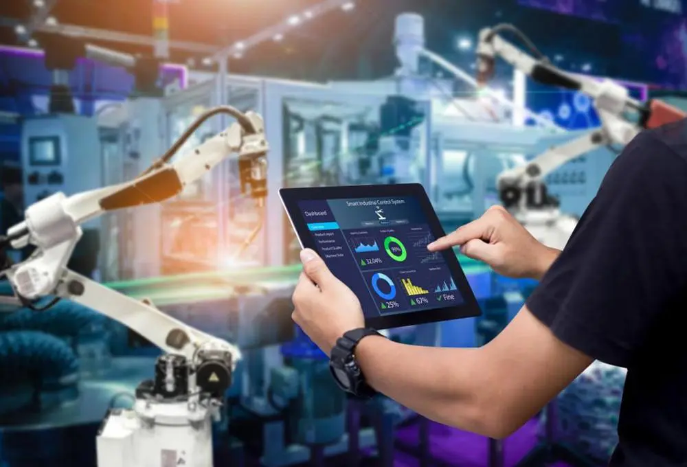
Ultra-Loss High-Frequency PCB for RF & Microwave Applications

In the rapidly evolving world of electronics, the demand for high-performance circuits operating at increasingly higher frequencies continues to grow. This trend has led to the development and widespread use of High Frequency (HF) Printed Circuit Boards (PCBs). These specialized PCBs play a crucial role in various applications, from telecommunications to aerospace technology. In this comprehensive guide, we’ll explore the intricacies of High Frequency PCBs, their properties, materials, design considerations, and applications.

What is High Frequency (HF) PCB?

High Frequency PCBs are specialized printed circuit boards designed to handle signals operating at frequencies typically ranging from 500 MHz to 2 GHz and beyond. These PCBs are engineered to maintain signal integrity and minimize losses at these high frequencies, making them essential for RF (Radio Frequency) and microwave applications.

Unlike standard PCBs, HF PCBs are built using specialized materials and design techniques to address the unique challenges posed by high-frequency signals, such as:

  • Signal loss
  • Electromagnetic interference (EMI)
  • Crosstalk
  • Impedance mismatches

High Frequency PCBs are critical components in various industries, including telecommunications, aerospace, defense, and medical equipment manufacturing.

๐Ÿ”ง High-Frequency PCB Engineering Tool
Professional Design Calculator & Reference Guide by RayPCB
Microstrip & Stripline Impedance Calculator
mm
mm
mm
GHz
Microstrip Impedance Formula (IPC-2141):
Zโ‚€ = (87 / โˆš(ฮตr + 1.41)) ร— ln(5.98H / (0.8W + T)) ฮฉ

Effective Dielectric Constant:
ฮตeff = (ฮตr + 1)/2 + (ฮตr – 1)/2 ร— (1 + 12H/W)^(-0.5)
High-Frequency PCB Material Database
Material Comparison Table
Material Dk @ 10GHz Df @ 10GHz Tg (ยฐC) CTE Z Freq Range Cost Index
Standard FR-4 4.2 – 4.5 0.020 – 0.025 130-140 50-70 ppm < 3 GHz
High-Tg FR-4 4.0 – 4.3 0.018 – 0.022 170-180 45-60 ppm < 5 GHz
Megtron 6 3.7 – 4.0 0.004 – 0.006 185 30-40 ppm 3-15 GHz
RO4003C 3.38 ยฑ0.05 0.0027 280+ 46 ppm 10-40 GHz
RO4350B 3.48 ยฑ0.05 0.0037 280+ 32 ppm 10-40 GHz
RO3003 3.00 ยฑ0.04 0.0013 N/A 24 ppm > 40 GHz
Taconic TLY 2.2 ยฑ0.02 0.0009 N/A 280 ppm > 77 GHz
Isola I-Tera MT40 3.45 0.0031 200 35 ppm 10-25 GHz
PCB Stackup Builder
Solder Mask Top – Green/Blue
L1 – Signal 1 oz Cu (35 ฮผm)
Prepreg 2116 (0.12mm)
L2 – Ground 1 oz Cu (35 ฮผm)
Core FR-4 (1.0mm)
L3 – Power 1 oz Cu (35 ฮผm)
Prepreg 2116 (0.12mm)
L4 – Signal 1 oz Cu (35 ฮผm)
Solder Mask Bottom
Stackup Summary
Total Thickness
1.57 mm
Signal Layers
2
High-Frequency Stackup Best Practice
For optimal high-frequency performance, place signal layers adjacent to ground planes. Maintain symmetrical stackup construction to prevent warpage. Use consistent dielectric materials throughout to minimize Dk variation.
Signal Loss & Attenuation Calculator
GHz
mm
mm
โš ๏ธ Loss Reduction Strategies
To minimize losses: Use low-Df materials (Df < 0.005), specify VLP or HVLP copper foil, increase trace width where possible, minimize via transitions, and consider embedded microstrip for better loss performance.
High-Frequency Via Design Calculator
mm
mm
mm
mm
Antipad Drill Pad

Cross-Section View

Via Electrical Parameters
Via Inductance
0.85 nH
Via Capacitance
0.35 pF
Resonant Frequency
9.2 GHz
Aspect Ratio
5.3:1
โœ… Via Design Guidelines for HF
Best practices: Keep aspect ratio below 10:1 for reliable plating. Use back-drilled vias to reduce stub resonance above 10 GHz. Place ground vias close to signal vias (within 0.5mm) for return current path. Consider via fencing for isolation in multi-channel designs.
HF PCB Cost Estimator
mm
mm
๐Ÿ’ก Cost Optimization Tips
Reduce costs by: Using hybrid stackups (Rogers for HF layers, FR-4 for others), optimizing panel utilization, reducing layer count where possible, and considering standard lead times. RayPCB offers competitive pricing for high-frequency materials.
High-Frequency PCB Design Guidelines
๐Ÿ“ก Transmission Line Design โ–ผ
Key Rules:
โ€ข Maintain consistent trace impedance (typically 50ฮฉ single-ended, 100ฮฉ differential)
โ€ข Keep trace width constant throughout signal path
โ€ข Avoid 90ยฐ corners – use 45ยฐ miters or curved traces
โ€ข Use ground coplanar waveguide (GCPW) for better isolation above 20 GHz
โ€ข Route critical RF traces on outer layers when possible
๐Ÿ”Œ Via Transition Optimization โ–ผ
Via Best Practices:
โ€ข Use back-drilling to eliminate via stubs above 10 GHz
โ€ข Place ground vias within 0.5mm of signal vias
โ€ข Minimize via inductance with larger pad sizes
โ€ข Use blind/buried vias to reduce stub length
โ€ข Consider via-in-pad for BGA breakout (filled and capped)
โšก Power Integrity for RF โ–ผ
Power Distribution Guidelines:
โ€ข Use solid ground planes – avoid splitting under RF traces
โ€ข Place decoupling capacitors close to IC power pins
โ€ข Use multi-value capacitor networks for broadband decoupling
โ€ข Keep power plane cutouts away from RF signal paths
โ€ข Consider stitching capacitors for ground plane connections
๐Ÿ›ก๏ธ EMI/EMC Considerations โ–ผ
Shielding & Isolation:
โ€ข Use via fencing around sensitive RF traces
โ€ข Implement guard traces for high-isolation requirements
โ€ข Maintain minimum 3ร— trace width spacing between signals
โ€ข Consider embedded shielding for critical circuits
โ€ข Use edge-plated shielding for maximum isolation
๐Ÿ“ Component Placement โ–ผ
Layout Strategies:
โ€ข Minimize trace length between RF components
โ€ข Group RF circuits by function (LNA, mixer, filter)
โ€ข Separate analog, digital, and RF sections
โ€ข Orient components to minimize trace bends
โ€ข Consider thermal management for power amplifiers
๐Ÿญ Manufacturing Considerations โ–ผ
DFM for High-Frequency:
โ€ข Specify tight Dk tolerance (ยฑ2% for RF layers)
โ€ข Request impedance testing with TDR
โ€ข Define copper roughness requirements (VLP/HVLP)
โ€ข Use symmetrical stackup to prevent warpage
โ€ข Consider material availability for production volumes
Frequency Band Quick Reference
Band Frequency Range Typical Applications Recommended Materials Max Df
L-Band 1-2 GHz GPS, Cellular High-Tg FR-4, Megtron 0.015
S-Band 2-4 GHz WiFi, Radar Megtron 6, I-Tera 0.008
C-Band 4-8 GHz 5G Sub-6, Satellite RO4350B, Megtron 7 0.005
X-Band 8-12 GHz Radar, Point-to-Point RO4003C, RO4835 0.004
Ku-Band 12-18 GHz Satellite Comm RO3003, RT/duroid 0.003
K/Ka-Band 18-40 GHz 5G mmWave, Radar RO3003, Taconic TLY 0.002
V-Band 40-75 GHz 60 GHz WiGig LCP, PTFE 0.0015
W-Band 75-110 GHz Automotive Radar LCP, Pure PTFE 0.001
HF PCB Design Review Checklist
Use this interactive checklist to ensure your high-frequency PCB design meets all critical requirements before sending to manufacturing. Click items to mark them complete.
๐Ÿ“‹ Material Selection (6 items) โ–ผ
Dk tolerance specified – Material Dk within ยฑ2% for impedance control
Loss tangent verified – Df appropriate for operating frequency
Thermal properties checked – Tg and CTE suitable for assembly process
Copper foil specified – Surface roughness (VLP/RTF) defined
Material availability confirmed – Lead time acceptable for schedule
Hybrid compatibility verified – If mixing materials, bonding verified
๐Ÿ“‹ Stackup & Impedance (5 items) โ–ผ
Impedance targets defined – 50ฮฉ single-ended, 100ฮฉ differential specified
Stackup symmetry verified – Symmetrical construction to prevent warpage
Reference planes identified – Signal layers have adjacent ground reference
Trace width calculated – Width verified with 2D field solver
Tolerance specified – ยฑ5% or ยฑ10% impedance tolerance defined
๐Ÿ“‹ Routing & Layout (7 items) โ–ผ
No 90ยฐ corners – All RF traces use 45ยฐ miters or arcs
Trace spacing adequate – Minimum 3ร— width between RF signals
Length matching verified – Differential pairs matched within spec
Reference plane continuous – No splits under RF traces
Via transitions minimized – Layer changes only where necessary
Ground vias placed – Return path vias within 0.5mm of signal vias
Via stubs addressed – Back-drilling specified where needed
๐Ÿ“‹ Manufacturing Notes (5 items) โ–ผ
Fabrication notes complete – All special requirements documented
Impedance coupon specified – Test coupon in panel for verification
Surface finish specified – ENIG/Immersion Silver/etc. defined
Solder mask clearance – RF areas with solder mask defined
IPC class specified – Class 2 or Class 3 requirements noted

Learn more about:

Properties of High Frequency PCBs

The performance of High Frequency PCBs is largely determined by their material properties. Let’s explore the key characteristics that make these PCBs suitable for high-frequency applications:

1. Low Dielectric Constant (Dk)

The dielectric constant, also known as relative permittivity, is a measure of a material’s ability to store electrical energy in an electric field. For HF PCBs, a low Dk is desirable because it:

  • Reduces signal propagation delay
  • Minimizes crosstalk between adjacent traces
  • Improves overall signal integrity

Typical Dk values for HF PCB materials range from 2.2 to 3.5, compared to 4.0-4.5 for standard FR-4 materials.

2. Low Dissipation Factor (Df)

The dissipation factor, also called loss tangent, represents the amount of energy lost as signals propagate through the material. A low Df is crucial for HF PCBs because it:

  • Reduces signal attenuation
  • Minimizes power loss
  • Improves the overall efficiency of the circuit

HF PCB materials typically have Df values in the range of 0.001 to 0.003, significantly lower than the 0.02 typical of FR-4 materials.

3. Low Dimensional Stability

Dimensional stability refers to a material’s ability to maintain its physical dimensions under varying environmental conditions. HF PCBs require excellent dimensional stability to:

  • Ensure consistent electrical performance across temperature ranges
  • Maintain precise impedance control
  • Prevent warpage and delamination

Materials used in HF PCBs often have a coefficient of thermal expansion (CTE) closely matched to that of copper, minimizing stress on the board during temperature fluctuations.

4. Low Moisture Absorption

Moisture absorption can significantly affect the electrical properties of PCB materials. HF PCBs use materials with low moisture absorption rates to:

  • Maintain stable dielectric properties
  • Prevent changes in impedance due to moisture uptake
  • Enhance long-term reliability, especially in humid environments

5. Chemical Resistance

HF PCBs often operate in challenging environments, necessitating good chemical resistance. This property ensures:

  • Durability during manufacturing processes
  • Resistance to degradation from environmental factors
  • Long-term reliability in various operating conditions

Materials Used for High Frequency PCB

The choice of material is critical in HF PCB design. Here are some of the most commonly used materials for High Frequency PCBs:

1. Rogers 4350B

  • Dk: 3.48 ยฑ 0.05 (10 GHz)
  • Df: 0.0037 (10 GHz)
  • Applications: Cellular base station antennas, power amplifiers

2. Rogers 4003C

  • Dk: 3.38 ยฑ 0.05 (10 GHz)
  • Df: 0.0027 (10 GHz)
  • Applications: Satellite communications, phased array antennas

3. Panasonic Megtron6

  • Dk: 3.4 (1 GHz)
  • Df: 0.002 (1 GHz)
  • Applications: High-speed digital, RF, and microwave applications

4. Rogers RO3003

  • Dk: 3.00 ยฑ 0.04 (10 GHz)
  • Df: 0.0010 (10 GHz)
  • Applications: Millimeter-wave circuits, automotive radar

5. Rogers RO3006

  • Dk: 6.15 ยฑ 0.15 (10 GHz)
  • Df: 0.0025 (10 GHz)
  • Applications: GPS patch antennas, satellite communications

6. Rogers RO3010

  • Dk: 10.2 ยฑ 0.30 (10 GHz)
  • Df: 0.0022 (10 GHz)
  • Applications: Patch antennas, RF/microwave circuits requiring high Dk

7. Taconic RF-35

  • Dk: 3.50 ยฑ 0.05 (10 GHz)
  • Df: 0.0018 (10 GHz)
  • Applications: Power amplifiers, LNAs, filters

8. Taconic TLX

  • Dk: 2.55 ยฑ 0.04 (10 GHz)
  • Df: 0.0019 (10 GHz)
  • Applications: Low-loss microstrip and stripline circuits

9. Rogers 5880

  • Dk: 2.20 ยฑ 0.02 (10 GHz)
  • Df: 0.0009 (10 GHz)
  • Applications: Aerospace and defense, millimeter-wave applications

10. Taconic TLC

  • Dk: 3.00 ยฑ 0.03 (10 GHz)
  • Df: 0.0030 (10 GHz)
  • Applications: Cost-effective alternative for less demanding RF applications

Design Tips of High-Frequency PCB

Designing High Frequency PCBs requires careful consideration of various factors to ensure optimal performance. Here are some essential design tips:

1. Routing Method

  • Use smooth curves instead of sharp 90-degree turns to minimize reflections
  • Implement differential pair routing for high-speed signals
  • Maintain consistent trace widths to control impedance

2. Routing Length

  • Keep high-frequency signal traces as short as possible
  • Match trace lengths for differential pairs and clock signals
  • Use serpentine routing for length matching when necessary

3. Use Less Number of Vias

  • Minimize the use of vias in high-frequency signal paths
  • When vias are necessary, use back-drilling to reduce stub length
  • Consider using buried or blind vias for critical high-frequency connections

4. Avoiding Crosstalk

  • Maintain adequate spacing between high-frequency traces
  • Use ground planes and guard traces to isolate sensitive signals
  • Avoid parallel routing of high-frequency signals over long distances

5. Implement Shorter Leads Between the Pins in a High-Frequency Circuit

  • Minimize lead lengths to reduce parasitic inductance and capacitance
  • Use surface mount components whenever possible
  • Consider using embedded components for critical high-frequency circuits

6. Add High-Frequency Decoupling Capacitors to the Power Supply Pins of IC Chips

  • Place decoupling capacitors as close as possible to IC power pins
  • Use a combination of capacitor values to cover a wide frequency range
  • Implement power plane sandwiches to reduce power distribution inductance

7. Isolate the Ground of High-Frequency Digital Signals and the Ground of Analog Signals

  • Use separate ground planes for digital and analog sections
  • Implement a single-point ground connection between digital and analog grounds
  • Consider using split planes for mixed-signal designs

8. Avoid the Formation of Loops Resulting from Routing

  • Minimize current loop areas in high-frequency circuits
  • Use solid ground planes to provide low-impedance return paths
  • Avoid creating slots or gaps in ground planes under high-frequency traces

9. Type of Transmission Line

  • Choose appropriate transmission line structures (microstrip, stripline, coplanar waveguide) based on the application
  • Maintain consistent impedance throughout the signal path
  • Use electromagnetic field solvers to optimize transmission line structures

10. Adopt Fly-by Topology/Daisy Chain Routing for DDR4

  • Implement fly-by topology for memory interfaces to reduce reflections
  • Use termination resistors at the end of each fly-by chain
  • Carefully match trace lengths within each byte lane

11. Adopt the 20H Rule to Minimize Plane Coupling

  • Maintain a minimum separation of 20 times the dielectric thickness between adjacent plane layers
  • Use cross-hatched planes to reduce plane resonances
  • Consider using multiple thin dielectric layers instead of a single thick layer

12. Ensure Proper Signal Impedance Matching

  • Calculate and maintain proper trace widths for desired impedance
  • Use impedance-controlled PCB fabrication processes
  • Implement proper termination techniques for high-frequency signals

HF PCB Design Considerations

Designing High Frequency PCBs involves addressing several critical factors to ensure optimal performance:

1. Select Low Profile Copper-Dielectric Interface

  • Use low-profile copper foils to minimize surface roughness
  • Consider reverse-treated foils for improved adhesion without sacrificing performance
  • Implement proper copper surface preparation techniques

2. Do Not Use FR4 for High-Frequency Applications

  • Choose specialized high-frequency laminate materials
  • Consider the trade-offs between performance and cost when selecting materials
  • Use hybrid stackups with high-frequency materials only where necessary

3. Radiation

  • Implement proper shielding techniques to minimize unwanted radiation
  • Use ground planes and vias to create effective RF enclosures
  • Consider the use of absorptive materials for critical applications

4. Absorption

  • Select materials with low loss tangent to minimize signal absorption
  • Account for frequency-dependent material properties in your designs
  • Use thicker dielectric layers for reduced absorption in critical signal paths

5. Signal Degradation

  • Minimize discontinuities in signal paths to reduce degradation
  • Use proper via design and placement to maintain signal integrity
  • Implement pre-emphasis and equalization techniques for long signal paths

6. Reflections

  • Match impedances throughout the signal path to minimize reflections
  • Use proper termination techniques for high-frequency transmission lines
  • Avoid abrupt changes in trace width or layer transitions

7. Coupling

  • Maintain proper spacing between high-frequency traces to minimize coupling
  • Use guard traces and ground planes to isolate sensitive signals
  • Implement differential signaling for improved noise immunity

8. EMI/EMC Compliance

  • Design with EMI/EMC compliance in mind from the start
  • Use proper shielding and grounding techniques
  • Consider the use of spread spectrum clocking to reduce EMI

9. Parasitic Capacitance

  • Minimize pad sizes and use tear-dropping to reduce parasitic capacitance
  • Carefully consider component placement to minimize unwanted coupling
  • Use 3D electromagnetic simulation tools to analyze and optimize designs

10. Harmonic Distortion

  • Use linear components in analog sections to minimize harmonic distortion
  • Implement proper filtering techniques for power supplies
  • Consider the use of balanced circuit topologies to cancel even-order harmonics

11. Common Mode Noise

  • Use differential signaling to minimize common mode noise
  • Implement common mode chokes for critical interfaces
  • Maintain symmetry in differential pair routing

12. Surface Tracking

  • Use conformal coatings to prevent surface tracking in high-voltage areas
  • Implement proper creepage and clearance distances
  • Consider the use of slot-patterning techniques for high-voltage isolation

High Frequency PCBs vs. High Speed PCBs

While often used interchangeably, High Frequency PCBs and High Speed PCBs have some distinct characteristics:

AspectHigh Frequency PCBsHigh Speed PCBs
Frequency RangeTypically 500 MHz to 2 GHz and beyondUsually up to 500 MHz
Signal TypeOften analog or RFTypically digital
Key ConcernsSignal loss, impedance controlSignal integrity, timing
MaterialsSpecialized low-loss materialsOften FR-4 or enhanced FR-4
Design FocusMinimize loss, control impedanceManage rise times, control reflections

Both types of PCBs require careful design considerations, but High Frequency PCBs often demand more specialized materials and manufacturing processes.

The Advantages of High Frequency PCBs

High Frequency PCBs offer several advantages for RF and microwave applications:

  1. Improved Signal Integrity: Low-loss materials and proper design techniques maintain signal quality at high frequencies.
  2. Higher Bandwidth: HF PCBs enable the transmission of more data in less time.
  3. Reduced Electromagnetic Interference: Proper design and materials help minimize EMI issues.
  4. Smaller Form Factors: HF PCBs often allow for more compact designs due to shorter wavelengths.
  5. Better Power Handling: Specialized materials can offer improved thermal management for high-power RF applications.
  6. Precision: HF PCBs provide the necessary precision for sensitive RF and microwave circuits.
  7. Flexibility: Various material options allow designers to optimize performance for specific applications.

The Applications of High Frequency PCBs

High Frequency PCBs find use in a wide range of applications across multiple industries:

  1. Telecommunications
    • 5G infrastructure
    • Satellite communications
    • Base station equipment
  2. Aerospace and Defense
    • Radar systems
    • Electronic warfare equipment
    • Satellite navigation systems
  3. Medical Devices
    • MRI machines
    • Ultrasound equipment
    • Surgical robots
  4. Automotive
    • Advanced driver assistance systems (ADAS)
    • Automotive radar
    • Vehicle-to-vehicle communication systems
  5. Test and Measurement
    • Network analyzers
    • Spectrum analyzers
    • High-frequency oscilloscopes
  6. Industrial
    • Industrial IoT devices
    • Wireless sensor networks
    • High-frequency power supplies
  7. Consumer Electronics
    • Smartphones
    • Wi-Fi routers
    • Bluetooth devices

As technology continues to advance, the importance of High Frequency PCBs in enabling high-performance electronic systems will only grow. By understanding the unique properties, design considerations, and applications of these specialized PCBs, engineers and designers can create innovative solutions to meet the challenges of our increasingly connected world.

Need a TG180 PCB- RayMing Has Got You

tg180 pcb

Size has always proved an important aspect of a printed circuit board across the globe. However, when I mention size, what comes to mind entails the need to have more components on less panel space, which, while true, fails to recognize the significance of size in terms of board thickness. In the present day and time, circuit board thickness has become a fundamental feature of PCB. No wonder you find circuit boards christened tg130, tg150, tg180, tg170, and tg260, among other customized board sizes.  

The article will focus on the high TG printed circuit boards and primarily on tg180 PCB.  Therefore, fasten your belts as we undertake this crucial PCB journey.

The TG180 Printed Circuit Board

As you might have encountered from time to time canvassing circuit board subjects, the word TG implies to the glass transition temperature, a key value in determining the point a material changes form from its glassy and rigid state into a rubbery and formless state, especially in the world of circuit boards.

Different glass transition temperature values exist for diverse PCB types, which play an instrumental role in coining their respective names. For instance, three wide categories of the TG range exist, consisting of standard or low TG, mid-TG, and high TG. A low and standard TG often encompass TG value below 130 degree Celsius. Middle or mid-TG values fall within the range of 130 degrees Celcius to below 170 degrees Celcius. Moreover, the high TG values entail any value equivalent to or above 170 degrees Celcius.

It, therefore, implies that the tg180 PCB falls under the high-TG category. So what makes up a tg180 printed circuit board?

The tg180 PCB, alternatively referred to as the fr4 tg180 printed circuit board, primarily consists of an fr4 board, layers of copper traces, and vias, among other crucial circuit board components. Suppose you want to understand the importance of the tg180 board among other high-TG boards. In that case, it becomes vital to know the influence of temperature on the board integrity both during the manufacturing process and when getting used to a particular function.

The temperature always plays a key role in the lamination process of PCBs, especially during the reflow process. It not only ensures a successful copper plating or trace embedding process but ensures that every circuit board maintains its integrity and performs as required upon completion of the assembly process. for instance, if you have designed your PCB with a TG material value of say 130 degrees Celsius then use more than 130 degree Celsius temperature while passing it through the reflow oven, then you will end up damaging the glass-epoxy resin of the board, which will damage everything else.  

Conversely, subjecting the PCB to inadequate temperatures during the manufacturing or assembly process will also interfere with the quality of the entire PCB, as it will not pass through quality assurance. Therefore, it implies subjecting the correct temperature through the manufacturing and assembly process to ensure a quality and efficient printed circuit board.

Another crucial area in that temperature plays a significant role entails the operating environment of the PCB. Circuit boards transmit electric, data, and other allied signals. Therefore when deployed where it transmits high current flows for extended periods besides sitting in high-temperature settings, the board can deform, subsequently leading to short-circuiting or interference with signal transmission. All these will render the PCB inefficient, thus making it useless. It all arises because an increase in temperature forces the circuit board materials to expand. Beyond their TG point, the material transitions into a rubbery and amorphous that can block through-holes or interfere with copper traces, thus impeding the operation of the circuit.

Specific Effects of Temperature on TG180 Board

shengyi-s1000h-material-pcb

As already established, the rf4 substrate provides the structural platform upon which the circuit traces get built in a printed circuit board. Rf4s have different grades depending on the temperature ranges they can handle. Whenever you subject an rf4 substrate to more temperatures than it can handle, then you will set yourself for failure. Below, a detailed explanation of how temperature impacts the rf4 material of the PCB.

  •  Crosslinking. It proves an instrumental fr4 material aspect, though it can always get affected when subjected to higher than designed temperatures. Temperatures beyond the TG point of the specific rf4 material diminish the crosslink density. Consequently, it influences segmental mobility material elements, thereby making it simpler for the solid glassy state to the amorphous and rubbery state.
  • Molecular weight. The molecular weight has a close association with the crosslink density. Whenever you surpass the fr4 TG value, the crosslink density diminishes. Consequently, it will reduce the molecular weight, which ultimately leads to a change in the material state.
  • Polymer flexibility. While the fr4 material has an allowance of always expanding and contracting based on temperature fluctuations, a temperature range beyond the TG value will become irreversible. It will impact the crosslinking density besides the molecular weight. Consequently, the polymer flexibility will drastically reduce, thereby compromising its capacity to operate seamlessly. For example, the size of the hole might enlarge or diminish, which can have adverse effects on the mechanical and electrical attributes of the printed circuit board design.

Therefore, it becomes crucial to function with an fr4 tg180, principally when the temperatures prove below 180 degrees Celsius. Additionally, it becomes ideal to remember the TB recommendations to stick with the materialโ€™s TB ratings that fall at least 20 to 25 degrees Celsius short of the projected TB value. If you adhere to this regulation, then you will achieve better-printed circuit board stability besides a seamless PCB operation when deployed.

Benefits and the Application of the TG180 PCB

As a high glass transition temperature PCB, the tg180 has obvious benefits and application areas. But what advantages does it present to you as a PCB option, and where can you use this type of printed circuit board? If you have a nice PCB budget, it will become wise to invest in a tg180 PCB. You do not need to feel silly and lose money on a TG material that cannot suit your printed circuit board needs besides the manufacturing conditions. Such a scenario will also set you back on time besides inconveniencing you.   

Attributes of a TG180 Printed Circuit Board

Temperature is instrumental in ensuring the stability of PCBs as any fluctuations of ensuring stability when trying to work with printed circuit boards. For illustration, an upsurge in temperature results in the material expansion of the rf4, thereby leading to a transformation in its properties. Therefore, at RayMing PCB and Assembly Company, we strongly endorse the utilization of tg180 printed circuit boards, primarily for systems that emit and operate within 150 and 180 degrees Celsius.

The company answers all your PCB inquiries regarding manufacturing, assembly, and fabrication services besides essential PCB products such as connectors, etc. You will get quality printed circuit board services and products. Additionally, the company has an established history of dealing in PCB products and services.

TG180 Material Attributes

A tg180 circuit board rf4 has several attributes, which makes it a viable component for PCBs. Some of the main attributes entail the following.

  • Diminished thermal expansion
  • The tg180 PCB undergoes very little dimension changes when it gets subjected to elevated temperatures. Therefore, it means that the materialโ€™s chances of breaking substantially diminish if the temperatures drop.
  • Enhanced resistance to moisture and heat
  • The tg180 material provides superior resistance to chemicals and mechanical elements, implying that your printed circuit board will have better stability than low and mid-level fr4 boards.

With all the information gathered, do you feel ideas on potential utilization of an fr4 tg180 PCB? High-temperature operations imply a need for a PCB that will not only handle the temperatures but work efficiently and seamlessly.

Applications of TG180 PCB

FULL PCB MANUFACTURING Quote

In this section, I have detailed the potential application areas for a tg180 printed circuit board.

  • Metal industries. Regardless of the element in question, metal proves vital in sustaining and easing our way of life. It can include steel, lead, titanium, aluminum, etc., in easing movement, health, housing, and other vital life aspects. But to mine and refine these metals into the ideal shapes, the industry has to cut, weld, grind and melt them. Such a process relies on machines that, in turn, rely on printed circuit boards. While temperatures in this industry process can vary, they usually prove high, and thus the need for a tg180 PCB. The high-Tg PCB will ensure a seamless operation of the machineโ€™s micro-controller.
  • Engine controllers. A tg180 PCB proves incredibly useful in the aerospace and vehicle industries, as they always need dependable controllers to improve engine efficiency. Its usefulness comes about because of the featured high RPM (rotations per minute) and prolonged running hours. Such as scenario increases the machineโ€™s unitโ€™s temperatures which can destroy the PCB, if not of an approved TG grade.

Advantages of Using a Tg180 PCB

  • Higher stability. You can bank on the better heat, moisture, and chemical resistance that tg180 printed circuit boards provide. Therefore, they also become more stable and with an increased boardโ€™s shelf-life.
  • Ultimate alternative for multi-layer PCBs. A printed circuit board possessing several layers proves dense and intricate. Such intricacy and density result in more heat generation that can effectively get handled by a tg180 printed circuit board.

Conclusion

If you want a PCB for intense and high-temperature generation operations, picking the tg180 printed circuit board can inspire an inspired decision. You can always get it in multiple layers from us. You only need to contact us.

The TG260 PCB – A Classical High Glass Transition Temperature PCB

TG260 PCB

The tg260 printed circuit board represents a high TG board, an important classification attribute of the base material in modern circuit boards. Besides the TG value, other crucial attributes such as dimensional stability and dielectric constant also play a significant role. As a printed circuit board designer, it becomes essential to understand the layout and design procedures and comprehend these crucial factors when designing your PCB.

The TG260

TG often implies the glass transition temperature, a crucial aspect of the board for performance and efficiency. TG acts as the standard parameter of temperature in printed circuit boards and gets measured in degrees Celsius. The glass transition temperature not only acts as the core value regarding a board materialโ€™s mechanical stability but one that guarantees its solidity.

So how can you define TG? It implies the temperature range that a polymer substrate gets to change or transition from a glassy and rigid material to an amorphous and soft state. It becomes essential to understand that the material forming the circuit board (normally an fr4) cannot burn but becomes unstructured when exposed to more than the designed for and expected temperature range.

A TG260 represents a typical high-Tg printed circuit board because of its tolerance to high-temperature ranges. It can tolerate up to a temperature value not exceeding 260 degrees Celsius without losing its board material structure integrity and functionality. However, it becomes equally essential to note that the optimum range for a tg260 falls above the temperature range of 170 degrees Celsius and 240 degrees Celsius. Ideally, the working temperature needs to fall shy of the tipping point by about 20 degrees Celsius.

You might wonder by this point why temperature proves a crucial aspect concerning the Tg of printed circuit boards. The temperature often plays a key role during the manufacture and seamless operations of a PCB. For instance, during the manufacturing process, the layers of copper often get incorporated through a temperature-enforced process inferred as lamination. Lamination becomes essential in ensuring the circuits get incorporated into the fr4 non-conductive substrate. Additionally, temperatures emitted from the circuit board during operations must fall within the recommended range to avoid any functionality issues within the PCB.

For an fr5 tg260 printed circuit board, the temperature emitted during the typical operation of the circuit and its surrounding areas has to fall between above 180 degrees Celcius to about 240 degrees Celcius. Otherwise, any temperature range that falls outside these parameters can compromise your PCB’s optimal functionality. Like operating temperatures, the tg260 PCB material needs to withstand the reflow oven process temperatures to ensure a study and a properly constituted printed circuit board that will operate seamlessly and at the optimum.

Specifications of a TG260 and Other High-TG PCBs

Isola P95 P25 PCB

The Tg value often corresponds to the tipping temperature point upon which the printed circuit board material changes. For instance, when the operating temperature surpasses the Tg value, the printed circuit board material will change from the early sturdy and solid state to a liquid and amorphous state. Such a change will negatively impact the capability of the circuit board, thereby interfering with its performance.    

Plenty of standard PCBs getting designed world-over to possess a Tg value that does not exceed 140 degrees Celsius and thus can withstand operating temperatures that slightly exceed 110 degrees Celsius. But as much as such printed circuit boards might possess the benefits that accrue from standardization, they prove inadequate for PCB products in extreme operating temperatures such as the ones witnessed in automotive industries. Such instances require printed circuit boards developed with an fr5 material instead of the fr4 material.  

But what does an fr4 material means? It implies the grade designation material of the fiberglass strengthened with epoxy and one that proves flame-retardant. Printed circuit boards with an fr4 material possess greater strength but provide higher heat resistance than local or standard PCB material equivalents. The fr4 comes under three distinct classifications, with the distinction between classes arising from the copper layer traces of the corresponding PCB. It includes multi-layered, dual-layered, and single-layered printed circuit boards.

So do you want a tg260 printed circuit board and lack ideas on how to go about it? Here, the best and easy way of doing it. Contact us at RayMing PCB and Assembly Company through the stipulated channels on our website’s home page to have answers to all your inquiries, manufacturing, fabrication, and assembly needs.

Why RayMing PCB and Assembly?

At RayMing PCB and Assembly Company, you will not only get the tg260 printed circuit board but a range of high-temperature tolerant printed circuit board products besides the associated fr4 or higher quality material services. The company has the relevant equipment, experience spanning fifteen years, and the technical human resource to execute fabrication of PCBs with resistance to high temperatures for diverse industries like the high-temperature electronics and automotive industries.

Common Materials Instrumental in the Manufacture of a TG260 PCB

Printed circuit boards with a glass transitional temperature value of tg260 require specific materials during their manufacturing. It includes the following.

  • In most cases, the tg260 printed circuit board will require the Rogers 4350 material type, unlike other high-Tg PCBs like tg175 and tg180 that can function with an fr4 S1141 and S1000-2M materials, respectively.
  • The tg260 PCB material also requires a high td value, typically 390 degrees Celsius. The td value proves higher than other high-Tg value materials.
  • The tg260 also needs a material component with a CTE-z value of 50 degrees Celsius, though it has no requirements when it comes to Td260 and Td288

The material aspects highlighted above often work in complementarity with the Tg value and also play a significant role in the performance of a printed circuit board. Because of this, we will detail a little about the dielectric constant value (Dt) and the coefficient of thermal expansion (CTE) value.

  • Coefficient of thermal expansion (CTE)
  • The value often plays a significant role in high-Tg printed circuit boards. It implies the expansion impact of the laminate when subjected to temperature changes on the printed circuit board’s operations. For instance, the expansion on the x-y plane can have drastic effects on any expansion-sensitive component placed and soldered on the board. A case in point includes a component such as the LGBA, which can destroy the PCBโ€™s solder joints during rapid expansion. Such an expansion mismatch between the board and the LGBA results in micro-cracking after some cycles of thermal tests.    
  • Dielectric constant (DK). It comes as a crucial yet often overlooked aspect by most printed circuit designers. It measures the signal integrity in a printed circuit board as signal dispersion often happens in the PCB. Signal dispersion often leads to distorted digital signals in PCBs, primarily if the device switches at high speeds.

It, therefore, becomes essential for you as a printed circuit board designer to contemplate the trade-off between performance, costs, and other material properties (such as the soldermask, substrate, and the laminate) when opting for the tg260 printed circuit board.

Application of the TG260 and other High-Tg Printed Circuit Boards

FULL PCB MANUFACTURING Quote

It always becomes useful for you as the designer to determine the lasting operating temperature of the tg260 board when it comes to exposure to elevated thermal loads. Such a determination will inform your decision to stick by this PCB material or opt for another material type. A crucial aspect that can help you determine this involves the glass transition temperature values of the printed circuit board material.

The most typical application areas of the high-Tg PCBs, such as the tg260, include the following.

  • Multilayer boards. Printed circuit boards with multiple layers often require an extensive reflow process that most PCB material Tg-value cannot support. For instance, the PCB will undergo multiple reflow oven processes to ensure a proper embedment of copper layers (traces), which can take its toll on fr4 materials lower than 170 degrees Celsius. Such high-temperature requirements during manufacturing will not only become compromising to the board’s structural integrity but also compromise its electric properties, such as damaging the copper traces or the through-holes.
  • Industrial electronics. Most industrial electronics get exposed to higher temperatures during operations, and thus the PCB needs to withstand these temperatures. What better method to ensure this than through the high-Tg PCBs? For instance, electric transformers that, besides the high heat, have to carry high current loads.
  • Automobile electronics. Most, if not all, automobiles emit high levels of heat. The printed circuit board in such machines has to operate within high temperatures and to necessitate this. It becomes essential to deploy high-Tg PCBs such as the tg260. ย 
  • Fineline trace structures. Such structures require a high-Tg material for its PCB to ensure that the high current and energy transmissions within the fine traces do not lead to a compromised system due to damage to the substrate.
  • High-temperature electronics. High-Tg printed circuit boards become an essential part of electronics that emit high temperatures. An excellent example includes a home appliance electronic in the form of a fridge that emits plenty of heat.

Final Thoughts

The tg260 represents a high glass transition temperature PCB that proves ideal for high-power equipment and appliances at home and in the industries. You, therefore, have to understand everything about the high- tg260PCB material to help you design and have it manufactured by a reputable company like us. We will always ensure that you do not regret ever choosing us. So good luck!  

Is possible to fabricate 50 layer PCB?

50 layer pcb

A printed Circuit Board (PCB) is mechanically an assembly of various electronic components embedded in a circuit board to help pass the channel of electrical energy in the assembly. The components fastened in this circuit are separated by small sections of insulation; this will avoid the risk of excessive heating to the other components. PCBs are of different kinds varying in size and thickness. Among all these multi-layered PCBs the one with the maximum number of multi-layered copper blanks is 50 layers Printed Circuit Board.

50 layers PCB is a series of consecutive double-layered copper plates. This overlapping in 50 layers printed circuit board can make a complex structure of the electrical network that will consume a heavy potential of doing multiple tasks uninterruptedly. The more the layers of the printed circuit board the more simple the system may work. Now here you need to look for an authentic answer to the question that is it possible to fabricate a 50 layers PCB?

Background:

First, you need to know that, the fact that 50 layer PCB is a complex network of series of multiple thick layers of copper sheets. This complex structure needs a very careful observation of threads of additional steps to complete its fabrication. A 50 layer PCB is integrated with a conductive copper and insulating material. These two conductive and insulating materials are combined and located alternatively to each other.

Is it possible to fabricate 50 layers PCB?

Isola FR408 PCB

Letโ€™s answer this frequently asked question by pondering over some important points of 50 layers PCB. As discussed above, the Printed Circuit Board (PCB) is a rigid board that supports several electronic components electrically and mechanically. Before having fabricating your PCB 50 layers, you need to know about these components thoroughly.

The 50 layers Printed Circuit Board (PCB) is formed of copper sheets laminated into a non-conductive substrate. The working of this modern tech 50 layers PCB is facilitated by a few capacitors, resistors, and active devices that are embedded in that substrate.

Yes! It is even possible to fabricate 50 layers PCB like any single-layered or doubled-layered PCB. But before, jumping into the guideline you must have known that the data entry required for the material used in fabrication should be in appropriate quantity.

How to make data analysis of the PCB components? — Must-Follow Steps before Fabrication

STEP: 1 Data Entry by Computer-Aided Design (CAD System)

In this step, CAD will assist the PCB data to be transferred to the manufacturer. PCB has a layout on a computer-aided design. CAD uses its internal storage for data formatting. With the aid of CAD, PCB transfers its standard output format layout to the manufacturers.

STEP: 2 Extended Gerber Files

The extended Gerber files are also called RS274X. The file is responsible to maintain a track record of all electronic components; the solder masks notations and copper layers. After the data has been collected and verified the process of fabrication could go the way around.

A STEP BY STEP GUIDE TO THE 50 LAYERS PCB FABRICATION PROCESS:

The Printed Circuit Board (PCB) is the most complex shape of technology. The copper plates inserted between the PCB vary in range from 1, 2, 10, 40โ€ฆ. and goes up to 50 copper sheets. This forms a thick even complex network of electronic components mechanically supported in a Printed Circuit Board. You will get the basic idea of how is it possible to fabricate 50 layers PCB in the following step-by-step guide.

  1. Determining the Nature of PCB

In the first step, it is essential to have sufficient information about the specifications needed for 50 layers PCB. The detailed information about the material specification and layer build-up is the first requirement. Only after that, the data entry could be passed on to the CAD for fabrication.

  • CAD Software Tooling

Now, this is the crucial step. The data transferred to the computer-aided design is now manufactured in the eye of keen observation. This step is critical because it is to be ensured that the PCB is produced by using the premium CAD-CAM Software Tools following the 50 layers PCB design and specifications.

  • Drilling

The process of drilling in 50 layers Printed Circuit Board is unique from other circuit boards. Keeping in view, the design and thickness of this circuit board the drilling machine is loaded with several different types of drills to make the holes in the printed circuit board. The holes are made into the copper plates by an automated drill which works on the state of the art technology to adjoin the top and bottom parts of the circuit together.

  • 50 Layers Lamination Process

Once, the inner layers of 50 layers PCB are built. These layers are now bound together with the assistance of prepregs. The lamination of the inner layers is completed by heating the laminate to 185 degrees/2 hours.

pection-aoi/

  1. X-ray
  • Hole Drilling

This is an additional step for the verification of the accurate drilling at the target positions in the centerline of the inner layers.

  • Electrolytic Plating Process

During fabrication, the electrolytic plating is processed into the holes made in inner layers by adding copper to it. During the electrolysis of copper, it turns into a cathode which is filled in the holes to help pass the electricity from top to the bottom and in between the layers. This process is also called Blackhole Lining.

FULL PCB MANUFACTURING Quote
  • Laser Imaging

This part of the fabrication of 50 layers PCB is very interesting. In this step, a laser machine is used to scan the blank surface and forms an image of the 50 layers Printed Circuit Board efficiently on a photosensitive film.

  • Tin Plating Process:

After the blanks have been electroplated in copper for about an hour the next step is to carry out these blanks into a tin tank for having been tin plated for about 10 minutes. In this process, a reverse current flows from the blanks to throw the small copper pieces down the holes. 

This is the final stage in fabricating a 50 layers PCB. In this stage, the 50 layers Printed Circuit Board is analyzed to compare the final image of the circuit board with the data previously recorded. The 50 layers PCB is now scanned by a camera and cross-checked by an operator to examine whether if the specifications are accurate or if any errors found are significant or not. This will ensure the high quality of the printed circuit board.

What Type Of Solder Resist Is Inserted In A 50 Layer PCB?

The Printed Circuit Boards have a permanent resin coating on the copper blanks. This resin-based coating is called Solder Resist which is defined as a photo imageable ink used to coat both sides of the Printed Circuit Board. The solder resists applied in a 50 layers PCB is applied over the entire outward surface of the Printed Circuit Board. The solder resists in 50 layers PCB is green in color.

50 Layers Printed Circuit Board | PROS:


There any many pros of having a 50 layers PCB. Following are some ways in which you may get to know how 50 layers are the best circuit board for long term use than its alternatives:

  1. High In Assembly Density:

Single-layer PCBs have low density than a 50 layers multiple PCB. Due to the high assembly density of 50 layers, PCB can perform its functions with an effective increase in speed and capacity. Moreover, the area of 50 layers PCB is reduced.

  1. Smaller In Size:

One of the unique features of 50 layers PCB is that we can increase its surface area by adding more layers to it. Unlike, single layers PCB we can only increase its surface area by increasing its size. This eventually exhibits that 50 layers PCB is far more effective to use in even smaller electronic devices.

  1. Lighter In Weight:

If you are concerned with the overall weight of the 50 layers PCB then you should know that the number of connectors used in a 50 layers PCB is far more reduced than a single-layer PCB. This also eventually reduced the weight of the overall circuit board. Hence, 50 layers PCB are more empirical for smaller electronic devices.

  1. Functionality:

50 layers Printed Circuit Board is advanced in its functionality. In comparison with a single layer PCB, 50 layers PCB stackup have a high capability of functionality. Its ultra-modern design, high capacity, improved quality, and speedy functionality make it the best Printed Circuit Board of all time.


Final Thoughts:

We are now certain that you have had a complete guide on how is it possible to fabricate 50 layers PCB? Today, 50 layers PCB are the most reliable and advanced in their design and accuracy for all electronic devices. This miniature 50 layers Printed Circuit Board is the improved version of the complicated structures of circuit boards these days.

Canada’s Top PCB Manufacturers: Medical & IoT Industry Leaders (2025)

canada pcb manufacturers

In the rapidly evolving landscape of technology, printed circuit boards (PCBs) form the backbone of electronic devices across various industries. As we approach 2025, Canada has emerged as a hub for cutting-edge PCB manufacturing, particularly in the medical and Internet of Things (IoT) sectors. This article delves into the thriving ecosystem of PCB manufacturers in Canada, with a special focus on industry leaders like M.I.S. Electronics PCB and the bustling Toronto PCB assembly scene.

The Rise of PCB Manufacturing in Canada

A Brief History of Canadian PCB Industry

Canada’s journey in PCB manufacturing began in the mid-20th century, paralleling the global rise of electronics. Over the decades, the country has cultivated a robust ecosystem of manufacturers, suppliers, and innovators, positioning itself as a key player in the North American market.

Current Market Trends and Projections

As we look towards 2025, the Canadian PCB manufacturing industry is poised for significant growth. Factors driving this expansion include:

  1. Increased demand for medical devices
  2. The proliferation of IoT technologies
  3. Government initiatives supporting high-tech manufacturing
  4. A skilled workforce with expertise in advanced electronics

Industry analysts project a compound annual growth rate (CAGR) of 3.5% for the Canadian PCB market from 2021 to 2025, outpacing the global average.

Top PCB Manufacturers in Canada

M.I.S. Electronics PCB: A Leader in Innovation

M.I.S. Electronics PCB has established itself as a frontrunner in the Canadian PCB manufacturing landscape. With a history spanning over three decades, the company has consistently delivered high-quality, innovative PCB solutions across various industries.

Key Strengths of M.I.S. Electronics PCB:

  1. Cutting-edge manufacturing facilities
  2. Expertise in complex, multi-layer PCBs
  3. Strong focus on research and development
  4. Commitment to environmental sustainability

M.I.S. Electronics PCB’s dedication to quality and innovation has made it a preferred choice for both medical device manufacturers and IoT companies seeking reliable PCB solutions.

Toronto PCB Assembly: The Hub of Canadian Electronics

Toronto has emerged as the epicenter of PCB assembly in Canada, hosting a cluster of manufacturers and assembly houses that cater to diverse industry needs.

Why Toronto Leads in PCB Assembly:

  1. Proximity to major tech companies and startups
  2. Access to a highly skilled workforce
  3. Well-developed supply chain infrastructure
  4. Supportive local government policies

Notable players in the Toronto PCB assembly scene include:

  • CircuitMaster Technologies
  • Axis Electronics
  • Protocase Electronics

These companies offer a range of services from prototype development to high-volume production, making Toronto a one-stop destination for PCB needs.

Other Notable PCB Manufacturers Across Canada

While Toronto and M.I.S. Electronics PCB are at the forefront, several other manufacturers across Canada contribute significantly to the industry:

  1. WestPCB Solutions (Vancouver):ย Specializing in high-frequency PCBs for telecommunications
  2. Circuits Quebec (Montreal):ย Known for their expertise in flexible PCBs
  3. Prairie Circuit Boards (Winnipeg):ย A leader in quick-turn prototyping services

Read more about:

Medical PCB Manufacturing in Canada

The Growing Importance of Medical PCBs

As healthcare technology advances, the demand for sophisticated medical PCBs continues to rise. Canadian manufacturers have been quick to adapt, offering specialized solutions for the medical industry.

Key Applications of Medical PCBs:

  1. Diagnostic equipment
  2. Patient monitoring devices
  3. Implantable medical devices
  4. Surgical robots and tools

Challenges and Innovations in Medical PCB Manufacturing

Producing PCBs for medical applications comes with unique challenges:

  1. Stringent Regulatory Requirements:ย Compliance with standards like ISO 13485 and FDA regulations
  2. High Reliability Demands:ย Ensuring consistent performance in critical healthcare settings
  3. Miniaturization:ย Developing smaller PCBs for implantable and portable devices
  4. Biocompatibility:ย Using materials safe for human contact

Canadian manufacturers are addressing these challenges through innovations such as:

  • Advanced clean room facilities
  • Implementation of rigorous quality control measures
  • Investment in high-precision equipment
  • Development of new biocompatible materials

Spotlight on Medical PCB Canada

Medical PCB Canada, a division of a larger electronics manufacturer, has carved a niche in producing high-quality PCBs for medical devices. Their success stems from:

  1. Specialized knowledge of medical industry requirements
  2. Partnerships with leading medical device companies
  3. Continuous investment in cutting-edge manufacturing technologies
  4. A dedicated team of biomedical engineers and PCB design experts

IoT Circuit Board Suppliers in Canada

The IoT Revolution and its Impact on PCB Manufacturing

The Internet of Things has transformed the landscape of electronic devices, creating new demands for PCB manufacturers. Canadian suppliers have risen to the challenge, offering innovative solutions for IoT applications.

Key Requirements for IoT PCBs:

  1. Low power consumption
  2. Small form factors
  3. Integrated wireless capabilities
  4. Durability for various environmental conditions

Leading IoT Circuit Board Suppliers in Canada

Several Canadian manufacturers have positioned themselves as go-to suppliers for IoT circuit boards:

  1. SmartBoardTech (Ottawa):ย Specializing in energy-efficient PCBs for IoT devices
  2. ConnectCircuits (Calgary):ย Known for their expertise in PCBs with integrated antennas
  3. IoTronics Solutions (Toronto):ย Offering customized PCB solutions for industrial IoT applications

These suppliers are driving innovation in the IoT space, contributing to Canada’s growing reputation as a hub for advanced electronics manufacturing.

Innovations in IoT PCB Manufacturing

Canadian manufacturers are at the forefront of several innovations in IoT PCB production:

  1. Additive Manufacturing:ย Using 3D printing technologies for rapid prototyping of IoT PCBs
  2. Flexible and Stretchable PCBs:ย Developing boards that can conform to various shapes for wearable IoT devices
  3. Integrated Power Management:ย Creating PCBs with built-in power optimization features
  4. Enhanced Security Features:ย Implementing hardware-level security measures to protect IoT devices from cyber threats

The Future of PCB Manufacturing in Canada

Emerging Technologies Shaping the Industry

As we look towards 2025 and beyond, several technologies are set to revolutionize PCB manufacturing in Canada:

  1. Artificial Intelligence:ย Optimizing PCB design and manufacturing processes
  2. 5G Integration:ย Developing PCBs capable of supporting high-speed 5G communications
  3. Nanotechnology:ย Creating ultra-miniature PCBs for advanced applications
  4. Green Manufacturing:ย Implementing eco-friendly processes and materials

Predictions for the Canadian PCB Market in 2025

Industry experts forecast a bright future for PCB manufacturing in Canada:

  1. Market Growth:ย Expected to reach CAD 2.5 billion by 2025
  2. Specialization:ย Increased focus on niche markets like medical and IoT
  3. Export Expansion:ย Growing exports to the United States and European markets
  4. Talent Development:ย Increased collaboration between industry and academia to nurture skilled professionals

Choosing the Right PCB Manufacturer in Canada

Factors to Consider

When selecting a PCB manufacturer in Canada, consider the following factors:

  1. Expertise:ย Look for manufacturers with experience in your specific industry
  2. Certifications:ย Ensure they have relevant quality and industry certifications
  3. Capabilities:ย Assess their ability to handle your required volume and complexity
  4. Turnaround Time:ย Consider their production speed and ability to meet deadlines
  5. Support Services:ย Evaluate their design assistance and post-production support
  6. Cost:ย Compare pricing, but don’t compromise quality for cost savings

Questions to Ask Potential Manufacturers

  1. What is your experience with [specific industry] PCBs?
  2. Can you provide samples or case studies of similar projects?
  3. What quality control measures do you have in place?
  4. How do you handle design revisions and prototyping?
  5. What is your typical lead time for production?
  6. Do you offer any value-added services like component sourcing or assembly?

Conclusion

As we approach 2025, Canada’s PCB manufacturing industry stands at the cusp of a new era of growth and innovation. Led by companies like M.I.S. Electronics PCB and the vibrant Toronto PCB assembly scene, Canadian manufacturers are well-positioned to meet the evolving needs of the medical and IoT sectors.

The combination of cutting-edge technology, a skilled workforce, and a supportive business environment makes Canada an attractive destination for companies seeking high-quality PCB solutions. As the industry continues to evolve, we can expect Canadian PCB manufacturers to play an increasingly important role in shaping the future of electronics on a global scale.

Whether you’re a medical device manufacturer looking for reliable, compliant PCBs or an IoT startup in need of innovative circuit board solutions, Canada’s diverse ecosystem of PCB manufacturers offers the expertise, quality, and innovation to meet your needs. As we move towards an increasingly connected and technologically advanced future, the Canadian PCB industry is poised to lead the way, driving progress and setting new standards of excellence in electronic manufacturing.

What Are IOT Devices ? Definition,Types, Applications.

IoT Devices

Introduction

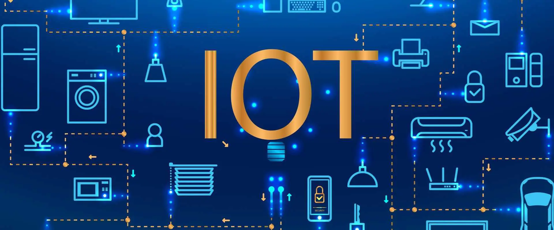
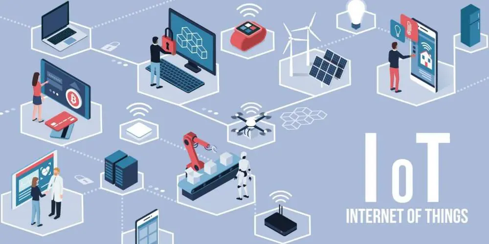
The Internet of Things, or IOT for short, refers to the billions of internet-connected devices and objects that collect, send and act on data. IOT devices are physical objects that are embedded with sensors, software and connectivity that allow them to connect, exchange data and be controlled remotely over the internet.

Some key things to know about IOT devices:

  • They have connectivity – they can connect to the internet directly or indirectly via a gateway. Common connectivity protocols include WiFi, Bluetooth, cellular and satellite.
  • They have sensors – temperature, motion, pressure, light etc. The sensors generate data that can be analyzed.
  • They have processing capabilities – to analyze data and execute commands. This may be a simple microcontroller or a powerful embedded computing system.
  • They generate and exchange data – with users, other devices, applications and services over the internet.
  • They can be controlled and accessed remotely – to change settings, give instructions, monitor status etc.

The number of connected IOT devices is growing exponentially. Estimates indicate there will be over 30 billion connected IOT devices by 2025. Let’s take a deeper look at what IOT devices are, the different types and their applications across industries.

What is an IOT Device?

IoT Device PCB BOARD

An IOT device is a computing device that connects wirelessly to a network and has the ability to transmit data. IOT devices have sensors that collect data, connectivity to transmit it, and sometimes the ability to receive and act on data.

More formally, an IOT device has three key capabilities:

  • Sensing – The device has sensors that detect events, changes and conditions in the physical environment like temperature, motion, pressure, location etc.
  • Connectivity – The device can connect to and exchange data over wired or wireless networks. This may be via WiFi, Bluetooth, cellular, satellite or other communication protocols.
  • Data exchange – The device can send sensor data over networks and in some cases also receive data and commands to actuators that can control mechanisms and systems.

The core components of an IOT device are:

  • Sensors and actuators – To detect events and conditions and enable responses. Sensors convert physical properties into electrical signals. Actuators convert electrical signals into physical actions.
  • Processors – To execute code that processes sensor data and controls actuators. Can range from basic microcontrollers to advanced microprocessors and systems-on-chip.
  • Communication hardware – To connect to wired and wireless networks. Can include chips, antennas, ports etc.
  • Software – Firmware and applications to manage device operation, data exchange protocols, process data and enable communication.
  • Operating system – Some devices have compact real-time operating systems suited for IOT devices.
  • Security features – Hardware and software to secure device communications and data transmissions.
  • Power supply – Battery, power harvesting or AC power connection.

IOT devices take input from the physical world through sensors, process it and transmit it over networks. The connectivity allows them to exchange data with applications, services, other devices and users to enable useful functions.

Types of IOT Devices

There is a vast variety of IOT devices for different applications across industries like home, transportation, healthcare, manufacturing, retail, energy and more. IOT devices can be classified into different types based on factors like mobility, size, communication protocols, power source and functionality. Here are the main categories of IOT devices:

Consumer IOT Devices

These are IOT devices intended for personal and home use such as:

  • Smart home devices – Smart speakers, smart displays, smart security cameras, video doorbells, smart thermostats, smart switches, smart locks, smart appliances etc. Most connect via WiFi and are controlled via smartphones and home assistants like Alexa.
  • Wearable devices – Fitness bands, smart watches, smart glasses and health monitoring devices that connect via Bluetooth to smartphones. Measure data like steps, heart rate, sleep etc.
  • Smartphones and tablets – Modern mobile phones and tablets with cellular, WiFi, Bluetooth and GPS are IOT devices with rich sensing capabilities.
  • Entertainment devices – Media streaming dongles, smart TVs, game consoles, and connected audio devices are IOT entertainment systems.

Industrial IOT Devices

These IOT devices are designed for industrial environments and applications:

  • Sensors – Temperature, pressure, gas, flow, level, proximity, motion sensors used for monitoring industrial equipment and infrastructure. Most connect through wired interfaces.
  • Actuators and controllers – Valves, motors, pumps, relays and industrial automation controllers that actuate based on sensor data.
  • Tracking devices – RFID readers, asset trackers, location beacons and video surveillance cameras for tracking assets, inventory and people.
  • Industrial mobile devices – Ruggedized tablets, handheld scanners, wearables designed for factory and field work. Connect via WiFi, cellular and Bluetooth.
  • Gateways and routers – Hardware devices that enable legacy industrial systems and equipment to connect to networks and the cloud.

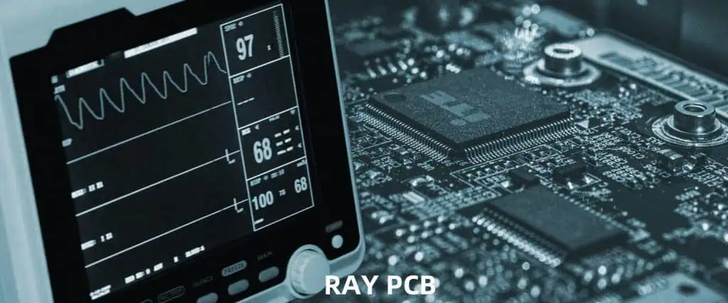
Medical and Healthcare IOT Devices

IOT is transforming healthcare with devices like:

  • Wearable devices – Activity trackers, smart watches, ECG and EKG monitors, glucose monitors etc. for health and fitness monitoring.
  • Implantable devices – Implantable sensors, pacemakers, insulin pumps etc. with connectivity for real-time diagnostics and delivery of therapies.
  • Telehealth equipment – Monitoring devices to track vital signs paired with communication devices for remote healthcare.
  • Wireless medical devices – Inhalers, pumps, monitors that connect to smartphones and healthcare systems for data tracking.
  • Smart medical equipment – Connected imaging machines, beds, ventilators and medication systems that integrate with healthcare IT systems.

Automotive and Transportation IOT Devices

Connected vehicles contain dozens of IOT devices and sensors:

  • Infotainment systems – Dashboard touchscreen displays, Bluetooth connectivity, WiFi hotspots and navigation systems.
  • Telematics devices – Black boxes and data loggers that record driving data and connect to backend systems via cellular.
  • ADAS sensors – Cameras, RADAR, LIDAR and ultrasonic sensors that enable advanced driver assistance systems and self-driving technology.
  • Diagnostic devices – OBD-II port connectors that plug into vehicles to monitor vehicle health and driving data.
  • Fleet management trackers – Hardwired asset trackers and GPS locators used to monitor commercial trucking fleets.
  • Electric vehicle systems – Charging stations, battery optimizers and range monitoring systems specific to connected electric vehicles.

Network-Connected Devices

These IOT devices connect end points to wired and wireless networks:

  • Connected sensors – Environmental sensors for air quality, noise, pollution levels that relay data via WiFi, LoRaWAN etc.
  • Smart meters – Energy meters, gas & water meters that connect to utility networks to transmit consumption data.
  • Smart grid devices – Distributed energy resource controllers, grid sensors and switches for power management.
  • ** routers** – Network routers, switches, gateways and modems that extend connectivity.
  • 5G Cells – Next generation 5G base stations and small cells that enable cellular IOT.
  • Satellite modems – Satellite transmitters and receivers that connect assets and infrastructure in rural areas.

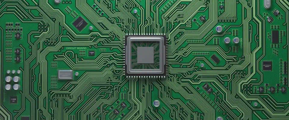
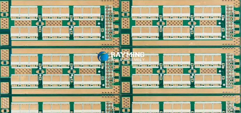
IOT Device Components

IOT devices contain a range of electronic components that enable sensing, connectivity, power and intelligence:

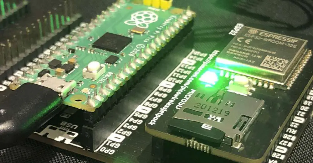
Microcontroller Units (MCUs) – Tiny low powered microcontrollers specially designed for IOT devices. Examples: ARM Cortex-M, Microchip AVR, NXP Kinetis.

Sensors – MEMS accelerometers, gyroscopes, compasses, microphones, environmental sensors, biosensors etc.

Wireless radios – WiFi, Bluetooth, ZigBee, LoRa, NB-IoT, LTE chipsets and antennas tailored for IOT.

Power supplies – Batteries, energy harvesting modules, charging circuitry optimized for long battery life.

Memory and storage – NOR and NAND flash memory chips to store firmware and data.

Real-time operating systems (RTOS) – Lightweight operating systems like FreeRTOS, ThreadX and RIOT OS designed to run on MCUs.

Security chips – Hardware chips that provide security functions like encryption, authentication and access control.

Interfaces – UART, SPI, I2C, USB interfaces to connect sensors, actuators and peripherals to MCUs.

IOT device hardware provides the core functionality while software and connectivity enables intelligence. The components come together on circuit boards like single board computers and system-on-modules tailored for IOT products.

IOT Software Platforms

embedded iot

In addition to hardware, IOT software platforms provide vital capabilities:

Device Management

To remotely configure, monitor, control and update connected device fleets. Leading platforms include AWS IoT Core, Microsoft Azure IoT Hub and Google Cloud IoT Core.

Connectivity Management

To connect and manage cellular, satellite or low power wide area networks like Lora and Sigfox. Platforms like EMnify, Soracom and Twilio provide global connectivity.

Data Management

IOT platforms to securely ingest, process and analyze huge volumes of IOT data in real time. Examples include AWS IoT Analytics, Google BigQuery and Azure Time Series Insights.

Application Enablement & Development

Tools to build, deploy and scale IOT applications without managing infrastructure. Platforms like AWS IoT Greengrass, Microsoft Azure IoT Central and Google Cloud IoT make IOT application development easier.

IOT platforms provide cloud-based tools and managed infrastructure tailored to IOT use cases. They help manage connections, data, analytics, visualization and workflows across millions of endpoints.

IOT Device Connectivity Protocols

There are a range of wireless technologies used to connect IOT devices depending on the use case, power needs and network requirements:

WiFi – Popular for consumer electronics and industrial devices. Provides high bandwidth with medium range. Supported by widespread infrastructure.

Bluetooth/BLE – Ubiquitous in wearables and peripherals. Very low power consumption for battery-operated devices. Short range up to 50m.

Cellular – Includes 2G/3G/4G/5G networks. Long range connectivity globally. High power consumption but enables mobility.

LoRa/Sigfox – Low power wide area networks for sensors and trackers. Run on unlicensed spectrum with km-range connectivity.

Zigbee – Mesh protocol for smart homes and buildings. Low power consumption with self-healing mesh reliability.

NB-IoT/LTE-M – Cellular LPWAN technologies optimized for IOT. Low power and extended coverage.

Satellite – Provides global connectivity in rural areas. Latency can be high but useful for assets in remote locations.

Ethernet – Widely used for fixed industrial assets and hardware connections. Provides reliable high bandwidth communication.

Choosing the right protocol depends on power needs, communication frequency, bandwidth needs, network coverage and cost. IOT devices may use multiple protocols to transmit telemetry data, receive notifications and enable over-the-air updates.

IOT Device Management

Managing hundreds or thousands of IOT devices in the field requires specialized device management capabilities:

  • Provisioning and Authentication – Securely configure and register device credentials on first boot.
  • Configuration Management – Remotely configure device settings like communication parameters, sampling frequency etc.
  • Monitoring and Diagnostics – Get real-time and historical insights into device health and activity.
  • Software and Firmware Updates – Securely update device software and firmware versions over the air.
  • Command and Control – Remotely send commands to devices like changing states, triggering actions etc.
  • Decommissioning – Retire and disconnect devices no longer in use while retaining data.

Leading IOT platforms provide these device management capabilities at scale across global networks. AWS IoT Core, Microsoft Azure IoT Hub, Google Cloud IoT Core are popular cloud-based IOT device management platforms.

On the hardware side, secure chips like hardware security modules, trusted platform modules and secure elements provide tamper-resistant secure storage for device credentials, encryption keys and access control.

IOT Device Security

ESP IoT Board
ESP IoT Board

Security is a major concern with IOT devices given the potential risks of hacking:

  • Device vulnerabilities – Weak default passwords, unpatched firmware, lack of encryption are common issues.
  • Data vulnerabilities – Unencrypted data transmission and storage can expose private data.
  • Identity spoofing – Faked device identities can infiltrate networks.
  • Denial of service – Devices with weak security can be compromised to execute DDoS attacks.
  • Takeover – Hacked devices could be used to pivot and access enterprise or home networks.

To secure IOT devices:

  • Use trusted hardware modules and secured operating environments.
  • Perform penetration testing to identify vulnerabilities.
  • Ensure secure boot, code signing and verified updates.
  • Encrypt data transmission and storage.
  • Use strong authentication, access control and certificates.
  • Monitor devices for suspicious activity and anomalies.
  • Isolate IOT networks and limit external access.
  • Maintain physical security of devices.

A defense-in-depth approach is required to secure the ecosystem of IOT device hardware, connectivity, platforms and data flows.

Applications of IOT Devices

Let’s look at some of the many applications of IOT devices across different industries:

Smart Homes

  • Smart speakers – Voice assistants like Alexa and Google Home for information, entertainment and appliance control.
  • Smart lighting – Connected LED bulbs with wireless control for automation and energy savings.
  • Smart switches and plugs – Remotely control appliances and enable scheduled on/off.
  • Smart security – Monitor home remotely via cameras. Control security systems.
  • Smart locks – Keyless entry. Access control via smartphones.
  • Smart thermostats – Adjust temperatures based on occupancy and preferences to conserve energy.
  • Smart sensors – Detectors for water leaks, open doors/windows, smoke, CO.
  • Smart appliances – Refrigerators, ovens, robots with connectivity for control, diagnostics.

Industrial IOT

  • Predictive maintenance – Vibration sensors on motors and pumps to monitor equipment health in real time.
  • Inventory management – RFID and barcode scanners to track items through facilities.
  • Quality assurance sensors – Test product quality on assembly lines with connected instruments.
  • Environmental monitoring – Sensors that track temperature, humidity throughout facilities.
  • Asset tracking – Real-time location of equipment and vehicles in yards and warehouses via tags.
  • Fleet management – GPS trackers and telematics for tracking vehicles, fuel usage, driver behavior.
  • Smart meters – Monitor utility usage on factory floors in real-time.
  • Process optimization – Sensors that improve throughput, material handling, supply chain logistics.

Smart Cities

  • Smart lighting – Intelligent street lights with adaptive brightness, tracking and fault detection.
  • Water management – Monitor pipe pressure, leaks, reservoir levels with IoT sensors.
  • Waste management – Connected trash bins optimize pick-up routes.
  • Environmental monitoring – City-wide air quality, noise monitoring informs public health initiatives.
  • Smart parking – Sensors on lots detect availability and direct drivers.
  • Traffic management – Adaptive signals, real-time congestion mapping, public transit tracking.
  • Public safety – Connected cameras, emergency response coordination.
  • Smart infrastructure – Monitor structural health of bridges, railways, airports.

Healthcare Systems

  • Remote patient monitoring – Wearable sensors allow patients to be monitored at home, improving outcomes.
  • Asset management – Real time location of medical equipment reduces losses.
  • Inventory management – RFID tracking for pharmaceuticals and supplies.
  • Environmental monitoring – Ensure stable temp, humidity for drugs, tissue samples.
  • Patient flow optimization – Tracking and visualization of patient journeys through hospital improves throughput.
  • Infection control – Hand hygiene compliance monitoring reduces hospital acquired infections.
  • Connected imaging – XRay and MRI systems integrated with healthcare IT systems.

Agriculture and Farming

  • Soil sensors – Measure moisture, nutrition levels to optimize watering and improve crop yield.
  • Livestock tracking – Monitor the health and location of cattle via wearable tech.
  • Smart greenhouse – Automated control over lighting, humidity, irrigation based on conditions.
  • Cold chain monitoring – Ensure optimal storage and transport temperatures for perishables.
  • Farm vehicle tracking – Self driving tractors. Fleet management for machinery.
  • Smart irrigation – Automated irrigation controlled via data from field sensors.

Retail and Logistics

  • Smart shelves – Digital shelving displays stock levels in real time. Detect low inventory.
  • Supply chain tracking – RFID and GPS to track location and condition of goods in transit.
  • Smart checkout – Frictionless retail where customers are automatically charged via app.
  • Inventory robotics – Robots equipped with sensors assist in warehouse inventory counting.
  • In-store analytics – Sensors track customer foot traffic patterns within store.
  • Food management – Monitor refrigerator and freezer temperature, humidity and air quality.

Energy Management

  • Smart grids – Sensors and automation across transmission and distribution for efficient delivery.
  • Smart meters – Meters enable consumers to track energy usage patterns in real-time.
  • Renewables monitoring – Assess output and performance of solar, wind installations via sensors.
  • Predictive maintenance – Monitor oil pipelines, wind turbines and power assets in real time.
  • Asset tracking – GPS tracking devices on high value equipment and vehicles.
  • EV charging networks – Software platforms to manage electric vehicle charging stations.

These are just some examples of the broad applications of IOT devices across industries. The use cases for IOT are constantly expanding as technology evolves.

The Future of IOT Devices

What does the future hold for IOT devices and applications? Some key trends:

  • 5G and new spectrum – Faster 5G networks and new spectrum like CBRS will enable next-gen IoT.
  • AI at the Edge – More analytics and

Top 10 IoT Devices in Electronic Application

Technology continues to change the work. The dawn of the year 2000 was the start of a new era, as far as the applications of the technology were concerned.

It started with the bubble of the dot.com phase that led to the evolution of the Internet. This is followed by the proliferation of social networks and multiple websites.

Now, we are talking about the application of advanced technology in the form of the Internet of Things (IoT). We are talking about a new system of connecting most of our devices to the Internet.

The Internet is smart. The Internet is reliable. The Internet is for everyone and everything!

In this article, you will find out more about the top 10 Internet of Things (IoT) devices that are not only becoming more popular in 2021 but are also making disruptions in important economies.

What is IoT?

FULL PCB MANUFACTURING Quote

So, what is this IoT that everyone in the tech world is talking about? Internet of Things or IoT for short refers to a system of interrelated computing devices that are physical.

IoT is also a network of objects, digital machines, people, or animals. Those are generally classified as and called Things.

This network of objects is embedded with sensors and Unique Identifiers (UIDs) that are connected to connect and exchange data from those Things.

The transmission of data is usually done from those devices or things to the network. Therefore, human intervention is not always needed.

What is IoT Devices?

Simply put, IoT Devices are the pieces of machines, hardware, gadgets, sensors, and appliances that are connected to the Internet. The connection is done in a way that the IoT Devices can transfer over the network/Internet without requiring additional programming.

The Top 10 IoT Devices to Watch Out for in 2021

Although there are several IoT Devices, not all of them function the same way. Likewise, some IoT devices have been able to gain more traction in recent months than the others have.

Thus, we present to you, the top 10 IoT Devices that will feature the most in the technological sector in 2021:

1. IoT Healthcare Devices

Picture a world where patients can now receive instant information on their health status, even if they are many miles away from the nearest hospital or clinic.

Is it possible? Yes, it is!

Wearable healthcare devices make it possible. The role played by the Internet of Things (IoT) in this regard cannot be underestimated.

Now, these IoT healthcare devices can collect data from the Internet where they are connected. This way, patients and those at the risk of certain health conditions will be able to have more control over their health.

Thus, IoT healthcare devices are one of the IoT devices to look out for in 2021. For emphasis, let us talk about a couple of these IoT healthcare devices and the inputs they are making to make the healthcare system better.

Monitoring Medical Adherence

Is it possible for a device to monitor whether a patient has taken his or her medication or not? Yes, it is because certain IoT devices have been developed to look into this.

You would agree that illnesses can be treated faster if the patients took their medications religiously. However, that is not always the case because some patients tend to either forget or decide not to take their medications.

However, some healthcare IoT devices have been manufactured to tackle this. These devices can go as high as determining whether the patient has taken the medication.

The determination is usually by monitoring the swallowing of the capsules or tablets, saliva swallows and even drinking water after swallowing the capsules.

The medical adherence IoT devices are designed in different ways with the most common being wearable smart necklaces.

IoT Healthcare Devices for Glucose Tracking

Blood sugar or glucose levels can now be tracked with ease with dedicated IoT devices used for tracking glucose.

These glucose tracking IoT devices are sometimes designed with automated insulin delivery systems and glucose monitoring systems that can be used to check the amount of glucose in the body.

Examples of these IoT glucose trackers are:

  • Eversense
  • Dexcom

2. Industrial IoT Devices

Industrial IoT Devices

There is no doubt that the industrial sector is one of the economic sectors that benefit the most from the application of the Internet of Things.

You must have heard about Industry 4.0. It simply refers to the next industrial revolution where Internet-enabled devices will be mostly used to automate tasks in our industries.

Of course, the manufacturing or production of most products is done in industries. So, you can imagine the innovations that would be in place as soon as more IoT devices are deployed for use in our industries.

Likewise, some industrial IoT devices are tipped to be used the most in 2021. These are some of them:

Kiva Technology

At the core of the Industrial Internet of Things (IIoT) is the innovations made by the tech giant and global e-commerce disruptor, Amazon.

Kiva Technology is one of the huge investments made by Amazon to aid warehouse reinvention.

Kiva Technology was acquired by the company (Amazon) in 2012 and it is used for locating the shelves of products.

The technology is manned by robots, which is the reason why Amazon was able to cut down on its operating costs by 20% as of 2014.

Self-Driving Tractors

The manufacturing sector may be receiving most of the attention, but it is not the only industry that is being disrupted by the Internet of Things (IoT).

The agricultural sector is also disrupted by IoT and John Deere is one of the companies that is leading the new era of agriculture.

The company had in 2015, rolled out self-driving tractors that now make it easier for farmers to go about their businesses.

That is not all. The company also deployed telematics technology, which can be used for discovering potential mechanical issues in the tractors. This way, the predictive feature of the technology can pick out the issues for immediate fixing.

Industrial Internet of Things (IIoT) can also be applied in the following areas of industrial production:

  • Monitoring of equipment damages
  • Automation of the inventory monitoring for the maintenance of efficient workflow.
  • Automated and remote equipment monitoring
  • Supply-chain optimization
  • Faster changes and improvements in the industrial business model
  • Predictive maintenance

3. AWS IoT Devices

Amazon is not only a company that deals in the online distribution of goods and services. The brand also focuses on the development of Internet of Things (IoT) devices via the dedicated Amazon Web Services (AWS).

AWS IoT refers to the provision of cloud services by Amazon. These cloud services are used to connect Internet of Things (IoT) devices to both Amazon Web Service (AWS) cloud services and other devices.

Besides, AWS brings together both Internet of Things (IoT) and Artificial Intelligence together so that the two can be combined to create scalable solutions to cloud computing and IoT offerings.

Now, several AWS IoT devices are delegated for use in different sectors. They include:

FreeRTOS

FreeRTOS is one of the IoT devices manufactured and deployed by Amazon Web Services (AWS).

FreeRTOS is an Operating System (OS) specifically designed for use in Microcontrollers (MCUs). The impact of this IoT is that it makes it simpler for low-power and small edge devices to be programmed, deployed, secured, and connected to cloud services. The FreeRTOS AWS IoT also makes it easier to manage the operations of the microcontrollers from the same interface.

AWS IoT Device Management

It is one thing to develop and deploy an Internet of Things (IoT) device. It is another thing to manage the device effectively so it continues to function optimally.

That is the concept behind AWS IoT Device Management. It is an IoT device that allows you to securely onboard, monitor, organize and remotely take control of the other IoT devices that are connected to it.

AWS Partner Device Catalog

Amazon Web Services IoTs do not work alone. There may be a need for the developers or users to connect to other IoT devices for maximum productivity.

This informs the reason behind the development of the AWS Partner Device Catalog. It is a dedicated IoT used for finding both hardware and devices that can work well with Amazon Web Service (AWS).

Once that is confirmed, developers will then be able to use the AWS Partner Device Catalog to explore and build the IoT devices of their choice.

AWS IoT Core

Internet of Things (IoT) devices need to connect easily on the Internet. That is what the AWS IoT Core does.

It is a managed cloud service that paves the way for connected/IoT devices to securely and easily interact with both IoT devices and cloud applications.

4. IoT Home Devices

iot home devices

Ever heard of Smart Homes? Have you wondered what it means for homes to be smart? It simply means that those homes are equipped with some of the best IoT devices that can be used to raise the IQ or functionality of the home.

Today, there are several IoT devices for our homes. These range from Wi-Fi locks to security cameras and down to smart lighting.

The idea is to make the home connected in a way that most of the devices or appliances in the home can work well with the use of the Internet.

You can now automate your house with some of the best smart home devices.

The examples below are some of the top IoT devices that would be used in most homes around the world in 2021:

Nest Protect

Nest Protect is a smart smoke detector that helps you to stay safe around your house. You may not always be lucky to be within reach when a fire breaks out in your home.

However, Nest Protect does a great job of detecting carbon monoxide and smoke. The device would then turn on the spoken alerts and the lights around that area

This way, you will be able to have a visual cue of the direction of the smoke/carbon monoxide so you can get out of the house on time.

Hamilton Beach Smart Coffee Maker

Home IoT devices are much more than just smart door locks and smart bulbs. Instead, smart coffee makers are also a part of the deal.

The Hamilton Beach Smart Coffee Maker is an example of how smart the home can be. This coffee maker can brew as much as 12 cups of coffee at once.

All you need is to issue a voice command and everything will be set!

5. Edge Devices IoT

Edge Devices are pieces of hardware or equipment that are used to transmit data from the local network to the cloud. This way, it will be easier to connect your Local Area Network (LAN) to a Wide Area Network (WAN) or an external network.

An edge device also serves the purpose of providing an entry point into a service provider or enterprise core networks.

Generally, Edge Devices serve as the intermediary or smart gateway for languages/protocols used by both local devices and cloud computation. That way, it will be easy for secure information transmission to be done for both.

On the one hand, local networks are NFC, Bluetooth, Zigbee, and Wi-Fi. On the other hand, cloud network uses specific protocols, such as HTTP, AMQP, CoAp, and MQTT.

From the above, it is clear that both the local and cloud networks have different protocols for data transmission. Therefore, there is a need for common ground or interface for the data from the local networks to be transmitted to the cloud networks. It is this interface that is called Edge Devices or gateways.

Some examples of Edge Devices are:

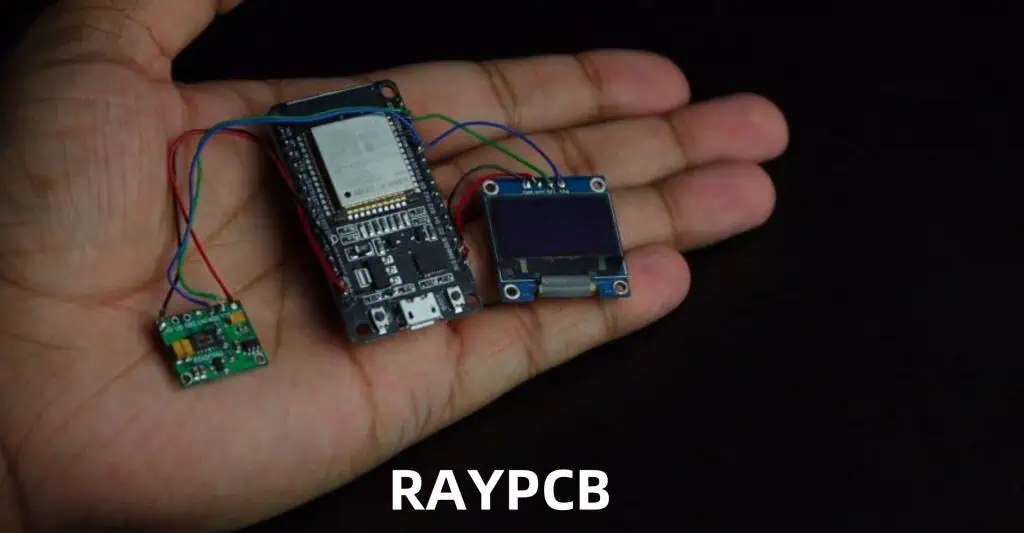
6. IoT Wearable Devices

Internet of Things (IoT) devices are not limited to just physical devices usable in industries and homes.

You can also wear IoT. This is because of the Wearable IoT Technology that makes it possible for people to wear electronic devices that function both as mere devices and trackers.

Wearable Technology refers to electronic devices that are developed with tracking and analytical features. This ensures that the IoT Wearable Devices analyze the wearers (individuals wearing) them, as well as transmit the information/data obtained from the individuals.

The relevance of Wearable Devices is that the devices can accurately track and relay relevant personal data, such as the exercise and medical data of the person(s) putting on the device.

This would, in turn, be used to help the individual to upgrade the lifestyle.

Here are some examples of Wearable (IoT) devices you can come across in 2021:

  • Gaming Wearable, such as Haptic vests, Virtual Reality (VR) Headsets
  • Smart clothing that monitors your temperature, movement, pulse, nutrition, respiration rate, sleep, and heart rate.
  • Fitness trackers are designed as wrist bands to track GPS, monitor your sleep level, step count, nutrition (including calorie intake), moving distance, and blood sugar.
  • Smart Shoes
  • NFC Smart Ring
  • Smart Nicotine Patch devised with Nicotine Replacement Therapy for delivering nicotine into the bloodstream of the user.

7. Windows IoT Devices

Windows, the disruptive tech product from Microsoft Inc. is not taking a back seat in the heated-up drive for a world driven by IoT.

The Windows 10 IoT Enterprise is a step in the direction of providing IoT device developers with a rich device platform and world-class IoT development tools.

The Windows 10 IoT Enterprise is also pegged to the Azure IoT interface for easy scalability after the IoT devices must have been developed.

The Windows 10 Enterprise for IoT is designed to help developers who may find it difficult to scale the containerized workloads.

This way, developers will find it convenient to build IoT devices using a platform that supports devices that would not only be relevant now but also in the future.

Besides, the Windows 10 IoT Enterprise integrates both Machine Learning (ML) and Artificial Intelligence (AI) to make data collection and analysis easier for intelligent-edge devices.

8. IoT Medical Devices

The Internet of Medical Things (IoMT) is used to describe the fusion of the Internet and devices developed for use in the connected healthcare space.

Both patients and medical practitioners are the primary beneficiaries of this new form of IoT because the device can now monitor the status of the patients.

The role of IoMT in the medical sector includes but is not limited to the tracking of drug effectiveness, remote monitoring of the patients’ health, and sleep monitoring.

IoT devices used in the medical sector are also designed to monitor the quality of air available to the patients, reminders for a medication refill, and remote transfer of medical data.

With these IoT medical devices, patients and healthcare providers can now have more time on their hands. On the side of the patients, they can monitor their health status either at home or in the office. On the other hand, healthcare providers will be able to keep track of the patientsโ€™ health status from the hospital without necessarily inviting the patients over.

Some of the innovative IoT devices used in the healthcare system include:

  • Sensor Metrix is a wireless sensor that ensures that medications and blood samples are stored under the right temperature.
  • Patients on Catheterization can use UroSense to monitor both their core body temperature output, as well as the output of urine.
  • QardioCore is an ECG Monitor used for providing continuous medical-grade data, such as monitoring and sending out important data, such as cholesterol and blood pressure.
  • Up by Jawbone is a fitness tracker used for tracking the overall health of the wearer. Some of the tracked data are diet, calorie intake, sleeping activities, weight gain, and overall health.
  • Propellerโ€™s Breezhaler Device is a medical device equipped with a smart sensor. The connected sensor works with a mobile app and is designed to help in the easy management of COPD and Asthma.

9. Wi-Fi IoT Devices

There is an argument on whether the Internet of Things (IoT) devices are designed to function wirelessly or not.

The fact is that a majority of IoT devices are designed with wireless functionality, which means that you donโ€™t necessarily need to be near the devices before you can use them.

That notwithstanding, there are a couple of Wi-Fi IoT devices that you can start using in 2021.

A majority of these Wi-Fi or wireless IoT devices use Wi-Fi most of the time. So, you need to have a compatible application for the IoT on your device for them to function effectively.

Some of these Wi-Fi IoT devices are:

Amazon Dash Button

This is a Wi-Fi IoT device that allows the user to order medical products, foods, drinks, and even pet items from popular brands, such as Clorox, Bounty, and Glad.

You can do all that via the Wi-Fi Internet connection.

Smart Light Switch

This is another Wi-Fi IoT device that relies on the available Wi-Fi network to give wireless access to the lights in your home.

10. Smart IoT Devices

A majority of Internet of Things (IoT) devices are smart, arenโ€™t they? Yes, they are! But, that doesnโ€™t mean that some are smarter in the real sense of the world.

We are referring to the likes of smartphones (Android and iOS), smartwatches, and smart locks for our doors.

These smart IoT devices are mostly electronic devices designed to connect to other devices via wireless networks and protocols, such as NFC, Bluetooth, LiFi, Zigbee, and Wi-Fi.

Besides, these smart devices can come in different forms, including:

  • Boards, such as Horizontal Surface Computers
  • Tabs or wearable centimeter-sized devices, such as Smart Cards and Smartphones.
  • Pads or handheld decimeter-sized devices, such as laptops.

How to Choose the Best IoT Platform

You have just identified a huge market demand for a specific type of IoT and you want to develop series of IoT solutions to satisfy that market need.

Before that, you want to consider some of the important factors or things to look for in any IoT platform.

Here are some of those things to look for:

  • Select a fully capable platform that offers Data aggregation, connectivity management, and application enablement.
  • The platform should also offer IoT Orchestration Hub because that is one of the best ways to access the all-around IoT solutions in one place.
  • It should also be an end-to-end IoT platform that ensures the excellent distribution of IoT services across several value chains.

Conclusion

The Internet of Things (IoT) is already playing an immeasurable role in the improvement of technological solutions across different sectors of the economy.

The 10 IoT devices mentioned in this article are some of the most used and will continue to feature in the IoT economy now and in the future.

Everything You Need to Know about TG150 Material

TG150 PCB

If you have engaged in any circuit board design, then you will have noticed the importance and role of an rf4, commonly inferred to as the epoxy substrate. It not only provides the circuit the necessary structural framework but a platform for building circuits as well. The printed circuit board material proves one among many other crucial components of a PCB. While a PCB can come as multi-layer, single-layer, and double-layer, the material making up the board can come as fr4 tg150, fr4 tg170, fr4180, rf4 tg130, rf4 tg260, etc. So what does a tg150 PCB entail?

The article will canvass different aspects of the tg150 as a substrate type for printed circuit boards; it will help you get acquainted with everything tg150 and why it can become prudent to consider procuring this PCB substrate type.

The TG150 PCB

The tg150 printed circuit board implies a circuit board developed with a tg150 board. TG often implies the glass transition temperature, which refers to the steady reversible change of amorphous material from a sturdy and “glassy” state to a rubbery and viscous state upon the application of higher than expected temperatures. While the TG often proves lower than the melting temperature of the corresponding crystalline material state.

The glass transitional temperature material often comes as a burn-resistant material, distorting/melting at specific temperature ranges. A tg150 PCB comes as medium TG material because it falls above the range of 130 degrees Celsius to 140 degrees Celsius yet below the 170 degree Celsius equivalent or higher.  Please note that the higher the TG of a substrate (typically epoxy), the higher the stability of the printed circuit board.

Application of TG150 PCB Substrate

fr4 tg150

It often becomes vital to understand the type of application your PCB design will involve. The answer to this information will inform not only the type of printed circuit board to adopt (single-layer, multi-layer, or double-layer) but also help in picking the correct PCB components, especially when it comes to the datasheet. For instance, if you want to procure an fr4 tg150, a quick check online will provide the fr4 tg150 datasheetย with all the relevant details, including ratings and checking epoxyโ€™s TB unit rating. Such a datasheet has to operate as your information beacon for fr4s that prove suitable for your PCB design.

It becomes essential to understand because a circuit board operates as the non-conductive platform upon which circuits get built. The integrity it provides to aspects such as thru-holes becomes vital in maintaining the circuit’s integrity and enhancing the general efficiency of the printed circuit board’s functionality. Additionally, it will determine the suitability of the board in producing double-layer or multi-layer PCBs, especially when it comes to the oven reflow processes.

An fr4 with a lower TB value rating cannot withstand higher temperatures than the manufacturer’s stipulations. For instance, an fr4 with a glass transition temperature value of 130 degrees Celsius cannot undergo a reflow process in the oven at temperatures exceeding 130. Such temperatures will deform and damage the mechanical and electrical properties of the circuit board substrate, which renders the board useless.  

So have you checked the datasheet for an fr4 tg150 PCB material yet still wonder if it can apply for your intended PCB design? Here, we will detail a sneak preview of the potential applications of a tg150 printed circuit board.

  • Computers and notebooks. The midrange working temperature of 130-degree Celcius to 140 degrees Celcius make a tb150 ideal for computers and notebooks. While these electronic devices can perform complex operations, the heat generated during these processes does not prove excessive.
  • Instruments. The tg150 material suits printed circuit boards for powerful yet medium-generating heat instruments.
  • Automotive electronics. The tg150 material can successfully get deployed in-vehicle electronics. Such electronics can include radios, digital clocks, and other car navigation guidance systems.
  • Consumer electronics. The tg150 circuit board material can also get deployed in making television sets, smartphones, radios, air conditioners, etc.

However, it always proves an excellent idea to contact your manufacturing company to get exact details for any inquiries. Here at RayMing PCB and Assembly Company, we always prove attentive and sensitive to the needs of our multilayer PCB clients. Therefore, for any inquiries on rf4 tb150 or any other printed circuit board needs, please, do not hesitate. You can always head to our siteโ€™s homepage and get in touch with us through the listed channels.

An excellent example of a product type with tb150 includes the EM-370(5) (EMC) that possesses not only the tg150 but also other key attributes. It includes a maximum of four sequential lamination runs, comes at a fair price, and lacks a shorter LT or proves difficult to buy. Such variables become key in settling for a glass transition temperature material cause a wrong choice can mess you up. Therefore, always consult widely and research before settling on the tb150 material, especially when unsure about your printed circuit design and its possible application areas. ย ย 

Please note that while datasheets can become easy to access by a simple browsing step, they often prove overwhelming, considering the volume of information presented. However, remember that critical values must include the TG values, the DK value, and the CTI value. The DK value and dielectric constant will help determine if your design possesses high-speed signals that need regulated impedance traces.  On the other hand, the CTI refers to the comparative tracking index that measures a material breakdown in voltage. All these components become useful when specifying your PCB design requirements when engaging us (manufacturing company).

Example

If you want to buy a tg150 or any other mid-Tg material that also proves lead-free, then the consideration to take in include the following.

  • Understand that mid-Tg implies a range of 150 degrees Celsius to a temperature of 170 degrees Celsius. Considering that the heat threshold for a tb150 needs to fall below the 150 degree Celsius mark, you cannot pick any substrate with a glass transition temperature value ranging within 150-170 degrees Celsius.
  • The mid-Tg thermal performance proves better than the standard TG, primarily in the lead-free procedure. Additionally, it also proves more cost-effective than high-Tg materials.
  • A high layer count can imply an equivalent or excess of eight layers.
  • It also becomes crucial to check information on the TG’s reliability concerning anti-CAF, thermal stress cycles, simplicity of buying, and the price.
  • The most probable tg150 materials you will get include Panasonic, ITEQ, and SY EMC. It is what most material suppliers circulate in the market.
  • Prior mid-Tg recommendation of materials lacking lead includes the IT-158 and S1000H, with both having the capacity to get sequentially laminated a maximum of four times.
  • Become sensitive to any existing differences. For instance, a ShengYi model of a mid-Tg material possesses variances between an S1000H and S1000.
  • You may have to pick R-1566(WN), IT-150G, or EM-370(5) when looking for materials without halogen. Such materials can also go through sequential lamination a maximum of four times. It also proves ideal for HDI.
  • You have to consider the halogen-free materialโ€™s thermal performance as it always proves critical. The existing recommendation falls on R-1566(WN) as it proves among the top mid-Tg materials.
  • Finally, consider that the materialโ€™s price has a huge bearing on the volume you want to buy. Some manufacturing companies offer prices for mid-Tg materials as they would normal Tg. However, other factories tend to quote a similar price for mid-Tg as they do high-Tg.

The criteria and considerations detailed above should become your guiding beacon, especially when selecting a tb500 or any other mid-glass transition temperature materials. However, please note that each situation presents uniquely, and therefore, what you end up with might not prove exactly similar. What’s more, you can always get in touch with us whenever you get overwhelmed with the selection process. We at RayMing PCB and Assemblyย will offer you excellent and trustworthy guidance.

Ordering Criteria for a TG150 Material

FULL PCB MANUFACTURING Quote

If you have designed your printed circuit board and you have factored in all the considerations discussed already in the article. You can now proceed with placing your tg150 order. For instance, at RayMing PCB and Assembly Company, all you have to do should encompass the following.

  • Convert your PCB design and schematics into the appropriate Gerber file format
  • Go to the official company website and send the Gerber file through the stipulated channel.
  • You will receive help with immediate email replies, timely quotations and get the PCB products delivered to you in a decent time. You will never get unseemly issues with us, and if any arise, you can always lodge an inquiry and get it sorted.   

Whenever you decide to order the tg150 material from other manufacturing sources, remember that the process will always follow a similar format, albeit with minor variations. So please keep this in mind.

Final Thoughts

Printed circuit boards prove an essential part of any electronic, but more substantially, tg150 material is essential in making consumer electronic devices and other allied instruments or devices. Therefore, it becomes critical for you as a designer to understand the types of fr4 materials and what an fr4 tg500 entails. Additionally, understanding the best company to procure these services and products becomes essential in ensuring quality and reliable printed circuit boards.

Hopefully, the article has provided you valuable insights on everything fr4 tg150 material for PCB making.

About the TG170 PCB Circuit Board

tg170 pcb

Printed circuit boards prove a fundamental component of all electronics worldwide, something you cannot avoid as an electronics enthusiast. No wonder it becomes commonplace to interact with terms such as tg170, fr4 tg170, tg170 PCB, etc., primarily in the sphere of electronics. However, the manufacture of PCB often entails subjection of the board through high temperatures, especially during lamination. It, therefore, becomes essential to ensure that the PCB material that makes the circuit board proves suitable in withstanding these temperatures. It not only ensures a successful PCB manufacturing process but allows for efficiency when getting used later. This article intends to take you through the tg170 PCB material and why it proves a valuable component for your circuit board needs.

TG170 PCB Circuit Board

Tg170 generally comes as a high TG material. But what does the term TG imply? TG stands for glass transition temperature and often gets used in reference to the temperature tolerance threshold of the epoxy material in a printed circuit board. TG proves a crucial property aspect of epoxy and implies to the temperature range that the polymer changes from tough, glassy material into a soft and rubbery material.

Flame resistance comes as a pivotal attribute for all circuit board materials, though the threshold often differs from one epoxy material to the next. The material never burns but always softens within specific temperature ranges. It is this temperature tipping point that gets inferred as TG or the glass transition temperature.

Tg170 implies the fr4 tg170 material (making the epoxy) withstanding temperatures of up to 170 degrees Celsius during lamination. Since a tg170 falls within the high TG point, you will need higher temperatures to laminate. However, remember that a crisp and tough board ensures the integrity of the hole beside the electrical properties of a PCB, and exceeding the TG point compromises the printed circuit board material. It will get softened, melt, deform, or get subjected to similar phenomena and interfere with the board’s electrical and mechanical properties by making them decline steeply.  

As a general rule of thumb, you should understand that a typical fr4 TG falls under the range of 130-140 centigrade. Moderate TGs withstand higher temperatures of over 150 centigrade but not exceeding 160 centigrade. High TG materials withstand 170 degrees centigrade and higher.  Additionally, the higher the TG point proves, the better your PCB performance against moisture stress, heat resistance, and chemical resistance, consequently implying more stability.

If the working temperature stretches to the material’s melting point, it implies the temperature surpassing the glass transition temperature value. Consequently, the material transforms into a liquid form from the solid glassy state that ultimately compromises the printed circuit board functions.  The TG value relates to the PCB stability and the dimensions of the PCB board.

The tg170 PCB material commonly features in the world of circuit boards as it is popular with manufacturers and consumers alike. It primarily dominates in the manufacture of communication equipment, computers, instruments, and precise apparatus.

Application and Benefits of the TG170

fr4 tg170

It has become apparent that tg170 falls under the high TG category by now. So what benefits can you accrue from using this material, and where can you deploy it to reap the best results? The high TG tg170 material can become instrumental for your PCB needs, especially if you have a decent budget. You would not want to buy a TG material only to get rid of it because of the inability to sustain your PCB needs or its failure to pass through the manufacturing lamination process. It will not only inconvenience you but set you back a few bucks.  

Before we delve into the application and benefits of the high TG tg170 material, it becomes instrumental in looking at the impact of excessive temperature on the composition of the fr4 tg170 substrate. As already established, higher temperatures exceeding the TG value prove detrimental to the structural integrity and functionality of the printed circuit board. So what gets affected in the fr4 substrate when higher temperatures get applied?

  • Crosslinking. It comes as a crucial aspect of the FR4, though it can get affected by higher temperatures than what it has gotten designed to withstand. Higher than acceptable temperatures reduce the crosslink density, and this impacts the segmental mobility by making it easier to transition from a solid to a liquid state.
  • Molecular weight. It closely associates with the crosslink density. As higher than designed for temperatures interact with the fr4, the crosslink density reduces, which subsequently reduces the molecular weight leading to melting.
  • Polymer flexibility. An irreversible change in the crosslinking density and molecular weight reduces the flexibility of the polymer and compromises its ability to function in a printed circuit board. For instance, the hole size can enlarge or reduce significantly, compromising the electronic and electrical features of the PCB design.

It, therefore, becomes essential to operate with an fr4 tg170, especially when the temperatures fall below 170 degrees Celsius. Please take note that the recommendation for glass transition temperature entails always sticking with a TG material rating that at least falls short with 20 degrees, the operating temperature that your PCB will get subjected to. By adhering to this rule, you will get better PCB stability besides a hassle-free PCB operation when you finally deploy it in your electronic of choice. ย 

Properties of a TG170 PCB

The temperature often constitutes a critical aspect of ensuring stability when trying to work with printed circuit boards. It becomes integral because a change in temperature influences the material properties of the fr4. For instance, an increase in temperature leads to the expansion of the material and subsequent changes in properties. Because of this element, we strongly recommend using tg170 PCB here at RayMing PCB and Assembly Company, especially for systems that operate and emit temperatures that do not exceed 170 degrees Celsius.

The company will cater to your circuit board inquiries and issue quality and affordable PCB products and services. Services entail manufacturing, assembly of PCBs, fabrication, and distribution of the finished printed circuit board. You can also rest easy because of the demonstrated history of dealing in the provision of printed circuit board products and services. What’s more, you also get dedicated assistance in the form of incredible customer care services.

Properties of a TG170 FR4 Material

A tg170 circuit board material has numerous attributes that make it a valuable component of the printed circuit board. Its properties include the following.

  • Reduced thermal expansion
  • A tg170 printed circuit board undergoes reduced dimension alterations when subjected to high temperatures. Therefore, the chances of the substrate breaking or cracking reduce whenever the temperatures cool.
  • Better moisture and heat resistance. A tg170 material offers a better chemical and mechanical resistance to a printed circuit board than the typical fr4 PCBs.

Having canvassed all these aspects, ideas on using the tg170 PCB in your project might have started forming. However, for high-temperature applications, the need to ensure a seamless and efficient operation of your tg170 becomes a non-negotiable. Simply lodge your inquiry for product solutions on our website’s home page. We will meet all your tg170 and PCB needs. ย ย ย 

Applications of the High-Tg170 PCB

FULL PCB MANUFACTURING Quote

You can apply the high tg170 PCB in diverse ways and different industries. However, for better comprehension on your part, we have detailed some essential industries that apply this PCB material type. It includes the following.

  • Metal industries. Metals prove crucial to our daily lives, especially in movement, housing, health, and other important aspects. However, metal industries have to cut, grind, weld, and melt metallic pieces for the right metal shapes. The temperature range in such activities can vary though normally prove high; however, it becomes vital for temperatures that do not exceed 170 degrees Celsius to ensure the micro-controller in these machines operate flawlessly, something that a tg170 PCB exist to do.
  • Engine controllers. The automobile or aerospace industries need reliable controllers in enhancing the efficiency of their engines. However, the high rotations per minute compounded with the extensive running hours can increase the unitโ€™s temperatures to increase significantly. Such an increase necessitates the deployment of high tg170 printed circuit boards or higher to withstand the elevated temperatures.

Benefits of a High-Tg170 Printed Circuit Board

The use of the tb170 PCB can become beneficial in numerous ways. However, in this section, we will detail the two most important advantages.

  • Higher stability. A tg170 printed circuit board possesses a better chemical, moisture, and heat resistance that enhances the PCB’s board lifespan. It accomplishes this by reducing PCB failures like short-circuiting, among other serious challenges. ย 
  • The ultimate option for multi-layer printed circuit boards
  • PCBs that come with multiple layers possess dense and complex electronic circuits. Such a high density often entails having plenty of electronic components within a limited space, leading to more heat than the typically printed circuit board. Therefore, an effective method of tackling this challenge implies designing the PCB with a tg170 or higher substrate material.

Final Thought

The tg170 printed circuit board often comes as a more reliable and cost-effective PCB solution for high-intensity operations compared to lower glass transition temperature materials or higher TG materials. While the higher than tg170 materials will offer more stability and sustain higher temperatures, the cost always comes steeper. Therefore, if you have to design and get us as RayMing PCB and Assembly company to manufacture your PCB, it would prove wise to go for this affordable yet effective fr4 substrate material.

Definition and significance of Raspberry Pi PCB

Raspberry Pi PCB

The Raspberry Pi PCB is intended for use in custom gadgets where the abilities of the Pi are wanted, yet, because of their size, they do not fit. With the full adaptability of the Raspberry Pi CPU, It implies more GPIOs and interfaces accessible contrasted with the Raspberry Pi board permitting clients to plan the module into a custom, more straightforward framework. Given this, the Raspberry Pi PCB is intended for individuals who will make their PCB. Many register module IO boards have likewise been created like the one displayed underneath to assist originators.

YouTube video

Generations

The Raspberry Pi PCB comes in very many versions with continuous evolution over the years. February 2012 saw the release of the original Raspberry Pi Model B termed as the first generation. It was then followed by Model A that was less complex and less expensive. The Foundation delivered a board containing an improved plan, Raspberry Pi PCB Model B+ in 2014. The 1stย or original generation sheets include processors termed as ARM11, are roughly the Mastercard size, and address the typical central form factor. The enhanced models A+ & B+ were delivered a year that followed. April 2014 saw the release of โ€œCompute Moduleโ€ for embedded systems. The hierarchy of the latest to the oldest include:

  1. Raspberry Pi Pico was delivered in January 2021. It has joined forces with SparkFun, Arduino, Pimoroni, and Adafruit to assemble Accessories for Raspberry Pi Pico and an assortment of different sheets utilizing RP2040 Silicon Platform. The RP2040, which Raspberry Pi planned in the UK. It was Raspberry Piโ€™s first board dependent on a solitary microcontroller chip. The Pico has 264 KB of RAM and 2 MB of blaze memory, and it is programmable in C, CircuitPython, and MicroPython.
  2. Raspberry Pi 400 PCB was delivered towards the end of 2020. It is anything but a custom raspberry circuit board from the current Raspberry Pi 4 PCB, explicitly renovated with a console connected. The console PC highlights 4 GB of LPDDR4 RAM. A strong cooling arrangement like the one present in a Commodore 64 permits the Broadcom BCM2711C0 processor of Raspberry Pi 400 to be timed at speeds of 1.8 GHz  thereby enhancing its efficiency.
  3. Raspberry Pi 4 Model B came up in June of 2019. It has double screen support, two USB 3.0 ports, full gigabit Ethernet, Bluetooth 5, onboard 802.11ac Wi-Fi, and an ARM 1.5 GHz 64-cycle quad-center Cortex-A72 processor. The underlying Raspberry Pi 4 PCB hosts a plan blemish where USB cables erroneously recognize it and decline to give power. The planโ€™s imperfection was set in the boardโ€™s revised 1.2 version, delivered later in 2019.
  4. Raspberry Pi 3 Model B was delivered in 2016 with USB and Bluetooth boot capabilities, onboard 802.11n Wi-Fi, and an ARM quad-core 64-bit 1.2 GHz Cortex-A53 processor. In 2018, Model B+ of Raspberry Pi 3 was released with Power over Ethernet (PoE), USB boot and organization boot, 2.4/5 GHz double band 802.11ac Wi-Fi, a three-times quicker gigabit Ethernet, and a quicker 1.4 GHz processor.
  5. A Raspberry Pi Zero PCB with a more modest size and diminished I/O and universally useful GPIO capacities was delivered in November 2015. In early 2017, Raspberry Pi Zero W was dispatched. It had Bluetooth and Wi-Fi capacities. In 2018, Raspberry Pi Zero WH was dispatched, an adaptation of the Zero W with pre-bound GPIO headers.
  6. Raspberry Pi 2 was launched in February 2015. Current versions included a 1.2 GHz 64-digit quad-center ARM Cortex-A53 processor. However, the first versions included 1 GB RAM and a 900 MHz 32-digit quad-center ARM Cortex-A7 processor.

Significance of raspberry pi PCB for engineers

  • Readily available examples with community support
  • Supports Linux, Python
  • Many interfaces (USB powered, many GPIOs, onboard Bluetooth and Wi-Fi, Ethernet, multiple USB, HDMI, etc.)
  • Huge processing power in a compact board
  • Low cost

Points to consider when choosing a raspberry PCB

raspberry pcb
  1. What Are Your Scalability Needs?

Since, until now, Raspberry Pi PCB is not planned considering business items, they do not have viable boards which can be utilized as a substitution as well as offering distinctive execution so the engineer can pick contingent upon calculation prerequisites.

How might you respond, assuming you completed the turn of events and understood that there was interest for various specs? When attempting to move from the prototyping stage into a more adaptable bit of the item advancement measure, think about planning for adjustment.

  • The amount of Development Support Do You Need?

Raspberry Pi PCB is surprisingly upheld through online communities and forums. Since raspberry PCBsโ€™ qualities lie in community support, they do not have practical experience in professional development support. Would you have the option to dispatch the item with tight timetables utilizing the local area support, or would you require committed help?

Before concluding, you ought to schedule all the product segments you will utilize and check the degree of help accessible. Often, it is prescribed to test the presentation with the goal that you are certain you will get what you are anticipating from your eventual outcome.

  • How Important Is Your Form Factor Size?

Likewise, with any gadget configuration, space is a trouble spot. Basing a plan around a raspberry circuit board will mean limitations on your end configurationโ€™s structure factor.

  • If just two USBs should be presented to the client, one must utilize a custom walled area to conceal the other two USB ports.
  • In an application where the client needs HDMI port access, you need to utilize a link to bring it close to USB/Ethernet connectors and mount itโ€™s anything but a custom fenced-in area.
  • Smaller size than the Raspberry Pi PCB is positively impractical, correct?
  • How would you plan an item with a round shape? You will require some measure of giving and take.
  • How Might You manage heat?

The chip on the Raspberry Pi PCB creates heat which should be overseen; else, it might affect the unwavering quality of the board. As of now, just a little heatsink with the paste can be utilized. There are no mounting openings gave close to the processor so that heatsink can be secured appropriately.

Suppose you are utilizing the Raspberry Piโ€™s calculation capacities ranging from 70 to 90%. In that case, you may require a legitimate heatsink, and wind up utilizing the boardโ€™s mounting openings and a greater heatsink, that can be a challenge to access promptly. There could be a necessity to handcraft the heatsink and have it fabricated.

You need to give an extra AC-DC power supply or DC-DC power supply to control the board in a business product. The power supply connector on the board additionally should be dependable during inactivity. A USB miniature connector-based force supply is not suggested for a business item. Furthermore, to save Raspberry Pi from malfunction, it should likewise have insurance from overload, surge, and reverse voltage.

  • Desired interfaces and features

Here are a few things you may discover that you need; however, the Pi family would not have the option to give.

  • A set number of I/Os: 28 GPIOs are accessible on the header, yet these are insufficient for some business applications.
  • Limited UARTs: Only one UART is accessible on the header, and that does not permit eight signs. Typically, a few UARTs are needed for the greater part of the prerequisites.
  • EEPROM/FRAM/SPI Flash: For information logging applications, have installed EEPROM or FRAM or Flash for information storage.
  • Onboard ADC: If your item needs an ADC (8/10/12bit goal), you should add an outer ADC chip through I2C/SPI.
  • LCD Interface: All display RGB signals are going ahead with the 40-pin header. If one wants to utilize a TFT visual, not many or no GPIOs will be accessible.

Because of the above focuses, a different board may replace the current one.

  • Real-time clock for real-time events

In many cases, you will need a real-time clock if you want to follow real-time events. If you would prefer to add an external RTC circuit, you can do as such. However, that will add cost, exertion, and space.

  • Are USB Connections vital to You?

Raspberry pi PCB needs USB header connectors. It makes it difficult to interface sensors, modems, and so forth through USB association. These power designers interface those peripherals through a USB link.

Then, the main viewpoint is the accessibility of the necessary list of capabilities. There are different highlights which are inaccessible on the Raspberry Pi PCB, which could be fundamental when planning a business item.

  • Choice of Operating System

Raspberry Pi Board uses Linux as an operating system and runs on an SD card. It implies that ruggedized applications will represent an issue as this SD card connection may have issues with vibrations in the field. We do not have the arrangement to guarantee associations are flawless during inactivity. You may wind up utilizing temperamental workarounds.

Another issue with this SD card circumstance is that it can get ruined if it is full or if the board is not ejected correctly. To settle this, you may wind up giving an external battery or supercapacitor-based power supply to give a mains power-off interfere with a signal so your product can deal with appropriate closure before stopping the PCB.

2.The amount You Need Long-Term Availability

The accessibility of the equipment you select for your plan is the most fundamental boundary to consider when constructing an item. All things considered, If you are building a business item, it will require nearly two years before you can begin selling it.

Then you would need to sell the item for a couple of years before you would need to begin relocating to another raspberry circuit board. If you are thinking about a readymade raspberry pi PCB to use in your item, consider a PCB that can last seven years or more.

Presently we should do a fast check, according to Raspberry Pi site, about the submitted accessibility of the PCB:

  • Raspberry Pi Zero is available till January 2022.
  • Raspberry Pi 3 Model A+ is available till January 20 is available till 23.
  • Raspberry Pi 3 Model B+ is available till January 2023.

Conclusion

The entirety of the mentioned focuses is abstract to the business item necessities. At times, the abilities offered by Raspberry Pi PCB is all that could be needed for an application. For such a case, you might need to utilize it to develop your productf.

Engineers who are searching for promptly accessible Raspberry Pi PCB are to utilize proficient circuit boards. Numerous organizations offer sheets with ensured accessibility for over seven years. Numerous other board producers will have mechanical grade quality and offer more versatility.

Everything You Need to Know About PCB Switch

pcb switch

Electronic circuit boards prove pivotal for any electronic device. It becomes impossible for an electronic device to function without this facet. Therefore, every sector and level from aeronautical, industrial, processing to the domestic level relies on this circuit board to enable processes and functions to operate seamlessly. However, this article will dwell on a critical component of the printed circuit board in the form and profile of a PCB switch. So what does a PCB switch entail?

YouTube video

The Printed Circuit Board Switch

By definition, a PCB switch implies an electrical part that gets deployed to regulate a circuit through breaking or completing it. If a switch gets turned on, a circuit gets completed, and the opposite also happens when it gets turned off. Switching off a switch will break the circuit connection. PCB-mounted switches come in different forms depending on the type of printed circuit board. Examples of a circuit board switch include the PCB push button, PCB micro switch, toggle switch, MEC switch, DIP and coded rotary switch, rocker switch, etc.  

PCB switches have become popular not only for designers but PCB users the world over.  It has increasingly replaced the traditional switches of late. So what does it entail, and what advantages can you derive from using it instead of traditional switches?

PCB Switches in Focus

A printed circuit board switch, as already explained, proves crucial in the modern-day era of printed circuit boards and digital devices. The PCB component, which implies a printed circuit board, drives this component‘s demand and makes it popular. It gets powered through the underlying circuitry of the PCB when it comes to the mechanism of the switch. ย ย ย ย 

Different manufacturers will go about the PCB switch design in diverse ways. Therefore this gives rise to the different types of printed circuit board switches, which can come as big switch PCB or small sized ones.  However, most printed circuit board switches possess a copper-covered fabric layer called a “copper-clad laminate layer.” The conductive properties of this material allow the flow of electricity through it, especially when the circuit completes upon the switch getting turned on.  

Benefits of Printed Circuit Board Switches

pcb push button switch

Plenty of electrical switch types are available in the market, and most businesses and consumers prefer PCB switches. So why does this happen? Firstly, printed circuit board switches permit the flow of electricity without much resistance. PCB switches get developed of copper, an exceedingly conductive material, to give low electrical resistance levels.

If you want to buy a switch for your outdoor use, then a PCB switch will always prove an excellent option.

  • Unlike some switches, a printed circuit board switch can withstand extreme and harsh conditions, including an outdoor setting.
  • Printed circuit board switches support different plating options. For instance, you can decide to opt for a gold-plated switch.
  • PCB switches support a backlight that allows for in-depth customization. In most instances, you will find LED (light-emitting diodes), electroluminescent, fiber optics, and light guides that prove typical backlighting solutions for PCB switches.  
  • Printed circuit board switches tend to support several soldering methods that include hard soldering and epoxy-based soldering.

While PCBs have existed for a while, recent tech advances have significantly enhanced the design and general performance. Therefore, if you want an electrical PCB switch, it becomes essential to consider the right vendor. But what better PCB manufacturer than the RayMing PCB and Assembly Company to get your PCB switch from. The company not only provides quality PCB components to match your design, fabrication, and assembly needs, but possess competent human resource to see it to completion. It especially becomes pivotal if you want your printed circuit board to get fabricated and assembled by the company.  

Mounting of Printed Circuit Board Switches

The process of mounting PCB switches differs. However, two main methods exist, and these encompass the PCB mounting and plate mounting methods. This section will explore more of these two methods to get you acquainted with both methods, especially when it comes to your printed circuit board switch. Let us get into it already, shall we?

PCB Switch Mounting

Printed circuit board switches are versatile and give options for deployment, especially when it comes to applications in machinery and engineering. A typical PCB mount switch used in this mounting method has front protection, a modular design, a distinct mounting process.

The process entails mounting without a plate and often involves either a 5-pin or a 3-pin switch. While either switch does not necessarily prove better than the other, mounting without a plate poses a challenge for the support of the switches. The lack of reinforcement, especially in a keyboard, can make it seem less stable and rickety. However, this type of mounting often leads to a cheaper PCB switch than plate-mounted PCB switches.

Plate-Mounting of PCB Switch

It entails the installation of switches atop a metal plate placed above the printed circuit board. The switches get soldered on the printed circuit board after getting placed on the metal plate. It will help reinforce and stabilize the keyboard besides making the keys feel heavier. However, such plates get used on larger keyboards in offering more support because of the larger size and the need to give the keyboard more stability. It also incorporates extra rigidity to your keyboard and secures it well.  

A plate-mounted PCB differs from a PCB-mounted switch PCB as they donโ€™t require the extra guiding pins that a PCB-mounted switch requires (3 or 5-pins). It is because the switch gets mounted on the plate instead of the printed circuit board. However, it helps if you remembered that it becomes incredibly difficult to remove the plate once you have soldered the switches.

The plate-mounting method results in switches and keyboards that have more quality and last longer

Example of PCB Switch

It now becomes crucial to consider an example of a PCB switch, now that you know about PCB switches and mounting techniques. In this section, you will understand the DIP switch, also inferred as the “dual-line package switch.” DIP consists of small yet manual electronic switches designed for packing with some other circuits. It may infer to an individual or multi-switch units. The aim of DIP switches allows the control of electricity flow in a PCB.

When the DIP gets installed in a printed circuit board, it allows for potential customization of the electronic device’s behavior, making it possible to have full control over the device’s precise function. DIP switches get presented in the typical tiny toggle row switches. It proves a simple and affordable option of changing between diverse device and hardware options.

So what does a DIP gets used for?

  • The configuration of diverse alternatives, primarily on the PC peripherals and hardware components
  • It includes video cards, motherboards, modems, hard drives, expansion modules, among other auxiliary components and accessories.
  • DIP switches get applied in the opening mechanisms on garage doors
  • DIPโ€™s also get deployed in multi-device/universal remote controls to avert electrical interference that ends up leading to unintended deviceโ€™s unintentional control

In this scenario, the DIP switch becomes instrumental in setting different radio frequencies for receiver and transmitter pairing.

The Working of the DIP Switch

An average surface-mountable DIP switch gets sold as a basic assortment of two-terminal (1/0) electromechanical switches, which get assembled inside a block housing that proves thermally stable. Such DIPs are inferred as “jumpers,” though they technically represent an alternate option to traditional jumper.

Further, the โ€œdual in-lineโ€ acronym segment infers to the contact pins organization located beneath the DIP switch that plugs straight onto the breadboard or PCB – these get arranged in dual parallel rows beneath the switch (DIP) block, hence the name dual in-line. In this switch type, twice the amount of contact pins is compared to switches on any existing module.

DIP switches prove useful when you select a specific device function and need the toggling of multiple switches to achieve the correct output mode. Among the most common DIP use entails deployment on computer motherboards, where several configuration settings can get accessed via toggling different switches to different positions.

A typical DIP switch can consist of one, two, four, seven, eight, ten, sixteen, or more rocker, toggle, rotary, or slide switches that get mounted into one small block. While they come as simple components, it is possible to move 1/0 independently, which provides a large and diverse number of combinations.

Every individual toggle in one DIP switch range gets electrically secluded from each other. When a toggle on a DIP switch is moved between its on/off positions, a flexible leaf spring beneath the switch reacts to the rocker or slider movement. It ends up bending slightly, whether downward or upward, to open or close a static contact below.

DIP switches get categorized for particular applications and roles, especially regarding their safe operational power rating, voltage, and current. It becomes essential for users to adhere to and observe the manufacturer’s specifications regarding a specific DIP switch. Otherwise, problems can occur, and these include electrical arcing and self-welded switches during switching, thereby jeopardizing device damage or performance instability.

Different types of DIP switches exist and apply to arcade machines, test and measurement devices, editing and production equipment, machinery and industrial sector controls, and automated garage doors.

Conclusion

Printed circuit board switches have increasingly become instrumental in the design and operation of circuit boards. Therefore, if you are a circuit board designer, it becomes critical to consider the PCB switch aspects deliberated upon in the article. For any inquiries, contact us through the channels provided on our website.