In the rapidly evolving world of electronics, the demand for smaller, faster, and more complex devices continues to grow. This has led to the widespread adoption of High Density Interconnect (HDI) technology in printed circuit board (PCB) design. To ensure consistency, reliability, and manufacturability in HDI PCBs, the industry relies on standards such as IPC-2226. This comprehensive guide will explore the key aspects of IPC-2226, its importance in HDI PCB design, and how it impacts the electronics manufacturing industry.
What is IPC-2226?
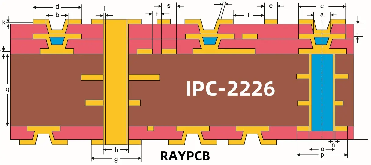
IPC-2226 is a sectional design standard developed by the Institute for Printed Circuits (IPC) specifically for High Density Interconnect (HDI) printed boards. This standard provides guidelines, requirements, and best practices for designing HDI PCBs, which are characterized by their use of microvias, fine lines, and advanced lamination techniques.
Key Objectives of IPC-2226
- Establish common terminology for HDI PCB design
- Define HDI structures and their characteristics
- Provide design guidelines for reliable HDI PCBs
- Ensure consistency in HDI PCB manufacturing processes
- Promote best practices for HDI PCB design and fabrication
Scope of IPC-2226
IPC-2226 covers various aspects of HDI PCB design, including:
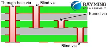
- Microvia structures and types
- Layer stack-up designs
- Material selection considerations
- Design rules for line width and spacing
- Pad and land pattern guidelines
- Testing and reliability requirements
The Importance of IPC-2226 in HDI PCB Design
As HDI technology becomes increasingly prevalent in electronics manufacturing, adherence to IPC-2226 offers several crucial benefits:
1. Standardization
IPC-2226 provides a common language and set of guidelines for HDI PCB design, ensuring consistency across different manufacturers and designers.
2. Reliability
By following IPC-2226 guidelines, designers can create HDI PCBs that meet stringent reliability requirements, crucial for applications in industries such as aerospace, medical devices, and telecommunications.
3. Manufacturability
The standard addresses key manufacturability concerns, helping designers create HDI PCBs that can be produced efficiently and cost-effectively.
4. Performance
IPC-2226 guidelines help optimize HDI PCB designs for electrical performance, addressing issues such as signal integrity and impedance control.
5. Innovation
While providing a framework for HDI PCB design, IPC-2226 also allows for innovation and advancement in HDI technology.
Read more about:
Key Components of IPC-2226
Let’s delve into some of the critical components of the IPC-2226 standard:
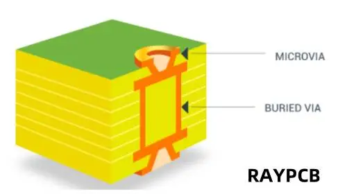
HDI Structure Types
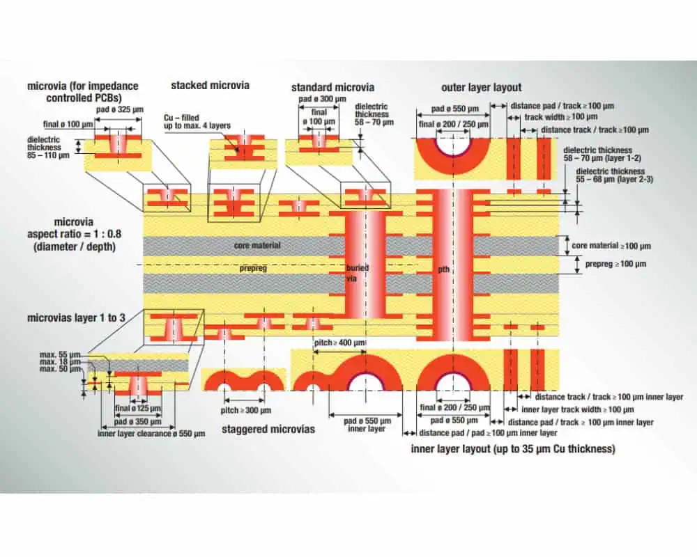
IPC-2226 defines several types of HDI structures, each with its own characteristics and applications:
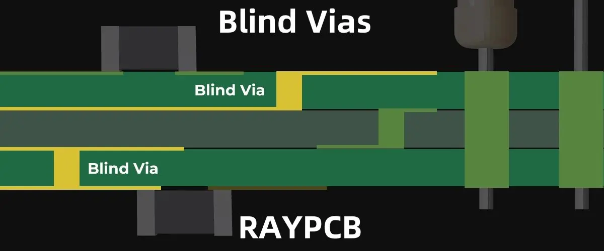
Type I HDI
- Single microvia layer on each side of the core
- Suitable for moderate density requirements
- Relatively simple manufacturing process
Type II HDI
- Multiple microvia layers on each side of the core
- Higher density than Type I
- More complex manufacturing process
Type III HDI
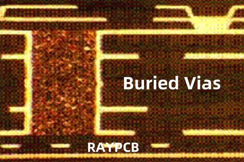
- Microvias that connect three or more layers
- Highest density option
- Most complex manufacturing process
- Subtypes include stacked microvias and staggered microvias
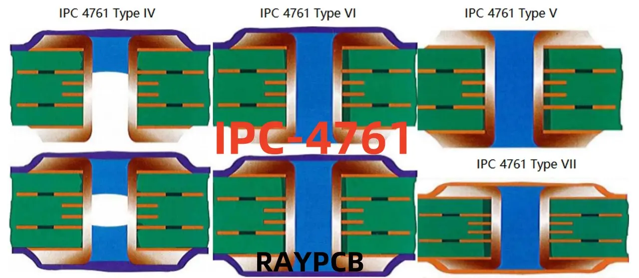
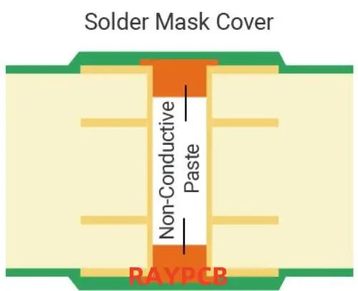
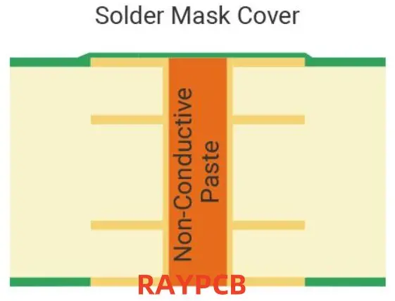
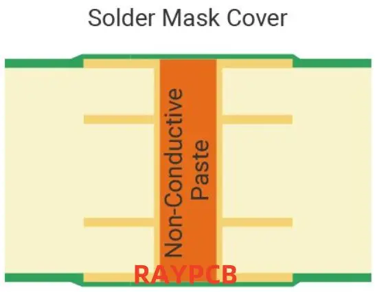
Microvia Definitions and Requirements
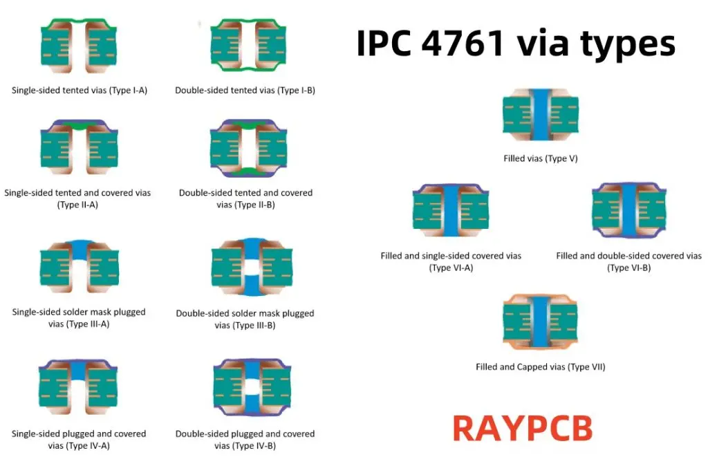
IPC-2226 provides detailed specifications for microvias, including:
- Size definitions (typically ≤150μm in diameter)
- Aspect ratio guidelines
- Plating requirements
- Reliability testing criteria
Layer Stack-Up Design
The standard offers guidelines for designing HDI layer stack-ups, considering factors such as:
- Number of layers
- Microvia types and placement
- Impedance control requirements
- Signal integrity considerations
Material Selection
IPC-2226 addresses the selection of materials for HDI PCBs, taking into account:
- Dielectric materials suitable for laser drilling
- Copper foil types and thicknesses
- Thermal management considerations
- Electrical performance requirements
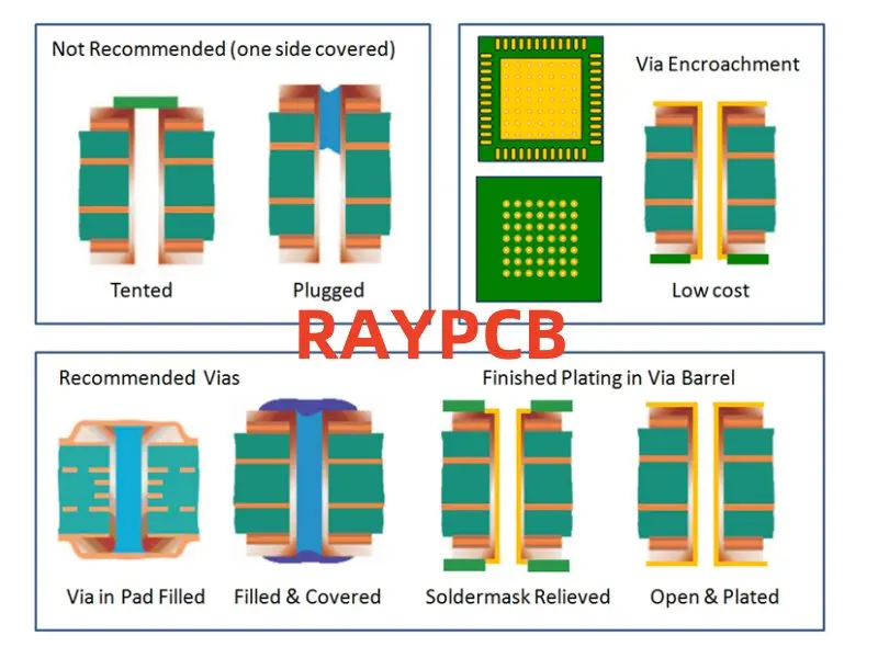
Design Rules
The standard provides specific design rules for HDI PCBs, including:
- Minimum line width and spacing
- Pad and anti-pad sizes
- Microvia land patterns
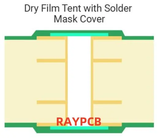
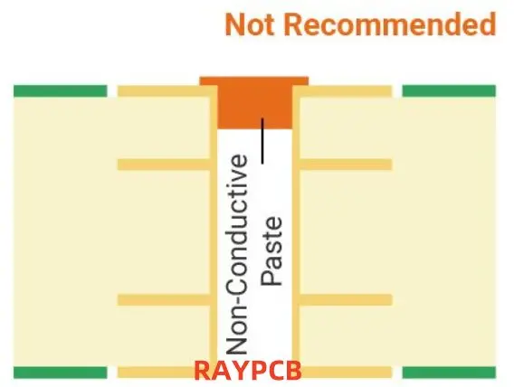
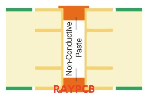
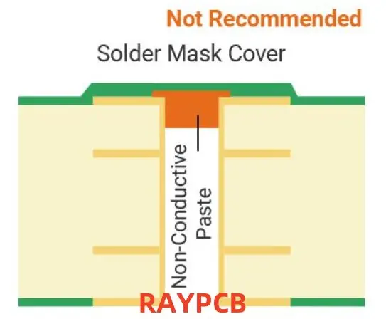
- Solder mask considerations
Implementing IPC-2226 in HDI PCB Design

To effectively implement IPC-2226 in HDI PCB design, consider the following steps:
1. Familiarize Yourself with the Standard
- Obtain a copy of the IPC-2226 document
- Study the terminology and definitions used in the standard
- Understand the different HDI structure types and their applications
2. Assess Your Design Requirements
- Determine the required circuit density
- Evaluate signal integrity and impedance control needs
- Consider thermal management requirements
- Assess reliability expectations based on the intended application
3. Choose the Appropriate HDI Structure
- Select the HDI type (I, II, or III) that best meets your design requirements
- Consider manufacturability and cost implications of different HDI structures
4. Design Your Layer Stack-Up
- Follow IPC-2226 guidelines for layer stack-up design
- Consider signal layer pairing and reference planes
- Optimize for impedance control and signal integrity
5. Apply Design Rules
- Implement IPC-2226 design rules for line width, spacing, and pad sizes
- Adhere to microvia design guidelines, including aspect ratios and land patterns
6. Select Appropriate Materials
- Choose dielectric materials suitable for HDI applications
- Consider copper foil types and thicknesses recommended by IPC-2226
7. Plan for Manufacturability
- Consult with your PCB manufacturer to ensure alignment with IPC-2226 requirements
- Consider design for manufacturing (DFM) guidelines specific to HDI PCBs
8. Implement Reliability Testing
- Follow IPC-2226 recommendations for reliability testing
- Consider additional testing based on your specific application requirements
Challenges in Implementing IPC-2226
While IPC-2226 provides valuable guidelines for HDI PCB design, implementing the standard can present some challenges:
1. Complexity
HDI PCB design is inherently complex, and fully understanding and implementing all aspects of IPC-2226 can be challenging, especially for those new to HDI technology.
2. Balancing Requirements
Designers often need to balance various requirements, such as density, performance, reliability, and cost. Strictly adhering to IPC-2226 may sometimes conflict with other design objectives.
3. Rapid Technological Advancements
As HDI technology continues to evolve rapidly, keeping the standard up-to-date with the latest advancements can be challenging.
4. Manufacturing Capabilities
Not all PCB manufacturers may have the capability to produce HDI boards that meet all IPC-2226 requirements, potentially limiting design options.
5. Cost Considerations
Implementing some aspects of IPC-2226 may increase manufacturing costs, which needs to be balanced against performance and reliability requirements.
Future Trends and IPC-2226
As HDI technology continues to advance, we can expect to see ongoing updates and revisions to IPC-2226. Some potential future trends include:
1. Even Higher Density
Future revisions of IPC-2226 may address even higher density HDI structures, potentially defining new types beyond the current Type III.
2. Advanced Materials
As new materials are developed for HDI applications, IPC-2226 may be updated to include guidelines for their use and implementation.
3. Integration with Other Standards
We may see closer integration between IPC-2226 and other related standards, such as those dealing with flex and rigid-flex circuits or embedded components.
4. Additive Manufacturing
As additive manufacturing techniques become more prevalent in PCB production, IPC-2226 may be updated to address design considerations specific to these processes.
5. Artificial Intelligence and Machine Learning
Future versions of IPC-2226 might incorporate guidelines for using AI and ML in HDI PCB design and verification processes.
Conclusion
IPC-2226 plays a crucial role in standardizing and guiding the design of High Density Interconnect (HDI) printed boards. By providing comprehensive guidelines for HDI structures, materials, design rules, and reliability requirements, this standard helps ensure the production of high-quality, reliable HDI PCBs that meet the demands of modern electronic devices.
As the electronics industry continues to push the boundaries of miniaturization and performance, the importance of standards like IPC-2226 will only grow. Designers and manufacturers who familiarize themselves with this standard and implement its guidelines will be well-positioned to create cutting-edge HDI PCBs that meet the evolving needs of the market.
While implementing IPC-2226 can present challenges, the benefits in terms of standardization, reliability, and manufacturability make it an essential tool in the HDI PCB design process. As technology advances, we can expect IPC-2226 to evolve alongside it, continuing to provide valuable guidance for the next generation of HDI PCBs.
By staying informed about updates to IPC-2226 and related standards, PCB designers and manufacturers can ensure they remain at the forefront of HDI technology, creating innovative and reliable electronic products that push the boundaries of what’s possible in modern electronics.