RO4535 Material Properties: Low Insertion Loss and Enhanced Thermal Stability for High-Frequency Circuits

In the ever-evolving world of high-frequency circuit design, engineers are constantly seeking materials that can meet the demanding requirements of modern applications. One such material that has gained significant attention is RO4535. This advanced laminate offers a unique combination of low insertion loss and enhanced thermal stability, making it an ideal choice for high-frequency circuits. In this comprehensive article, we’ll delve into the properties of RO4535 and explore how it’s revolutionizing the field of RF and microwave circuit design.

Understanding RO4535: A Game-Changer in High-Frequency Circuit Materials

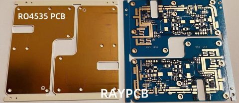
RO4535 is a high-performance laminate material developed by Rogers Corporation, a leader in engineered materials for advanced electronics. This innovative material has been specifically designed to address the challenges faced by engineers working with high-frequency circuits, particularly in applications where low loss and thermal stability are crucial.

What Sets RO4535 Apart?

RO4535 stands out from other materials in its class due to its exceptional combination of properties:

  1. Low insertion loss
  2. Enhanced thermal stability
  3. Consistent electrical performance
  4. Excellent dimensional stability

These characteristics make RO4535 an attractive option for a wide range of high-frequency applications, from telecommunications to aerospace and defense.

Powered By EmbedPress

The Importance of Low Insertion Loss in High-Frequency Circuits

Defining Insertion Loss

Insertion loss refers to the loss of signal power that occurs when a component is inserted into a transmission line or signal path. In high-frequency circuits, minimizing insertion loss is crucial for maintaining signal integrity and overall system performance.

How RO4535 Achieves Low Insertion Loss

RO4535 achieves its low insertion loss through a carefully engineered material composition and manufacturing process. The material’s dielectric constant and loss tangent are optimized to minimize signal attenuation, especially at high frequencies.

Benefits of Low Insertion Loss

  1. Improved signal quality
  2. Reduced power consumption
  3. Extended range for wireless applications
  4. Enhanced overall system efficiency

By utilizing RO4535 in their designs, engineers can create high-frequency circuits that maintain signal integrity over longer distances and operate with greater efficiency.

Read more about:

Enhanced Thermal Stability: A Key Advantage of RO4535

The Challenge of Thermal Management in High-Frequency Circuits

As frequencies increase, so does the heat generated within circuit components. This heat can lead to performance degradation, reliability issues, and even system failure if not properly managed. Thermal stability is therefore a critical consideration in high-frequency circuit design.

RO4535’s Thermal Stability Properties

RO4535 offers exceptional thermal stability, which is crucial for maintaining consistent electrical performance across a wide range of operating temperatures. This stability is achieved through:

  1. Low thermal coefficient of dielectric constant
  2. Low thermal expansion coefficient
  3. High thermal conductivity

Advantages of Enhanced Thermal Stability

  • Consistent electrical performance across temperature ranges
  • Reduced risk of thermal-induced failures
  • Improved reliability in harsh environments
  • Simplified thermal management design

By incorporating RO4535 into their designs, engineers can create high-frequency circuits that perform reliably in a variety of thermal conditions, from extreme cold to high heat.

Applications of RO4535 in High-Frequency Circuits

The unique properties of RO4535 make it suitable for a wide range of applications in the high-frequency domain. Some key areas where this material excels include:

1. 5G and Beyond

As the world moves towards 5G and future wireless technologies, the demand for high-performance materials like RO4535 is increasing. Its low insertion loss and thermal stability make it ideal for:

  • Base station antennas
  • Phased array systems
  • Millimeter-wave circuits

2. Aerospace and Defense

The aerospace and defense sectors require materials that can withstand extreme conditions while maintaining optimal performance. RO4535 finds applications in:

  • Radar systems
  • Electronic warfare equipment
  • Satellite communications

3. Test and Measurement Equipment

Precision is paramount in test and measurement applications. RO4535’s consistent electrical properties make it suitable for:

  • Network analyzers
  • Signal generators
  • High-frequency probes

4. Industrial IoT

As industrial systems become more connected, the need for reliable high-frequency circuits grows. RO4535 can be used in:

  • Industrial sensors
  • Wireless control systems
  • Smart factory infrastructure

Designing with RO4535: Best Practices and Considerations

To fully leverage the benefits of RO4535 in high-frequency circuit design, engineers should keep the following best practices in mind:

1. Impedance Matching

Proper impedance matching is crucial for minimizing reflections and maximizing power transfer. RO4535’s consistent dielectric properties make it easier to achieve and maintain precise impedance matching across a wide frequency range.

2. Thermal Management

While RO4535 offers excellent thermal stability, proper thermal management techniques should still be employed to ensure optimal performance, especially in high-power applications.

3. Manufacturing Processes

RO4535 is compatible with standard PCB manufacturing processes, but care should be taken to follow recommended guidelines for drilling, etching, and lamination to maintain the material’s properties.

4. Simulation and Modeling

Accurate simulation and modeling are essential for high-frequency design. Use the latest material models provided by Rogers Corporation to ensure your simulations accurately reflect RO4535’s behavior.

The Future of High-Frequency Circuit Design with RO4535

As technology continues to advance, the demand for high-performance materials like RO4535 is only expected to grow. The material’s unique combination of low insertion loss and enhanced thermal stability positions it as a key enabler for future innovations in high-frequency circuit design.

Emerging Technologies and RO4535

Looking ahead, RO4535 is likely to play a significant role in emerging technologies such as:

  1. 6G wireless systems
  2. Terahertz communications
  3. Advanced radar and sensing systems
  4. Quantum computing interfaces

By staying at the forefront of material science, RO4535 continues to push the boundaries of what’s possible in high-frequency circuit design.

Conclusion: RO4535 – Enabling the Future of High-Frequency Electronics

In conclusion, RO4535 represents a significant advancement in material technology for high-frequency circuit design. Its low insertion loss and enhanced thermal stability make it an ideal choice for engineers working on cutting-edge applications in telecommunications, aerospace, defense, and beyond.

As we continue to push the limits of what’s possible in high-frequency electronics, materials like RO4535 will play a crucial role in enabling new technologies and improving existing ones. By understanding and leveraging the unique properties of RO4535, engineers can create more efficient, reliable, and high-performing circuits that meet the demanding requirements of modern high-frequency applications.

Whether you’re designing the next generation of 5G infrastructure, developing advanced radar systems, or pushing the boundaries of industrial IoT, RO4535 offers the performance and reliability needed to turn your high-frequency circuit designs into reality.

IPC Standards for PCB Manufacturing: The Complete Quality Assurance Guide

IPCโ€”the Association Connecting Electronics Industriesโ€”sets the global benchmark for PCB design, fabrication, and assembly. These standards provide manufacturers with detailed guidelines on everything from material selection to final inspection, ensuring consistency, reliability, and performance.

The best contract manufacturers (CMs) donโ€™t just follow IPC standardsโ€”they integrate them at every stage of production. Whether itโ€™s IPC-A-600 for acceptability criteria, IPC-6012 for rigid PCB qualification, or J-STD-001 for soldering requirements, top-tier CMs use these standards to:

YouTube video

โœ” Minimize defects โ€“ Reducing rework and scrap costs
โœ” Ensure repeatability โ€“ Delivering consistent quality across production runs
โœ” Meet industry certifications โ€“ Complying with automotive, medical, or military requirements
โœ” Enhance traceability โ€“ Maintaining thorough documentation for audits and troubleshooting

For OEMs, choosing a CM with deep IPC expertise means fewer manufacturing risks and a smoother path to market. In an industry where quality = competitiveness, IPC standards arenโ€™t just guidelinesโ€”theyโ€™re the foundation of success.

What Are IPC Standards?

PCB IPC standards

Definition and Origin

IPC, formerly known as the Institute for Printed Circuits and now as Association Connecting Electronics Industries, is a global trade association that sets the standards for the electronic interconnect industry. IPC standards are a set of guidelines and specifications that cover various aspects of the electronics manufacturing process, including PCB design, production, and quality control.

The Importance of Standardization in PCB Manufacturing

Standardization plays a crucial role in ensuring consistency and quality across the PCB manufacturing industry. By adhering to IPC standards, manufacturers can:

  1. Ensure product reliability
  2. Improve manufacturing efficiency
  3. Enhance product performance
  4. Facilitate better communication between designers, manufacturers, and customers
  5. Reduce production costs by minimizing errors and rework
YouTube video

Key IPC Standards for PCB Manufacturing

IPC-A-600: Acceptability of Printed Boards

IPC-A-600 is one of the most fundamental standards in PCB manufacturing. It sets the criteria for the acceptability of printed circuit boards based on visual inspection. This standard covers:

  • Dimensional requirements
  • Laminate quality
  • Conductor patterns
  • Plated-through holes
  • Surface finishes

The standard defines three classes of PCB quality:

  1. Class 1: General Electronic Products
  2. Class 2: Dedicated Service Electronic Products
  3. Class 3: High-Reliability Electronic Products

Each class has different acceptability criteria, allowing manufacturers to tailor their production to specific product requirements.

IPC-6010 Series: Qualification and Performance Specifications

The IPC-6010 series provides a set of qualification and performance specifications for various types of printed boards. Some key standards in this series include:

  • IPC-6011: Generic Performance Specification for Printed Boards
  • IPC-6012: Qualification and Performance Specification for Rigid Printed Boards
  • IPC-6013: Qualification and Performance Specification for Flexible Printed Boards
  • IPC-6018: Microwave End Product Board Inspection and Test

These standards define the requirements for electrical, mechanical, and environmental performance of PCBs, ensuring that boards meet the necessary quality and reliability standards for their intended applications.

IPC-2220 Series: Design Standards

The IPC-2220 series focuses on PCB design standards, providing guidelines for creating PCB layouts that are both manufacturable and reliable. Key standards in this series include:

  • IPC-2221: Generic Standard on Printed Board Design
  • IPC-2222: Sectional Design Standard for Rigid Organic Printed Boards
  • IPC-2223: Sectional Design Standard for Flexible Printed Boards
  • IPC-2226: Sectional Design Standard for High Density Interconnect (HDI) Printed Boards

These standards cover various aspects of PCB design, including:

  • Layer stackup
  • Conductor spacing and width
  • Via and hole sizes
  • Pad dimensions
  • Thermal management considerations

By following these design standards, engineers can create PCB layouts that are optimized for manufacturability and performance.

IPC-4101: Specification for Base Materials for Rigid and Multilayer Printed Boards

IPC-4101 is crucial for ensuring the quality of the base materials used in PCB manufacturing. This standard defines the requirements for:

  • Laminate and prepreg materials
  • Electrical and mechanical properties
  • Thermal characteristics
  • Environmental durability

Adhering to this standard helps manufacturers select appropriate materials for specific PCB applications, ensuring the final product meets performance and reliability requirements.

IPC-4562: Metal Foil for Printed Board Applications

This standard specifies the requirements for metal foils used in PCB manufacturing, primarily copper foils. It covers:

  • Physical properties of the foil
  • Electrical characteristics
  • Surface treatments
  • Testing methods

Ensuring compliance with IPC-4562 is essential for maintaining consistent quality in the conductive layers of PCBs.

Read more about:

Implementing IPC Standards in PCB Manufacturing

Training and Certification

To effectively implement IPC standards, it’s crucial for personnel involved in PCB manufacturing to receive proper training and certification. IPC offers various certification programs, including:

  1. IPC-A-600 Certified IPC Specialist (CIS)
  2. IPC-6012 Certified IPC Specialist (CIS)
  3. IPC J-STD-001 Certified IPC Trainer (CIT)

These certifications ensure that staff members have a thorough understanding of the relevant standards and can apply them correctly in their work.

Quality Control Processes

Implementing IPC standards requires robust quality control processes throughout the PCB manufacturing workflow. Key elements include:

  1. Incoming Material Inspection: Verifying that all raw materials meet IPC specifications before entering production.
  2. In-Process Inspections: Conducting regular checks during the manufacturing process to catch and correct issues early.
  3. Final Inspection: Thoroughly examining finished PCBs to ensure they meet all applicable IPC standards.
  4. Documentation: Maintaining detailed records of all inspections, tests, and quality control measures.

Equipment and Tools

To meet IPC standards, PCB manufacturers must invest in appropriate equipment and tools. This may include:

  • High-precision measuring instruments
  • Automated optical inspection (AOI) systems
  • X-ray inspection equipment
  • Environmental testing chambers
  • Electrical testing equipment

Regularly calibrating and maintaining this equipment is crucial for ensuring accurate measurements and reliable quality control.

Continuous Improvement

Implementing IPC standards is an ongoing process that requires continuous improvement. Manufacturers should:

  1. Regularly review and update their processes
  2. Stay informed about updates to IPC standards
  3. Conduct internal audits to identify areas for improvement
  4. Encourage feedback from employees and customers
  5. Invest in new technologies that enhance quality control capabilities

Benefits of Adhering to IPC Standards

Enhanced Product Quality and Reliability

By following IPC standards, manufacturers can significantly improve the quality and reliability of their PCBs. This leads to:

  • Reduced failure rates in final products
  • Improved product longevity
  • Enhanced customer satisfaction
  • Fewer warranty claims and returns

Improved Manufacturing Efficiency

Implementing IPC standards can streamline the manufacturing process by:

  • Reducing rework and scrap rates
  • Improving first-pass yields
  • Standardizing processes across different production lines or facilities
  • Facilitating better communication between design and manufacturing teams

Competitive Advantage

Adherence to IPC standards can provide a significant competitive edge in the PCB manufacturing industry:

  • Demonstrating commitment to quality
  • Meeting customer requirements more effectively
  • Qualifying for high-reliability or mission-critical projects
  • Improving reputation in the industry

Global Market Access

Many industries and regions require compliance with IPC standards for electronic components. By adhering to these standards, manufacturers can:

  • Access global markets more easily
  • Meet regulatory requirements in different countries
  • Participate in tenders for government or military contracts

Challenges in Implementing IPC Standards

Cost Considerations

Implementing and maintaining compliance with IPC standards can be costly, involving expenses such as:

  • Training and certification for staff
  • Investment in specialized equipment
  • Potentially slower production speeds due to more rigorous quality control
  • Higher material costs for components that meet IPC specifications

Keeping Up with Standard Updates

IPC regularly updates its standards to keep pace with technological advancements and industry needs. Challenges in this area include:

  • Staying informed about the latest revisions
  • Updating internal processes and documentation
  • Retraining staff on new requirements
  • Potentially upgrading equipment to meet new specifications

Balancing Standards with Innovation

While IPC standards provide crucial guidelines for quality and reliability, they can sometimes be perceived as limiting innovation. Manufacturers must find ways to:

  • Meet standard requirements while still pushing technological boundaries
  • Adapt standards to new materials and manufacturing techniques
  • Participate in the development of new standards to ensure they remain relevant

Future Trends in IPC Standards for PCB Manufacturing

Integration of Industry 4.0 Concepts

As the electronics industry moves towards greater automation and data exchange, future IPC standards are likely to incorporate Industry 4.0 concepts such as:

Addressing Environmental Concerns

With increasing focus on sustainability, future IPC standards may place greater emphasis on:

  • Use of eco-friendly materials in PCB manufacturing
  • Energy-efficient production processes
  • End-of-life considerations and recyclability of PCBs

Adapting to New Technologies

As PCB technology continues to evolve, IPC standards will need to adapt to address:

  • Advanced packaging technologies
  • Flexible and stretchable electronics
  • 3D printed electronics
  • Incorporation of novel materials like graphene

Conclusion

IPC standards play a crucial role in ensuring the quality, reliability, and consistency of PCBs in the ever-evolving electronics manufacturing industry. By providing a common language and set of expectations for designers, manufacturers, and customers, these standards facilitate the production of high-quality electronic components that power our modern world.

While implementing and maintaining compliance with IPC standards presents challenges, the benefits far outweigh the costs. Enhanced product quality, improved manufacturing efficiency, and access to global markets are just a few of the advantages that adherence to these standards can bring.

As technology continues to advance, IPC standards will evolve to address new manufacturing techniques, materials, and industry needs. Staying informed about these changes and actively participating in the standards development process will be crucial for PCB manufacturers who wish to remain competitive in this dynamic industry.

By embracing IPC standards and integrating them into every aspect of the PCB manufacturing process, companies can ensure they are well-positioned to meet the demanding quality requirements of today’s electronic products while preparing for the innovations of tomorrow.

IPC/WHMA-A-620 Standard: The Ultimate Guide to Cable & Wire Harness Acceptance Criteria

In the world of electronics manufacturing, ensuring the quality and reliability of cable and wire harness assemblies is paramount. This is where the IPC/WHMA-A-620 standard comes into play. As a crucial set of guidelines for the industry, it provides comprehensive acceptance criteria for cable and wire harness assemblies. This article will delve deep into the IPC 620 standard, exploring its significance, key components, and how it impacts the electronics manufacturing sector.

Understanding IPC/WHMA-A-620: An Overview

What is IPC/WHMA-A-620?

IPC/WHMA-A-620 is a set of acceptance criteria for cable and wire harness assemblies developed jointly by the IPC (Association Connecting Electronics Industries) and the WHMA (Wire Harness Manufacturer’s Association). This standard provides detailed guidelines for the production and acceptance of cable and wire harness assemblies across various industries, including aerospace, automotive, and consumer electronics.

The Importance of IPC 620 in Electronics Manufacturing

The IPC 620 standard plays a crucial role in ensuring the quality, reliability, and consistency of cable and wire harness assemblies. By providing a common set of acceptance criteria, it helps manufacturers:

  1. Maintain consistent quality standards
  2. Reduce manufacturing defects and rework
  3. Improve product reliability and longevity
  4. Enhance customer satisfaction
  5. Streamline communication between manufacturers and customers

Powered By EmbedPress

Key Components of the IPC/WHMA-A-620 Standard

1. Classes of Products

The IPC 620 standard recognizes that different applications require varying levels of performance, reliability, and quality. To address this, it defines three classes of products:

Class 1: General Electronic Products

These are products where the major requirement is the function of the completed assembly. Examples include consumer electronics and some business equipment.

Class 2: Dedicated Service Electronic Products

This class includes products where continued performance and extended life are required, and for which uninterrupted service is desired but not critical. Examples include communications equipment and sophisticated business machines.

Class 3: High-Performance Electronic Products

These are products where continued high performance or performance-on-demand is critical. Equipment downtime cannot be tolerated, and the end-use environment may be uncommonly harsh. Examples include life support systems and critical aerospace equipment.

2. Acceptance Criteria Categories

The IPC 620 standard covers a wide range of acceptance criteria for various aspects of cable and wire harness assemblies. Some of the key categories include:

Wire and Cable Preparation

This section covers guidelines for:

  • Proper stripping of wire insulation
  • Acceptable levels of conductor damage
  • Correct wire cutting and tinning techniques

Soldered Connections

The standard provides detailed criteria for:

  • Solder joint appearance
  • Acceptable solder quantities
  • Proper wetting of solder joints

Crimped Connections

This category includes guidelines for:

  • Proper crimp height and width
  • Acceptable levels of conductor deformation
  • Correct positioning of conductors in crimp barrels

Connector Assembly

The IPC 620 standard covers:

  • Proper seating of contacts in connectors
  • Acceptable levels of damage to connector housings
  • Correct assembly of multi-piece connectors

Cable and Harness Securing

This section provides criteria for:

  • Proper use of cable ties and clamps
  • Acceptable routing and bundling techniques
  • Correct strain relief methods

Implementing IPC/WHMA-A-620 in Your Manufacturing Process

Training and Certification

To effectively implement the IPC 620 standard, it’s crucial to have properly trained personnel. The IPC offers various levels of training and certification:

  1. Certified IPC Specialist (CIS): For operators and inspectors
  2. Certified IPC Trainer (CIT): For in-house trainers
  3. Master IPC Trainer (MIT): For those who train CITs

Investing in proper training ensures that your team understands and can correctly apply the IPC 620 standard in day-to-day operations.

Quality Control and Inspection

Implementing robust quality control processes based on the IPC 620 standard is essential. This includes:

  1. Developing clear inspection checklists
  2. Establishing acceptance and rejection criteria
  3. Implementing regular audits and reviews
  4. Using appropriate inspection tools and equipment

Documentation and Traceability

Proper documentation is a key aspect of compliance with the IPC 620 standard. This includes:

  1. Maintaining detailed work instructions
  2. Keeping records of inspections and test results
  3. Implementing a system for traceability of materials and processes
  4. Regularly updating documentation to reflect the latest revision of the standard

Read more about:

Benefits of Adhering to IPC/WHMA-A-620

1. Improved Product Quality

By following the detailed acceptance criteria outlined in the IPC 620 standard, manufacturers can significantly improve the quality of their cable and wire harness assemblies. This leads to:

  • Reduced defect rates
  • Improved product performance
  • Enhanced reliability and longevity of assemblies

2. Cost Reduction

While implementing the IPC 620 standard may require initial investment, it can lead to significant cost savings in the long run through:

  • Reduced rework and scrap
  • Fewer field failures and warranty claims
  • Improved efficiency in manufacturing processes

3. Enhanced Customer Satisfaction

Adhering to the IPC 620 standard can greatly improve customer satisfaction by:

  • Meeting or exceeding customer expectations for quality
  • Providing consistent, high-quality products
  • Reducing product failures and returns

4. Competitive Advantage

Companies that fully implement and comply with the IPC 620 standard can gain a competitive edge in the market by:

  • Demonstrating commitment to quality
  • Meeting stringent requirements for high-reliability applications
  • Qualifying for contracts that require IPC 620 compliance

Challenges in Implementing IPC/WHMA-A-620

While the benefits of implementing the IPC 620 standard are clear, there are some challenges that manufacturers may face:

1. Initial Cost and Resource Allocation

Implementing the standard may require:

  • Investment in training and certification
  • Upgrading equipment and tools
  • Allocating resources for documentation and process changes

2. Resistance to Change

Employees may resist changes to established processes. Overcoming this requires:

  • Clear communication of the benefits
  • Proper training and support
  • Gradual implementation of changes

3. Maintaining Compliance

Staying compliant with the IPC 620 standard requires ongoing effort, including:

  • Regular training and recertification
  • Continuous process improvement
  • Keeping up with revisions to the standard

Future Trends and Updates to IPC/WHMA-A-620

The IPC 620 standard is regularly reviewed and updated to keep pace with technological advancements and industry needs. Some areas of focus for future updates may include:

1. Emerging Technologies

As new technologies emerge in cable and wire harness manufacturing, the standard will need to evolve to address:

  • New materials and processes
  • Advanced automation techniques
  • Miniaturization trends in electronics

2. Environmental Considerations

Future revisions may place greater emphasis on:

  • Eco-friendly materials and processes
  • Energy efficiency in manufacturing
  • End-of-life considerations for cable and wire harness assemblies

3. Integration with Industry 4.0

As the industry moves towards smart manufacturing, the IPC 620 standard may need to address:

  • Integration with digital manufacturing systems
  • Real-time quality monitoring and control
  • Data-driven process optimization

Conclusion: The Enduring Importance of IPC/WHMA-A-620

The IPC/WHMA-A-620 standard remains a cornerstone of quality assurance in the cable and wire harness industry. Its comprehensive guidelines and acceptance criteria continue to shape manufacturing practices, ensuring the production of high-quality, reliable assemblies across various sectors.

As technology advances and industry needs evolve, the IPC 620 standard will undoubtedly continue to adapt. However, its fundamental principles of quality, reliability, and consistency will remain crucial for manufacturers striving to produce top-tier cable and wire harness assemblies.

By embracing and implementing the IPC 620 standard, manufacturers can not only improve their products and processes but also position themselves as leaders in quality and reliability in the competitive electronics manufacturing landscape. As we look to the future, the IPC/WHMA-A-620 standard will continue to play a vital role in driving innovation, quality, and excellence in the industry.

How to Remove Solder from PCB: A Comprehensive Guide

Introduction

In the world of electronics repair and modification, knowing how to remove solder from a Printed Circuit Board (PCB) is an essential skill. Whether you’re replacing a faulty component, modifying a circuit, or salvaging parts, mastering the art of desoldering can save you time, money, and frustration.

Why Removing Solder Matters

Removing solder from a PCB is crucial for several reasons:

  • Component replacement: When a component fails, it needs to be removed and replaced.
  • Circuit modification: Desoldering allows for circuit modifications and upgrades.
  • PCB repair: Removing solder is often the first step in repairing damaged traces or pads.
  • Parts salvage: Desoldering lets you recover valuable components from old or discarded boards.
YouTube video

Challenges in Removing Solder

Desoldering isn’t always straightforward. Some common challenges include:

  • Risk of damaging the PCB or nearby components
  • Dealing with lead-free solder, which has a higher melting point
  • Removing solder from multi-layer boards or plated through-holes
  • Working with small or densely packed components

Tools Preview

Before diving into the methods, let’s preview the essential tools for removing solder:

Each tool has its strengths and is suited for different desoldering scenarios.

Essential Tools for Removing Solder

Having the right tools is crucial for effective and safe solder removal. Let’s explore each tool in detail:

1 Desoldering Pump (Solder Sucker)

A desoldering pump, also known as a solder sucker, is a mechanical device that creates suction to remove molten solder.

  • How it works: The pump is primed, then released over melted solder to suck it up.
  • Pros: Effective for through-hole components and larger solder joints.
  • Cons: Can be less effective on surface-mount devices (SMDs) or small joints.

2 Desoldering Braid (Wick)

Desoldering braid, or solder wick, is a fine copper mesh that absorbs molten solder through capillary action.

  • How it works: The braid is placed on the solder joint and heated, drawing the molten solder into itself.
  • Pros: Excellent for surface-mount components and cleaning up residual solder.
  • Cons: Can be less effective on large amounts of solder.

3 Soldering Iron

A soldering iron is essential for heating solder to its melting point.

  • Features to look for: Temperature control, various tip sizes, and a comfortable grip.
  • Tip: Use a clean, well-tinned tip for efficient heat transfer.

4 Hot Air Rework Station

A hot air rework station uses a stream of hot air to melt solder, making it ideal for SMD removal.

  • Advantages: Can heat multiple pins simultaneously, reducing the risk of board damage.
  • Caution: Requires practice to avoid overheating components or the PCB.

5 Flux

Flux is a chemical cleaning agent that improves solder flow and helps in the removal process.

  • Types: Rosin-based, no-clean, and water-soluble fluxes are common.
  • Application: Can be applied as a liquid, paste, or in pen form.

6 Tweezers & Heat Sinks

Tweezers help manipulate small components, while heat sinks protect sensitive parts from excessive heat.

  • Tweezers: ESD-safe tweezers are recommended to prevent static damage.
  • Heat sinks: Clip-on heat sinks can be attached to component leads to dissipate heat.
YouTube video

Method 1: Using a Desoldering Pump

The desoldering pump is a popular and effective tool for removing solder, especially from through-hole components.

Step 1: Prep the PCB

  • Clean the area around the solder joint with isopropyl alcohol.
  • Secure the PCB in a vise or PCB holder to keep it stable.

Step 2: Heat the Solder Joint

  • Set your soldering iron to the appropriate temperature (usually around 315-370ยฐC or 600-700ยฐF).
  • Apply the iron tip to the solder joint until the solder becomes molten.

Step 3: Apply Suction

  • Quickly position the nozzle of the primed desoldering pump over the molten solder.
  • Trigger the pump to create suction and remove the solder.

Step 4: Repeat if Necessary

  • If residual solder remains, reheat the joint and repeat the suction process.
  • For stubborn solder, adding fresh solder can help improve heat transfer and removal.

Step 5: Clean the Pad

  • Use isopropyl alcohol and a lint-free cloth to clean the pad after desoldering.
  • Inspect the pad for any damage or remaining solder.

Pro Tip: Use a heat sink on nearby sensitive components to prevent heat damage during the desoldering process.

YouTube video

Method 2: Using a Desoldering Braid

Desoldering braid is excellent for removing solder from surface-mount components and cleaning up excess solder.

Step 1: Select the Right Braid Width

  • Choose a braid width that matches or slightly exceeds the size of the solder pad.
  • Wider braids are better for larger joints, while narrower ones work well for delicate work.

Step 2: Apply Flux

  • Apply a small amount of flux to the braid to improve its solder-absorbing capacity.
  • Flux also helps in heat transfer and prevents oxidation.

Step 3: Position and Heat

  • Place the braid over the solder joint.
  • Press down gently with a hot soldering iron tip on top of the braid.

Step 4: Allow Solder Absorption

  • As the solder melts, it will be drawn into the braid through capillary action.
  • Once the solder is absorbed, lift both the iron and the braid away from the board.

Step 5: Trim Used Sections

  • Cut off the used portion of the braid to expose fresh copper for the next joint.
  • This ensures maximum efficiency in solder removal.

Warning: Avoid applying excessive heat, as this can cause pad lifting or damage to the PCB.

Read more about:

Method 3: Advanced Techniques

For more complex desoldering tasks, advanced techniques and tools may be necessary.

1 Hot Air Rework Station

Hot air rework stations are ideal for removing surface-mount components with multiple pins.

  • Process:
    1. Apply flux to all pins of the component.
    2. Set the hot air temperature (typically 315-370ยฐC or 600-700ยฐF) and airflow.
    3. Move the hot air nozzle in a circular motion over the component.
    4. Once all solder joints are molten, carefully remove the component with tweezers.
  • Advantages:
    • Reduces the risk of pad damage compared to individual pin desoldering.
    • Ideal for BGA (Ball Grid Array) and QFP (Quad Flat Package) components.

2 Low-Temp Solder Alloy

Low-temperature solder alloys can be used to remove components with less heat exposure.

  • Process:
    1. Apply low-temp solder to all joints of the component.
    2. Heat the joints until all solder is molten.
    3. Remove the component while the solder is liquid.
  • Benefits:
    • Reduces the risk of thermal damage to sensitive components.
    • Useful for working with heat-sensitive parts or multi-layer PCBs.

3 Manual Tools

For certain applications, specialized manual tools can be effective:

  • Desoldering tweezers: Heated tweezers that melt solder on both sides of a component simultaneously.
  • Spring-loaded desoldering irons: Combine a soldering iron with a built-in suction mechanism.

Special Cases & Troubleshooting

1 Removing Solder from Holes

Plated through-holes can be particularly challenging to desolder.

  • Technique:
    1. Use a solder sucker in combination with a soldering iron.
    2. If unsuccessful, try adding fresh solder to improve heat transfer.
    3. For stubborn holes, use a desoldering braid from both sides of the board.

2 Dealing with Stubborn Residue

Sometimes, a thin layer of solder remains after desoldering.

  • Solutions:
    • Use flux and a fine-tipped soldering iron to re-melt and remove the residue.
    • Try a fiberglass brush pen to gently scrub away remaining solder.

3 Removing Solder Without an Iron

In emergencies, solder can be removed without specialized tools:

  • Methods:
    • Use a lighter to heat the solder and quickly tap the board to shake off molten solder.
    • For through-hole components, heat the solder and use a paperclip or pin to push through the hole.

Caution: These methods carry a high risk of board damage and should only be used as a last resort.

Post-Desoldering Cleanup

Proper cleanup after desoldering is crucial for the longevity and reliability of your PCB.

1 Removing Flux Residue

Flux residue can cause corrosion and affect the board’s performance if left uncleaned.

  • Cleaning methods:
    • For rosin-based flux: Use isopropyl alcohol and a soft brush.
    • For no-clean flux: Often doesn’t require cleaning, but can be removed with specialized solvents if necessary.
    • For water-soluble flux: Clean with warm water and a soft brush, then dry thoroughly.

2 Inspection

After cleaning, inspect the board thoroughly:

  • Check for any remaining solder bridges or residue.
  • Examine pads and traces for signs of damage or lifting.
  • Use a magnifying glass or microscope for detailed inspection of small components.

3 Preventing Oxidation

Exposed copper can quickly oxidize, making future soldering difficult.

  • Protection methods:
    • Apply a thin layer of solder (tinning) to exposed pads.
    • Use a PCB lacquer spray to protect the entire board if it won’t be immediately reused.

Frequently Asked Questions

1 Can solder be completely removed from a PCB?

While it’s challenging to remove 100% of the solder, with proper techniques and tools, you can remove enough solder for successful component replacement or board modification.

2 How can I remove solder without a wick or pump?

In a pinch, you can use aluminum foil as a makeshift wick. Place a small strip of foil on the joint, apply the soldering iron, and the foil will absorb the molten solder.

3 How do I remove solder from speaker terminals or through-hole pins?

For large terminals or pins, heat the solder and use pliers to gently wiggle and pull the component while the solder is molten. Be careful not to apply too much force, which could damage the board.

Safety & Best Practices

1 Ventilation

Always work in a well-ventilated area to avoid inhaling solder fumes.

  • Use a fume extractor if working indoors.
  • Consider wearing a mask designed for soldering work.

2 ESD Protection

Electrostatic discharge can damage sensitive components.

  • Use an ESD-safe workstation with a grounded mat and wrist strap.
  • Handle components and boards by their edges to minimize static risk.

3 Temperature Control

Proper temperature control is crucial for effective desoldering and component protection.

  • Start with lower temperatures and increase as needed.
  • Allow components and the board to cool between desoldering attempts.
  • Use heat sinks on nearby components to prevent collateral heat damage.

Conclusion

Mastering the art of removing solder from PCBs is a valuable skill in electronics repair and modification. By understanding the various tools and techniques available, you can tackle a wide range of desoldering challenges safely and effectively.

Remember that practice makes perfect. Start with simpler projects and work your way up to more complex boards. Always prioritize safety, use the right tools for the job, and take your time to avoid damaging valuable components or PCBs.

Whether you’re a hobbyist tinkering with electronics or a professional repairing high-end equipment, the ability to cleanly and efficiently remove solder will serve you well in your electronic endeavors. Happy desoldering!

What is Taiyo PSR 4000 Solder Mask?

Introduction to Taiyo PSR 4000

Taiyo PSR 4000 is a high-performance liquid photoimageable solder mask widely used in the printed circuit board (PCB) manufacturing industry. Developed by Taiyo Ink Manufacturing Co., Ltd., a leading company in the field of solder mask technology, the PSR 4000 series has gained significant popularity due to its exceptional properties and versatility in various PCB applications.

In this comprehensive guide, we’ll explore the characteristics, applications, and benefits of Taiyo PSR 4000 solder mask, providing valuable insights for PCB manufacturers, engineers, and electronics enthusiasts.

Understanding Solder Masks

Before diving deep into Taiyo PSR 4000, let’s briefly discuss what a solder mask is and its importance in PCB manufacturing.

What is a Solder Mask?

A solder mask is a thin layer of polymer applied to the copper traces of a printed circuit board. Its primary functions are:

  1. To protect the copper traces from oxidation
  2. To prevent solder bridges between closely spaced solder pads
  3. To improve the board’s appearance and readability
  4. To protect the board from environmental factors

Types of Solder Masks

There are several types of solder masks available in the market:

  1. Liquid Photoimageable (LPI) solder masks
  2. Dry Film solder masks
  3. Epoxy-based solder masks

Taiyo PSR 4000 falls under the category of Liquid Photoimageable (LPI) solder masks, which are known for their high resolution and excellent performance.

Powered By EmbedPress

Taiyo PSR 4000: Features and Characteristics

Taiyo PSR 4000 stands out among other solder masks due to its unique features and exceptional characteristics. Let’s explore what makes this product a preferred choice for many PCB manufacturers.

Key Features of Taiyo PSR 4000

  1. High Resolution: Taiyo PSR 4000 offers excellent resolution, allowing for fine line definition and small dam formation.
  2. Excellent Chemical Resistance: The mask provides superior resistance against various chemicals used in PCB manufacturing processes.
  3. Thermal Stability: It exhibits good thermal resistance, making it suitable for high-temperature applications.
  4. Fast Curing: The PSR 4000 series features rapid curing times, enhancing production efficiency.
  5. Low Odor: Compared to conventional solder masks, Taiyo PSR 4000 has a significantly reduced odor, improving working conditions.
  6. Environmental Friendliness: The product is formulated to be more environmentally friendly, aligning with global sustainability efforts.

Technical Specifications

To better understand the capabilities of Taiyo PSR 4000, let’s look at some of its technical specifications:

  • Color: Available in various colors, including green, black, red, and blue
  • Solid Content: Typically around 75% (ยฑ2%)
  • Viscosity: Approximately 150-250 dPaยทs (25ยฐC)
  • Exposure Energy: 300-500 mJ/cmยฒ
  • Resolution: Can achieve fine lines down to 50 ฮผm
  • Hardness: Pencil hardness of 6H or higher after curing

Read more about:

Applications of Taiyo PSR 4000

Taiyo PSR 4000 solder mask finds applications in a wide range of PCB manufacturing scenarios. Its versatility and high performance make it suitable for various industries and product types.

Common Applications

  1. Consumer Electronics: Smartphones, tablets, laptops, and other portable devices
  2. Automotive Electronics: Engine control units, infotainment systems, and advanced driver-assistance systems (ADAS)
  3. Industrial Control Systems: PLCs, HMIs, and other industrial automation equipment
  4. Aerospace and Defense: Avionics, communication systems, and military-grade electronics
  5. Medical Devices: Patient monitoring systems, diagnostic equipment, and implantable devices
  6. Telecommunications: Routers, switches, and cellular base stations

Specialized Applications

  1. High-Density Interconnect (HDI) Boards: Taiyo PSR 4000’s high resolution makes it ideal for HDI PCBs with fine lines and small vias.
  2. Flexible and Rigid-Flex PCBs: The mask’s flexibility and adhesion properties make it suitable for flexible circuit applications.
  3. High-Frequency PCBs: Its low dielectric constant and loss tangent make it appropriate for RF and microwave applications.
  4. LED Lighting: The mask’s reflective properties can be utilized in LED PCB manufacturing to enhance light output.

Benefits of Using Taiyo PSR 4000

Implementing Taiyo PSR 4000 in PCB manufacturing processes offers numerous advantages. Let’s explore the key benefits that make this solder mask a popular choice among manufacturers.

1. Enhanced PCB Quality

Taiyo PSR 4000’s high resolution and excellent chemical resistance contribute to improved overall PCB quality. The mask’s ability to form fine dams and maintain sharp edges results in better solder mask definition, reducing the risk of solder bridges and other defects.

2. Increased Production Efficiency

The fast curing time of Taiyo PSR 4000 allows for quicker processing, reducing overall production time. This increased efficiency can lead to higher throughput and improved productivity in PCB manufacturing facilities.

3. Improved Thermal Performance

With its excellent thermal stability, Taiyo PSR 4000 helps protect PCBs from heat-related issues during soldering processes and in high-temperature operating environments. This characteristic is particularly valuable in automotive and industrial applications where thermal management is critical.

4. Environmental and Health Considerations

The low-odor formulation of Taiyo PSR 4000 contributes to a more pleasant working environment for PCB manufacturing staff. Additionally, its environmentally friendly composition aligns with global efforts to reduce the use of harmful chemicals in electronics production.

5. Versatility in Applications

The wide range of applications supported by Taiyo PSR 4000 makes it a versatile choice for PCB manufacturers. Its ability to perform well in various scenarios, from consumer electronics to aerospace applications, reduces the need for multiple solder mask types in production facilities.

Best Practices for Using Taiyo PSR 4000

To maximize the benefits of Taiyo PSR 4000 solder mask, it’s essential to follow best practices during the application and curing processes. Here are some tips for optimal results:

1. Proper Surface Preparation

Ensure that the PCB surface is clean and free from contaminants before applying the solder mask. Proper cleaning and microetching can improve adhesion and overall mask performance.

2. Controlled Application

Use appropriate equipment and techniques to apply the solder mask evenly. Screen printing or spray coating methods are commonly used, depending on the PCB design and production requirements.

3. Optimal Exposure and Development

Follow the recommended exposure energy and development parameters provided by Taiyo. Fine-tuning these parameters based on your specific equipment and requirements can help achieve the best results.

4. Adequate Curing

Ensure proper curing of the solder mask by following the recommended temperature and time profiles. Incomplete curing can lead to reduced performance and reliability issues.

5. Regular Maintenance

Maintain and clean the application equipment regularly to ensure consistent quality in solder mask application.

Conclusion

Taiyo PSR 4000 solder mask has established itself as a high-performance solution in the PCB manufacturing industry. Its exceptional features, including high resolution, excellent chemical resistance, and thermal stability, make it an ideal choice for a wide range of applications, from consumer electronics to aerospace and defense.

By implementing Taiyo PSR 4000 in their production processes, PCB manufacturers can benefit from enhanced board quality, increased efficiency, and improved thermal performance. The mask’s versatility and environmentally friendly formulation further contribute to its popularity in the industry.

As the electronics industry continues to evolve, with increasing demands for miniaturization and higher performance, solder mask technologies like Taiyo PSR 4000 will play a crucial role in meeting these challenges. By staying informed about the latest developments in solder mask technology and following best practices in application and curing, PCB manufacturers can ensure they deliver high-quality, reliable products to meet the needs of various industries.

IPC-SM-840 Explained: Qualification & Performance Standards for Permanent Solder Mask

Introduction

In the world of printed circuit board (PCB) manufacturing, ensuring the quality and reliability of components is paramount. One crucial element in PCB production is the solder mask, a thin layer of polymer applied to the copper traces of a PCB to protect against oxidation and to prevent solder bridges from forming between closely spaced solder pads. The IPC-SM-840 standard plays a vital role in defining the qualification and performance requirements for permanent solder mask used in PCB manufacturing. This article will delve into the intricacies of IPC-SM-840, exploring its significance, key requirements, and impact on the electronics industry.

What is IPC-SM-840?

Definition and Purpose

IPC-SM-840 is a standard developed by the Association Connecting Electronics Industries (IPC) that specifies the qualification and performance requirements for permanent solder mask materials used in the production of printed circuit boards. This standard ensures that solder masks meet specific criteria for durability, resistance to environmental factors, and compatibility with various manufacturing processes.

Scope of the Standard

The IPC-SM-840 standard covers a wide range of aspects related to solder mask performance, including:

  1. Physical properties
  2. Chemical resistance
  3. Electrical properties
  4. Environmental performance
  5. Marking permanence
  6. Coating quality

Importance in the PCB Industry

IPC-SM-840 serves as a crucial benchmark for solder mask quality in the PCB industry. It provides manufacturers, suppliers, and end-users with a common set of expectations and requirements, ensuring consistency and reliability across different products and manufacturers.

Powered By EmbedPress

Key Requirements of IPC-SM-840

The IPC-SM-840 standard outlines several key requirements that solder masks must meet to be considered compliant. Let’s explore these requirements in detail.

Physical Properties

Appearance

The solder mask must have a uniform appearance without blisters, scratches, or other visible defects that could impact its performance or the board’s aesthetics.

Thickness

The standard specifies minimum thickness requirements for the solder mask, ensuring adequate coverage and protection of the underlying copper traces.

Adhesion

Solder masks must demonstrate strong adhesion to the PCB substrate to prevent peeling or flaking during manufacturing processes or product use.

Chemical Resistance

Flux Resistance

The solder mask must withstand exposure to common flux materials used in PCB assembly without degradation.

Solvent Resistance

IPC-SM-840 requires solder masks to resist various solvents that may be encountered during manufacturing or cleaning processes.

Hydrolytic Stability

The standard includes tests for the solder mask’s ability to maintain its properties when exposed to moisture and elevated temperatures.

Electrical Properties

Surface Insulation Resistance (SIR)

Solder masks must maintain high surface insulation resistance to prevent current leakage between conductors.

Dielectric Withstanding Voltage

The standard specifies requirements for the solder mask’s ability to withstand high voltages without breakdown.

Environmental Performance

Thermal Shock Resistance

Solder masks must withstand rapid temperature changes without cracking, peeling, or losing adhesion.

Humidity Resistance

The standard includes tests for the solder mask’s ability to maintain its properties in high-humidity environments.

UV Light Stability

For applications where the PCB may be exposed to sunlight or UV radiation, the solder mask must demonstrate resistance to degradation from UV exposure.

Marking Permanence

Legend Ink Adhesion

If legend ink is applied over the solder mask, it must demonstrate adequate adhesion to prevent peeling or smearing.

Resistance to Marking Solvents

The standard includes tests for the solder mask’s ability to resist common solvents used in marking processes.

Coating Quality

Coverage

The solder mask must provide complete and uniform coverage of the areas it’s intended to protect.

Hardness

IPC-SM-840 specifies requirements for the hardness of the cured solder mask to ensure durability and scratch resistance.

Testing and Qualification Procedures

solder mask
solder mask

To ensure compliance with IPC-SM-840, solder masks undergo a rigorous series of tests and qualification procedures. These procedures are designed to evaluate the solder mask’s performance across various criteria.

Sample Preparation

Before testing, samples are prepared according to the manufacturer’s recommended application and curing processes. This ensures that the tests accurately reflect the solder mask’s performance in real-world applications.

Physical Testing

Physical tests include measurements of thickness, adhesion strength, and hardness. These tests often involve specialized equipment such as micrometers, adhesion testers, and durometers.

Chemical Resistance Testing

Samples are exposed to various chemicals, including fluxes, solvents, and cleaning agents, to evaluate their resistance. The solder mask’s appearance and physical properties are assessed before and after exposure.

Electrical Testing

Electrical tests involve measuring surface insulation resistance and dielectric withstanding voltage. These tests often require specialized electrical testing equipment and controlled environmental conditions.

Environmental Stress Testing

Samples are subjected to thermal shock cycles, high humidity, and UV exposure to evaluate their performance under extreme conditions. These tests often involve environmental chambers capable of rapid temperature and humidity changes.

Long-Term Reliability Testing

Some tests in IPC-SM-840 are designed to evaluate the long-term reliability of the solder mask. These may include extended exposure to high temperatures or repetitive thermal cycling.

Read more about:

Revisions and Updates to IPC-SM-840

Like many industry standards, IPC-SM-840 undergoes periodic revisions to keep pace with advancements in technology and manufacturing processes. Understanding these revisions is crucial for staying compliant with the latest requirements.

IPC-SM-840C

Released in 2002, this revision introduced updates to several test methods and requirements, reflecting advancements in solder mask technology and PCB manufacturing processes.

IPC-SM-840D

Published in 2007, this update further refined the standard, incorporating feedback from industry professionals and addressing emerging challenges in PCB production.

IPC-SM-840E

The latest revision, released in 2016, includes updates to align with other IPC standards and incorporates new test methods to address evolving industry needs.

Impact of IPC-SM-840 on the Electronics Industry

Liquid Photo-imageable Solder Mask

The IPC-SM-840 standard has had a significant impact on the electronics industry, influencing both manufacturers and end-users of PCBs.

For Manufacturers

  1. Quality Assurance: The standard provides a clear benchmark for solder mask quality, helping manufacturers ensure consistent product performance.
  2. Process Optimization: By adhering to IPC-SM-840, manufacturers can optimize their production processes to meet or exceed the standard’s requirements.
  3. Competitive Advantage: Compliance with IPC-SM-840 can be a selling point, demonstrating a commitment to quality and reliability.

For End-Users

  1. Reliability: Products using IPC-SM-840 compliant solder masks are more likely to perform reliably in various environmental conditions.
  2. Consistency: The standard ensures a level of consistency across different manufacturers, simplifying the component selection process.
  3. Long-Term Performance: Adherence to IPC-SM-840 helps ensure the long-term durability and performance of PCBs in finished products.

Challenges in Implementing IPC-SM-840

While IPC-SM-840 provides valuable guidelines for solder mask performance, implementing the standard can present challenges for some manufacturers.

Cost Considerations

Meeting all the requirements of IPC-SM-840 may require investments in new equipment, materials, or processes, potentially increasing production costs.

Technical Complexity

Some of the tests specified in IPC-SM-840 are technically complex and may require specialized equipment or expertise to perform accurately.

Balancing Requirements

Manufacturers must often balance the requirements of IPC-SM-840 with other considerations, such as production speed, cost-effectiveness, and compatibility with specific applications.

Future Trends and Developments

As technology continues to evolve, we can expect future revisions of IPC-SM-840 to address emerging challenges and opportunities in PCB manufacturing.

Integration with Other Standards

Future updates may focus on better integration with other IPC standards, creating a more cohesive framework for PCB quality assurance.

Addressing New Technologies

As new PCB technologies emerge, such as flexible and stretchable electronics, IPC-SM-840 may evolve to include requirements specific to these applications.

Environmental Considerations

Future revisions may place greater emphasis on environmental sustainability, potentially including requirements for eco-friendly solder mask materials or processes.

Conclusion

IPC-SM-840 plays a crucial role in ensuring the quality and reliability of solder masks used in PCB manufacturing. By providing a comprehensive set of qualification and performance standards, it helps maintain consistency across the industry and ensures that PCBs can withstand the rigors of various applications and environments.

For manufacturers, adhering to IPC-SM-840 is not just about meeting a set of requirementsโ€”it’s about committing to quality and reliability in PCB production. For end-users, the standard provides assurance that PCBs will perform as expected, even under challenging conditions.

As technology continues to advance, IPC-SM-840 will undoubtedly evolve to address new challenges and opportunities in the world of electronics manufacturing. By staying informed about these standards and their updates, industry professionals can ensure they remain at the forefront of PCB quality and performance.

FAQs

  1. Q: How often is IPC-SM-840 updated? A: While there’s no fixed schedule, major updates have occurred approximately every 5-10 years, with the latest revision (IPC-SM-840E) released in 2016.
  2. Q: Is compliance with IPC-SM-840 mandatory? A: While not legally mandatory, many companies require compliance with IPC-SM-840 as part of their quality assurance processes.
  3. Q: How can I obtain a copy of the IPC-SM-840 standard? A: The standard can be purchased directly from the IPC website or through authorized distributors.
  4. Q: Are there different levels of compliance within IPC-SM-840? A: Yes, the standard typically defines different classes of performance to accommodate various application requirements.
  5. Q: How does IPC-SM-840 relate to other PCB manufacturing standards? A: IPC-SM-840 is part of a larger family of IPC standards that collectively cover various aspects of PCB design, manufacturing, and quality assurance.

Veroboard Soldering: A Complete Guide to Prototyping Circuits Like a Pro

Introduction to Veroboard Soldering

Veroboard soldering is an essential skill for electronics enthusiasts and professionals alike. This versatile prototyping method allows you to create custom circuits quickly and efficiently. In this comprehensive guide, we’ll explore everything you need to know about Veroboard soldering, from the basics to advanced techniques.

What is Veroboard?

Veroboard, also known as stripboard, is a type of prototyping board with copper strips and pre-drilled holes. It’s an excellent alternative to custom-printed circuit boards (PCBs) for small-scale projects and prototypes.

YouTube video

Essential Tools for Veroboard Soldering

Before diving into the soldering process, let’s review the tools you’ll need for successful Veroboard soldering:

  1. Soldering iron (15-30 watts)
  2. Solder (60/40 or lead-free)
  3. Wire cutters
  4. Wire strippers
  5. Small pliers
  6. Desoldering pump or solder wick
  7. Multimeter
  8. Safety glasses
  9. Ventilation fan

Choosing the Right Soldering Iron

For Veroboard soldering, a temperature-controlled soldering iron is ideal. Look for these features:

  • Adjustable temperature (300-400ยฐC range)
  • Fine tip for precise work
  • Comfortable grip for extended use

Read more about:

Preparing Your Veroboard

Proper preparation is key to successful Veroboard soldering. Follow these steps:

1. Planning Your Circuit

  • Sketch your circuit layout on paper
  • Identify component placement and connections
  • Consider the direction of copper strips

2. Cutting the Veroboard

  • Measure the required board size
  • Score the board with a sharp knife
  • Snap the board along the scored line

3. Breaking Tracks

To isolate different parts of your circuit:

  1. Locate the tracks to be broken
  2. Use a drill bit or track cutter tool
  3. Verify breaks with a multimeter

Veroboard Soldering Techniques

Now, let’s dive into the core Veroboard soldering techniques:

1. Component Placement

  • Insert components from the non-copper side
  • Bend leads slightly to hold components in place
  • Ensure proper orientation of polarized components

2. Soldering Components

Follow these steps for each connection:

  1. Heat the copper pad and component lead
  2. Apply solder to the joint, not the iron tip
  3. Remove solder, then the iron
  4. Allow the joint to cool naturally

3. Creating Solder Bridges

To connect non-adjacent tracks:

  1. Apply flux to both tracks
  2. Heat one track and apply solder
  3. Quickly move to the second track
  4. Add more solder to form a bridge

4. Using Wire Links

For longer connections:

  1. Strip both ends of a wire
  2. Insert into appropriate holes
  3. Solder each end to the Veroboard

Advanced Veroboard Soldering Techniques

As you become more comfortable with Veroboard soldering, try these advanced techniques:

1. Double-Sided Veroboard Soldering

  • Use for more complex circuits
  • Carefully plan component placement
  • Create through-hole connections with wire or component leads

2. Integrated Circuit (IC) Soldering

  • Use IC sockets for easy replacement
  • Align pins carefully before soldering
  • Solder corner pins first, then check alignment

3. Surface Mount Device (SMD) Adaptation

  • Create small solder pads on the copper strips
  • Use fine-tipped tweezers for placement
  • Apply solder sparingly to avoid bridges

Common Veroboard Soldering Mistakes and How to Avoid Them

Even experienced makers can make mistakes. Here are some common issues and solutions:

1. Cold Solder Joints

Problem: Dull, grainy-looking joints Solution: Ensure proper heating of both the pad and component lead

2. Solder Bridges

Problem: Unintended connections between adjacent tracks Solution: Use less solder and a finer tip; clean up with solder wick if needed

3. Lifted Tracks

Problem: Copper track separates from the board Solution: Apply heat carefully and avoid overworking joints

4. Component Damage

Problem: Overheating sensitive components Solution: Use heat sinks and limit soldering time

Tips for Successful Veroboard Soldering

Improve your Veroboard soldering skills with these pro tips:

  1. Keep It Clean: Regularly clean your soldering iron tip
  2. Use Flux: Flux improves solder flow and joint quality
  3. Practice on Scrap: Hone your skills on spare Veroboard pieces
  4. Inspect Your Work: Use a magnifying glass to check joints
  5. Be Patient: Take your time, especially on complex circuits

Veroboard Soldering Projects for Beginners

Start with these simple projects to practice your Veroboard soldering skills:

  1. LED Flasher Circuit: Learn timing and component placement
  2. Simple Amplifier: Understand audio circuit layout
  3. Power Supply: Practice voltage regulation techniques

Veroboard vs. Other Prototyping Methods

Let’s compare Veroboard soldering to other prototyping methods:

Veroboard vs. Breadboard

Veroboard:

  • More permanent
  • Allows for compact designs
  • Requires soldering skills

Breadboard:

  • Quick and easy prototyping
  • No soldering required
  • Limited to simpler circuits

Veroboard vs. Custom PCBs

Veroboard:

  • Faster for one-off projects
  • More flexible for modifications
  • Lower initial cost

Custom PCBs:

  • Better for complex circuits
  • More professional appearance
  • Ideal for mass production

Maintaining Your Veroboard Soldering Equipment

Proper maintenance ensures long-lasting, reliable performance:

  1. Clean Your Soldering Iron: Regularly clean and tin the tip
  2. Replace Consumables: Change soldering iron tips and sponges as needed
  3. Store Properly: Keep tools in a dry, clean environment
  4. Calibrate When Necessary: Check temperature settings periodically

Safety Considerations in Veroboard Soldering

Always prioritize safety when Veroboard soldering:

  1. Ventilation: Work in a well-ventilated area to avoid fume inhalation
  2. Eye Protection: Wear safety glasses to protect against solder splatter
  3. Fire Safety: Use a soldering iron stand and keep flammable materials away
  4. First Aid: Keep a first aid kit nearby for minor burns
  5. Proper Disposal: Dispose of waste solder and flux responsibly

Troubleshooting Veroboard Circuits

When your Veroboard circuit doesn’t work as expected:

  1. Visual Inspection: Check for obvious issues like solder bridges or missing connections
  2. Continuity Testing: Use a multimeter to verify connections
  3. Signal Tracing: Follow the signal path to identify where it stops
  4. Component Testing: Verify individual component functionality
  5. Power Supply Check: Ensure proper voltage and current delivery

Advanced Applications of Veroboard Soldering

As your skills improve, explore these advanced applications:

  1. Modular Circuit Design: Create interconnectable circuit blocks
  2. Mixed-Technology Boards: Combine through-hole and surface-mount components
  3. Multi-Layer Designs: Stack Veroboards for complex 3D circuits
  4. Custom Enclosures: Design and build enclosures around your Veroboard circuits

Future Trends in Prototyping and Veroboard Alternatives

While Veroboard remains popular, new prototyping methods are emerging:

  1. 3D-Printed Circuit Boards: Rapid prototyping with conductive filaments
  2. Flexible PCBs: Adaptable circuits for wearable technology
  3. Paper Electronics: Low-cost, disposable circuit prototyping
  4. Modular Prototyping Systems: Pre-made circuit blocks for quick assembly

Conclusion: Mastering Veroboard Soldering

Veroboard soldering is a valuable skill that bridges the gap between breadboard prototypes and custom PCBs. With practice and patience, you can create professional-quality circuits for a wide range of applications. Remember these key points:

  1. Proper preparation is crucial for successful Veroboard projects
  2. Technique matters: focus on creating clean, strong solder joints
  3. Start with simple projects and gradually increase complexity
  4. Always prioritize safety in your workspace
  5. Maintain your tools for consistent performance

Whether you’re a hobbyist or a professional, mastering Veroboard soldering will expand your capabilities in circuit design and prototyping. Keep practicing, stay curious, and don’t be afraid to tackle challenging projects. With time, you’ll be soldering Veroboard circuits like a pro!

Solder Suckers Vs. Desoldering Guns: Which Tool is Right for Your Project?

Soldering is an essential skill in electronics repair, especially when replacing faulty components on a PCB. But before you can solder a new part in place, you must first remove the old oneโ€”making desoldering the critical first step. For most hobbyists and makers, the go-to tool for this job is the humble solder sucker (also known as a desoldering pump), offering a simple yet effective way to clear solder from joints.

Understanding Solder Removal Tools

Before we dive into the comparison, let’s briefly define our two contenders:

What is a Solder Sucker?

A solder sucker, also known as a desoldering pump, is a manual tool used to remove molten solder from a soldered joint. It works by creating a vacuum that sucks up the liquefied solder.

What is a Desoldering Gun?

A desoldering gun is an electrical tool that combines heat to melt the solder and suction to remove it, all in one device. It’s often more powerful and efficient than a manual solder sucker.

YouTube video

Solder Suckers: In-Depth Look

Let’s start by examining solder suckers in detail.

How Solder Suckers Work

  1. Preparation: The spring-loaded piston is compressed and locked in place.
  2. Heating: The solder joint is heated with a separate soldering iron.
  3. Activation: The release button is pressed, creating a strong vacuum.
  4. Suction: The molten solder is quickly drawn into the cylinder.

Types of Solder Suckers

1. Manual Plunger-Style Solder Suckers

  • Most common and affordable
  • Requires manual operation
  • Examples: Engineer SS-02, Tenma 21-8240

2. Vacuum-Style Solder Suckers

  • Uses a rubber bulb to create suction
  • Gentler on delicate components
  • Examples: Edsyn Soldapullt, ZD-180 Vacuum Desoldering Pump

Pros of Using a Solder Sucker

  1. Affordability: Generally much cheaper than desoldering guns
  2. Portability: No power source required, easy to carry
  3. Simplicity: Easy to use with minimal training
  4. Maintenance: Simple to clean and maintain
  5. Precision: Good for targeted, small-scale desoldering tasks

Cons of Using a Solder Sucker

  1. Manual Effort: Requires coordination with a separate soldering iron
  2. Efficiency: Can be time-consuming for large desoldering jobs
  3. Heat Control: Depends on the user’s skill with a soldering iron
  4. Fatigue: Can be tiring for extended use

Read more about:

Desoldering Guns: A Comprehensive Overview

Now, let’s explore desoldering guns and their features.

How Desoldering Guns Work

  1. Heating: An internal heating element melts the solder.
  2. Suction: A motorized vacuum pump removes the molten solder.
  3. Collection: The removed solder is collected in a reservoir or filter.

Types of Desoldering Guns

1. Handheld Desoldering Guns

  • Portable and easy to maneuver
  • Good for field work and repairs
  • Examples: Hakko FR-301, Aoyue 8800 Desoldering Gun

2. Desoldering Stations

  • More powerful, often with temperature control
  • Suitable for professional and heavy-duty use
  • Examples: Hakko FM-204, YIHUA 948-II

Pros of Using a Desoldering Gun

  1. Efficiency: Faster for large desoldering jobs
  2. All-in-One: Combines heating and suction in one tool
  3. Consistent Heat: Often features temperature control
  4. Ergonomics: Designed for prolonged use with less fatigue
  5. Precision: Some models offer fine temperature and suction control

Cons of Using a Desoldering Gun

  1. Cost: Significantly more expensive than solder suckers
  2. Power Requirement: Needs an electrical outlet to operate
  3. Learning Curve: Can be more complex to use effectively
  4. Maintenance: Requires regular cleaning and filter changes
  5. Size and Weight: Generally bulkier and heavier than solder suckers

Comparing Solder Suckers and Desoldering Guns

Now that we’ve examined each tool individually, let’s compare them across various factors to help you decide which is right for your project.

1. Cost Comparison

Solder Suckers:

  • Entry-level: 5โˆ’5โˆ’20
  • Professional-grade: 20โˆ’20โˆ’50

Desoldering Guns:

  • Entry-level: 50โˆ’50โˆ’100
  • Professional-grade: 100โˆ’100โˆ’500+

Winner: Solder suckers are significantly more affordable, making them ideal for hobbyists and occasional users.

2. Ease of Use

Solder Suckers:

  • Simple operation
  • Requires coordination with a separate soldering iron
  • Minimal setup time

Desoldering Guns:

  • All-in-one operation
  • May have a steeper learning curve
  • Requires setup and warm-up time

Winner: Solder suckers are simpler to use, especially for beginners, but desoldering guns offer more convenience once mastered.

3. Efficiency and Speed

Solder Suckers:

  • Slower for large jobs
  • Requires frequent emptying
  • Manual operation can be tiring

Desoldering Guns:

  • Faster for extensive desoldering work
  • Continuous operation possible
  • Less physical effort required

Winner: Desoldering guns are more efficient, especially for larger projects or professional use.

4. Precision and Control

Solder Suckers:

  • Good for targeted, small-scale work
  • Precision depends on user skill
  • Limited control over suction strength

Desoldering Guns:

  • Adjustable temperature and suction on some models
  • Consistent heat application
  • Can be overkill for simple tasks

Winner: Tie. Solder suckers offer good precision for small tasks, while desoldering guns provide better control for complex work.

5. Portability

Solder Suckers:

  • Highly portable
  • No power source required
  • Lightweight and compact

Desoldering Guns:

  • Less portable due to power requirements
  • Heavier and bulkier
  • Some cordless models available, but limited

Winner: Solder suckers are much more portable, making them ideal for field work or tight spaces.

6. Maintenance

Solder Suckers:

  • Easy to disassemble and clean
  • Few or no consumable parts
  • Simple repairs possible

Desoldering Guns:

  • Regular cleaning required
  • Filter and nozzle replacements needed
  • More complex repairs, often requiring professional service

Winner: Solder suckers are easier and cheaper to maintain.

Choosing the Right Tool for Your Project

Now that we’ve compared solder suckers and desoldering guns, let’s look at which tool might be best for different types of projects and users.

For Hobbyists and Occasional Users

Recommended Tool: Solder Sucker

Reasons:

  • More affordable
  • Easier to learn and use
  • Sufficient for most small-scale projects
  • Low maintenance requirements

Best Practices:

  • Invest in a quality solder sucker for better results
  • Practice coordinating with your soldering iron
  • Keep the tip clean for optimal performance

For Professional Technicians and Frequent Users

Recommended Tool: Desoldering Gun

Reasons:

  • More efficient for large-scale work
  • Reduces hand fatigue during extended use
  • Provides consistent heat and suction
  • Often offers better precision for complex boards

Best Practices:

  • Choose a model with adjustable temperature and suction
  • Regularly clean and maintain your desoldering gun
  • Keep spare filters and nozzles on hand

For Mixed Use or Growing Hobbyists

Recommended Tool: Both

Reasons:

  • Solder sucker for simple tasks and portability
  • Desoldering gun for larger projects and efficiency

Best Practices:

  • Start with a quality solder sucker
  • Upgrade to a desoldering gun as skills and projects advance
  • Use each tool for its strengths

Tips for Effective Solder Removal

Regardless of which tool you choose, these tips will help you achieve better results:

  1. Use Flux: Apply flux to improve heat transfer and solder flow
  2. Add Fresh Solder: Sometimes adding a bit of fresh solder helps remove old, oxidized solder
  3. Proper Heat: Ensure the solder is fully melted before attempting removal
  4. Clean Tools: Regularly clean your solder sucker or desoldering gun for optimal performance
  5. Practice: Start with scrap boards to improve your technique
  6. Safety First: Always wear safety glasses and work in a well-ventilated area

Environmental and Safety Considerations

When working with solder removal tools, keep these environmental and safety factors in mind:

Environmental Impact

  • Proper disposal of removed solder (may contain lead)
  • Energy consumption of electric desoldering guns
  • Longevity and repairability of tools

Safety Precautions

  • Use in well-ventilated areas to avoid inhaling fumes
  • Wear safety glasses to protect against solder splatter
  • Be cautious of hot surfaces and components
  • Follow proper electrical safety with desoldering guns

Future Trends in Solder Removal Technology

As we look to the future, several trends are shaping the world of solder removal:

  1. Increased Automation: Robotic desoldering for large-scale operations
  2. Eco-Friendly Solutions: Development of lead-free solder removal techniques
  3. Smart Tools: Integration of IoT and data logging in professional-grade tools
  4. Improved Ergonomics: Focus on reducing user fatigue in both manual and electric tools
  5. Hybrid Tools: Combination of different technologies for more versatile solder removal

Conclusion: Making Your Choice

Choosing between a solder sucker and a desoldering gun ultimately depends on your specific needs, budget, and the types of projects you undertake. Here’s a quick summary to help you decide:

  • Choose a Solder Sucker if:
    • You’re a hobbyist or occasional user
    • You’re on a tight budget
    • You need a portable solution
    • Your projects involve simple, small-scale desoldering
  • Choose a Desoldering Gun if:
    • You frequently work on large desoldering projects
    • You’re a professional or serious hobbyist
    • Efficiency and reduced fatigue are priorities
    • You’re willing to invest in a more powerful tool

Remember, many experienced electronics enthusiasts and professionals keep both tools in their arsenal, using each for its strengths. As you grow in your electronics journey, you may find that having both a reliable solder sucker and a efficient desoldering gun gives you the flexibility to tackle any project that comes your way.

Whichever tool you choose, practice and patience will help you master the art of solder removal, leading to cleaner, more professional results in all your electronics projects.

Complete Guide to STM32H743VIT6: Datasheet, Dev Boards, and Alternatives

The STM32H743VIT6 is a powerful microcontroller that has gained significant popularity in the embedded systems world. This comprehensive guide will delve into its features, applications, and alternatives, providing you with all the information you need to decide if it’s the right choice for your next project.

Understanding the STM32H743VIT6

The STM32H743VIT6 is part of the high-performance STM32H7 series of microcontrollers from STMicroelectronics. It’s designed to meet the demands of advanced embedded applications that require high processing power, real-time capabilities, and a wide range of peripherals.

Key Features of STM32H743VIT6

  1. High-Performance Core: At the heart of the STM32H743VIT6 is an Arm Cortex-M7 core, capable of running at speeds up to 480 MHz.
  2. Extensive Memory: It boasts 2 MB of Flash memory and 1 MB of RAM, providing ample space for complex applications.
  3. Rich Peripheral Set: The microcontroller includes a variety of peripherals such as USB OTG, Ethernet, CAN, and various serial interfaces.
  4. Advanced Graphics Capabilities: With its Chrom-ART Acceleratorโ„ข and JPEG codec, it’s well-suited for graphical applications.
  5. Low Power Modes: Despite its high performance, the STM32H743VIT6 offers several low-power modes for energy-efficient operation.

Diving into the STM32H743VIT6 Datasheet

The datasheet is an essential resource for anyone working with the STM32H743VIT6. Let’s break down some of the most important sections:

Electrical Characteristics

The STM32H743VIT6 operates with a supply voltage range of 1.62V to 3.6V. It can source or sink up to 25 mA per I/O pin, making it suitable for directly driving LEDs and other moderate-current devices.

Memory Organization

The microcontroller’s memory is organized as follows:

  • 2 MB of Flash memory
  • 1 MB of SRAM, including 192 KB of TCM RAM for critical real-time tasks
  • 4 KB of backup SRAM
  • Optional external memory support via FMC

Peripherals

The STM32H743VIT6 is equipped with a wide array of peripherals, including:

  • Multiple timers and watchdogs
  • Up to 35 communication interfaces (including USART, SPI, I2C, and CAN)
  • 3x 12-bit ADCs and 2x 12-bit DACs
  • Random number generator
  • CRC calculation unit

Package Information

The STM32H743VIT6 comes in a 100-pin LQFP package, measuring 14x14mm. This package type offers a good balance between pin count and ease of handling for both prototyping and production.

Development Boards Featuring STM32H743VIT6

Several development boards are available that showcase the capabilities of the STM32H743VIT6. These boards can significantly speed up your development process by providing a ready-to-use platform with additional features.

1. STM32H743I-EVAL

This is STMicroelectronics’ official evaluation board for the STM32H743 series. It’s a feature-rich platform that includes:

  • 4.3″ TFT color LCD
  • Ethernet connector
  • USB OTG ports
  • Audio codec
  • QSPI Flash and SRAM

While it’s one of the more expensive options, it provides a comprehensive set of features for evaluating the full capabilities of the STM32H743VIT6.

2. WeAct Studio Black Pill

For those looking for a more compact and budget-friendly option, the WeAct Studio Black Pill featuring the STM32H743VIT6 is an excellent choice. Key features include:

  • Small form factor (53mm x 20.5mm)
  • USB-C connector
  • SD card slot
  • User LED and button

This board is ideal for projects where space is at a premium or for those just starting with STM32H7 series microcontrollers.

3. Waveshare OpenH743I-C

The Waveshare OpenH743I-C strikes a balance between features and cost. Notable aspects include:

  • On-board ST-LINK/V2-1 programmer/debugger
  • Arduino-compatible headers
  • Multiple expansion interfaces
  • 1.3″ OLED display

This board is well-suited for both beginners and experienced developers who want a versatile platform without breaking the bank.

Programming the STM32H743VIT6

When it comes to programming the STM32H743VIT6, you have several options:

1. STM32CubeIDE

STM32CubeIDE is the official integrated development environment from STMicroelectronics. It provides a comprehensive set of tools for configuring, programming, and debugging STM32 microcontrollers.

2. Keil MDK

Keil MDK is a popular choice for Arm-based microcontrollers. It offers a robust development environment with advanced debugging capabilities.

3. PlatformIO

For those who prefer an open-source solution, PlatformIO is an excellent choice. It integrates with various IDEs and supports a wide range of development boards, including those based on the STM32H743VIT6.

4. Arduino IDE

Yes, you can even use the Arduino IDE with the STM32H743VIT6, thanks to the STM32duino project. While it may not unlock the full potential of the microcontroller, it’s a great option for those familiar with the Arduino ecosystem.

Alternatives to STM32H743VIT6

While the STM32H743VIT6 is a powerful microcontroller, it’s always worth considering alternatives to ensure you’re choosing the best option for your specific needs.

1. NXP i.MX RT1062

The i.MX RT1062 is part of NXP’s crossover MCU family, offering:

  • Arm Cortex-M7 core running at up to 600 MHz
  • 1 MB on-chip RAM
  • Rich set of peripherals including USB, Ethernet, and CAN

It’s a strong contender, especially for applications requiring high processing power and real-time capabilities.

2. Microchip SAMA5D27

For those considering a step up to an application processor, the SAMA5D27 offers:

  • Arm Cortex-A5 core running at up to 500 MHz
  • 128 MB DDR2 memory
  • Linux support

This could be a good choice if your application requires running a full operating system.

3. ESP32-S3

If your project requires built-in Wi-Fi and Bluetooth capabilities, the ESP32-S3 from Espressif Systems is worth considering:

  • Dual-core Xtensa LX7 processor running at up to 240 MHz
  • Wi-Fi and Bluetooth 5 (LE) connectivity
  • Up to 512 KB RAM and 16 MB Flash

While it doesn’t match the raw processing power of the STM32H743VIT6, its integrated wireless capabilities make it an attractive option for IoT applications.

Conclusion: Is the STM32H743VIT6 Right for Your Project?

The STM32H743VIT6 is a powerful and versatile microcontroller that excels in applications requiring high processing power, real-time performance, and a rich set of peripherals. It’s particularly well-suited for projects involving complex signal processing, advanced control systems, or high-resolution graphical interfaces.

However, it may be overkill for simpler projects or those with strict power consumption requirements. In such cases, a less powerful MCU from the STM32 family or an alternative like the ESP32 might be more appropriate.

When choosing a microcontroller, always consider your project’s specific requirements, including processing power, memory needs, peripheral requirements, power consumption, and development ecosystem. The STM32H743VIT6 offers an impressive feature set, but the best choice will always depend on your unique project needs.

What is Copper Filled Via?

Printed circuit boards (PCBs) rely on viasโ€”tiny conductive pathways that transmit signals between layers. During manufacturing, a copper layer is deposited onto the substrate, forming both the conductive traces and the plated through-hole (PTH) walls that interconnect layers. While standard plated vias are sufficient for many applications, advanced designs often demand copper-filled vias for superior performance.

To create a copper-filled via, manufacturers first fill the via with an epoxy resin, then electroplate it with pure copper. This process increases fabrication costs but unlocks unique benefits:

  • Higher current-carrying capacity (reduced resistance vs. hollow or non-copper fills).
  • Improved thermal conductivity, critical for power electronics and high-temperature applications.
  • Enhanced structural integrity, minimizing risks of void formation or cracking during thermal cycling.
YouTube video

Unlike alternative conductive fills (e.g., silver paste), copper-filled vias offer lower impedance and better high-frequency performance, making them ideal for:

  • High-power PCBs (e.g., automotive, industrial).
  • HDI designs requiring microvias.
  • RF/microwave circuits where signal integrity is paramount.

This guide explores the key advantages of copper-filled vias and how to leverage them in your PCB designs.

Understanding Copper Filled Vias

Copper filled vias are a type of plated through-hole (PTH) in a printed circuit board that has been completely filled with copper. Unlike traditional vias that are hollow, copper filled vias are solid, providing a continuous path for electrical signals and heat dissipation.

Key Features of Copper Filled Vias

  • Solid Construction: Filled entirely with copper, eliminating air gaps.
  • Enhanced Conductivity: Offers superior electrical performance compared to hollow vias.
  • Improved Thermal Management: Facilitates better heat dissipation.
  • Increased Reliability: Reduces the risk of via failure due to thermal stress or mechanical strain.

Types of Copper Filled Vias

  1. Through-Hole Copper Filled Vias: Extend through all layers of the PCB.
  2. Blind Copper Filled Vias: Connect an outer layer to one or more inner layers, but not through the entire board.
  3. Buried Copper Filled Vias: Connect inner layers without extending to the outer layers.

Read more about:

Via Filling Process

The process of filling vias with copper or other materials is a critical step in advanced PCB manufacturing. Let’s explore the various methods used for via filling.

1. Conductive Via Filling

Conductive via filling involves using electrically conductive materials to fill the vias. Copper is the most common material used due to its excellent conductivity and compatibility with PCB manufacturing processes.

Process Steps for Copper Filled Vias:

  1. Via Drilling: Creating the initial hole in the PCB.
  2. Cleaning: Removing any debris from the drilling process.
  3. Electroplating: Depositing a thin layer of copper on the via walls.
  4. Copper Filling: Using electroplating or paste filling techniques to completely fill the via with copper.
  5. Planarization: Removing excess copper to create a smooth surface.

2. Non-Conductive Via Filling

Non-conductive via filling uses insulating materials, typically epoxy resins, to fill the vias. This method is often used when electrical conductivity through the via is not required.

Applications of Non-Conductive Filled Vias:

  • Improving board planarity for surface mount assembly.
  • Enhancing the structural integrity of the PCB.
  • Creating a smooth surface for legend printing or solder mask application.

3. Copper-Plated Shut Filled Vias

Copper-plated shut vias are a variation of copper filled vias where the via is gradually plated shut rather than being completely filled.

Characteristics of Copper-Plated Shut Vias:

  • Process: Involves extended electroplating to close the via opening.
  • Structure: Results in a via that is mostly hollow but sealed at both ends.
  • Applications: Used in situations where full copper filling is not necessary but via sealing is required.

4. Epoxy Filled Vias

Epoxy filled vias use a non-conductive epoxy resin to fill the via hole. This method is often used in conjunction with copper plating for specific applications.

Benefits of Epoxy Filled Vias:

  • Cost-Effective: Generally less expensive than full copper filling.
  • Planar Surface: Provides a smooth surface for component mounting.
  • Structural Support: Enhances the mechanical strength of the PCB.

5. Gold Filled Via

Gold filled vias are a specialized type of conductive via filling used in high-reliability applications.

Features of Gold Filled Vias:

  • Superior Conductivity: Gold offers excellent electrical performance.
  • Corrosion Resistance: Gold’s inert nature prevents oxidation and corrosion.
  • High-Reliability Applications: Often used in aerospace and medical devices.

Powered By EmbedPress

Benefits of Copper Filled Vias

Copper filled vias offer numerous advantages over traditional hollow vias, making them increasingly popular in high-performance PCB designs.

1. Enhanced Electrical Performance

  • Lower Resistance: Solid copper provides a more conductive path for electrical signals.
  • Reduced Signal Loss: Minimizes signal degradation in high-frequency applications.
  • Improved Signal Integrity: Reduces electromagnetic interference (EMI) and crosstalk.

2. Superior Thermal Management

  • Efficient Heat Dissipation: Copper’s high thermal conductivity helps in removing heat from components.
  • Thermal Via Applications: Ideal for creating thermal vias under high-power components.

3. Increased Reliability

  • Mechanical Strength: Solid structure improves the overall durability of the PCB.
  • Resistance to Thermal Stress: Better withstands temperature fluctuations and thermal cycling.
  • Reduced Risk of Failure: Eliminates issues related to hollow via failures, such as trapped chemicals or air bubbles.

4. Design Flexibility

  • Higher Current Capacity: Allows for thinner traces while maintaining current-carrying capability.
  • Space Saving: Enables more compact designs by reducing the need for multiple vias.

5. Manufacturing Benefits

  • Improved Yields: Reduces issues related to via plating inconsistencies.
  • Enhanced Planarity: Creates a smoother surface for component mounting and assembly.

Filled Via vs. Plated Through Hole Applications

While copper filled vias and traditional plated through holes (PTHs) serve similar purposes, they have distinct characteristics that make them suitable for different applications.

Copper Filled Vias:

  • High-Density Designs: Ideal for HDI boards where space is at a premium.
  • High-Frequency Applications: Better signal integrity in RF and high-speed digital circuits.
  • Thermal Management: Superior heat dissipation for power electronics.

Plated Through Holes:

  • Cost-Effective: Generally less expensive for simpler board designs.
  • Ease of Manufacturing: Simpler process for basic PCB production.
  • Through-Board Connections: Effective for connecting multiple layers in thicker boards.

Similarities and Differences Between Copper and Epoxy Filled Vias

Understanding the similarities and differences between copper and epoxy filled vias can help in choosing the right option for specific PCB applications.

Similarities:

  • Improved Planarity: Both provide a smooth surface for component mounting.
  • Enhanced Structural Integrity: Increase the overall strength of the PCB.
  • Via Sealing: Both methods effectively seal the via, preventing ingress of contaminants.

Differences:

Copper Filled Vias:

  • Conductivity: Electrically conductive throughout the via.
  • Thermal Performance: Superior heat dissipation.
  • Cost: Generally more expensive due to the copper filling process.

Epoxy Filled Vias:

  • Insulation: Electrically insulating, useful for certain design requirements.
  • Cost: Typically less expensive than copper filling.
  • Thermal Properties: Lower thermal conductivity compared to copper.

Copper Filled Via PCB Applications

Copper filled vias find applications in a wide range of high-performance electronic products and industries.

1. Aerospace and Defense

  • Satellite Communications: High-reliability boards for space applications.
  • Radar Systems: High-frequency PCBs with excellent signal integrity.
  • Avionics: Rugged boards capable of withstanding extreme conditions.

2. Telecommunications

  • 5G Infrastructure: High-speed, high-density boards for network equipment.
  • Optical Networking: PCBs for fiber optic communication systems.

3. Consumer Electronics

  • Smartphones: Compact, multi-layer boards with high component density.
  • Wearable Devices: Thin, flexible PCBs with efficient thermal management.

4. Automotive Electronics

  • Advanced Driver Assistance Systems (ADAS): High-reliability boards for safety-critical applications.
  • Electric Vehicle Control Systems: Power electronics with superior thermal management.

5. Medical Devices

  • Implantable Devices: High-reliability, biocompatible PCBs.
  • Diagnostic Equipment: High-performance boards for medical imaging systems.

6. High-Performance Computing

  • Data Centers: Servers and networking equipment requiring high-speed signal transmission.
  • Artificial Intelligence Hardware: Dense, high-performance boards for AI accelerators.

Conclusion: The Future of Copper Filled Vias in PCB Technology

As the electronics industry continues to push the boundaries of performance and miniaturization, copper filled vias will play an increasingly crucial role in PCB design and manufacturing. Their ability to enhance electrical performance, improve thermal management, and increase reliability makes them indispensable for cutting-edge electronic products.

Looking ahead, we can expect to see further innovations in copper filling techniques, potentially leading to even smaller via sizes and higher aspect ratios. Additionally, the integration of copper filled vias with other advanced PCB technologies, such as embedded components and 3D printing, may open up new possibilities in electronic design.

For PCB designers and manufacturers, staying abreast of developments in copper filled via technology will be essential for creating the next generation of high-performance, reliable electronic devices. As this technology continues to evolve, it will undoubtedly enable new advancements across various industries, from telecommunications and aerospace to medical devices and beyond.