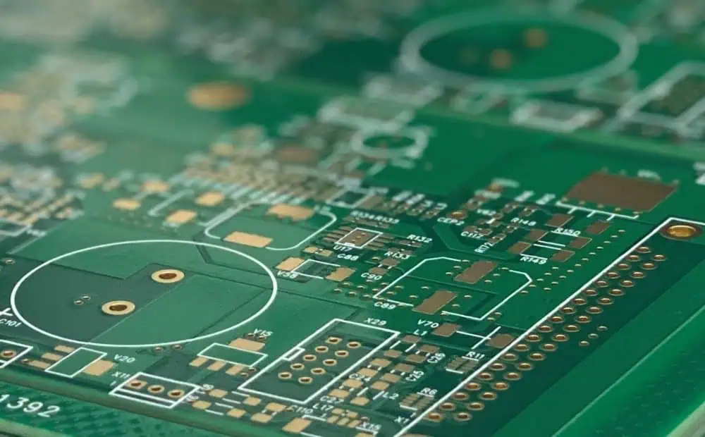
In the world of electronics manufacturing, efficiency and cost-effectiveness are paramount. One technique that has revolutionized the production of printed circuit boards (PCBs) is panelization. This article delves into the intricacies of PCB panelization, exploring its benefits, challenges, and best practices for optimal results.
What is PCB Panelization?
PCB panelization is the process of combining multiple individual PCB designs into a single, larger panel for more efficient manufacturing. This technique allows for the simultaneous production of multiple boards, significantly reducing manufacturing time and costs. Panelization is especially beneficial for high-volume production runs and smaller PCB designs.
By arranging multiple PCB layouts on a single panel, manufacturers can optimize material usage, streamline the production process, and enhance overall efficiency. This approach is particularly advantageous for mass production scenarios, where even small improvements in efficiency can lead to substantial cost savings.
The size of a PCB panel can vary depending on several factors, including:
Manufacturing equipment capabilities
Design requirements
Production volume
Material constraints
Typically, PCB panels range from 18″ x 24″ (457mm x 610mm) to 21″ x 24″ (533mm x 610mm). However, some manufacturers may offer custom panel sizes to accommodate specific project needs. It’s crucial to consult with your PCB manufacturer to determine the optimal panel size for your particular requirements.
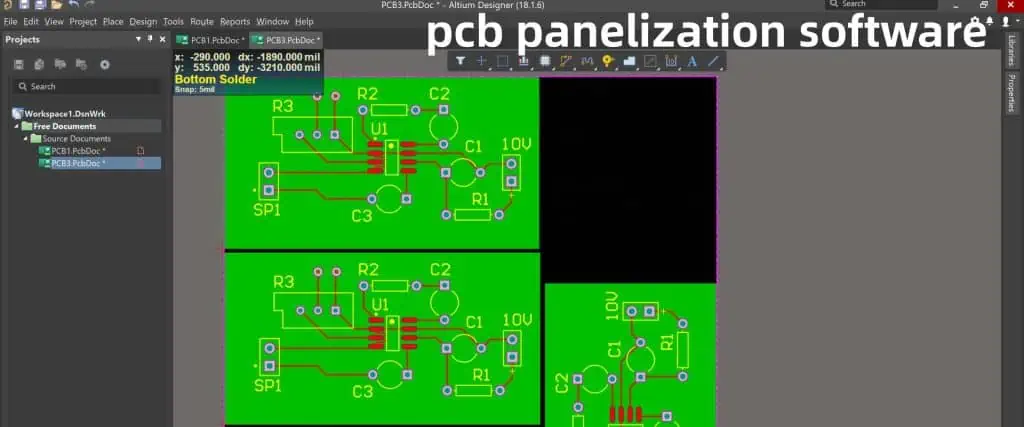
Tools for PCB Panelization
To effectively implement PCB panelization, designers and manufacturers rely on various specialized tools. These tools help in the planning, execution, and optimization of the panelization process:
CAD Software: Advanced PCB design software like Altium Designer, Eagle, and KiCad often include panelization features.
Panelization Software: Dedicated tools like PanelizeXT and Wise Panelize focus specifically on creating optimized panel layouts.
Gerber Editors: Software like GerbTool and CAM350 allow for manual adjustments and fine-tuning of panelized designs.
Simulation Tools: Programs that simulate the manufacturing process help identify potential issues before production begins.
Automated Panelization Systems: Some manufacturers use automated systems that optimize panel layouts based on input parameters.
What Types of PCB Panel Designs Are There?
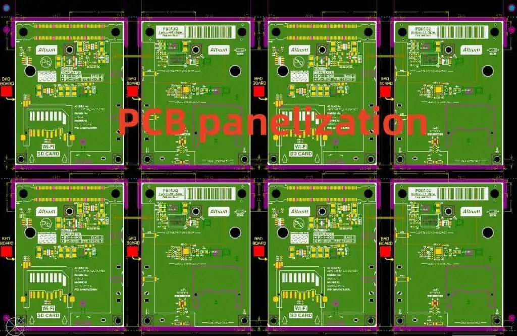
Figure 2,Panelization of two different PCB-designs
PCB panelization offers various design approaches, each suited to different manufacturing requirements and board characteristics. Let’s explore the main types:
1. Order Panelization
Order Panelization
Order panelization involves arranging identical PCB designs in a grid pattern on the panel. This method is ideal for high-volume production of a single PCB design, maximizing efficiency and minimizing waste.
2. Rotation Angle Panelization
Rotation Angle Panelization
In this approach, PCB designs are rotated at different angles within the panel. This technique can help optimize space utilization, especially for irregularly shaped PCBs. It also allows for more efficient use of panel area, potentially reducing material waste.
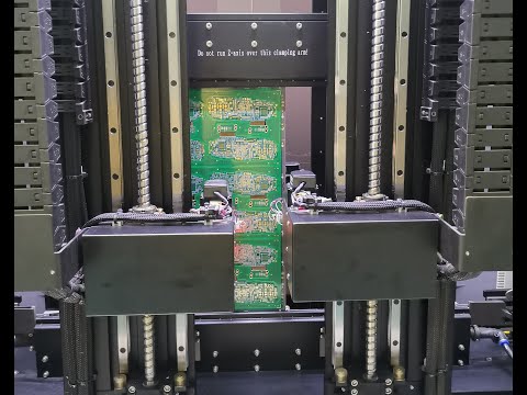
3. Double Side Panelization
Double side panelization
Double side panelization involves placing PCB designs on both sides of the panel. This method is particularly useful for double-sided or multi-layer PCBs, allowing for simultaneous production of both sides and potentially reducing manufacturing time.
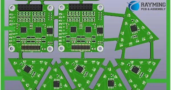
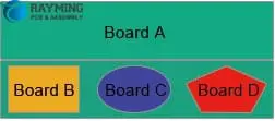
4. Combination Panelization
Combination Panelization
Combination panelization integrates different PCB designs onto a single panel. This approach is beneficial when producing multiple designs in smaller quantities, allowing for efficient use of panel space and reducing overall production costs.
5. Combination Panelization (ABCD)
ABCD panelization is a specific form of combination panelization where four different PCB designs (A, B, C, and D) are arranged on a single panel. This method is ideal for producing small quantities of multiple designs simultaneously, offering flexibility and cost-effectiveness for diverse production needs.
PCB Panelization – Factors to Consider
Effective PCB panelization requires careful consideration of various factors to ensure optimal results. Let’s examine these crucial aspects:
1. Challenges and Solutions in Panelization
Panelization can present challenges such as:
Ensuring uniform board quality across the panel
Managing thermal expansion during manufacturing
Maintaining consistent electrical properties
Solutions include:
Implementing proper spacing between boards
Using dummy circuits to balance copper distribution
Employing advanced simulation tools to predict and mitigate issues
2. Component Placement
Careful component placement is crucial in panelization. Consider:
Edge clearances for components
Orientation of sensitive components
Balancing component distribution across the panel
3. Trace Routing
Efficient trace routing in panelized designs involves:
Incorporating test points accessible in panelized form
Designing for compatibility with automated assembly equipment
Considering in-circuit and functional testing requirements
7. Cost
Balance cost considerations by:
Maximizing panel utilization
Optimizing for standard panel sizes
Considering material selection and layer count
11 Essential Design Rules for PCB Panelization
panel pcb
To ensure successful PCB panelization, adhere to these essential design rules:
Maintain consistent board orientation for efficient assembly.
Use breakaway tabs or V-scoring for easy depanelization.
Implement proper fiducial marks for accurate component placement.
Ensure adequate clearance between boards and panel edges.
Balance copper distribution across the panel to prevent warping.
Design tooling holes for proper panel alignment during manufacturing.
Consider the direction of manufacturing processes (e.g., etching, plating) in layout.
Implement proper test points accessible in panelized form.
Use panel borders to protect edge components during handling.
Optimize panel utilization to minimize waste.
Ensure compatibility with automated assembly and testing equipment.
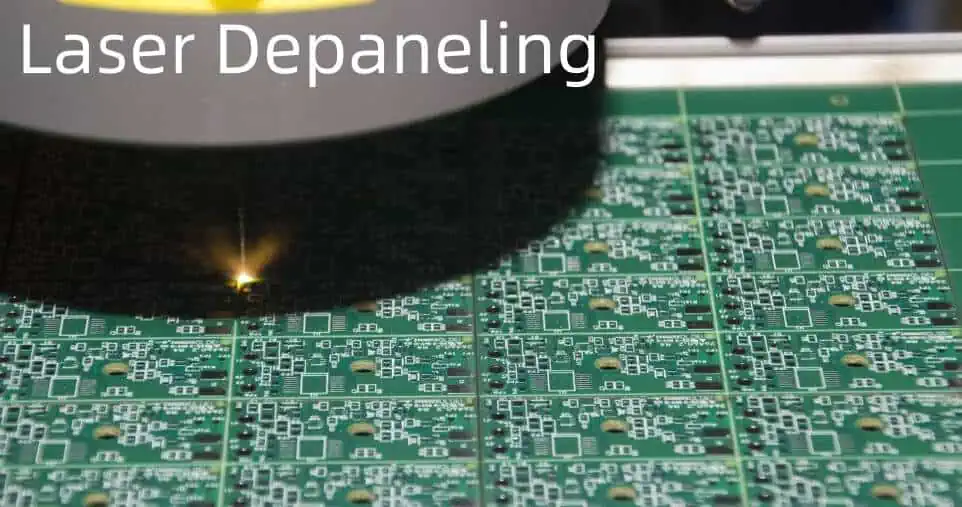
How to Depanelize?
Depanelization is the process of separating individual PCBs from the panel after manufacturing. The choice of depanelization method depends on factors such as board design, material properties, and production volume.
Depanelization Methods
Common depanelization techniques include:
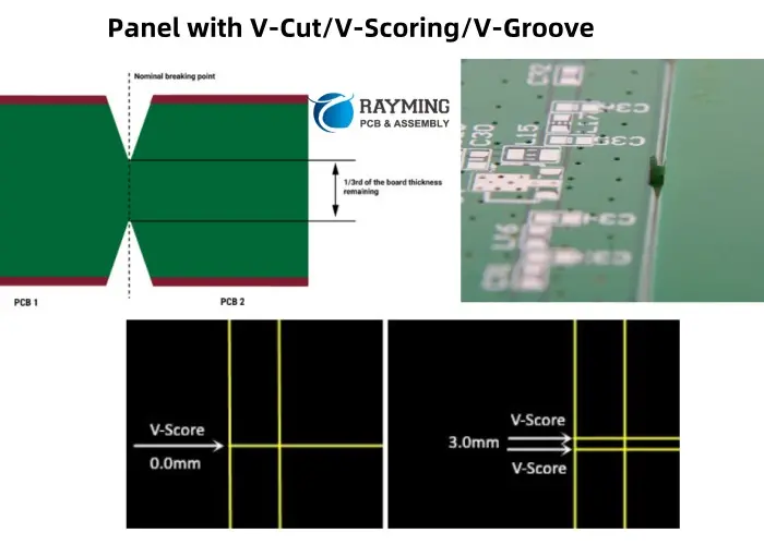
V-Scoring: Creating partially-cut grooves along separation lines.
Tab Routing: Using routed slots with small tabs to hold boards in place.
Perforation: Creating a series of small holes along separation lines.
Laser Cutting: Using precision laser technology for clean separation.
Water Jet Cutting: Employing high-pressure water for separation.
V-Scoring
V-scoring is a popular depanelization method that involves:
Creating V-shaped grooves on both sides of the panel
Allowing for easy manual separation or breakout
Providing clean edges with minimal stress on components
Tab Routing
Tab routing offers several advantages:
Allows for complex board shapes
Provides better support for larger or heavier boards
Enables easier separation of densely populated boards
What Factors Affect Panel Prices?
Several factors influence the cost of PCB panels:
1. Usable Area of Working Panel
The efficient utilization of panel space directly impacts cost. Maximizing the usable area reduces waste and lowers per-unit costs.
2. The Cost of Substrates and Films
Material selection significantly affects panel prices. Factors include:
Base material (e.g., FR-4, high-frequency materials)
Specialized testing for high-frequency or high-power designs
6. Expedited Fee
Rush orders or expedited production typically incur additional costs. Consider:
Standard vs. expedited turnaround times
Impact on manufacturing schedule
Balancing urgency with cost-effectiveness
Advantages of PCB Panelization
PCB panelization offers numerous benefits to manufacturers and designers alike:
1. Reduced Costs
Panelization significantly reduces production costs by:
Minimizing material waste
Lowering per-unit manufacturing costs
Optimizing equipment utilization
2. Improved Efficiency
Efficiency gains from panelization include:
Faster production times for multiple boards
Streamlined assembly and testing processes
Reduced handling and transportation requirements
3. Easier Assembly
Panelization facilitates easier assembly by:
Enabling batch processing of components
Improving compatibility with automated assembly equipment
Reducing the risk of damage to individual boards during handling
In conclusion, PCB panelization is a crucial technique in modern electronics manufacturing. By carefully considering design factors, adhering to best practices, and leveraging the advantages of panelization, designers and manufacturers can achieve significant cost savings and efficiency improvements. As the electronics industry continues to evolve, mastering the art of PCB panelization will remain a key factor in staying competitive and meeting the demands of increasingly complex designs.
Are you curious about how modern electronics are made? At the heart of many devices lies a crucial component: the printed circuit board (PCB). And at the core of PCB fabrication is an unsung hero – dry film photoresist. In this article, we’ll dive into the world of dry film photoresist and explore its vital role in creating the electronics we use every day.
The Fundamentals of Dry Film Photoresist
Defining Dry Film Photoresist
Dry film photoresist is a photosensitive material central to PCB production. It consists of a photopolymer layer sandwiched between two protective sheets. When exposed to ultraviolet (UV) light, the photoresist undergoes a chemical transformation, enabling precise pattern transfer onto the PCB substrate.
The Journey of Photoresist Technology
The evolution of photoresist technology in PCB manufacturing has been nothing short of remarkable. From the initial use of liquid photoresists to the development of dry film alternatives, this technology has continuously adapted to meet the escalating demands of the electronics industry.
The Liquid Photoresist Era
In the early days of PCB fabrication, liquid photoresists were the primary solution. While effective, they presented challenges in terms of uniformity and handling, particularly for high-volume production scenarios.
The Dry Film Photoresist Revolution
The introduction of dry film photoresist marked a turning point in PCB manufacturing. This innovation addressed many of the shortcomings of liquid photoresists, offering improved consistency, ease of use, and compatibility with automated processes.
Key Benefits of Dry Film Photoresist
Unparalleled Uniformity and Thickness Control
A primary advantage of dry film photoresist is its ability to provide exceptional uniformity across the PCB surface. This consistency is crucial for achieving precise circuit patterns, especially in high-density designs where every micron matters.
Superior Resolution and Edge Definition
Dry film photoresist enables sharper edge definition and higher resolution in circuit patterns. This capability is invaluable as PCBs become increasingly complex and compact, necessitating finer lines and spaces.
Streamlined Handling and Processing
The solid nature of dry film photoresist simplifies handling and application compared to liquid alternatives. It can be easily laminated onto PCB substrates, minimizing the risk of contamination and ensuring more comprehensive coverage.
Eco-friendly and Health-conscious
Dry film photoresist is generally considered more environmentally friendly than its liquid counterparts. It generates less waste and reduces exposure to potentially harmful chemicals during the application process, aligning with modern sustainability goals.
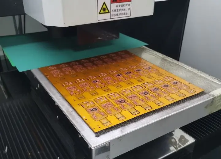
The Dry Film Photoresist Workflow in PCB Production
Dry File Imaging Process of Aluminum PCB Manufactturing
Phase 1: Surface Preparation and Cleaning
Before applying dry film photoresist, the PCB substrate undergoes thorough cleaning to ensure optimal adhesion. This crucial step typically involves mechanical or chemical cleaning processes to eliminate surface contaminants.
Phase 2: Lamination Process
The dry film photoresist is carefully laminated onto the PCB substrate using a combination of heat and pressure. This process ensures uniform coverage and strong adhesion to the board surface, setting the stage for subsequent steps.
Phase 3: UV Exposure
The laminated board is exposed to UV light through a photomask containing the desired circuit pattern. This exposure triggers polymerization in the exposed areas, creating a hardened image of the circuit design.
Phase 4: Development Stage
Following exposure, the board undergoes a development process. This step removes the unexposed photoresist, leaving behind the desired circuit pattern and preparing the board for etching.
Phase 5: Etching Process
With the protective photoresist pattern in place, the board is subjected to an etching process. This step removes the exposed copper, creating the final circuit pattern with precision.
Phase 6: Resist Stripping
Once etching is complete, the remaining photoresist is stripped away, revealing the finished circuit pattern on the PCB and concluding the core fabrication process.
Diverse Applications of Dry Film Photoresist in PCB Manufacturing
High-Density Interconnect (HDI) PCBs
Dry film photoresist plays a pivotal role in the production of HDI PCBs, which demand extremely fine lines and spaces. Its high resolution and excellent edge definition make it ideal for these cutting-edge applications.
Flexible PCB Solutions
The adaptability of dry film photoresist makes it well-suited for manufacturing flexible PCBs. These versatile boards are increasingly used in compact electronic devices and wearable technology, where flexibility is paramount.
Multilayer PCB Fabrication
In the production of multilayer PCBs, dry film photoresist is used to create precise patterns on each layer. Its consistency and reliability are essential for ensuring proper alignment and functionality across all layers of these complex boards.
Rigid-Flex PCB Integration
Rigid-flex PCBs, which combine rigid and flexible board technologies, benefit significantly from the versatility of dry film photoresist. It can be effectively applied to both rigid and flexible substrates, ensuring uniform circuit patterns throughout the hybrid board.
Navigating Challenges in Dry Film Photoresist Usage
Optimal Storage and Handling Practices
Dry film photoresist is sensitive to environmental factors such as light, temperature, and humidity. Implementing proper storage and handling procedures is crucial to maintain its quality and effectiveness throughout its shelf life.
Precision in Equipment and Process Control
Achieving optimal results with dry film photoresist requires precise control over various process parameters, including lamination temperature, exposure time, and development conditions. This level of control demands sophisticated equipment and well-trained operators.
Ensuring Substrate Compatibility
While dry film photoresist is versatile, ensuring compatibility with various PCB substrate materials can be challenging. Different substrates may require specific types of photoresist or modified processing conditions to achieve optimal results.
Application-Specific Optimization
Each PCB application may have unique requirements in terms of resolution, thickness, and other properties. Fine-tuning the dry film photoresist process to meet these specific needs can be complex and time-consuming, requiring expertise and patience.
Innovation Horizons in Dry Film Photoresist Technology
Next-Generation Photoresist Formulations
Ongoing research is focused on developing new photoresist formulations with improved properties, such as higher resolution, better adhesion, and enhanced resistance to harsh manufacturing conditions, pushing the boundaries of what’s possible in PCB fabrication.
Synergy with Additive Manufacturing
As additive manufacturing techniques gain traction in PCB production, dry film photoresist technology is evolving to support these new processes, offering potential for even more precise and efficient circuit creation in the era of 3D-printed electronics.
Eco-Innovation in Photoresist Solutions
The push for more sustainable manufacturing practices is driving the development of eco-friendly dry film photoresist options, with a focus on reducing environmental impact, improving recyclability, and minimizing the carbonfootprint of PCB production.
Industry 4.0 Integration
The integration of dry film photoresist processes with advanced automation and Industry 4.0 technologies promises to enhance efficiency, reduce errors, and improve overall PCB manufacturing quality, ushering in a new era of smart manufacturing in the electronics industry.
Conclusion: The Enduring Significance of Dry Film Photoresist
As we’ve explored throughout this article, dry film photoresist stands as a cornerstone technology in the realm of PCB fabrication. Its capacity to deliver precision, consistency, and versatility makes it an indispensable tool in the electronics manufacturing industry.
From enabling the production of high-density interconnect boards to supporting the development of flexible and multilayer PCBs, dry film photoresist continues to push the envelope of possibility in circuit board design and manufacturing. Its ongoing evolution, driven by relentless research and innovation, ensures that it will remain at the forefront of PCB manufacturing technology for years to come.
As electronic devices become increasingly compact, complex, and ubiquitous, the role of dry film photoresist in PCB fabrication is set to grow even more critical. It stands as a testament to the ingenuity and continuous improvement that drives the electronics industry forward, playing a vital role in shaping the electronic landscape of tomorrow.
For PCB designers, manufacturers, and technology enthusiasts alike, understanding the role of dry film photoresist provides valuable insight into the precision and innovation that underpins our modern digital world. As we look to the future, it’s clear that this unassuming yet critical technology will continue to be a key player in the ongoing revolution of electronic design and manufacturing.
Monopole antennas have been a cornerstone of wireless communication technology for decades. These simple yet versatile antennas are found in a wide range of applications, from radio broadcasting to modern mobile devices. In this comprehensive guide, we’ll explore the intricacies of monopole antenna design, delving into various types and their applications, with a particular focus on quarter-wave, planar, and ultra-wideband (UWB) configurations.
Understanding Monopole Antennas
What is a Monopole Antenna?
A monopole antenna is a type of radio antenna consisting of a straight rod-shaped conductor, often mounted perpendicularly to a ground plane. It is essentially one half of a dipole antenna, with the ground plane serving as a mirror for the missing half. This design makes monopole antennas compact and easy to integrate into various devices.
Basic Principles of Operation
Monopole antennas operate by converting electrical signals into electromagnetic waves and vice versa. The conductor element oscillates with the applied alternating current, creating an electromagnetic field that radiates outward. The ground plane plays a crucial role in shaping the radiation pattern and improving the antenna’s efficiency.
Advantages of Monopole Antennas
Simplicity: Monopole antennas are straightforward in design and easy to construct.
Compact size: They require less space compared to full dipole antennas.
Omnidirectional radiation pattern: Ideal for applications requiring 360-degree coverage.
Cost-effective: Simple design translates to lower manufacturing costs.
Versatility: Suitable for a wide range of frequencies and applications.
Quarter-Wave Monopole Antenna Design
Principles of Quarter-Wave Antennas
The quarter-wave monopole is one of the most common and efficient monopole antenna designs. As the name suggests, its length is approximately one-quarter of the wavelength of the operating frequency. This design creates a standing wave pattern that results in efficient radiation.
Calculating Antenna Length
To calculate the length of a quarter-wave monopole antenna, use the following formula:
L = (c / f) * 0.25
Where:
L is the length of the antenna
c is the speed of light (approximately 3 x 10^8 m/s)
f is the frequency of operation
Impedance Matching
Quarter-wave monopoles typically have an impedance of around 36.5 ohms when used with a perfect ground plane. To match this to standard 50-ohm systems, techniques such as:
Using a matching network
Adjusting the antenna’s thickness
Employing a folded monopole design
can be implemented to achieve optimal performance.
Ground Plane Considerations
The size and shape of the ground plane significantly affect the antenna’s performance. A larger ground plane generally improves efficiency and radiation pattern symmetry. In practice, a ground plane with a radius of at least one-quarter wavelength is often recommended.
Planar monopole antennas are a modern variation of the traditional monopole design. They consist of a flat, often rectangular or circular, conductive element mounted perpendicular to a ground plane. These antennas offer several advantages, including:
Low profile
Easy integration into printed circuit boards (PCBs)
Potential for wide bandwidth operation
Design Considerations
When designing planar monopole antennas, several factors need to be considered:
Shape of the planar element
Feed point location
Ground plane size and shape
Substrate material and thickness (for PCB-integrated designs)
Common Shapes and Their Characteristics
Rectangular Planar Monopole:
Simple to design and fabricate
Bandwidth can be enhanced by beveling or smoothing corners
Circular Planar Monopole:
Offers wider bandwidth compared to rectangular designs
More uniform radiation pattern
Elliptical Planar Monopole:
Provides a good compromise between rectangular and circular designs
Allows for some control over bandwidth and radiation characteristics
Feeding Techniques
Several feeding techniques can be employed for planar monopole antennas:
Ultra-wideband technology operates across a wide range of frequencies, typically from 3.1 GHz to 10.6 GHz. UWB systems require antennas capable of maintaining consistent performance across this broad spectrum.
Challenges in UWB Antenna Design
Designing UWB monopole antennas presents several challenges:
Maintaining consistent impedance matching across the entire bandwidth
Achieving stable radiation patterns over the frequency range
Miniaturization while preserving performance
Managing group delay variations
UWB Monopole Antenna Configurations
Several monopole configurations have been developed to meet UWB requirements:
Effective for antenna array design and pattern synthesis
Neural Networks:
Machine learning approach to antenna design
Can predict performance and assist in rapid prototyping
Measurement and Characterization
Accurate measurement and characterization are crucial for validating monopole antenna designs:
Vector Network Analyzer (VNA):
Measures S-parameters for impedance matching and bandwidth analysis
Anechoic Chamber:
Provides a controlled environment for radiation pattern measurements
Near-field Scanning:
Allows for high-resolution characterization of antenna performance
Future Trends in Monopole Antenna Design
Miniaturization and Integration
As devices continue to shrink, monopole antenna designs are evolving to meet size constraints:
Chip Antennas:
Extremely compact designs for integration into small IoT devices
3D-Printed Antennas:
Allows for complex geometries and customization
Textile-Integrated Antennas:
Flexible monopole designs for wearable technology
Multi-band and Reconfigurable Antennas
Future monopole designs are focusing on adaptability:
Frequency-Reconfigurable Monopoles:
Antennas that can switch between different frequency bands
Pattern-Reconfigurable Antennas:
Ability to adjust radiation patterns for optimal performance
Cognitive Radio Antennas:
Monopoles capable of adapting to dynamic spectrum usage
Advanced Materials
Emerging materials are opening new possibilities for monopole antenna design:
Graphene-based Antennas:
Extremely thin and flexible designs with unique properties
Liquid Metal Antennas:
Reconfigurable antennas using fluid conductors
Metamaterial-Inspired Designs:
Engineered structures for enhanced performance and miniaturization
Conclusion
Monopole antennas have come a long way from their simple quarter-wave origins. Today, they encompass a wide range of designs, from planar structures to ultra-wideband configurations. As we’ve explored in this comprehensive guide, monopole antennas continue to play a crucial role in modern wireless communication systems, IoT devices, and emerging technologies.
The versatility and simplicity of monopole antennas ensure their relevance in an ever-evolving technological landscape. From the basic principles of quarter-wave designs to the cutting-edge developments in UWB and reconfigurable antennas, the field of monopole antenna design remains dynamic and full of innovation.
As we look to the future, monopole antennas will undoubtedly continue to adapt and evolve, meeting the challenges of miniaturization, integration, and multi-functionality. Whether it’s in the next generation of mobile devices, advanced IoT ecosystems, or yet-to-be-imagined applications, monopole antennas will remain at the forefront of wireless technology, connecting our world in increasingly sophisticated ways.
In the ever-evolving landscape of wireless communication, antennas play a pivotal role in enabling seamless connectivity across a myriad of devices. From smartphones and laptops to IoT sensors and wearable technology, the demand for compact, efficient, and versatile antennas has never been greater. Enter the Inverted-F Antenna (IFA) and its planar cousin, the Planar Inverted-F Antenna (PIFA) – two designs that have revolutionized the world of compact wireless devices.
The Inverted-F Antenna, aptly named for its “F” shaped profile, has become a cornerstone in modern wireless design. Its low-profile structure, ease of integration, and impressive performance characteristics make it an ideal choice for engineers and designers working on space-constrained devices. The PIFA, an evolution of the IFA, takes these advantages further by offering even greater flexibility in terms of size and bandwidth potential.
As we dive into the world of Inverted-F Antenna designs, we’ll explore their fundamental principles, design strategies, and practical applications. This comprehensive guide is crafted to equip you with the knowledge and tools necessary to harness the full potential of IFA and PIFA designs in your projects. Whether you’re working on a 2.4 GHz Wi-Fi device, a dual-band mobile phone antenna, or an embedded IoT solution, this article will serve as your roadmap to success.
The Inverted-F Antenna (IFA) is a type of internal antenna commonly used in wireless communication devices. It derives its name from its shape, which resembles an inverted letter “F” when viewed from the side. The IFA evolved from the Inverted-L Antenna (ILA) design, with the addition of a short-circuit stub to improve impedance matching and bandwidth.
Originating in the early days of mobile phone technology, the IFA quickly gained popularity due to its compact size and ability to be easily integrated into handheld devices. As wireless technology progressed, so did the IFA design, leading to variations like the Planar Inverted-F Antenna (PIFA).
Basic Structure and Working Principle
The basic structure of an Inverted-F Antenna consists of three main parts:
Radiating element: A horizontal arm that is typically a quarter-wavelength long at the operating frequency.
Short-circuit stub: A vertical element connecting one end of the radiating element to the ground plane.
Feed point: The point where the antenna is excited, usually located between the short-circuit stub and the open end of the radiating element.
The working principle of the IFA is based on the quarter-wave resonator concept. The short-circuit stub creates a virtual ground point, allowing the horizontal arm to act as a quarter-wavelength resonator. This configuration enables the antenna to resonate at a lower frequency than its physical size would typically allow, making it ideal for compact devices.
Differences Between IFA and PIFA
While the IFA and PIFA share many similarities, there are key differences:
Structure:
IFA: Uses a wire or narrow strip for the radiating element.
PIFA: Employs a planar element, often a rectangular patch.
Bandwidth:
IFA: Generally has a narrower bandwidth.
PIFA: Offers wider bandwidth potential due to its planar structure.
Size:
IFA: Can be made very compact but may protrude from the device.
PIFA: Typically flatter and more easily integrated into slim devices.
Radiation pattern:
IFA: Often more directional.
PIFA: Generally provides more omnidirectional coverage.
Key Advantages: Low Profile, Ease of Integration, Wide Bandwidth Potential
Inverted-F Antennas, particularly PIFAs, offer several advantages that make them popular in modern wireless devices:
Low profile: The compact design allows for easy integration into slim devices without significant protrusion.
Ease of integration: IFAs and PIFAs can be directly etched onto PCBs or implemented as surface-mount components.
Wide bandwidth potential: Especially with PIFAs, achieving multi-band or wideband operation is possible through various design techniques.
Good performance: Despite their small size, these antennas can provide efficient radiation and good gain characteristics.
Versatility: The design can be easily modified to suit different frequency bands and applications.
Cost-effective: IFAs and PIFAs can be manufactured using standard PCB processes, making them economical for mass production.
These advantages have made Inverted-F Antennas the go-to choice for many mobile, IoT, and compact wireless applications, driving innovation in antenna design and integration techniques.
2. Fundamental Concepts Behind Inverted-F Antenna Design
Understanding the core principles that govern Inverted-F Antenna behavior is crucial for effective design. Let’s delve into the key concepts that form the foundation of IFA and PIFA design.
Resonance Principles and Quarter-Wavelength Operation
The Inverted-F Antenna operates on the principle of quarter-wavelength resonance. Here’s how it works:
Quarter-wave resonator: The main radiating element is approximately a quarter-wavelength long at the desired operating frequency.
Virtual ground: The short-circuit stub creates a virtual ground point, allowing the antenna to resonate at a lower frequency than its physical length would suggest.
Resonance frequency: The fundamental resonance frequency (f) is approximately given by:f = c / (4 * L)Where c is the speed of light, and L is the effective length of the radiating element.
Higher-order modes: IFAs and PIFAs can also operate at odd multiples of the fundamental frequency, enabling multi-band operation.
Impedance Matching and Tuning Methods
Proper impedance matching is critical for efficient power transfer between the antenna and the transceiver. Key aspects include:
Feed point location: The position of the feed point along the radiating element significantly affects the input impedance. Moving it closer to the short-circuit stub lowers the impedance.
Short-circuit stub width: Adjusting the width of the short-circuit stub can fine-tune the impedance.
Matching networks: External components like capacitors and inductors can be used to achieve better impedance matching across a wider bandwidth.
Slotting and meandering: Introducing slots or meandering in the radiating element can alter its electrical length and impedance characteristics.
Importance of Ground Plane Design
The ground plane plays a crucial role in the performance of Inverted-F Antennas:
Size effects: A larger ground plane generally improves antenna efficiency and bandwidth but may not always be practical in compact devices.
Edge effects: The edges of the ground plane contribute significantly to radiation. Optimizing the antenna’s position relative to the ground plane edges can enhance performance.
Current distribution: The ground plane carries induced currents that contribute to the overall radiation pattern. Understanding and managing these currents is key to optimizing antenna performance.
Clearance area: Maintaining a clear area around the antenna on the ground plane is essential for proper operation.
Radiation Patterns Typical for IFA and PIFA
The radiation patterns of Inverted-F Antennas are influenced by their structure and the ground plane:
IFA radiation pattern:
Generally more directional
Maximum radiation often perpendicular to the ground plane
Pattern can be shaped by adjusting the antenna’s position relative to the ground plane edges
PIFA radiation pattern:
More omnidirectional compared to IFA
Tends to provide better coverage in multiple directions
Can be optimized for specific applications by modifying the patch shape and feed position
Understanding these fundamental concepts provides the foundation for effective Inverted-F Antenna design. In the following sections, we’ll explore how to apply these principles to create antennas for specific applications and frequencies.
3. Designing an Inverted-F Antenna for 2.4 GHz Applications
The 2.4 GHz band is a cornerstone of modern wireless communication, hosting popular protocols like Wi-Fi, Bluetooth, and Zigbee. Designing an Inverted-F Antenna for this frequency requires careful consideration of various factors. Let’s walk through the process step-by-step.
Key 2.4 GHz Applications
Before diving into the design process, it’s important to understand the primary applications for 2.4 GHz antennas:
Wi-Fi (IEEE 802.11b/g/n): Requires good bandwidth coverage from 2.4 GHz to 2.4835 GHz.
Bluetooth: Operates in the 2.4 GHz to 2.4835 GHz range.
Zigbee: Uses channels within the 2.4 GHz to 2.4835 GHz band.
IoT devices: Many IoT protocols operate in this band due to its global availability.
Step-by-Step Design Guide
1. Determining Dimensions Based on the Target Frequency
To design an IFA for 2.4 GHz:
a) Calculate the quarter-wavelength at 2.4 GHz: λ/4 = c / (4 * f) = (3 * 10^8) / (4 * 2.4 * 10^9) ≈ 31.25 mm
b) Adjust for the effective dielectric constant of your PCB material. For FR-4 (εr ≈ 4.4), the length will be approximately: L ≈ 31.25 mm / √εr ≈ 14.9 mm
c) The width of the radiating element typically ranges from 1-3 mm for PCB implementations.
d) The height of the short-circuit stub affects bandwidth and can be optimized, but typically starts at about 3-5 mm.
2. Material and PCB Substrate Choices
Common materials for 2.4 GHz IFAs include:
FR-4: Cost-effective and widely available, suitable for many applications.
RogersRO4350B: Offers better performance but at a higher cost.
Taconic RF-35: Another high-performance option for demanding applications.
Consider factors like dielectric constant, loss tangent, and thermal stability when choosing your substrate.
3. Optimizing Feed Point Location for Impedance Matching
The feed point location is crucial for achieving good impedance matching:
a) Start with the feed point at about 30% of the total length from the short-circuit stub. b) Use simulation tools or a vector network analyzer to fine-tune the position for best VSWR or return loss at 2.4 GHz. c) Aim for an input impedance close to 50 ohms to match common RF systems.
4. Ground Plane Considerations
For optimal performance at 2.4 GHz:
a) Aim for a ground plane at least λ/4 in length and width (about 31.25 mm at 2.4 GHz). b) Keep a clearance area of at least 5-10 mm around the antenna on the ground plane. c) Consider the effects of nearby components and device housing on the effective ground plane size.
Common Pitfalls When Designing for 2.4 GHz
Ignoring environmental factors: The presence of a plastic case or nearby components can detune the antenna.
Insufficient bandwidth: Ensure your design covers the entire 2.4 GHz to 2.4835 GHz range for protocols like Wi-Fi and Bluetooth.
Poor impedance matching: Neglecting proper feed point optimization can result in high VSWR and poor efficiency.
Overlooking manufacturing tolerances: Small variations in PCB etching can significantly affect performance at 2.4 GHz.
Inadequate ground plane: A too-small ground plane can severely impact antenna performance.
By following this guide and being aware of common issues, you can design an effective Inverted-F Antenna for 2.4 GHz applications. Remember that simulation and real-world testing are crucial steps in the design process, which we’ll cover in later sections.
4. Dual-Band Inverted-F Antenna Design Strategies
As wireless devices increasingly support multiple frequency bands, the ability to design dual-band antennas becomes crucial. Inverted-F Antennas, particularly PIFAs, are well-suited for multi-band operation with proper design techniques. Let’s explore strategies for creating effective dual-band IFA and PIFA designs.
Why Dual-Band is Important
Dual-band antennas offer several advantages:
Multi-protocol support: e.g., Wi-Fi 2.4 GHz and 5 GHz in a single antenna.
Cellular coverage: Supporting multiple LTE bands with one antenna.
Space efficiency: Combining multiple frequency bands in a single antenna saves valuable space in compact devices.
Cost-effectiveness: One dual-band antenna can replace two single-band antennas, potentially reducing production costs.
Techniques for Achieving Dual-Band Performance
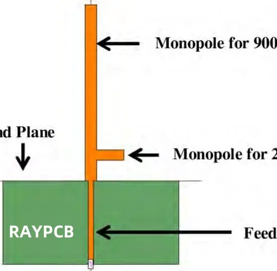
1. Multiple Feed Points
Concept: Use two separate feed points, each optimized for a different frequency band.
Implementation: a) Design two radiating elements of different lengths on the same structure. b) Feed each element separately, often requiring a diplexer or switch.
Advantages: Good isolation between bands, easier to tune independently.
Challenges: More complex feeding network, potentially larger size.
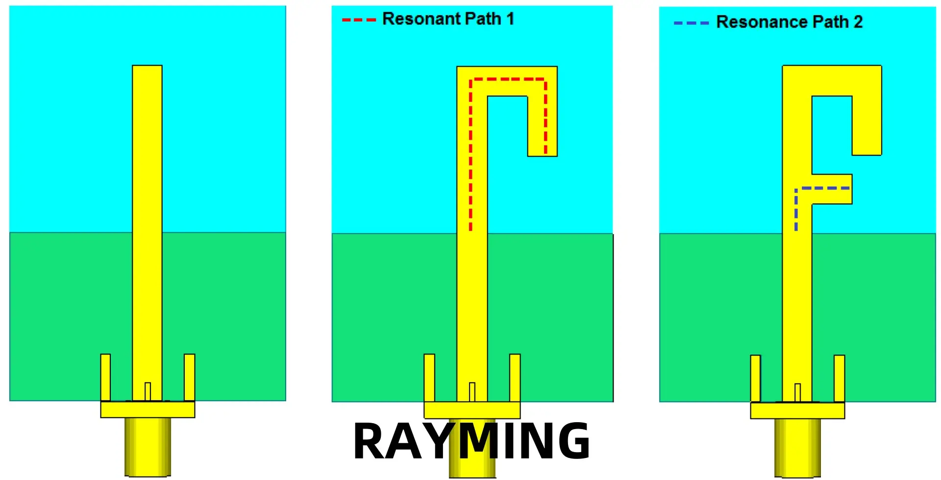
2. Slotted Designs
Concept: Introduce slots in the radiating element to create additional resonant paths.
Implementation: a) Add a U-shaped or L-shaped slot to a PIFA patch. b) Carefully tune the slot dimensions to achieve resonance at the desired higher frequency.
Advantages: Compact design, single feed point.
Challenges: Bandwidth at each frequency may be limited, careful tuning required.
3. Adding Parasitic Elements
Concept: Use a parasitic element to introduce a second resonance.
Implementation: a) Design the main radiating element for the lower frequency. b) Add a parasitic element near the main element, sized for the higher frequency. c) Adjust coupling between elements to fine-tune performance.
Advantages: Can achieve good bandwidth at both frequencies.
Challenges: Requires more space, coupling effects can be complex to manage.
4. Meandering and Branching Techniques
Concept: Create multiple resonant paths within a single structure.
Implementation: a) Design a meandering path for the lower frequency. b) Add branches or extensions tuned to the higher frequency.
Advantages: Compact design, single feed point.
Challenges: Can be sensitive to manufacturing tolerances.
Practical Examples of Dual-Band PIFA Structures
Wi-Fi Dual-Band PIFA (2.4 GHz and 5 GHz)
Main patch resonating at 2.4 GHz
U-shaped slot tuned for 5 GHz band
Single feed point for both bands
LTE Dual-Band PIFA (800 MHz and 1800 MHz)
Meandering main element for 800 MHz
Parasitic element or branch for 1800 MHz
Careful optimization of ground plane size for low-band efficiency
IoT Dual-Band PIFA (915 MHz and 2.4 GHz)
Main radiating element designed for 915 MHz (ISM band)
Slotted design or parasitic element for 2.4 GHz (Wi-Fi/Bluetooth)
Compact design suitable for small IoT devices
When designing dual-band Inverted-F Antennas, it’s crucial to consider the interaction between the two frequency bands. Simulation tools are invaluable for optimizing these complex structures and ensuring good performance across both bands.
5. Inverted-F Antennas in Mobile and Embedded Applications
The compact nature and versatile performance of Inverted-F Antennas make them ideal for mobile phones, IoT devices, and wearable technology. Let’s explore why these antennas are so well-suited for these applications and the unique design considerations they entail.
Why Inverted-F Antennas are Ideal for Mobile Phones, IoT, and Wearable Devices
Low profile: IFAs and PIFAs can be made very thin, fitting easily into slim smartphones and wearables.
Multiband operation: Capable of covering multiple frequency bands required for modern mobile communications.
Good performance in proximity to human body: PIFAs tend to be less affected by the presence of the user’s hand or head compared to some other antenna types.
Flexibility in design: Can be shaped to conform to device contours, especially important for wearables.
PCB integration: Can be directly etched onto the main PCB, saving space and reducing cost.
Examples of Smartphone Antenna Integration
Modern smartphones often use multiple Inverted-F Antennas to cover various bands and improve performance:
Main cellular antenna: Typically a PIFA design covering multiple LTE bands.
Diversity/MIMO antenna: Secondary PIFA for improved reception and data rates.
Wi-Fi/Bluetooth antenna: Often a separate IFA or PIFA optimized for 2.4 GHz and 5 GHz.
GPS antenna: A specialized PIFA design for GNSS frequencies.
Smartphone manufacturers often use clever techniques to hide antennas, such as:
Integrating antennas into the metal frame of the device
Using the back cover as part of the antenna structure
Implementing transparent antennas in the display area
Design Considerations for Embedded Antennas
Space Constraints
Miniaturization techniques: Use of meandering, folding, and 3D structures to reduce antenna size.
Co-design with device housing: Utilizing device chassis as part of the antenna system.
Ground plane optimization: Careful design of ground plane shape and size to maximize performance in limited space.
Nearby Component Effects
Detuning: Proximity of components can shift the antenna’s resonant frequency.
Isolation: Ensuring sufficient separation or shielding from noise sources like processors.
Coupling: Managing intentional and unintentional coupling with other antennas or components.
Human Body Interaction (Wearable Devices)
Body effect modeling: Simulating antenna performance when worn on different body parts.
SAR (Specific Absorption Rate) considerations: Designing to minimize RF energy absorption by the body.
Impedance stability: Ensuring the antenna remains well-matched when in contact with the body.
6. Simulation and Testing of Inverted-F Antennas
Proper simulation and testing are crucial for developing effective Inverted-F Antennas. This process helps optimize designs before physical prototyping and ensures that manufactured antennas meet performance specifications.
Introduction to Antenna Simulation Tools
Popular electromagnetic simulation software for antenna design includes:
Industry-standard for 3D electromagnetic field simulation
Excellent for complex antenna structures and environments
CST Microwave Studio:
Versatile tool with multiple solver technologies
Good for time-domain and frequency-domain analysis
FEKO (FEldberechnung für Körper mit beliebiger Oberfläche):
Specializes in Method of Moments (MoM) and hybrid techniques
Efficient for large structure simulations like antennas on vehicles
COMSOL Multiphysics:
Allows coupling of electromagnetic simulations with other physics (thermal, mechanical)
Useful for multiphysics problems in antenna design
Common Simulation Parameters to Analyze
When simulating Inverted-F Antennas, key parameters to focus on include:
S11 (Return Loss):
Indicates how well the antenna is matched to the feed line
Aim for S11 < -10 dB in the frequency band of interest
VSWR (Voltage Standing Wave Ratio):
Another measure of impedance matching
Target VSWR < 2:1 for good performance
Gain and Efficiency:
Analyze 3D radiation patterns and peak gain
Look at antenna efficiency across the operating band
Current Distribution:
Helps understand how the antenna is radiating
Useful for identifying potential improvements in the design
Near-field Distribution:
Important for assessing SAR and interaction with nearby components
Real-World Testing Methods
While simulation is valuable, real-world testing is essential to validate antenna performance:
Anechoic Chamber Measurements
Purpose: Provides a controlled environment for accurate antenna measurements
Measurements:
Far-field radiation patterns
Gain measurements
Efficiency testing
Return Loss and Impedance Testing
Equipment: Vector Network Analyzer (VNA)
Measurements:
S11 parameters
Input impedance across frequency
Bandwidth verification
Radiation Pattern Verification
Methods:
Far-field range testing
Near-field to far-field transformation techniques
Importance: Verifies the antenna’s directional characteristics and gain
Over-the-Air (OTA) Performance Testing
Purpose: Evaluates antenna performance in realistic usage scenarios
Measurements:
Total Radiated Power (TRP)
Total Isotropic Sensitivity (TIS)
Specific Absorption Rate (SAR) for body-worn devices
7. Common Challenges in Inverted-F Antenna Designs
Despite their many advantages, Inverted-F Antennas come with their own set of challenges. Understanding these issues is crucial for successful implementation.
Narrow Bandwidth Limitations
Issue: Basic IFA designs often have limited bandwidth, which can be problematic for wideband applications.
Solutions:
Use of broadbanding techniques like capacitive loading
Implementing slotted PIFA designs for increased bandwidth
Careful optimization of feed point and short-circuit stub placement
Tuning Issues During PCB Integration
Challenge: Antenna performance can change significantly when integrated into a complete PCB design.
Approaches:
Simulating the antenna with surrounding PCB components
Designing with tuning elements (e.g., capacitors) for post-integration adjustment
Maintaining proper clearance around the antenna area
Interference from Nearby Components
Problem: Proximity to other electronic components can detune the antenna or create unwanted coupling.
Mitigation strategies:
Proper placement and orientation of the antenna on the PCB
Use of ground planes or shielding to isolate the antenna
Careful routing of high-speed digital signals away from the antenna
De-tuning Caused by Environmental Changes
Issue: Factors like the user’s hand, device casing, or nearby objects can shift the antenna’s resonant frequency.
Solutions:
Designing for a slightly wider bandwidth to accommodate detuning
Implementing adaptive matching networks for dynamic tuning
Careful placement of the antenna within the device to minimize human body effects
8. Optimization Tips for High-Performance Inverted-F Antennas
To achieve the best possible performance from Inverted-F Antennas, consider these advanced optimization techniques:
Techniques for Maximizing Bandwidth
Parasitic elements: Adding nearby parasitic patches or strips can create additional resonances, widening the overall bandwidth.
Slotted designs: Carefully placed slots in PIFA structures can significantly increase bandwidth.
Thick substrates: Using a thicker PCB substrate can improve bandwidth, especially for PIFAs.
Tapered matching: Implementing a tapered feed section can provide better wideband matching.
Ground Plane Size and Shape Optimization
Edge tapering: Tapering the edges of the ground plane can smooth out resonances and improve bandwidth.
Slot cutting: Strategic slots in the ground plane can enhance radiation characteristics.
Size considerations: Optimizing the ground plane size relative to the operating wavelength can significantly impact performance.
Advanced Tuning Methods
Capacitive loading: Adding capacitance at the open end of the IFA can lower its resonant frequency without increasing size.
Inductive shorting: Replacing the shorting pin with an inductor can provide additional tuning flexibility.
Distributed matching networks: Implementing matching elements along the length of the antenna for improved wideband performance.
Balancing Size, Efficiency, and Frequency Stability
Miniaturization techniques: Use of meandering and 3D structures to reduce size while maintaining performance.
Material selection: Choosing high-quality, low-loss materials to maintain efficiency in compact designs.
Robust design practices: Implementing designs that are less sensitive to manufacturing tolerances and environmental changes.
9. Real-World Case Studies
Case Study 1: Designing a 2.4 GHz IFA for a Smart Sensor
Challenge: Create a compact, efficient antenna for a battery-powered IoT sensor operating at 2.4 GHz.
Solution:
Implemented a meandered IFA design to reduce overall size.
Optimized ground plane size to balance performance and compactness.
Used simulation to fine-tune feed point for best matching at 2.4 GHz.
Results:
Achieved -15 dB return loss across the entire 2.4 GHz ISM band.
Antenna efficiency of 75% in free space.
Successful integration into a compact 30mm x 30mm PCB.
Case Study 2: Dual-band PIFA for a Mobile Phone Application
Challenge: Design a single antenna to cover LTE Band 5 (850 MHz) and Band 3 (1800 MHz) for a slim smartphone.
Solution:
Implemented a slotted PIFA design with main resonance at 850 MHz.
Added a carefully tuned slot to create a second resonance at 1800 MHz.
Utilized the phone’s metal frame as part of the ground plane.
Results:
Achieved -10 dB bandwidth covering both required LTE bands.
Maintained performance with minimal detuning from hand effect.
Successfully integrated into a 7mm thick smartphone design.
Conclusion
Inverted-F Antennas, including their planar variants (PIFAs), represent a versatile and powerful solution for modern wireless communication challenges. Their ability to provide efficient, compact, and adaptable designs makes them indispensable in a world increasingly dominated by mobile and IoT devices.
Throughout this guide, we’ve explored the fundamental principles behind IFA and PIFA designs, delved into practical design strategies for single and dual-band applications, and addressed the unique challenges posed by mobile and embedded implementations. We’ve also covered essential aspects of simulation, testing, and optimization to ensure your antenna designs meet the demanding requirements of today’s wireless devices.
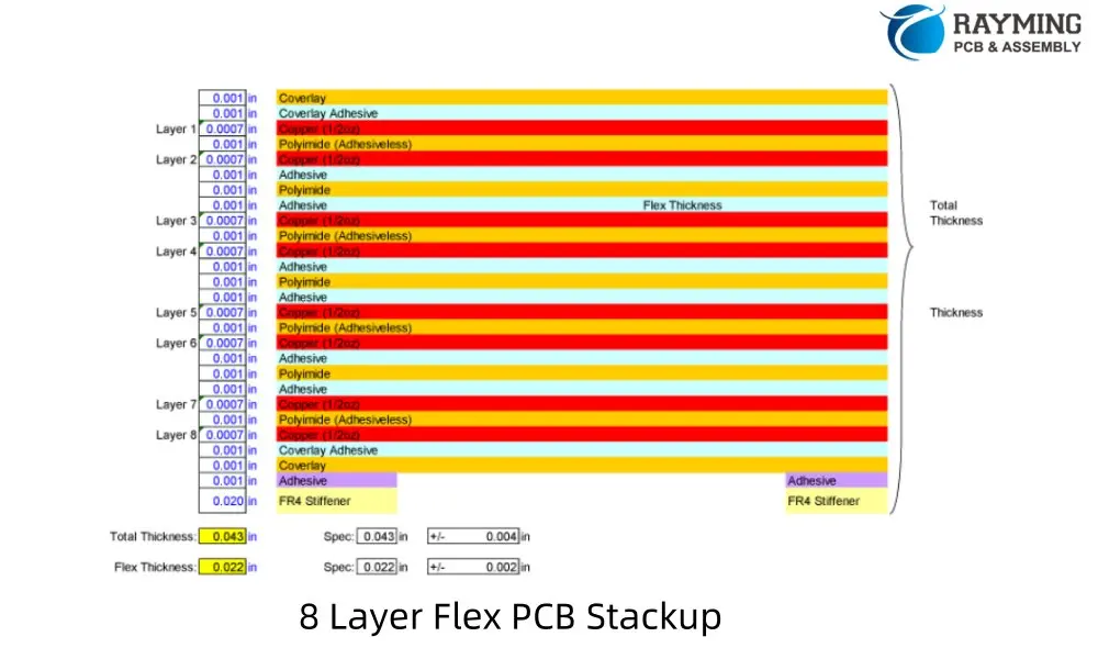
In the rapidly evolving world of electronics, the demand for more complex and compact circuitry continues to grow. Enter the 8 layer flexible PCB, a sophisticated solution that combines the benefits of multi-layer design with the versatility of flexible substrates. This article delves into the intricacies of 8 layer flexible PCB, covering their design, manufacturing process, cost considerations, and applications.
What is 8 Layer Flexible PCB?
An 8 layer flexible PCB is an advanced type of flexible printed circuit board that incorporates eight conductive layers separated by insulating materials. These boards represent the cutting edge of flexible circuit technology, offering unprecedented complexity and functionality in a pliable form factor.
Key Characteristics of 8 Layer Flexible PCBs:
High Complexity: Allows for intricate circuit designs with extensive routing options
Flexibility: Can bend, twist, or fold to fit into tight spaces
Density: Enables high component density and feature-rich designs
Signal Integrity: Multiple layers provide options for improved signal isolation and power distribution
Weight Reduction: Lighter than equivalent rigid PCBs, crucial for weight-sensitive applications
Durability: Resistant to vibration and repeated flexing, ideal for dynamic environments
The versatility and high-performance capabilities of 8 layer flexible PCBs make them ideal for applications requiring complex circuitry in a compact, flexible form factor. As technology continues to advance, the demand for these sophisticated flexible circuits is expected to grow across various industries, pushing the boundaries of electronic design and enabling new innovations in product development.
In conclusion, 8 layer flexible PCBs represent the pinnacle of flexible circuit technology, offering unparalleled complexity and performance in a pliable package. While they present unique challenges in terms of design and manufacturing, their benefits in terms of functionality, space-saving, and adaptability make them an invaluable option for cutting-edge electronic applications. As the electronics industry continues to evolve, 8 layer flexible PCBs will undoubtedly play a crucial role in shaping the future of technology across multiple sectors.
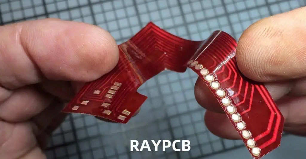
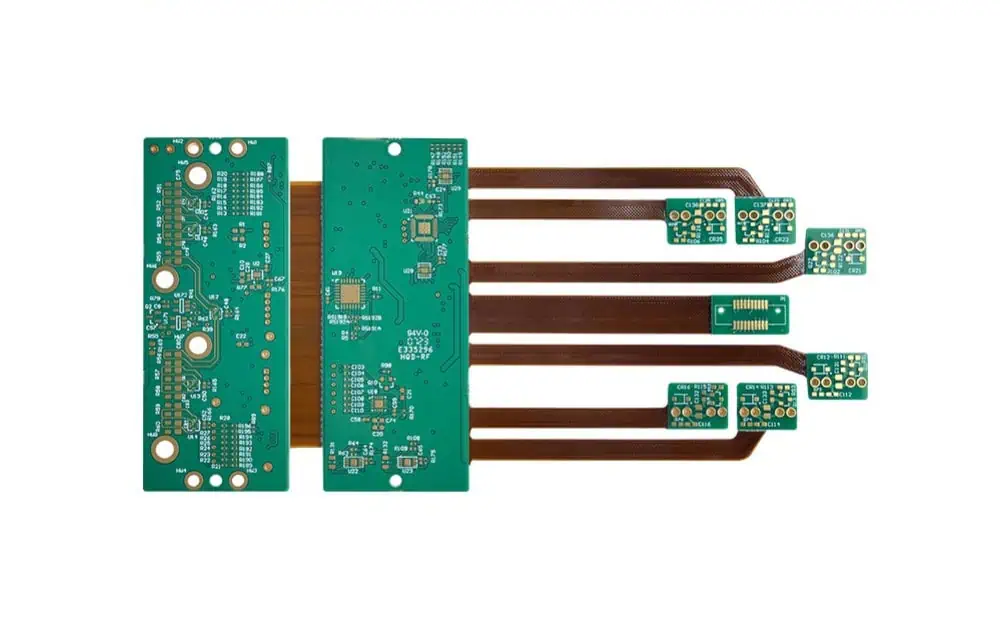
Rigid-Flex PCBs (Printed Circuit Boards) have revolutionized the electronics industry by combining the best features of both rigid and flexible circuits. These innovative boards offer a unique solution for complex electronic designs, providing flexibility and durability in a single package. In this comprehensive guide, we’ll explore the intricate manufacturing processes behind Rigid-Flex PCBs, their characteristics, applications, and common design mistakes to avoid.
What Are Rigid-Flex PCBs?
Imagine a circuit board that can bend and twist without breaking. That’s a Rigid-Flex PCB! It’s like having a regular circuit board (the rigid part) connected to a flexible, bendable circuit (the flex part) all in one piece.
Key Features of Rigid-Flex PCBs:
Flexibility: They can bend and fold to fit tight spaces
Durability: Less likely to break under stress
Space-Saving: No need for bulky connectors between board sections
Weight Reduction: Lighter than traditional PCB setups
Where Are They Used?
Rigid-Flex PCBs are the unsung heroes in many devices we use daily. You’ll find them in:
Using precise laser cutting, we trim away excess material around the flex sections. This defines where the board can bend and where it stays rigid.
12. Testing, Testing, 1-2-3
Finally, we put the board through rigorous testing:
Checking all connections
Testing the overall function of the circuit
Making sure it bends where it should without breaking
Rigid-Flex PCB Designs: Shapes and Styles
Rigid-Flex PCBs come in various designs to suit different needs:
Flex to Install: Shipped flat, bends for installation
Flex to Flex: Multiple flex circuits connecting rigid sections
Rigid-Flex: A mix of rigid and flex layers in one board
Sculptured Flex: Varying thickness in different areas
Bookbinder: Rigid sections connected by a flexible “spine”
Top 10 Design Mistakes to Avoid
When creating Rigid-Flex PCBs, watch out for these common pitfalls:
Poor Layer Planning: Can lead to a board that falls apart
Bending Too Much: Overly tight bends can break circuits
Misaligned Layers: Causes connection failures
Skimping on Copper: Too little copper in flex areas leads to tears
Forgetting About Heat: Overlooking thermal management causes performance issues
Misplaced Vias: Putting connection points in the wrong spots reduces reliability
Using the Wrong Materials: Some materials don’t flex well long-term
Incorrect Trace Routing: Traces in the wrong direction can break when flexed
Too Much Rigidity: Defeats the purpose of a flex design
Overly Complex Designs: Can be difficult or impossible to manufacture
Wrapping Up
Rigid-Flex PCBs are marvels of modern electronics. They allow us to create smaller, lighter, and more durable devices than ever before. From the initial material selection to the final testing, each step in the manufacturing process is crucial in creating these versatile circuit boards.
As technology continues to advance, Rigid-Flex PCBs will play an increasingly important role. They’re pushing the boundaries of what’s possible in electronics, finding their way into ever more compact and complex devices.
Understanding how these boards are made not only gives us appreciation for the devices we use daily but also inspires future innovations. Who knows? The next groundbreaking electronic device might just be made possible by a cleverly designed Rigid-Flex PCB!
In the world of DIY electronics and rapid prototyping, the ability to produce custom Printed Circuit Boards (PCBs) quickly and cost-effectively is invaluable. One innovative approach that has gained popularity among hobbyists and small-scale manufacturers is modding an inkjet printer for PCB production. This article will explore the process, benefits, and challenges of converting a standard inkjet printer into a PCB manufacturing tool.
Understanding the Basics
What is PCB Production?
PCB production is the process of creating circuit boards that mechanically support and electrically connect electronic components using conductive tracks, pads, and other features etched from copper sheets laminated onto a non-conductive substrate.
The inkjet PCB production method involves using a modified inkjet printer to directly print resist patterns onto copper-clad boards, which are then etched to create the final PCB.
Why Mod an Inkjet for PCB Production?
Advantages
Cost-effective for small-scale production
Rapid prototyping capabilities
Accessibility for hobbyists and small businesses
Customization potential
Environmentally friendly (less waste)
Limitations
Limited resolution compared to professional methods
Size constraints based on printer dimensions
Not suitable for high-volume production
Potential for inconsistent results
Choosing the Right Inkjet Printer
Printer Selection Criteria
When selecting an inkjet printer for PCB production, consider the following factors:
Print resolution
Ink type compatibility
Paper feed mechanism
Printer age and availability of parts
Cost
Recommended Printer Models
Printer Model
Resolution (dpi)
Ink Compatibility
Paper Feed
Estimated Cost ($)
Epson Stylus C88
5760 x 1440
Pigment
Rear
150-200
Canon PIXMA iP7220
9600 x 2400
Dye/Pigment
Rear/Front
100-150
HP Deskjet 1000
1200 x 1200
Dye
Rear
50-100
Brother MFC-J470DW
6000 x 1200
Dye/Pigment
Rear/Front
80-130
The Modding Process
Step 1: Disassembling the Printer
Remove the outer casing
Identify key components (print head, ink cartridges, paper feed mechanism)
Document the disassembly process for reassembly
Step 2: Modifying the Paper Feed Mechanism
Remove or adjust paper sensors
Modify the paper tray to accommodate PCB substrates
Adjust roller tension for thicker materials
Step 3: Adapting the Print Head
Clean the print head thoroughly
Modify ink channels for conductive ink (if necessary)
Modding an inkjet printer for PCB production offers an accessible and cost-effective solution for hobbyists and small-scale manufacturers. While it has limitations compared to professional methods, the ability to rapidly prototype and produce custom PCBs in-house can be invaluable. As technology continues to advance, we can expect to see further improvements in this DIY approach to PCB manufacturing.
Frequently Asked Questions (FAQ)
1. Is modding an inkjet printer for PCB production legal?
Modding your own inkjet printer for personal use is generally legal. However, it’s important to note that this modification may void the printer’s warranty. If you plan to use the modded printer for commercial purposes, be sure to check local regulations and obtain any necessary certifications.
2. What type of ink should I use for PCB production?
For PCB production, you’ll need either conductive ink or etchant resist ink, depending on your preferred method. Conductive inks typically contain silver or copper nanoparticles, while etchant resist inks are often UV-curable or solvent-resistant. It’s crucial to choose an ink that’s compatible with your printer and substrate material.
3. How does the resolution of a modded inkjet printer compare to professional PCB production methods?
A modded inkjet printer typically achieves resolutions between 0.1mm and 0.3mm, which is suitable for many hobbyist and prototype projects. Professional PCB production methods, such as photolithography, can achieve resolutions below 0.1mm. While a modded inkjet may not match professional-grade equipment, it can produce functional PCBs for many applications.
4. Can I produce multi-layer PCBs with a modded inkjet printer?
Yes, it is possible to produce multi-layer PCBs with a modded inkjet printer, but it requires additional steps and precision. You’ll need to print each layer separately, carefully align them using registration marks, and use techniques like via-plating to connect the layers. While more challenging than single-layer boards, multi-layer production is achievable with practice and patience.
5. What are the main challenges in modding an inkjet printer for PCB production?
The main challenges include:
Modifying the paper feed mechanism to handle rigid PCB substrates
Adapting the ink system for conductive or resist inks
Achieving consistent print quality and resolution
Maintaining proper alignment for multi-layer boards
Dealing with potential clogging issues due to specialized inks
Overcoming these challenges requires patience, experimentation, and a willingness to troubleshoot and refine your setup.
Debugging Printed Circuit Boards (PCBs) is an essential skill for electronics engineers and hobbyists alike. When your carefully designed circuit doesn’t work as expected, systematic debugging techniques can help you identify and resolve issues quickly and efficiently. This comprehensive guide will walk you through everything you should know about PCB debugging, from basic concepts to advanced techniques.
Introduction to PCB Debugging
PCB debugging is the process of identifying and resolving issues that prevent a circuit from functioning as intended. It requires a systematic approach, patience, and a deep understanding of electronics principles. Effective debugging can save time, reduce costs, and improve the overall quality of electronic products.
Common PCB Issues
Understanding common PCB issues can help you quickly identify potential problems during the debugging process.
Identify open or short circuits in high-speed lines
Electron Microscopy
Examine solder joint quality at a microscopic level
Investigate component failure modes
Documenting and Reporting Bugs
Proper documentation is crucial for tracking progress and preventing future issues.
Bug Report Template
Field
Description
Issue ID
Unique identifier for the bug
Description
Clear, concise explanation of the problem
Steps to Reproduce
Detailed procedure to replicate the issue
Expected Behavior
What should happen when working correctly
Actual Behavior
What actually happens
Environment
Hardware version, software version, test conditions
Severity
Impact of the bug on system functionality
Attachments
Relevant screenshots, waveforms, or log files
Prevention Strategies for Future Designs
Learning from debugging experiences can help prevent issues in future designs.
Design for Testability (DFT) Principles
Include test points for critical signals
Implement boundary scan (JTAG) capabilities
Design modular circuits for easier isolation of problems
Use clear silkscreen labels for components and test points
Frequently Asked Questions
1. What is the first thing I should do when debugging a PCB?
The first step in PCB debugging should always be a thorough visual inspection. This non-invasive technique can quickly reveal many common issues such as solder bridges, missing components, or incorrect component placement. Use a magnifying glass or microscope to examine the board carefully, paying attention to solder joints, component orientation, and any signs of physical damage. This initial step can save significant time by identifying obvious problems before moving on to more complex electrical tests.
2. How can I debug intermittent issues in my PCB?
Debugging intermittent issues can be challenging, but here are some strategies:
Environmental Testing: Subject the PCB to various temperatures, humidity levels, or vibrations to trigger the issue.
Long-term Monitoring: Use data logging tools to capture signals over extended periods.
Stress Testing: Run the system at maximum load or clock speeds to exacerbate potential issues.
Signal Probing: Use oscilloscopes or logic analyzers with trigger functions to capture the moment when the issue occurs.
Power Supply Analysis: Monitor power rails for glitches or dropouts that might cause intermittent behavior.
Remember, patience and systematic testing are key when dealing with intermittent problems.
3. What are some common mistakes to avoid when debugging PCBs?
Common mistakes in PCB debugging include:
Jumping to Conclusions: Avoid assuming you know the problem without proper investigation.
Neglecting ESD Precautions: Always use proper ESD protection to avoid damaging sensitive components.
Poor Documentation: Failing to document steps taken and observations made during debugging.
Changing Multiple Things at Once: This can make it difficult to identify which change solved the problem.
Overlooking Power Issues: Always verify power supply voltages and currents first.
Ignoring Thermal Considerations: Heat-related issues can cause intermittent problems that are hard to diagnose.
Forgetting Signal Integrity: In high-speed designs, signal integrity issues can cause subtle problems.
4. How do I debug a PCB with no schematic or documentation?
Debugging a PCB without documentation is challenging but not impossible. Here’s an approach:
Create a Schematic: Trace the PCB connections and draw a schematic as you go.
Identify Key Components: Look up part numbers to understand the circuit’s function.
Power Analysis: Identify power input and key voltage rails.
Signal Tracing: Use a combination of visual inspection and electrical measurements to understand signal flow.
Functional Blocks: Try to identify and isolate functional blocks within the circuit.
Reverse Engineering Tools: Consider using PCB visualization software or X-ray imaging for complex boards.
Online Research: Look for similar products or designs that might provide clues.
Remember, this process can be time-consuming, so patience is crucial.
5. What tools are essential for a beginner in PCB debugging?
For a beginner in PCB debugging, these tools are essential:
Multimeter: For basic voltage, current, and resistance measurements.
Magnifying Glass or USB Microscope: For detailed visual inspection.
Soldering Iron: For basic rework and modifications.
Oscilloscope: Even a basic model can provide valuable insight into signal behavior.
Logic Probe: A simple tool for checking digital signal states.
Power Supply: For powering the circuit under controlled conditions.
Tweezers and Small Tools: For handling small components and probing tight spaces.
ESD Protection: Anti-static mat and wrist strap to prevent electrostatic damage.
As you gain experience, you can add more advanced tools like logic analyzers or thermal cameras to your toolkit.
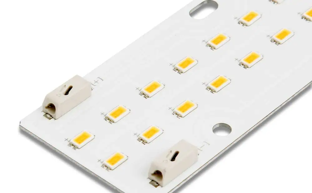
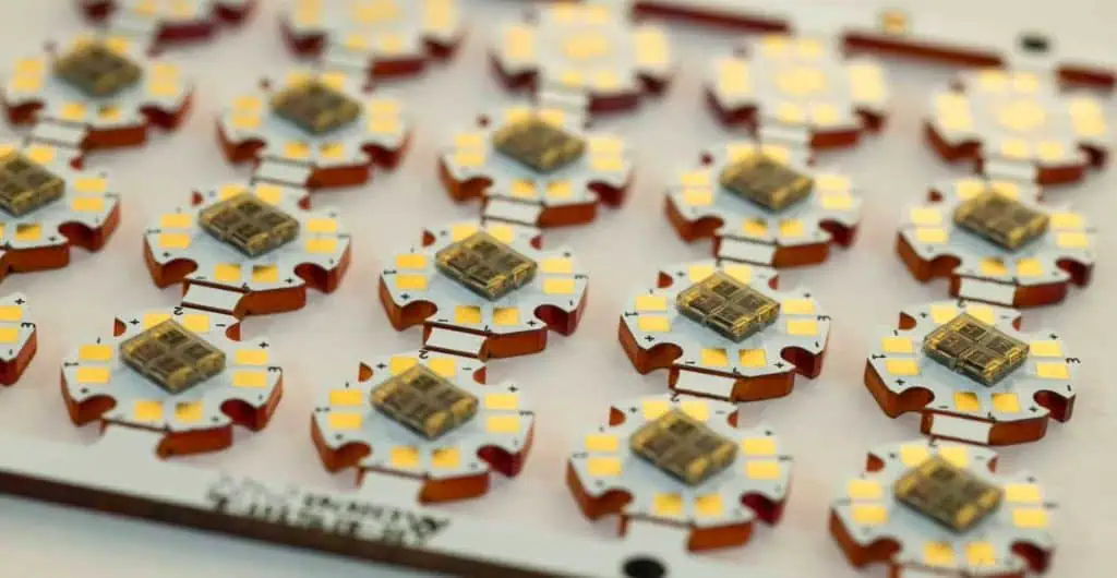
LED grow lights have revolutionized indoor farming and horticulture, offering energy-efficient and customizable lighting solutions for plants. At the heart of these innovative lighting systems lies the printed circuit board (PCB), which serves as the foundation for mounting and connecting the LED components. This comprehensive guide delves into the intricate world of LED grow light PCB manufacturing, covering everything from design considerations to material selection and production processes.
Understanding LED Grow Lights
Before diving into the manufacturing process, it’s essential to understand the basics of LED grow lights and their importance in modern agriculture.
What are LED Grow Lights?
LED grow lights are specialized lighting fixtures designed to stimulate plant growth by emitting light at specific wavelengths that plants need for photosynthesis and other biological processes. These lights offer several advantages over traditional lighting solutions:
Energy efficiency
Longer lifespan
Reduced heat output
Customizable light spectra
Compact design
The Role of PCBs in LED Grow Lights
Printed Circuit Boards (PCBs) play a crucial role in LED grow lights by:
Providing a stable mounting surface for LEDs
Facilitating electrical connections between components
Managing heat dissipation
Enabling complex circuit designs for advanced features
Ensuring consistent light output and performance
PCB Basics for LED Grow Lights
Types of PCBs Used in LED Grow Lights
LED grow light PCBs come in various types, each with its own set of advantages and applications:
X-ray Inspection: For checking internal layers and hidden solder joints
Quality Control and Testing
Ensuring the quality and reliability of LED grow light PCBs is crucial for long-term performance and customer satisfaction.
Quality Control Measures
Incoming Material Inspection: Verify the quality of raw materials before production
In-Process Inspections: Regular checks during each stage of manufacturing
Automated Optical Inspection (AOI): Detect defects in solder mask, silkscreen, and copper patterns
X-ray Inspection: Examine internal layers and hidden solder joints
Electrical Testing: Verify circuit continuity and isolation
Performance Testing
Thermal Cycling: Test PCB performance under varying temperature conditions
Vibration Testing: Ensure durability in high-vibration environments
Humidity Testing: Verify resistance to moisture ingress
Light Output Measurement: Confirm desired intensity and spectral distribution
EMI/EMC Testing: Check for electromagnetic interference and compatibility
Cost Considerations
Understanding the factors that influence the cost of LED grow light PCB manufacturing can help in making informed decisions and optimizing production expenses.
Factors Affecting PCB Manufacturing Costs
Factor
Impact on Cost
Considerations
Board Size
Larger boards increase cost
Optimize design for efficient space usage
Layer Count
More layers increase cost
Balance complexity with layer count
Material Selection
Specialty materials cost more
Choose materials based on performance requirements
Copper Weight
Heavier copper increases cost
Select appropriate weight for current and thermal needs
Surface Finish
Some finishes are more expensive
Consider durability and assembly method
Minimum Feature Size
Smaller features increase cost
Design with manufacturability in mind
Order Quantity
Larger quantities reduce per-unit cost
Consider production volume and inventory management
Turnaround Time
Faster production increases cost
Plan production schedule to balance cost and lead time
Cost Optimization Strategies
Design for Manufacturability (DFM): Optimize designs to reduce complexity and improve yield
Panel Utilization: Maximize the number of PCBs per panel to reduce waste
Material Selection: Choose cost-effective materials that meet performance requirements
Volume Production: Leverage economies of scale for larger production runs
Supplier Relationships: Develop long-term partnerships with PCB manufacturers for better pricing
Future Trends in LED Grow Light PCB Manufacturing
As technology advances, several trends are shaping the future of LED grow light PCB manufacturing:
Increased Automation: Greater use of robotics and AI in PCB production
Advanced Materials: Development of new substrate materials with improved thermal and electrical properties
3D Printing: Exploration of additive manufacturing techniques for PCB production
IoT Integration: Incorporation of sensors and connectivity features in LED grow light PCBs
Sustainable Manufacturing: Focus on eco-friendly materials and energy-efficient production processes
Miniaturization: Trend towards smaller, more efficient LED grow light designs
Flexible and Stretchable PCBs: Development of adaptable PCB solutions for unique grow light applications
Frequently Asked Questions
1. What is the best PCB material for LED grow lights?
The best PCB material for LED grow lights depends on the specific requirements of your application. For high-power LED grow lights that generate significant heat, metal-core PCBs (MCPCBs) made with aluminum substrates are often the preferred choice due to their excellent thermal management properties. For lower-power applications or where cost is a primary concern, FR-4 boards with additional thermal management features may be suitable.
2. How do I ensure proper thermal management in LED grow light PCBs?
Proper thermal management in LED grow light PCBs can be achieved through several strategies:
Use of metal-core PCBs or boards with high thermal conductivity
Incorporation of thermal vias to improve heat transfer
Optimal component placement to distribute heat evenly
Integration of heat sinks or cooling systems
Selection of LEDs with good thermal properties
Proper thermal design and simulation during the PCB layout phase
3. What surface finish is recommended for LED grow light PCBs?
The choice of surface finish depends on factors such as assembly method, environmental conditions, and cost considerations. Some popular options include:
ENIG (Electroless Nickel Immersion Gold): Offers good solderability and protection against oxidation
HASL (Hot Air Solder Leveling): Cost-effective option with good solderability
Looking for reliable low volume PCB solutions? Whether you’re developing prototypes, testing new designs, or serving niche markets, low volume PCB manufacturing offers the perfect balance of cost-effectiveness and flexibility for your electronic projects.
What is Low Volume PCB Manufacturing?
Low volume PCB manufacturing refers to the production of printed circuit boards in smaller quantities, typically ranging from 10 to 1,000 units. This approach bridges the gap between prototype development and mass production, making it ideal for businesses that need quality PCBs without committing to large-scale orders.
Why Choose Low Volume PCB Production?
Cost-Effective Solution for Small Orders
Low volume PCB production eliminates the need for massive upfront investments. You only pay for what you need, making it perfect for:
Startups with limited budgets
Research and development projects
Custom electronics applications
Market testing initiatives
Faster Time-to-Market
Unlike high-volume manufacturing that requires extensive setup time, low volume PCB production offers:
When Should You Consider Low Volume PCB Manufacturing?
Perfect Scenarios for Low Volume PCB Orders
Prototyping and Testing Low volume PCB manufacturing excels when you need to validate designs before full-scale production. This approach allows you to identify potential issues early and make necessary adjustments without significant financial impact.
Customized Projects For specialized applications requiring unique specifications, low volume PCB production offers the flexibility to create tailored solutions without the constraints of mass production minimums.
Niche Market Products If your target market has limited demand, low volume PCB manufacturing ensures you don’t overproduce and tie up capital in excess inventory.
Iterative Design Development When your PCB design is still evolving, low volume production enables cost-effective iterations and improvements without the burden of large-scale changes.
Industries That Benefit from Low Volume PCB
Medical Devices: Specialized equipment with strict regulatory requirements
Aerospace: High-reliability applications with limited production runs
Industrial Automation: Custom control systems and specialized machinery
Conclusion: Maximize Your Success with Low Volume PCB
Low volume PCB manufacturing offers an ideal solution for businesses seeking quality, flexibility, and cost-effectiveness in their electronic projects. Whether you’re developing innovative products, serving specialized markets, or testing new concepts, choosing the right low volume PCB manufacturer can significantly impact your success.
The key to maximizing your low volume PCB investment lies in selecting an experienced manufacturer who understands your unique requirements and can deliver consistent quality at competitive prices. With proper planning, clear communication, and strategic partnerships, low volume PCB manufacturing becomes a powerful tool for innovation and growth.
Ready to explore low volume PCB solutions for your project? Contact experienced manufacturers who specialize in small-batch production and can provide the expertise, quality, and service you need to bring your electronic designs to life efficiently and cost-effectively.