Are you looking for reliable PCB clone and PCB copy services? When you have a physical electronic circuit board but lack the original design files, our professional PCB clone service provides the perfect solution. Whether you need PCB copy for obsolete boards or circuit duplication for production scaling, we deliver precision results.

What is PCB Clone and PCB Copy Technology?
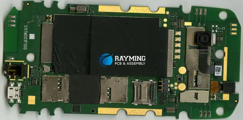
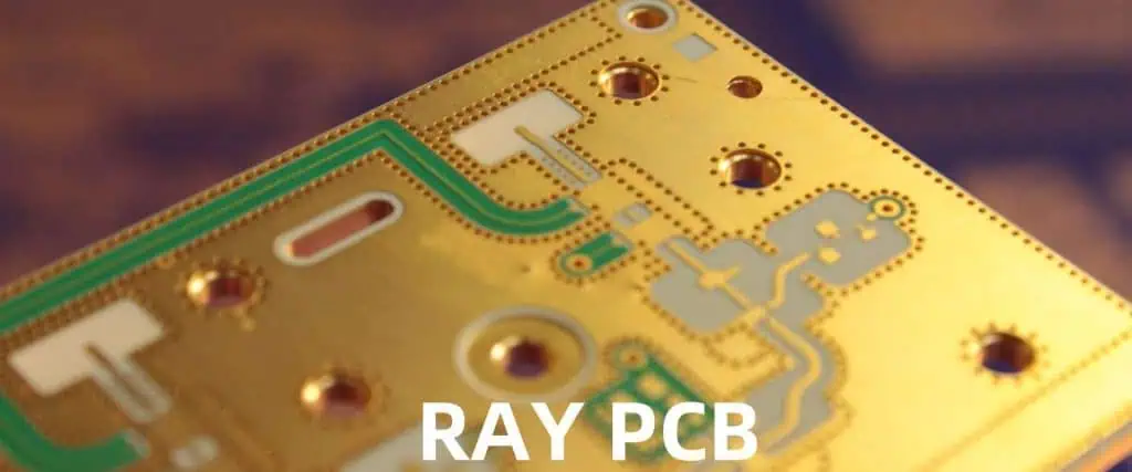
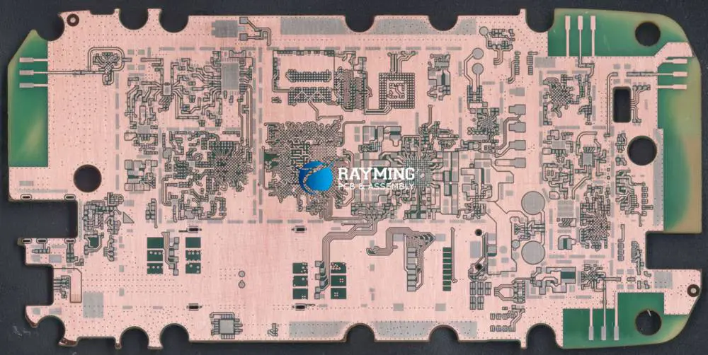
PCB clone, also known as PCB copy or PCB duplication, is an advanced reverse engineering technology that creates exact replicas of existing printed circuit boards. Our PCB clone process analyzes your original board and produces identical copies without requiring original design files or Gerber drawings.
Key Features of Our PCB Clone Service:
- Complete PCB copy from physical samples
- Schematic diagram restoration
- Bill of Materials (BOM) generation
- Gerber file creation
- Component identification and sourcing
Why Choose PCB Clone Over Traditional Design?

Cost-Effective PCB Copy Solutions
Traditional PCB design from scratch involves significant costs including prototype development, testing, and design optimization. Our PCB clone service eliminates these expenses by reverse-engineering existing boards. PCB copy technology reduces development time and costs by up to 70% compared to original design processes.
Fast Turnaround PCB Clone Process
Our streamlined PCB clone workflow ensures rapid delivery:
- Sample Analysis: Send photos of your board for initial PCB copy assessment
- Quotation: Receive detailed pricing for your PCB clone project
- Sample Submission: Ship physical samples for precise PCB copy analysis
- Reverse Engineering: Our experts perform comprehensive PCB clone procedures
- Deliverables: Receive complete files including Gerber, schematics, and BOM
Professional PCB Copy Applications
Legacy System Replacement
When original manufacturers discontinue support, PCB clone services become essential. Our PCB copy expertise helps maintain critical systems in:
- Industrial automation equipment
- Medical devices
- Aerospace applications
- Telecommunications infrastructure
Production Scaling Through PCB Clone
Manufacturers use PCB copy services to scale production without licensing fees. Our PCB clone process enables:
- Rapid prototyping
- Cost reduction
- Supply chain independence
- Quality improvement opportunities
Advanced PCB Clone Techniques

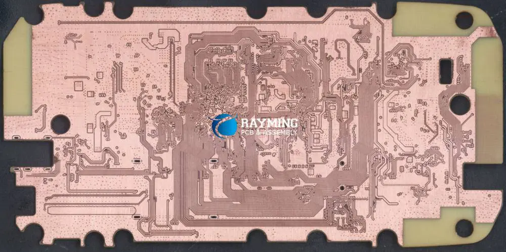
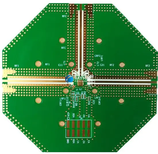
Multi-Layer PCB Copy Capabilities
Our PCB clone service handles complex multi-layer boards with precision. Advanced PCB copy techniques include:
- Layer-by-layer analysis
- Via mapping and reconstruction
- Trace routing optimization
- Component placement accuracy
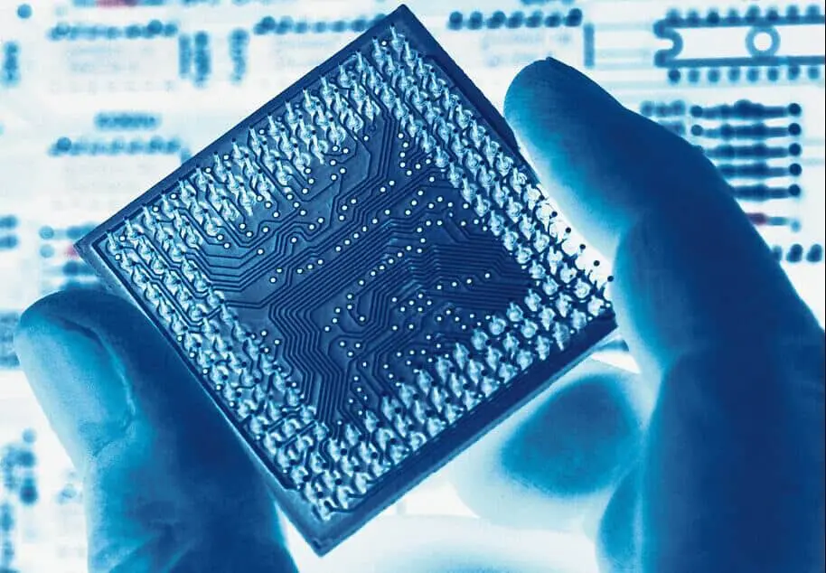
Intelligent Component Analysis
Modern PCB clone projects often involve microcontrollers and programmable devices. Our PCB copy service includes:
- Firmware extraction (where legally permissible)
- IC programming analysis
- Memory dumping procedures
- Code reverse engineering
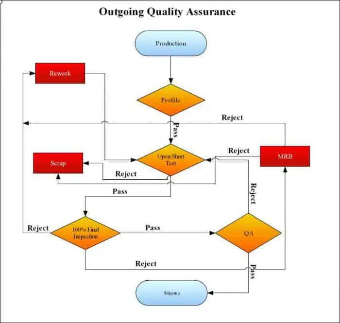
Quality Assurance in PCB Clone Projects
Precision PCB Copy Standards
Every PCB clone project undergoes rigorous quality control:
- Dimensional accuracy verification
- Electrical continuity testing
- Component value confirmation
- Performance validation
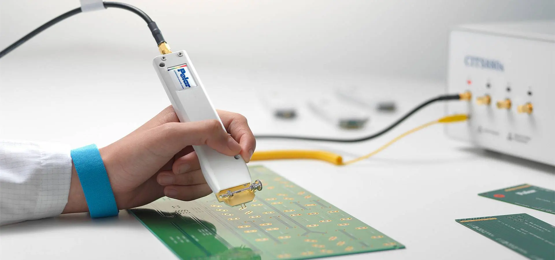
Testing and Validation
Our PCB copy process includes comprehensive testing:
- Functional verification
- Signal integrity analysis
- Thermal performance assessment
- Reliability testing
Industries Served by PCB Clone Services

Automotive PCB Copy
The automotive industry relies on PCB clone services for:
- ECU replacement modules
- Legacy vehicle support
- Performance modifications
- Cost optimization
Medical Device PCB Clone
Healthcare equipment manufacturers use PCB copy for:
- Life-critical system maintenance
- Regulatory compliance
- Obsolescence management
- Cost-effective repairs
Consumer Electronics PCB Copy
Consumer product manufacturers leverage PCB clone for:
- Product improvement
- Cost reduction
- Feature enhancement
- Market adaptation
Technical Specifications for PCB Clone Projects

PCB Copy Capabilities
- Board thickness: 0.2mm – 6.0mm
- Layer count: 1-30 layers
- Minimum trace width: 0.075mm
- Component density: High-density support
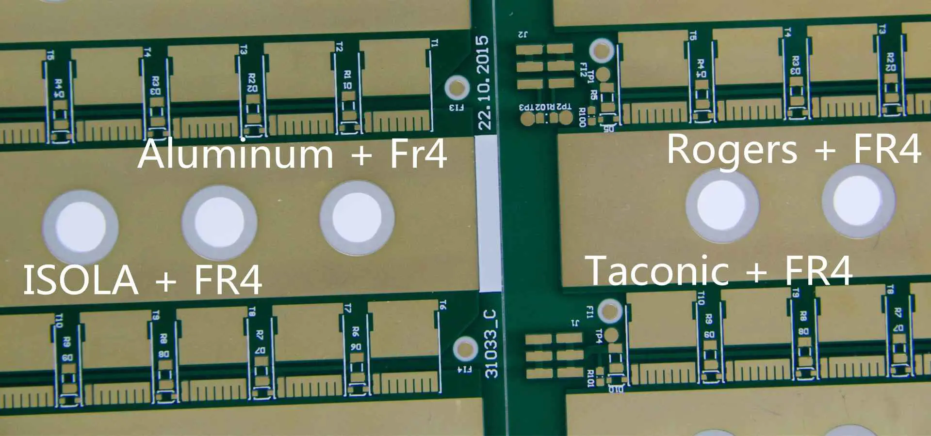
- Material types: FR4, Rogers, polyimide, aluminum
PCB Clone Accuracy Standards
- Dimensional tolerance: ±0.05mm
- Component placement accuracy: ±0.025mm
- Electrical performance: 100% functional equivalence
- Material matching: Exact or equivalent specifications
Getting Started with PCB Clone Services
PCB Copy Consultation Process
- Initial Assessment: Submit clear photos of your PCB for preliminary PCB clone evaluation
- Technical Review: Our engineers analyze complexity and provide PCB copy recommendations
- Proposal: Detailed quotation including timeline and deliverables
- Sample Analysis: Physical board examination for precise PCB clone specifications
- Project Execution: Professional PCB copy implementation with regular updates
PCB Clone Documentation Package
Every completed PCB copy project includes:
- Complete Gerber file set
- Drill files and NC data
- Pick and place files
- Bill of Materials (BOM)
- Assembly drawings
- Test procedures
Cost Factors in PCB Clone Projects
PCB Copy Pricing Considerations
PCB clone costs depend on several factors:
- Board complexity (layer count, component density)
- Component identification requirements
- Firmware analysis needs
- Documentation depth
- Quantity requirements
Value Proposition of PCB Clone
Compared to original design, PCB copy services offer:
- 60-80% cost reduction
- 70% faster time-to-market
- Reduced risk through proven designs
- Immediate availability
Advanced PCB Clone Technologies
High-Frequency PCB Copy
Specialized PCB clone techniques for RF and microwave applications:
- Impedance matching preservation
- Signal integrity maintenance
- Material property analysis
- Performance optimization
Flexible PCB Clone Services
Our PCB copy capabilities extend to flexible circuits:
- Flex-rigid board analysis
- Bend radius optimization
- Connection reliability
- Dynamic application support
Quality Management in PCB Clone
ISO Standards Compliance
Our PCB clone processes follow international standards:
- ISO 9001:2015 quality management
- IPC standards compliance
- RoHS and REACH compliance
- Industry-specific certifications
Continuous Improvement
We enhance our PCB copy methodologies through:
- Technology upgrades
- Process optimization
- Customer feedback integration
- Industry best practices adoption
Intellectual Property Considerations

Ethical PCB Clone Practices
Our PCB copy services operate within legal frameworks:
- Customer ownership verification
- Reverse engineering legality
- Confidentiality agreements
- Ethical business practices
Protecting Your PCB Clone Investment
We safeguard your PCB copy projects through:
- Secure data handling
- Non-disclosure agreements
- Proprietary information protection
- Long-term support commitments
Contact Us for PCB Clone Services
Ready to start your PCB clone or PCB copy project? Our expert team provides comprehensive circuit board duplication services with guaranteed quality and fast delivery. Contact us today for a free consultation and discover how our PCB clone expertise can solve your electronic design challenges.
Email: sales@raypcb.com Services: Complete PCB clone and PCB copy solutions Specialties: Multi-layer boards, high-frequency circuits, legacy system replacement
Transform your electronic projects with professional PCB clone and PCB copy services that deliver precision, reliability, and cost-effectiveness.