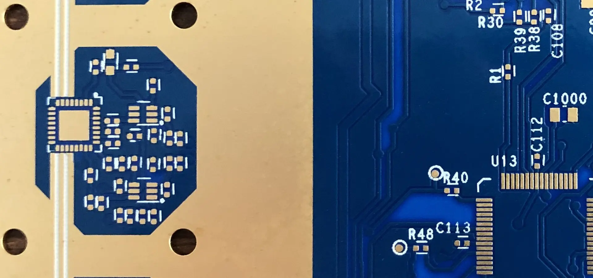
Supporting the military is something RayMing is very proud of, and we were contracted to assemble a PCB for use in a military communications application. The RF prototype PCB assembly used Rogers 4350B material, and the board required surface mount technology for the double-sided assembly that featured 250 placements. Board specs included 3 layers, standard vias, and 1 panelization. Final measurements came to 8 x 5.75 in. We performed final testing using automated optical inspections and x-ray inspection before delivering product to the customer.
Introduction
Rogers RO4350B laminates are widely used for manufacturing high frequency PCBs for defense and aerospace applications like radars, electronic warfare systems, satellite communications, etc. This high performance PCB material enables circuits to operate reliably at microwave and mm-wave frequencies beyond 10 GHz.
However, assembling PCBs using RO4350B substrates requires special considerations during fabrication, component selection and assembly processes owing to its unique properties. This article provides guidelines on how to assemble RO4350B PCBs for mission-critical military applications.
RO4350B is a glass reinforced fluoropolymer composite circuit board material designed for exacting microwave and mm-wave circuit needs. Here are some of its key properties:
RO4350B’s electrical and mechanical attributes make it suitable for aerospace RADARs, satellite communication, electronic warfare systems and radio communications.
Design Considerations
The PCB layout for an RO4350B board destined for military usage must account for the following:
Controlled Impedance
Maintain tight impedance control over traces and match to RF IC terminations
RF Shielding
Incorporate adequate shielding enclosures for emission control
Minimal Passives
Limit passive components to reduce losses at high frequencies
RF Transitions
Carefully design components/connectors interfaces
Thermal Management
Use thermal vias and/or metal backing to spread heat
Reliability Testing
Subject prototype to thermal cycling, vibration and shock tests
PCB Fabrication Process
RO4350B PCBs require specialized fabrication to meet military specifications:
Material – Use RO4350B laminates from Rogers or equivalent suppliers
Layer Count – Typical stackups have 4 to 32 layers depending on complexity
Dielectrics – Combination of RO4350 prepregs and bondplies
Trace width – RF traces down to 3 mils line with 3 mil spacing
Hole walls – Copper plated through holes with 1 oz copper
Surface finish – Immersion silver or ENIG surface finish
Testing – Full electrical testing and quality inspection per IPC standards
Component Selection
The active and passive components used on the PCB assembly must also conform to RF application needs:
RF Transistors
Gallium arsenide (GaAs) RF power transistors with operating frequency > 10 GHz
Power Amplifiers
GaN or GaAs MMIC power amplifiers from suppliers like Qorvo, Microchip, etc.
RF Connectors
High frequency SMP, SMPM, SSMP connectors rated for microwave bands
Passive Components
Chip resistors, capacitors and inductors with tight tolerances rated for high frequency use
EMI Suppression
Multi-layer ceramic capacitors, ferrite chip beads for noise filtering
LED lighting has transformed how we illuminate our homes, offices, streets and virtually every aspect of our lives. LED bulbs and fixtures provide huge advantages over traditional incandescent and CFL lighting in terms of efficiency, lifetime, durability and lighting quality. This article looks at some of the best LED lighting products across various categories that consumers can choose to buy for their lighting needs.
Dimmable – Dimmable LED lights allow adjusting brightness levels.
Specialty – Select specialty LEDs for path lighting, accent lighting, under cabinet, etc.
Indoor/Outdoor – Ensure IP-rating for outdoor LED fixtures for moisture resistance.
Safety – LED products must meet safety standards like UL/ETL, FCC.
Brand – Reputable brands assure quality and performance.
Warranty – Multi-year warranties cover LED lifespan claims.
Budget – LED prices range from value packs to premium smart fixtures.
Best LED Light Bulbs
LED light bulbs have become the top choice for energy efficient, long lasting and high quality lighting for homes and businesses. Here are some of the best LED bulbs:
Philips LED Bulbs
Philips offers an extensive range of LED bulbs including clear, frosted, globe, candle, reflector and 3-way models. Great value for money with good color quality and 10-year lifespan.
Key Features:
800-2000 Lumens brightness options
2700K-5000K CCT range
90+ CRI for vivid colors
10 year lifespan
ENERGY STAR certified
Cree Lighting LED Bulbs
With 90+ CRI and soft lighting, Cree’s wide assortment of LED bulbs deliver beautiful illumination. 5000K-6500K Tunable White models allow adjusting the color.
Key Features:
800-1600 Lumens output
Available in standard and candelabra bases
High efficiency – 100 Lumens per Watt
Changeable color temperature
Dimmable
GE LED Light Bulbs
A household lighting brand, GE offers LED bulbs in all common shapes with a range of brightness and color temperatures. Affordable pricing with good 10-year lifespan.
Key Features:
450-1600 Lumens models
Standard and decorative options
2700K/3000K/5000K CCT
Up to 90 CRI
Omnidirectional and directional bulbs
Rated for 25,000 hours
Sylvania LED Bulbs
Sylvania makes a wide range of replacement LED bulbs for homes and businesses that deliver crisp, bright light using latest LED technology for efficiency and longevity.
Smart LED bulbs can be remotely controlled and scheduled via smartphone apps over Wi-Fi/Bluetooth. Here are the top options:
Philips Hue Smart Bulbs
Philips Hue is the most popular smart LED lighting system. The color-changing A19 bulbs can recreate millions of shades. Controls lights from anywhere.
Key Features:
800 Lumens brightness
16 million colors
App and voice control
Automation and schedules
Works with Alexa, Google Home etc.
Create lighting scenes
Sync with movies and music
C by GE C-Life Smart Multicolor Bulbs
These smart C-Life bulbs from GE allow changing any shade from soft white to daylight to colored lighting. Offers both Bluetooth and Wi-Fi connectivity.
Key Features:
800 Lumens output
Tunable shades and colors
Scheduling and automation
Voice control integration
Group control of multiple bulbs
Energy monitoring
LIFX Smart Wi-Fi LED Bulbs
LIFX bulbs are packed with features including millions of colors, effects, schedules and integrations. No hub required with direct Wi-Fi setup. Vivid colors and brightness.
Key Features:
1100 Lumens
16 million colors and tones
Effects like candle flicker
Scheduling and automation
Apps for iOS, Android
Works with Alexa, Google Assistant
Kids friendly scenes
TP-Link Kasa Smart KL130
Budget-friendly smart bulbs from TP-Link offering 16 million colors, scheduling, grouping, voice control and energy usage monitoring. Reliable performance.
Key Features:
800 Lumens brightness
Tunable white to full colors
Scheduling and timers
Voice control via Alexa, Google
Create scenes and groups
Monitor energy usage
No hub required
Best LED Recessed Ceiling Lights
Recessed lighting provides even ceiling illumination. Here are top rated LED recessed lighting kits suitable for different room types:
Philips All-in-One 5/6 in. LED Recessed Lighting Kit
Complete recessed lighting kit from Philips with integrated LED module and trim for fast installation. 90+ CRI for vibrant colors.
Key Features:
900-1300 Lumens flux options
90+ CRI
CCT choices: Soft White, Bright White, Daylight
Dimmable
Included integrated LED and trim
Fast installation
Sunco Lighting 5/6 in. Selectable CCT LED Recessed Kit
Affordable recessed lighting kit with selectable 3000K, 4000K and 5000K color temperatures controlled by a simple switch.
Key Features:
1080 Lumens output
3000K/4000K/5000K CCT
Damp location approved
Can be dimmed
Rotatable light for directing beam
Quick installation
Commercial Electric UltraSlim 4 in. LED Recessed Lighting
Commercial Electric offers an ultra-thin recessed lighting kit using state-of-the-art LEDs with 5000K daylight output. Energy saving and long life.
Key Features:
740 Lumens flux
5000K cool daylight
Super slim only 1.5 inches deep
90+ CRI
Dimmable
50,000 hours lifespan
ENERGY STAR certified
Hyperikon 4 Inch LED Recessed Lighting
Versatile recessed lighting kit with adjustable CCT of 3000K, 4000K and 5000K using sliding switch. High cri and lumen output. Low profile design. Damp location rated.
Key Features:
1000 Lumens flux
Slide switch for 3000K/4000K/5000K
90+ CRI with no flicker
Only 1.25 in. depth
Air tight IC housing
Wet location approved
Best LED Landscape Lighting
Outdoor landscape lighting illuminates gardens, yards, pathways and architecture features at night using low-voltage LEDs. Here are top options:
Volt Lyte Landscape LED Lighting Kit
Complete 12V outdoor LED lighting kit with 8 adjustable spotlights, transformers, cables and ground stakes for accent lighting.
Key Features:
8 bright LED spotlights
Adjustable light angles
Warm white 3000K
25 ft. cable, connectors and transformer included
Low voltage safe operation
Automatic shut-off timer
Easy DIY installation
JEMLIGHT 4-Head LED Outdoor Landscape Spotlights
Pack of 4 weatherproof adjustable 12V spotlights producing 300 lumens each. Durable die-cast housing with flood to spot beam control.
Key Features:
4 x 300 lumens spotlights
Warm white 3000K CCT
Die-cast aluminum housing
Adjustable flood to spot beams
IP65 weatherproof rating
Low voltage 12V operation
Stake and screw mounts included
Malibu Low Voltage Landscape Lighting Fixture Kit
Malibu offers versatile lighting kit containing path lights, spot lights, well lights and step lights for accenting gardens, patios, driveways.
Key Features:
6 x 35W LED lights
Warm white and cool white
10W transformer
25 ft low voltage cable
Stakes, mounting screws
Durable UV resistant design
Easy installation
Brilliance LED Buried Well Light
Durable recessed well light allows hiding LED fixture underground with only the light visible for a clean, invisible installation.
Solar powered LED lights harness the sun’s energy during daytime and automatically turn on at night without any wiring. Some top options are:
Sunnest Solar Landscape Spotlights
Bright integrated solar spotlights with adjustable heads and convenient ground stakes. Automatically activate at night. Weather resistant construction.
Key Features:
Built-in mono-crystalline solar panel
400 lumen LED spotlight
Adjustable light angle
IP65 weatherproof rating
Auto on/off at dusk/dawn
Stainless steel housing
Easy installation
Gigalumi Solar Path Lights
Affordable solar LED path lights to illuminate walkways and gardens. The solar panel tops each lamp post charging the Lithium battery. Made from durable materials.
Key Features:
Integrated solar panel
400 lumens output
Warm white 3000K CCT
Durable ABS housing
IP65 waterproofing
Auto dusk to dawn operation
6 hours runtime on full charge
Pack of 6 path lights
Aootek 182 LED Solar Motion Sensor Light
Solar powered LED security light with smart motion and light sensors. Bright illumination activated by movements at night to deter intruders.
Key Features:
Built-in solar panel
Motion and light sensors
180 ultra-bright LEDs
6000K cool white light
120° wide beam angle
IP65 weather resistance
Easy wall or ground installation
SolarGlow Solar Garden Lights
Decorative looking LED lights powered by tiny solar panels. Turn on automatically providing a warm glow. Great for gardens, driveways and landscape lighting applications.
Key Features:
Integrated small solar panel
Warm white 2700K light
Customizable with interchangeable tops
Durable ABS plastic body
Shatterproof polyethylene lens
Auto on/off at night and day
4-6 hours operation
Weatherproof IPX4 rating
Best Smart WiFi LED Light Strips
WiFi controlled LED light strips that can change colors, brightness and effects using smartphone apps are great for accent lighting.
Philips Hue LightStrip Plus Smart LED
Philips Hue Lightstrip Plus offers millions of colors that can be wirelessly controlled via smartphones and voice assistants. High 800 lumen output and 16 million colors. Flexible and cuttable.
Key Features:
Voice control through Alexa, Google Assistant
16 million colors
800 lumens bright output
1M and 2M lengths available
Flexible and cuttable
Adhesive tape backing
Create lighting scenes and schedules
Sync with music and videos
Govee RGBIC WiFi LED Strip Lights
Govee’s WiFi LED strip lights deliver colorful accent lighting with app control and Alexa/Google Assistant voice commands. Multiple modes and effects including music sync.
Key Features:
16 million colors
Works with Alexa and Google Home
App control and scheduling
64 scene modes and music sync
Brightness up to 2200 lumens
16.4 ft reels available
Adhesive backing for easy install
Control multiple strips together
Eve Light Strip – Apple HomeKit
Apple HomeKit compatible LED light strip from Eve Systems providing beautiful, energy efficient accent lighting. Control lighting conveniently using Apple devices and Siri.
Key Features:
HomeKit allows Siri and app control
Energy monitoring and automations
1600 lumens max brightness
Color temperature tuning
6.6 ft length
Weatherproof IP67 construction
Flexible and cuttable strip
Lifx Z TV LED Backlight Strip
Sync Lifx Z TV backlight with the colors on your TV for an immersive viewing experience. Tape it behind any screen. Works with Alexa, Google Assistant and Apple HomeKit.
Key Features:
Voice control through smart speakers
Real-time picture syncing
16 million colors
65 inches strip length
Adheres to back of TV
Setup zones and scenes
Schedule on/off times
Diffused lighting spread
Best LED Shop Lights
led light
Bright, efficient LED shop lights provide high lumen illumination over work benches, storage rooms, garages and other utility areas. Here are top options:
Barrina LED T5 Integrated Single Fixture
4 feet long LED integrated fixture with clear shatterproof cover. Ultra bright 6500 lumens output with energy saving 45W power consumption. Link up to 3 fixtures.
Key Features:
Super bright daylight 6500K
Integrated LED with clear cover
45W power, 6500 lumens
4000K and 5000K options available
120° beam angle
Lightweight aluminum housing
Linkable integrated connectors
Hykolity 4 FT LED Utility Shop Light
Feature packed LED shop light fixture producing 5000 lumens crisp white light. Sensible motion sensor turns on when area is occupied to save power. Linkable and mountable design.
Key Features:
Motion sensor for auto on when occupied
5000K cool white light
Integrated 120° reflector
Sturdy aluminum housing
5000 lumens flux output
40W power consumption
Chain up to 3 lights together
Costway 4 FT LED Shop Light
Versatile plug and play LED shop light with hanging chain hooks. Energy efficient with 800 lumens per tube. Daylight color ideal for work spaces.
Key Features:
Plug in cord – no wiring needed
Two 4 feet T8 tubes
6500K daylight output
800 lumens per tube
Built-in power switch
Pull chains for easy on/off
Hanging hooks provided
Plastic end caps
Lithonia Lighting Shop Light 8-Tube Fixture
Large 8 foot long LED shop light fixture containing (8) double tube sections for extremely bright illumination. Ideal for large work areas.
Key Features:
96″ long fixture
Contains (8) 48″ T8 LED tubes
6000 lumens total light output
Daylight color temperature
120-277V AC voltage range
Clear shatterproof lens
Painted steel housing
Surface mount
Best LED Grow Lights
Specialized LED grow lights provide indoor plants and vegetables the full visible light spectrum they need for nurturing photosynthesis and growth.
Spider Farmer SF-2000 LED Grow Light
The Spider Farmer SF-2000 uses cutting edge LEDs and drivers to deliver intense full spectrum light ideal for indoor cultivation. Excellent PAR and Lumen output.
For small and medium sized grow areas, the high efficiency XS1500 provides the right amount of light intensity for indoor plants at various growth stages.
Powerful and affordable full spectrum LED lamp containing triple-chip 10W LEDs. Ideal for home gardening and commercial horticulture applications.
Key Features:
10W triple-chip LEDs
1000W equivalent HPS replacement
Adjustable hanging height
Full spectrum including UV and IR
High PAR value for growth
90° reflector coverage area
Excellent thermal dissipation
MARS HYDRO TS 600W LED Grow Light
The Mars Hydro TS 600W grow light utilizes advanced LED technology to offer high intensity sunlight-like light for indoor gardening. Robust lamp for seedlings to flowering plants.
Printed circuit boards (PCBs) that operate reliably at high frequencies are critical for applications like 5G, satellites, radars, avionics and other wireless communications systems. Manufacturing such high frequency PCBs requires expertise in specialized materials, stackups, fabrication processes and quality control. This article profiles the top 10 manufacturers of high frequency PCBs based on their capabilities.
1. RayMing Technology
Headquarter Location: Shenzhen, China
RayMing Technology is an expert in high frequency PCB prototyping and volume production using cutting edge fabrication technologies and testing. They manufacture boards up to 24 layers for RF frequencies above 10 GHz such as mmWave antennas, radar systems, satellite communication, electronic warfare and aerospace/defense electronics.
Core Capabilities:
PCB materials including Rogers, Taconic, Arlon for mw and mmWaves
Stackups with signal-power-ground layer sequencing
Industry Segments Served: Defense, avionics, telecom, space, automotive
2. TTM Technologies
Headquarter Location: California, United States
TTM Technologies is among the top high frequency PCB manufacturers in the world headquartered in the United States. They fabricate RF/microwave boards for defense and aerospace applications including radars, electronic warfare systems, satellite communications, telemetry systems etc.
Core Capabilities:
PTFE, ceramic and hydrocarbon based laminates
Complex multilayer and HDI boards
Fine line capabilities down to 2/2 mils
Laser microvias and back drilling
ENIG, immersion silver and IPC coatings
Rigid-flex PCBs
Testing for HF parameters
Industry Segments Served: Defense, aerospace, industrial
3. AT&S
Headquarter Location: Leoben, Austria
AT&S is Europe’s largest high frequency PCB manufacturer serving the automotive, industrial, medical and aerospace sectors. They produce advanced HDI, multilayer and rigid-flex boards capable of over 100 GHz frequencies.
Industry Segments Served: Automotive, industrial, medical, aerospace
4. Compeq Manufacturing
Headquarter Location: Taiwan
Compeq Manufacturing is a leading high frequency PCB manufacturer in Asia. They fabricate boards using FR4, Rogers, Teflon, Polyimide for wireless communication applications up to 77 GHz. Their key expertise is in automotive radar PCBs.
Core Capabilities:
Materials including Rogers 4350, 4003C, TMM 3
Stackups for 77GHz automotive radars
HDI with 2 mil lines and 4 mil microvias
Sequential lamination process
Fine line printing down to 4 mil
Rigid-flex PCBs
IATF 16949 automotive qualified
Industry Segments Served: Automotive, communication
5. Elec & Eltek
Headquarter Location: Taiwan
Elec & Eltek specialize in making high frequency PCBs for communication infrastructure applications including 5G antennas, base stations, small cells and satellite communications. They offer advanced HDI and RF boards.
Headquarter Location: Stafford Springs, Connecticut, United States
The Defense and Aerospace division of Hillmancurtis specializes in fabricating complex, high reliability PCBs and substrates for defense electronics operating in extreme environments. They manufacture rigid, rigid-flex and ceramic boards for mission-critical applications.
Core Capabilities:
High speed digital, RF and thermal management PCBs
Industry Segments Served: Defense, military aerospace
7. Park Electrochemical
Headquarter Location: Melville, New York, United States
Park Electrochemical develops advanced materials and designs cutting-edge RF/digital multilayer boards catering specifically to aerospace and defense markets. They also build PCBs for satellite antennae applications.
Industry Segments Served: Defense, aerospace, satellite
8. San Francisco Circuits
Headquarter Location: San Francisco Bay Area, California, United States
San Francisco Circuits manufactures advanced RF, microwave and millimeter wave PCBs for communications infrastructure and aerospace/defense applications. Their high frequency PCBs range up to 90 GHz.
Core Capabilities:
PTFE, quartz and hydrocarbon ceramic materials
Multilayer RF/digital/mixed signal designs
Modeling and signal integrity analysis
ENIG surface finish on exposed pads
Via stub elimination techniques
100% electrical testing
Low to mid volume production
Industry Segments Served: Aerospace, communication infrastructure
9. Cicor Group
Headquarter Location: Boudry, Switzerland
Cicor Group provides sophisticated PCBs and microelectronics solutions for industries including aerospace, defense, medical and industrial automation. Their PCB technologies support high frequency applications.
This comparison shows that leading high frequency PCB manufacturers leverage materials like PTFE composites and ceramics along with processes like laser drilling to achieve very high operating frequencies demanded by modern RF/wireless applications.
How to Choose a High Frequency PCB Manufacturer?
Here are some tips on selecting the right PCB manufacturer for high frequency applications:
Frequency range – Ensure they can support the target frequency range like >10 GHz mmWave boards.
Materials expertise – Use of substrates like Rogers, Taconic demonstrating high frequency knowledge.
HDI capabilities – Availability of HDI technology with microvias, fine features.
Stackup experience – Ability to design optimal layer stacks separating digital and RF signals.
Design services – End-to-end design support from schematic to fabrication.
Modeling and analysis – Simulation of signal, power integrity, impedance and EMI.
Quality systems – Certifications like IPC, ISO, AS9100 demonstrate disciplined quality.
Testing capabilities – Range of electrical, RF and functional tests offered.
Prototyping abilities – Capability for both low volume prototyping and volume production.
Applications experience – Expertise for the specific product application like radars or 5G.
Cost effectiveness – Competitive pricing combined with strong technical capabilities.
Future Outlook for High Frequency PCBs
The market for high frequency PCBs will witness strong growth in the coming years driven by:
5G infrastructure – mmWave PCBs for 5G base stations, small cells, test equipment
Aerospace/defense – Satcom, electronic warfare, radar, guidance systems
Automotive – Radar PCBs for collision detection and autonomous driving
High speed computing – High bandwidth data centers, supercomputers, AI/ML
Space communications – Satellite constellations for global broadband access
Technology advances – Innovations in materials, fabrication and assembly enabling higher performance
To cater to this surging demand, high frequency PCB manufacturers are expanding production capacity, capabilities and forming strategic customer partnerships.
Frequently Asked Questions
Q: What frequencies do high frequency PCBs support?
A: High frequency PCBs operate reliably from microwave bands (~3-30 GHz) up to mmWave frequencies >30 GHz. Materials and processes enable these high frequencies.
Q: What are some key materials used in high frequency PCBs?
A: Common materials are PTFE composites like Rogers 4000, Taconic RF materials, Arlon, Isola Astra. Ceramics like aluminum nitride are also used.
Q: What fabrication processes are critical for high frequency PCBs?
A: Laser drilling, photolithography to achieve fine features, sequential lamination, controlled impedance traces, SI analysis and modeling are key processes.
Q: What are some challenges in high frequency PCB manufacturing?
A: Maintaining signal integrity at high speeds, impedance control, thermal management, PCB distortion control and reliability are some key challenges.
Q: How are high frequency PCBs tested?
A: They undergo electrical testing focused on insertion loss, VSWR, time domain reflectometry, impedance and functional RF testing.
Printed circuit boards(PCB), are everywhere in our technology-based society. Everything from computers to medical equipment to cars contains these PCB in one form or another. However, not all PCB are the same— many of them use different designs or materials to suit a unique purpose. The base material is especially important for the circuit board, which helps determine how effectively the circuit board transfers heat.
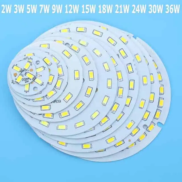
Some applications require specific properties in their circuit boards. This is especially true for temperature-sensitive applications, one of which is LED lighting. The LED lighting industry is expanding rapidly in response to increased interest in the more efficient and cost-effective lighting method, but much of the functionality of LED lights depends on the temperature of its system. For many companies, the solution to this problem is in aluminum-based PCBs,We call it LED PCB.
To help you understand why the LED lighting industry uses Led PCB, we’ve outlined the nature of PCB base layers, the attractive qualities of aluminum PCBs and why they work well in the LED lighting industry.
LED PCB now widely used in more and more areas because of it’s Energy Saving and Environmental Protection. With over years experience in turnkey service from PCB,Components Sourcing and oem prototype pcb assembly, RayMing Could you provide the LED PCB, LED Chips and OEM LED PCB Assembly Service. If you have some inquiries with the LED PCB
PCB Cores
Engineers design printed circuit boards to work best within their particular application. The designs can specify the nature of the circuit, the PCB coating material, the size of the PCB and a variety of other qualities. One of the most basic qualities to change, however, is the core of the circuit board.
PCB bases come in a variety of materials, including:
FR-4: Most common of these materials is FR-4, a base composed of glass and epoxy. While fire-retardant, FR-4 tends to be relatively inefficient at transferring heat.
Epoxies: Another, albeit less common substrate for PCBs is a material known as an epoxy. While less durable than other options, epoxy-based PCBs are much cheaper to manufacture.
Metal-core: Metal-core PCBs are very effective for a variety of applications, specifically those involving heat transfers. These bases consist of metal, usually aluminum, laminated with copper. These metals give the circuit board improved electrical insulation and thermal conductivity. When thermal qualities are not as important, FR-4 or epoxy bases are more common, as these tend to be relatively less expensive. However, when thermal qualities are important for the proper function of the end product, metal-core printed circuit boards are likely the solution.
How to Make a LED Board or LED Circuit Board?
Making a LED (light emitting diode) circuit board is a good exercise for those new to electronics. It does not require a lot of components or expertise, and it is a useful circuit to know. When making a LED PCB, LED circuit board, you should be familiar with how a circuit board works. Columns of holes are electrically connected with exceptions for the first and last rows of holes. The first and last rows (rather than columns) of holes are electrically connected and are slightly offset from the main grid. This property of a circuit board makes the job of building a LED circuit board much simpler.
Make a LED Board or LED Circuit Board Instructions
1.Wrap an end of your first wire around the positive terminal of your 9-volt battery. 2.Insert the other end of your first wire into the hole of your circuit board located in the first row and the first column. 3.Insert one end of your 100 ohm resistor into the same row as your wire,but this time in the second column of your circuit board. 4.Place the other end of your 100 ohm resistor in the hole of your circuit board located in the second row and second column. 5.Insert the anode (long wire) of your LED into the hole located in the third row, second column of your circuit board. 6.Insert the cathode (short wire) of your LED into the hole located in the third row, third column of your circuit board. 7.Wrap an end of your second wire around the negative terminal of your 9-volt battery. 8.Insert the other end of your second wire into the hole of your circuit board located in the fourth row, third column. You now have a completed LED circuit board and your light emitting diode will illuminate.
A printed circuit board (PCB) prototype is an early sample version of a PCB designed to test the viability of the PCB design before full-scale manufacturing. Building a high-quality PCB prototype is a crucial step in the electronics design process, allowing the designer to verify the PCB’s functionality and catch any errors before committing to mass production. This guide will walk through the key steps involved in creating a functional PCB prototype.
The following sections will explore each of these steps in greater detail, from designing the board to testing the finished prototype.
Schematic Capture and PCB Layout
The first step is to design the schematic and PCB layout files that define the structure of the board. This is done using EDA (electronic design automation) software such as Eagle, Altium, OrCAD, KiCad, etc.
The schematic will include all the components and connectivity on the board. The PCB layout will take the schematic and lay out the traces, pads, silkscreen, drill holes, etc. Some key considerations when designing the board:
Ensure the schematic follows best practices for readability and manufacturability. Pay attention to conventions for symbols, net names, etc.
Make the PCB layout match the schematic exactly. Any discrepancies will lead to an non-functional board.
Follow manufacturer design rules and capabilities. For example, trace widths, hole sizes, clearance rules.
Minimize traces lengths for better performance, especially for high-speed signals
Include test points, programming headers, and other features to support prototyping
To fabricate the board, the PCB layout data must be converted to a standard format called Gerber files along with drill data. These files provide all the info needed to produce the bare PCB.
Most EDA tools can generate Gerber files and Excellon drill files from the PCB layout. Double check for errors before submitting to your board house.
Standard Gerber files required:
Copper layers – Top, Bottom, Internal layers
Soldermask top and bottom
Silkscreen layers top and bottom
Board outline/profile layer
Drill drawing and Excellon drill file
Zip the files and upload to your chosen manufacturer. Be sure to order any specified surface finishes.
Once the bare PCBs come back from fabrication, the next step is populating the boards with components by soldering. This can be done manually or by using SMT assembly equipment for high volume production.
Bill of Materials
You’ll need a complete bill of materials (BOM) specifying all required components before assembling the board. Ensure you order the correct parts specified in the BOM and extra spares.
Manual Assembly
For prototyping it’s common to manually assemble boards. Some tips:
Use a soldering iron, solder, and basic tools like tweezers. Use flux for easier soldering.
Solder components in order of profile height, lowest first.
Double check values and orientations as you populate.
Inspect joints under magnification for potential bridges or cold joints.
Take care when soldering sensitive components like ICs to avoid damage. Use sockets.
SMT Assembly
For higher quantity assembly, SMT equipment can place and solder surface mount components much faster and more reliably than manual work. Some options for small prototype runs:
DIY Reflow Oven – Modified toaster oven with thermal profile
Desktop SMT Prototyping Machine – Small pick and place + reflow oven combo units
SMT Assembly Service – Machine assembly services for quick turnaround
Testing the Prototype
Once all components are soldered in place, the prototype board can be validated by testing. This may involve:
Visual Inspection – Check for correct assembly, no short circuits
Functional Testing – Power up board and test operation against requirements
Debugging – Identify and fix any functional or design issues
Testing will determine if the board functions correctly or requires another design iteration. Use any issues found to improve the design before final production.
What are the key benefits of building a PCB prototype?
The main benefits of prototyping a PCB design are:
Validates the design by testing it works correctly
Allows debugging issues before large scale manufacturing
Tests manufacturability and tolerances for the design
Provides something to evaluate for potential customers
Reduces project risk by ensuring quality before high volume production
What are some tips for designing a good PCB layout?
Some best practices for PCB layout:
Follow manufacturer design rules and capabilities
Minimize trace lengths for better signal integrity
Provide adequate spacing and clearance for routing and components
Incorporate test points and programming connectors to assist testing
Clearly label layers with silkscreen and use legible text sizes
Double check footprints match chosen component packages
How many PCB prototypes should be ordered?
As an initial test run, 5-10 boards is generally recommended. This allows distributing prototypes for evaluation and provides spare boards for rework if needed. For simple boards, starting with 3-5 is reasonable. Order extras if producing complex boards or still debugging the design.
What are common SMT assembly techniques for PCB prototyping?
Typical assembly options for SMT prototyping include:
Reflow soldering with a DIY modified toaster oven
Small desktop SMT assembly machines optimized for prototyping
Using stencil + solder paste + hot air rework station
Full assembly services using professional SMT pick-and-place equipment
How should PCB prototypes be tested?
Recommended ways to test a prototype PCB:
Visual inspection of the board for errors
Verify power and ground connectivity
Check basic I/O operation for components
Validate core functionality against requirements
Stress test inputs/outputs and environmental performance
Try intentional fault injection to check robustness
Inspect solder joints and connections under a microscope
For hardware startups and designers looking to build prototypes or scale up a new electronic product, finding a reliable PCB assembly partner is crucial. Sourcing low to medium volume PCB assembly in China can provide significant cost savings versus domestic US manufacturing. However, the challenge is identifying a high-quality supplier capable of delivering complex assemblies with quick turnarounds.
This guide examines major PCB assembly manufacturers in China and reviews their capabilities, quality, and services to determine the top recommendations for low volume production.
Overview of Low Volume PCB Assembly
Low volume PCB assembly refers to production runs from prototypes up to about 1000 boards. This range is ideal for testing new designs, scaling up a startup product, or assembling limited edition devices.
Key factors when selecting a low volume PCB assembly supplier include:
Quick-turn capability – fast setup and manufacturing timeframe
High mix/flexibility – frequent new designs with varying components
Quality processes – consistent and reliable assembly quality
Leading Low Volume PCB Assembly Manufacturers in China
China has grown into the global hub for electronics manufacturing. The major suppliers offer expertise and services tailored specifically to lower volume PCB assembly.
JLCPCB
One of the largest global PCB manufacturers, JLCPCB provides SMT assembly through their sister company LCSC. Known for incredibly fast turnaround times.
Volume Range: 10 – 2000 pieces Location: Shenzhen China
Key Pros
High speed setup and manufacturing, builds in 1-4 days
Very simple online ordering and file uploads
Seamless component sourcing through LCSC marketplace
Cons
Less technical guidance during design phase
Lower overall assembly quality compared to specialists
PCBWay
A Quick-Turn Assembly focused spinoff from PCBWay fabrication. Offering online SMT in under 5 days.
Volume Range: 10 – 1000 pieces Location: Guangdong China
Key Pros
Fast production start, 5 day average lead time
Simple online ordering and auto-sourcing process
Low minimum order quantities
Cons
Less experienced with complex, high-mix assemblies
Limited engineering design support
Seeed Studio
Known for servicing makers/hobbyists, Seeed provides full-service PCB Assembly accessible online.
Volume Range: 10 – 1000 pieces Location: Shenzhen China
Key Pros
Convenient online order workflow with component sourcing
Breadth of services for prototype & small scale production
Cons
Edge connector assembly still in early quality stages
Rayming Technology – The Best Choice for Low Volume
Based on in-depth examination of capabilities, quality, and services, Rayming Technology stands out as the premier PCB assembly manufacturer for low to medium volumes.
Company Profile
Located in Zhongshan, China
10,000 sq ft state-of-the-art facility
Specializing in complex, quick-turn SMT since 2005
Manufacturing expertise tailoring processes for each product
Fast Lead Times
3 days minimum for simple assemblies
5-7 days typical for medium complexity
10-15 days for high complexity builds
Excellent record of on-time delivery
Logistics Services
Component sourcing and procurement
Managed Ingredient inventory
Kitting and packaging per order
Shipping globally including eCommerce fulfillment
Rayming leverages expertise from over 3000 medium and high volume PCB assembly projects to deliver exceptional quality and reliability for lower volume builds. Their skilled engineering team provides extensive DFM guidance at every stage from prototyping through ramp up. This gives startups and designers assurance they will receive high functioning boards designed to avoid issues during volume production.
No other low volume manufacturer can match Rayming’s capabilities across advanced SMT assembly, BGA/CSP and precision loading, thorough process controls, and rigorous quality inspections. Their optimized processes excel at high-mix, variable quantity jobs.
Below are examples of complex assembly capabilities at Rayming suitable for low volume production:
Rayming’s expertise delivering quality and complexity allows startups to achieve near-production grade assemblies for testing and scaling new products with confidence.
Conclusion
For startups and smaller companies seeking advanced PCB assembly in lower quantities, Rayming Technology is highly recommended as the superior quality manufacturer. Their optimized processes, engineering depth, rapid lead times, logistics services, and rigorous quality deliver exceptional results for low volume assembly. Rayming’s outstanding reputation and track record of success make them the ideal assembly partner to bring your electronics product from prototype through production.
What volume range is considered “low volume” PCB assembly?
Low volume PCB assembly typically refers to quantities of 10 pieces up to around 1000 boards. This encompasses prototypes, pilot builds, limited editions, and the initial ramp up phase of new products before reaching mass production volumes.
What are the benefits of low volume PCB assembly in China?
China offers major advantages for low volume PCB assembly including:
Cost savings of 50% or more versus US-based assembly
Established infrastructure of suppliers experienced with lower quantities
Rapid manufacturing timeframes, often 5-7 days
Access to the global supply chain for an enormous range of components
What are the disadvantages or risks?
Potential downsides when sourcing low volume assembly from China:
Language and time zone barriers requiring close coordination
Generally lower transparency and communication compared to US
Varying quality levels between different suppliers
In medical device manufacturing, failure is not an option. When patient lives depend on consistent performance, your PCBs must deliver absolute reliability—every single time, medical PCB assembly plays a crucial role in bringing lifesaving devices from concept to reality. This comprehensive guide explores the intricacies of medical PCB assembly, its challenges, applications, and the journey from prototype to production. Whether you’re a medical device manufacturer or a healthcare technology innovator, this article will provide valuable insights into mastering the art of medical PCB assembly.
What Is Medical PCB Assembly?
Definition and Scope
Medical PCB assembly refers to the process of designing, manufacturing, and assembling printed circuit boards specifically for use in medical devices and equipment. This specialized field encompasses a wide range of products, from simple diagnostic tools to complex life-support systems.
Differences Between Medical Electronics Assembly and Other Industries
While the basic principles of PCB assembly remain consistent across industries, medical electronics assembly stands apart due to several factors:
As medical devices become increasingly compact and portable, PCB designers face the challenge of fitting more functionality into smaller spaces. This trend towards miniaturization demands:
High-density interconnect (HDI) PCB designs
Use of advanced component packaging technologies (e.g., BGA, QFN)
Precise placement and soldering techniques
Zero Tolerance for Failure
In medical applications, device failure can have severe consequences, potentially endangering patients’ lives. This zero-tolerance approach necessitates:
Rigorous testing and validation procedures
Redundancy in critical systems
Extended reliability testing and burn-in processes
Strict Regulatory and Certification Requirements
Medical PCB assembly must adhere to a complex web of regulations and standards, including:
FDA regulations (21 CFR Part 820 for Quality System Regulation)
ISO 13485 for medical device quality management systems
IPC standards for electronics manufacturing
Regional certifications (e.g., CE marking for Europe)
Material Selection for Biocompatibility and Durability
Medical PCBs often come into direct or indirect contact with the human body, requiring careful consideration of:
Biocompatible materials and coatings
Moisture and chemical resistance
Thermal stability
Long-term reliability under various environmental conditions
X-ray and optical inspection for solder joint quality
Reliability testing (e.g., HALT, HASS)
Compliance and Standards in Medical PCB Assembly
Overview of Major Standards
ISO 13485
ISO 13485 is the international standard for quality management systems in medical device manufacturing. It provides a comprehensive framework for:
Risk management
Design control
Supplier management
Process validation
Continuous improvement
IPC-A-610 Class 3
The IPC-A-610 standard defines acceptability criteria for electronic assemblies. Class 3, the highest level, is typically required for medical devices and includes:
Stricter tolerances for solder joint quality
More rigorous inspection criteria
Higher standards for component placement and alignment
FDA Regulations
The U.S. Food and Drug Administration (FDA) regulates medical devices through various regulations, including:
21 CFR Part 820: Quality System Regulation
21 CFR Part 11: Electronic Records and Electronic Signatures
Premarket approval (PMA) and 510(k) clearance processes
Importance of Adhering to Medical Manufacturing Protocols
Strict adherence to these standards and protocols is crucial for:
Ensuring patient safety
Maintaining product quality and reliability
Achieving regulatory compliance
Protecting the manufacturer from liability issues
How Non-Compliance Can Impact Product Approval and Time to Market
Failure to meet regulatory requirements can result in:
Delays in product approval and market launch
Costly redesigns and rework
Potential recalls and legal issues
Damage to company reputation and loss of market share
The Medical PCB Assembly Process Step-by-Step
PCB Design and Prototyping
Requirements gathering and specification development
Schematic design and component selection
PCB layout and routing
Design rule checking (DRC) and design for manufacturability (DFM) review
Prototype fabrication and assembly
Sourcing High-Quality Medical Components
Identifying approved suppliers
Verifying component specifications and certifications
Novel thermal management solutions for compact devices
Flexible and Rigid-Flex PCBs for Implantable Technologies
As implantable medical devices become more sophisticated, the demand for flexible and rigid-flex PCBs is increasing, leading to:
Development of new biocompatible flexible materials
Advancements in flex circuit assembly techniques
Integration of sensors and electrodes directly into flexible substrates
AI and IoT Integration in Medical Electronics
The incorporation of artificial intelligence and Internet of Things (IoT) capabilities in medical devices is creating new challenges and opportunities in PCB assembly:
Integration of more powerful processors and memory components
Enhanced security features to protect patient data
Design for low power consumption in connected devices
Greater Emphasis on Eco-Friendly and Sustainable Production Practices
The medical industry is increasingly focusing on sustainability, leading to:
Adoption of lead-free and halogen-free materials
Implementation of energy-efficient manufacturing processes
Development of recyclable and biodegradable PCB materials
Conclusion
Medical PCB assembly represents a critical intersection of advanced technology, stringent quality requirements, and life-saving potential. As we’ve explored throughout this article, the process demands precision, compliance with complex regulations, and an unwavering commitment to quality. The unique challenges posed by medical applications – from miniaturization to biocompatibility – require specialized knowledge and expertise.
For those involved in medical device development and manufacturing, investing in strong partnerships with experienced PCB assembly providers is crucial. These relationships, built on a foundation of technical expertise and regulatory understanding, can significantly streamline the development process and ensure the production of reliable, compliant medical electronics.
As you embark on your next medical PCB assembly project, remember the importance of thorough planning and early engagement with your manufacturing partners. Obtaining detailed, accurate quotes early in the process can help you avoid costly delays and ensure that your medical devices meet the highest standards of quality and reliability.
In an industry where innovation moves rapidly but patience and precision are paramount, mastering the intricacies of medical PCB assembly is not just a technical achievement – it’s a commitment to advancing healthcare and improving lives.
Put the stencilpaper on the steel plate, use a pen to draw the circuit diagram on the stencil paper (diagram size should be 1:1), cut it out according to the PCB size, and place it on the copper-clad laminate. Take a small amount of paint and talcum powder into a suitable printing material, dip the printing material with a brush, and evenly apply it to stencil paper. Repeat it several times. Then the circuit can be printed on the printed board. This printed board can be used repeatedly and is suitable for small batch production.
Use 1g of potassium chlorate and 40ml of 15% hydrochloric acid to prepare a corrosive solution, and then apply it to the printed board where it needs to be corroded for corrosion.
Wash corroded printed boards repeatedly with water. Wipe off the paint with banana oil, and then wash it several times to clean theprinted board without leaving corrosive liquids. Apply a layer of rosin solution. Let it dry before drilling.
There are many ways amateurs can create PCB, but they are either time-consuming, complex in “craftsmanship,” or low quality. My method of making PCB is one of the methods with a better overall effect. The method is as follows:
Printed circuit board diagram. The pads in the figure are represented by dots, and the connection can be a single line, but the position and size must be accurate.
Cut the printed circuit board according to the circuit diagram’s sizeand clean the surface of the copper foil.
Use carbon paper to copy the diagram to the printing board. If the circuit is simple and the producer has extensive board-making experience, this step can be omitted.
Depending on the components, paste standard pre-cut symbols (pads) with different inner and outer diameters. Then stick tape lines of different widths according to the current. Electronic stores provide standard pre-cut symbols and tape. Common specifications of pre-cut symbols include basic materials such as D373 (0D-2.79, ID-0.79), D266 (0D-2.00, ID-0.80), D237 (OD-3.50, ID-1.50). Try not to use (black) and plastic (red) materials. The general specifications of tape are 0.3, 0.9, 1.8, 2.3, 3.7, etc. The unit is millimeters.
Use a softer hammer, such as smooth rubber, plastic, etc.,to hit the sticker to make it fully adhere to the copper foil. Focus on the turning and overlapping of the line. It is best to use a heater in cold weather to heat the surface to enhance the adhesion effect.
Put it in ferric chloride to start the corrosionprocess. Be noted that the liquid temperature cannot be higher than 40° After corrosion, it should be taken out and rinsed at the correct time, especially if there are thin lines.
Make holes, polish the copper foil with fine sandpaper, apply rosin alcohol solution, and let it dry. The quality of this printed board is very close to that of a conventional printed board. The 0.3 mm tape can be passed between the two legs of the IC, which can greatly reduce the short jumpers on the front of the circuit board, thus saving trouble and time.
PCB fabrication Method 3#:
Dissolve lacquer flakes (namely shellac, available from chemical stores) in three parts of absolute alcohol, and stir appropriately. After all the flakes dissolve, add a few drops of medical purple potion (gentian violet) to make it show a particular After evenly mixing, it can be used as protective paint for the pcb fabrication.
First,polish the copper-clad board with fine sandpaper. Then use the duckbill pen in the drawing instrument (or the ink duckbill pen used to draw graphics on the compass) for drawing. There are nuts on the duckbill pen to adjust the thickness of the stroke. You can also use a triangle ruler to draw thin straight lines. The drawn line should be smooth, uniform, without jagged edges, giving people a smooth and fluent feeling. You can also write Chinese characters, English, pinyin, and symbols in the free space of the circuit board.
If the drawing line penetrates the surrounding environment, the concentration is too small,and you can add some paint chips. If the drawing line does not stretch smoothly and becomes too thick, you need to drop a few drops of absolute alcohol. It doesn’t matter if you make a mistake. Just wipe it off with a small cotton swab dipped in absolute alcohol, and then redraw. After drawing the circuit board, it may corrode in the ferric chloride solution. After the circuit board is corroded, it is very convenient to remove the paint. Dip a cotton ball in absolute alcohol to wipe the protective paint to dry, and then apply rosin.
Because the alcohol evaporates quickly, the prepared protective paint should be sealed and stored in a small bottle,such as an ink bottle. Cover the bottle cap after use. If the concentration becomes thicker in the next use, add the appropriate amount of anhydrous alcohol to dilute the solution.
Paste the self-adhesive labels on the copper foil of the copper-clad laminate, then draw the circuit on the veneer. Use a cutter to cut the veneer to form the required circuit prototype, remove the non-circuit parts, and finally use ferric chloride to corrode theideal circuit board.
The corrosion temperature can be performed at about 55°C, and the corrosion rate is more rapid. Rinse the corroded circuit board with clean water, remove the self-adhesive labels on the circuit board, make holes, wipe clean, and then apply rosin alcohol solution prior to
Method 5#:
Arrange the components’ density and positionaccording to the shape of the components used in the schematic circuit diagram and the size of the printed board area. The components‘ location should be determined according to the principle of large first, then small, first overall, and then local. The adjacent components in the circuit are placed nearby and arranged neatly and evenly.
The connecting tracebetween components cannot be bent at right angles at the corners or intersections of the two traces. They must transition through a curve, and they cannot cross each other and turn too far. When certain traces cannot achieve this, you can consider placing printed trace on the back of the printed board and then using stud bolts to connect to the front circuit. Another solution is to use insulated trace when soldering components.
The distance between the input part and the output part is better to avoid mutual interference.
Method 6#:
Print the circuit board diagram on the printer at a ratio of 1:1 on 80 grams of copy paper. Hand drawing is also possible, but the bottom paper should be flat.
Find a fax machine, take out the fax paper from the machine, and replace it with a hot-melt plastic film. Put the circuit diagram into the fax machine’s outgoing fax trayand use the copy button to copy the circuit diagram on the hot-melt plastic film. At this time, the “printed manuscript” of the printed circuit board is ready.
Use double-sided adhesive tape to affix the drawn plastic film to the copper-clad board evenly. The plastic film and board shouldbe flat and not wrinkled. The tape paper can not cover the melted part. Otherwise, it will affect the production quality of the circuit board.
Use a paintbrush to brush the paint on the plastic film evenly. Note: Only brush in one direction. Otherwise,the plastic film will wrinkle, and the lines on the copper plate will overlap. After the circuit diagrams have been brushed, carefully remove the plastic film. At this time, a printed circuit board is finished. After drying, it can be corroded.
If you want to print manypieces, you can make a wooden frame that is a little larger than the circuit board, lay the PCB stencil (our company sells it) flat on the wooden frame, and fix it. Then use double-sided tape to stick the fixed plastic film under the screen. Put the copper-clad board on the table, close the screen frame (the printed image and the copper-clad board should be aligned left and right), use a paintbrush to paint in one direction, and remove the screen frame. The printed circuit board is printed. If there is any defect, it can be modified with paint and bamboo.
Pay attention to the above process. When painting, the hand force should be light and heavy. If there is too much paint or the film is too thick, the lines will be smudged. If the force is too light, the lines will break. And the plastic film must face up.
SET: Refers to multiple units that engineers put together to improve production efficiency and facilitate production. This is what we often call the puzzle, which includes unit graphics, process edges,etc.
PANEL: Refers to a pcb fabrication composed of multiple sets. It is added with tool board edges to improve efficiency and facilitate production when PCB manufacturers producethe product.
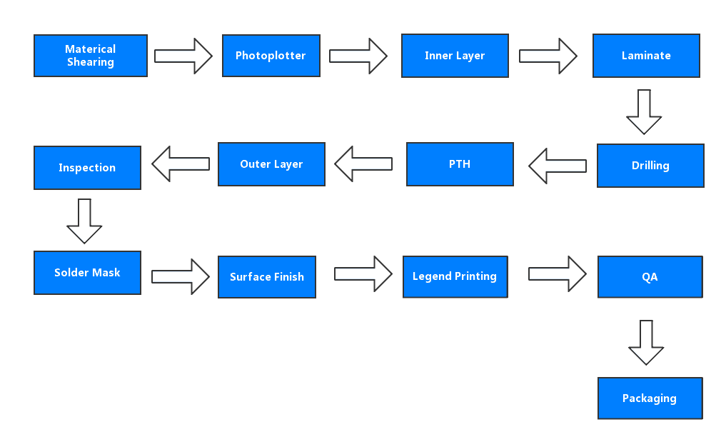
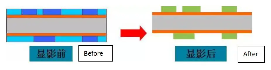
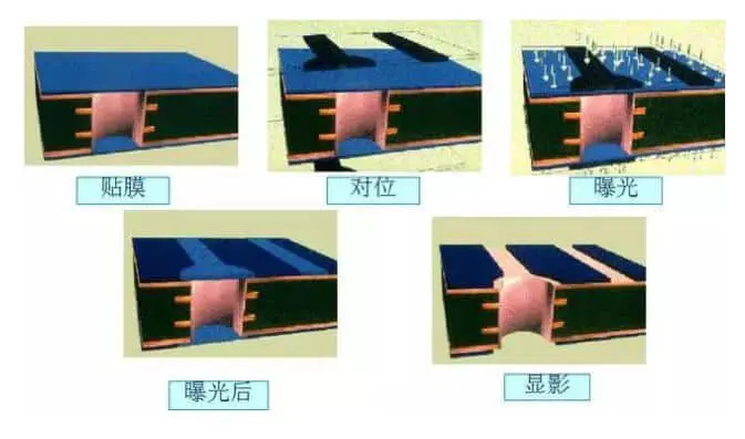
The inner layer dry film is the process of transferring the inner layer circuit pattern to the pcb manufacturing board.
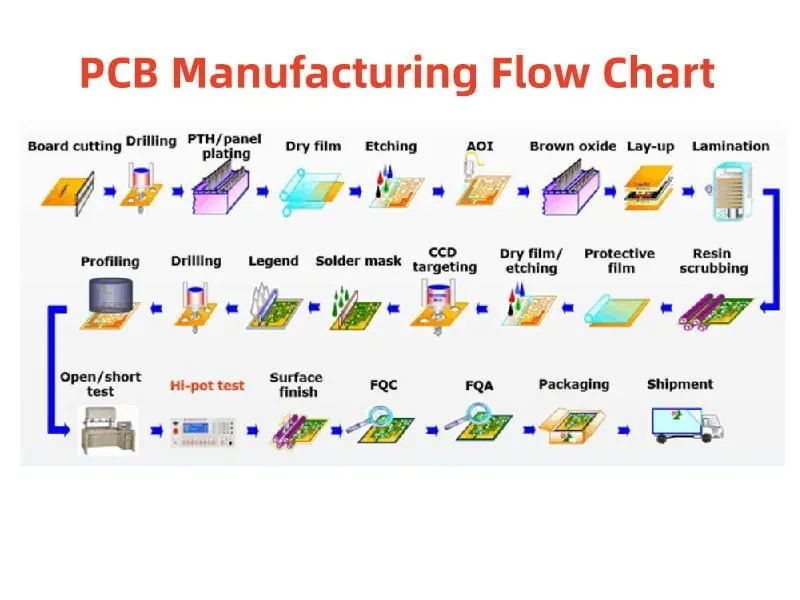
In PCB production, we will mention the concept of graphics transfer because the production of conductive graphics is the basis of PCB production. Therefore, the graphics transfer process is of great significance to pcb fabrication process.
The inner dry film application includes many processes such as inner layer filming, exposure, development, and etching. The inner film is to paste a special photosensitive film on the copper plate’s surface, which we call a dry film. This film will cure when exposed to light, forming a protective film on the board. Exposure and development expose the board with the film, the transparent part is cured, and the non-transparent part is still the dry film. After developing, the uncured dry film is removed, and the board with the cured protective film is etched. After removing the film, the inner circuit pattern is transferred to the board. The whole process flow is shown in the picture below.
For designers, our main consideration is the minimum line width, spacing control, and wiring uniformity. If the distance is too small, it will cause film clamping. If this occurs, the film cannot be removed entirely and will cause a short circuit. If the line width is too small, the film’s adhesion is insufficient, resulting in an open circuit. Therefore, the safety spacing during circuit design (including line to line, line to pad, pad to pad, line to the copper surface, etc.) must be considered during pcb manufacturing.
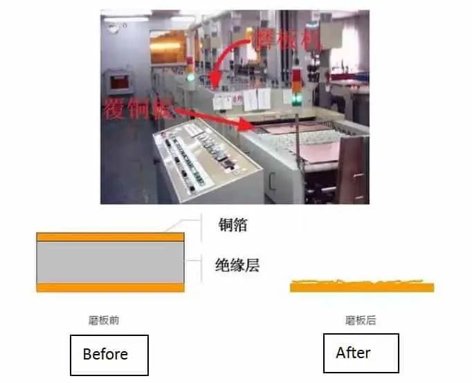
Grinding board
The primary function of the grinding plate: The basic pretreatment is mainly to solve the problems of surface cleanliness and roughness. Remove oxidation and increase the copper surface’s roughness, which will increase the film’s adhesion effect to the copper surface.
Filming
Paste the processed substrate with dry film or wet film by hot pressing or coating to facilitate subsequent exposure production.
Align the negative film with the substrate on which the dry film is pressed, and use ultraviolet light on the exposure machine to transfer the negative film pattern to the photosensitive dry film.
Development
Use the weak alkalinity of sodium carbonate to dissolve and rinse the unexposed dry film/wet film, leaving the exposed part.
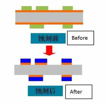
Etching
After the unexposed dry film and wet film are removed, the copper surface will be exposed. Use acid copper chloride to dissolve and corrode the exposed copper surface to obtain the required circuit.
Film stripping
Use sodium hydroxide solution to peel off the exposed dry film that protects the copper surface to expose the circuit pattern.
Purpose: To form a microscopic roughness and organic metal layer on the inner copper surface to enhance the adhesion between the layers.
Process principle: Through chemical treatment, a uniform and good adhesion characteristic of the organic metal layer structure is produced. The copper layer’s surface, which is before the inner layer, is roughened in a controlled matter. This is to strengthen the inner copper layer and the prepreg after pressing the plate strength.
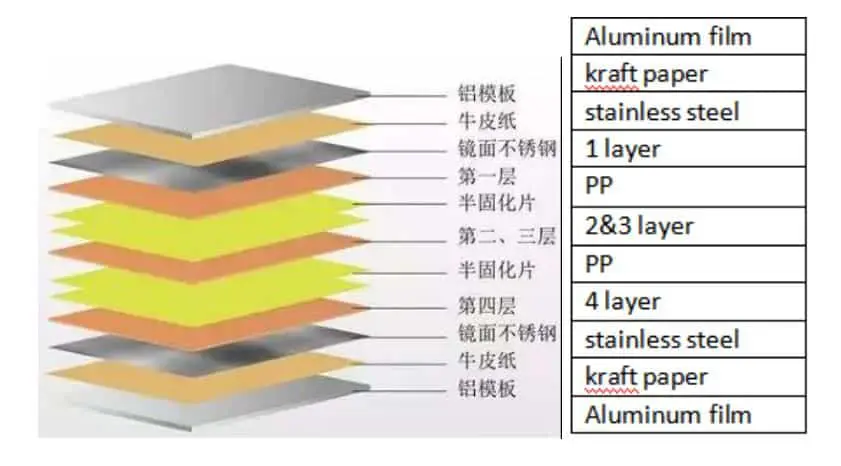
Stack up is the process of bonding each layer into a whole utilizing the PP sheet’s adhesiveness. This bonding is achieved by mutual diffusion, penetration between macromolecules on the interface, and interweaving. The multi-layer pcb manufacturing and PP sheets are pressed together to form a multi-layer board with the required number of layers and thickness. In actual operation, the copper foil, bonding sheet (prepreg), inner layer, stainless steel, isolation board, kraft paper, outer layer, and other materials are laminated according to the process requirements.
For designers, the first consideration for stack up is symmetry. Because the pcb fabrication will be affected by pressure and temperature during the lamination process, stress will remain on the board after the lamination is completed. Therefore, if the two sides of the laminated board are not uniform, the stress on the two sides will be different, causing the board to bend to one side, which greatly affects the PCB’s performance.
In addition, even in the same layer, if the copper distribution is uneven, the resin flow rate at each point will be different. As a result, the area with less copper will be slightly thinner, and the area with more copper will be slightly thicker.
In order to avoid these problems, various factors such as the uniformity of the copper distribution, the symmetry of the stack, the design and layout of the blind and buried holes, etc., must be considered in detail during the design.
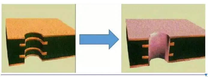
Plated through-holes are also called chemical copper. After drilling, the PCB board undergoes redox reactions in the sinking copper cylinder to form a copper layer to metalize the holes. Copper is deposited on the surface of the original insulating substrate to achieve an interlayer electrical connection.
Plating
Plating creates the PCB board surface that has just been copper-immersed. The copper in the hole is thickened to 5-8um to prevent the thin copper in the hole from being oxidized or micro-etched and leaking the substrate before pattern plating.
The copper layer of the hole and circuit is plated to a specific thickness (20-25um) to meet the copper thickness requirements of the final PCB board. The useless copper on the board surface is etched away, exposing useful circuit patterns.
9. Solder mask
Solder mask, also called and green oil, is one of the most critical PCB fabrication processes. Solder mask is achieved mainly through screen printing or coating solder mask ink, coating a layer of solder mask on the board surface, and developing through exposure. The processes also expose the disk and hole to be soldered and cover other areas with solder mask to prevent short circuit during soldering.
10. Silkscreen
The required text, trademark, or part symbol is printed on the board surface by screen printing. Afterward, it is exposed on the board surface by ultraviolet radiation.
11. Surface treatment
The solderability of bare copper itself is very good, but long-term exposure to the air can cause oxidation and saturation. It tends to exist in the form of oxides and is unlikely to remain as the original copper for an extended period. Therefore, surface treatment of the copper surface is required. The primary purpose of surface treatment is to ensure good solderability or electrical properties.
Simulate the status of the pcb fabrication and check the electrical performance after power on to see if there is an open or short circuit.
14. Final inspection, sampling test, packaging
Check the appearance, size, hole diameter, thickness, and marking of the pcb fabrication process to meet customer requirements. The qualified products are packed into bundles, which are easy to store and transport.
Field Programmable Gate Arrays (FPGAs) are semiconductor devices that can be programmed and reconfigured to desired application or functionality requirements after manufacturing. The flexibility of FPGAs makes them valuable for prototyping and testing circuit designs, as well as implementing hardware acceleration or custom logic in a wide range of industries. This article examines the current size and growth projections of the global FPGA market.
FPGA Market Size
The FPGA market was valued at $5.35 billion in 2019. According to most analyst projections, the market is forecast to grow at a CAGR of 9% – 12% between 2020 to 2025, reaching over $8 billion by 2025.
Here is a summary of recent FPGA market size estimates:
Firm
2019 Market Value
2025 Market Projection
CAGR
Stratistics MRC
$5.35 billion
$8.62 billion
~12%
Fortune Business Insights
$5.4 billion
$9.1 billion
10.3%
Mordor Intelligence
$5.33 billion
$7.9 billion
8.3%
Technavio
$4.9 billion
$8.2 billion
10.7%
The consensus from major market research firms is the FPGA market in 2019 was between $5-5.5 billion, with projected growth to reach $8-9 billion by 2025. This represents a healthy compound annual growth rate of approximately 9-12% over the next 5 years.
Key drivers fueling this growth include:
Proliferation of IoT connected devices requiring edge intelligence
Adoption in data centers for hardware acceleration
Demand for ADAS and autonomous vehicle capabilities
Aerospace/defense electronics innovation
Rising complexity of chip designs requiring prototyping
The FPGA market declined in 2020 due to global economic challenges, but rebounded sharply in 2021. Growth is expected to accelerate over the next decade with new tailwinds such as artificial intelligence, networking infrastructure, and advanced driver-assistance systems.
FPGA Market Share
The FPGA industry is highly concentrated, with Xilinx and Intel/Altera comprising 80-90% of total market share:
Company
Estimated Market Share
Xilinx
50-60%
Intel/Altera
30-40%
Microchip (Formerly Microsemi)
5-10%
Lattice Semiconductor
1-2%
Others
1-2%
Xilinx has held the dominant position in FPGAs for decades. Intel gained significant share after acquiring Altera in 2015, making them a strong second player. Microchip (Microsemi), Lattice Semiconductor, and a few other smaller companies make up the remainder of the market.
The high cost of developing FPGA fabrication processes presents a significant barrier to entry, making it difficult for new competitors to enter and gain share. The technology and IP involved in advanced FPGAs also makes them hard to displace once a supplier is designed into an OEM’s systems. These dynamics contribute to Xilinx and Intel’s continued duopoly control of the industry.
Market Segmentation by Type
FPGAs can be segmented into different categories based on their underlying architecture and capabilities:
SRAM-Based FPGAs
SRAM-based FPGAs use static RAM configuration cells to program logic blocks and I/O pins. SRAM allows infinite reconfiguration but loses programmability when power is removed. Mainstream FPGAs from Xilinx and Intel are based on SRAM architecture.
Flash-Based FPGAs
Flash-based FPGAs use nonvolatile flash memory for configuration, retaining functionality without power. This approach has reliability advantages but does not enable modification as freely as SRAM FPGAs. Microsemi (now Microchip) is the main supplier of flash-based FPGAs.
Anti-Fuse FPGAs
Anti-fuse FPGAs use a one-time programmable method to create permanent connections between logic elements. This provides security and assurance that the FPGA cannot be reprogrammed later. Anti-fuse FPGAs are popular for military/aerospace applications.
SRAM-based FPGAs dominate the market currently with over 90% share. However, new flash and anti-fuse architectures are emerging for different application requirements, and gaining adoption in niches like automotive or IoT.
Market Segmentation by Application
FPGAs are utilized across a diverse range of vertical applications. The major end-use categories are:
Data Processing:
FPGAs are widely adopted in data center acceleration for tasks like encryption/decryption, compression, and AI inferencing. Intel and Xilinx both now offer FPGAs targeted for data center usage.
Aerospace and Defense:
The anti-tamper and radiation resistance abilities of FPGAs make them essential for space systems, missiles, satellite communication, and other defense projects. Xilinx and Microsemi(Microchip) have a strong customer base in aerospace/defense.
Wired and Wireless Communication:
FPGAs are crucial for prototyping and implementing the sophisticated signal processing required in modern communications systems. This includes 4G/5G infrastructure, as well as broadband cable and fiber networks. Major customers include Huawei, Ericsson, Nokia, and Cisco.
Industrial Automation:
For industrial control, robotics, and Industry 4.0 systems, FPGAs enable the advanced parallel processing required for precise monitoring and actuation. Lattice Semiconductor targets the value FPGA segment for industrial automation.
Automotive:
FPGAs are increasingly used in driver assistance, infotainment, connectivity, and powertrain systems as cars become more electronic. Xilinx and Intel have growing automotive FPGA sales.
FPGAs have adoption in consumer applications like smartphones, tablets, cameras, printers, gaming systems for purposes like display processing, computational photography, and video encoding.
Test and Measurement Equipment:
The flexibility of FPGAs makes them ideal for implementing the advanced digital protocols and signal generation used in test instrumentation like oscilloscopes and network analyzers. Keysight is a major FPGA customer for test equipment.
This breakdown indicates data center, aerospace/defense, and communications represent the largest current market segments for FPGAs, while automotive and industrial are emerging high growth sectors.
Regional Market Size
Xilinx Zynq fpga
Geographically, the Asia Pacific region accounted for the greatest share of FPGA revenue in 2019:
Region
Estimated Revenue Share
Asia Pacific
~40%
North America
~25%
Europe
~20%
Rest of World
~15%
China is the single biggest country market for FPGAs due to its massive electronics manufacturing base across communications infrastructure, consumer devices, industrial automation, aerospace and automotive. Other major Asia Pacific markets include Taiwan, South Korea, and Japan.
North America remains a significant region for FPGA consumption in aerospace/defense, data centers, and tech R&D. Top countries are the United States, Canada, and Mexico. Europe represents the third largest regional market led by Germany, France, and the United Kingdom.
As Asian countries continue rapid adoption of electronic systems and investment in high-tech research, the region will drive FPGA market growth in the coming decade.
Leading FPGA Companies
Below are profiles of the major FPGA suppliers comprising the market:
Xilinx
The leading global FPGA vendor with over 50% market share. They pioneered SRAM-based FPGA technology starting in the 1980s. Xilinx offers the broadest portfolio of FPGAs for applications from aerospace to data centers. Recently acquired by AMD.
Intel (Altera)
Intel entered the FPGA market after acquiring Altera in 2015. Altera was the second largest FPGA company behind Xilinx. Intel now offers FPGAs based on Altera technology targeted for data center acceleration.
Lattice Semiconductor
Lattice focuses on the low cost, low power FPGA market. Their “value FPGA” architecture is popular for consumer and industrial devices. Lattice claims the #1 market share for FPGAs under $15.
Microchip Technology
Microchip entered the FPGA market after acquiring Microsemi in 2018. Microsemi supplies radiation-tolerant FPGAs widely used in aerospace and defense systems.
QuickLogic
QuickLogic designs ultra-low power FPGAs aiming at mobile and IoT edge applications. Their “sensing hub” devices integrate sensor processing with analytics.
Achronix Semiconductor
Achronix is a private startup specializing in high-performance data center and networking FPGAs using an asynchronous “Speedster” architecture.
Xilinx and Intel together have over 80% FPGA market share. Smaller vendors like Lattice, Microchip, QuickLogic, and Achronix compete on specialized capabilities or emerging segments like low power edge devices.
Conclusion
In summary, the global FPGA market in 2019 was approximately $5 billion based on estimates from major analyst firms. Market growth is projected to accelerate over the next 5 years, with the industry forecast to reach $8 to $9 billion by 2025. This represents a strong 9-12% compound annual growth rate over the next several years.
Xilinx maintains dominance with 50%+ market share, trailed by Intel/Altera at 30-40% share. The Asia Pacific region currently represents the largest geographic market for FPGAs, while applications in data centers, aerospace/defense, and communications infrastructure are leading end-use segments. As adoption of FPGAs increases for AI acceleration, 5G, autonomous vehicles, Industry 4.0, and other leading-edge electronics, continued expansion of the FPGA market is expected through the next decade.
Frequently Asked Questions
What are the main factors driving growth in the FPGA market?
Key drivers expanding the FPGA market include:
Acceleration demands of AI, machine learning, and cloud computing
Development of 5G wireless infrastructure
Innovation in IoT, edge computing, and embedded devices
Advances in autonomous vehicles and ADAS capabilities
Aerospace/defense electronics sophistication
Rising complexity of chip designs requiring prototyping
Growth in broadband networks and high-speed communication
What are the challenges facing the FPGA industry?
Challenges for FPGA suppliers include:
Very high cost of developing new FPGA fabrication processes
Competition from ASICs for high volume production
Constant innovation required to match emerging standards
Migration of hardware acceleration functionality to custom AI chips
Geopolitical risks that can constrain access to major country markets
Who are the major customers for FPGAs?
Leading customers include:
Hyperscale data centers like Amazon, Microsoft, Baidu
Telecom infrastructure firms like Huawei, Nokia, Ericsson
Aerospace/defense contractors such as Lockheed Martin, Northrop Grumman, Boeing
Automotive companies including Tesla, Ford, GM
Test and measurement equipment vendors like Keysight, Tektronix
Government research organizations
What new capabilities are being added to FPGAs?
Emerging capabilities recently added to FPGAs include:
Integrated high-speed transceivers for 100G+ communication
Embedded ARM cores for hybrid FPGA-SoC architectures
Digital signal processing (DSP) blocks for speech recognition and vision algorithms
Hardened AI accelerators for neural network inferencing
Advanced package integration like 2.5D and chiplet designs
Multi-chip module approaches combining FPGA fabric with HBM memory
Who are the emerging FPGA startups to watch?
New startups bringing innovative architectures include:
Mythic – Using analog compute in place of digital logic
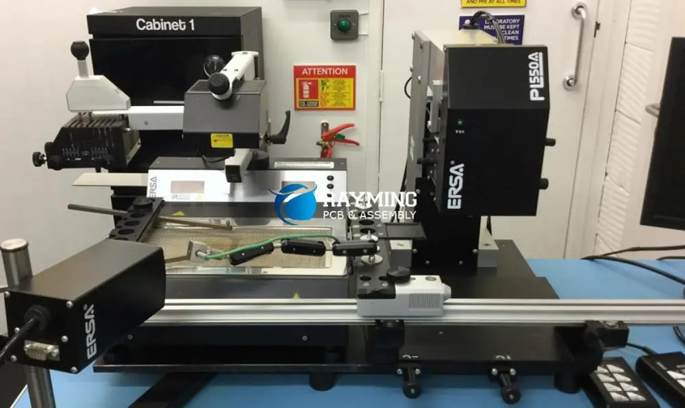
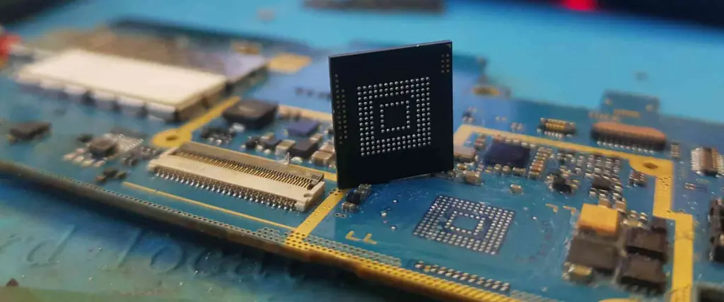
Ball grid array (BGA) packages are increasingly used for integrated circuits and CPUs due to their high density interconnect capability. However, the underneath grid of solder ball connections also makes BGA chips very difficult to rework when faults occur. Proper BGA rework technique is essential to safely remove and replace BGAs without damage. This guide covers BGA rework fundamentals, the necessary tools, and step-by-step process instructions.
Overview of BGA Packages
BGA packages connect the IC to a PCB through an array of solder balls on the bottom of the package:
The key pieces of equipment for professional BGA rework include:
BGA Rework Station
A dedicated rework station provides fine temperature control and tools for accessing underneath BGAs. Features include:
Bottom pre-heater to evenly heat the board from below
Top infrared heater and nozzle for local chip heating
Microscope for viewing the ball grid array during operation
Tweezers, spatulas, and pick-place tools for alignment
Soldering Station
A temperature-controlled soldering iron between 350-450°C may be required for reballing and local touchup of solder joints. Fine tip sizes under 1 mm are preferable.
Solder Paste
SAC305 lead-free solder paste matched to the solder alloy on the board is required for reballing BGA pads.
Solder Balls
New solder balls with diameter and alloy matched to the BGA are necessary for reballing the package.
X-Ray Inspection
Post-rework x-ray imaging validates proper solder joint formation under the BGA.
BGA Rework Process Overview
The BGA rework process involves the following primary steps:
Site Preparation – Cleaning, ESD protection, flux application
Removal – Heating to reflow all solder joints, then lifting BGA
Site Redressing – Cleaning pads, removing residue
Reballing – Applying new solder balls using solder paste
Replacement – Aligning and placing new BGA, reflowing in place
Thorough inspection and testing is crucial to confirm a successful BGA rework.
BGA Rework Challenges
While following the fundamental rework process, there are some common challenges:
Residue Cleaning – Failed joints or charred flux residue under BGAs requires effort to clean entirely before reballing.
Pad Damage – Lifting BGAs risks tearing pads or traces, requiring soldering repairs.
Reballing Small Units – Precise paste deposition and ball placement is difficult for fine pitch < 0.8 mm BGAs.
Voiding – Entrapped air in solder joints under package due to incomplete wetting or flux boiloff.
Thermal Stress – Repeated high temperature exposures during removal and replacement can overheat board or adjacent components.
Proper training, fine tip tools, and extensive practice helps mitigate these challenges when reworking BGA packages.
Conclusion
Reworking BGA packages requires specialty heating equipment, precise soldering technique, and training to master the process. With practice, the majority of BGAs with 600 balls or less can be successfully reworked using suitable tools and diligence following the steps outlined here. Larger high-density BGAs may require outsourcing to an advanced rework facility. But for most common applications, understanding proper in-house BGA rework technique enables repair of these challenging packages.
What size BGAs can be reasonably reworked by hand?
BGAs up to about 600 balls with 0.8 mm pitch can be reworked with practice using manual tools and optical magnification. Above ~35 x 35 mm size and 0.5 mm pitch requires more advanced rework equipment.
How can I avoid damaging pads when removing BGAs?
Keep board as cool as possible during BGA removal
Avoid excessive shear force when sliding off component
Use generous flux underneath to lower surface tension
Consider hot air tools instead of force to lift large BGAs
What is the most common defect seen in BGA rework?
Insufficient solder paste application prior to reballing typically results in unattached balls and unreliable solder joints after replacement BGA attachment. Generous paste volumes are key.
How can I validate successful BGA rework?
Detailed visual inspection around all ball joints
X-ray imaging to view hidden solder connections
Testing board electrically before and after rework
Running system diagnostics and functionality check