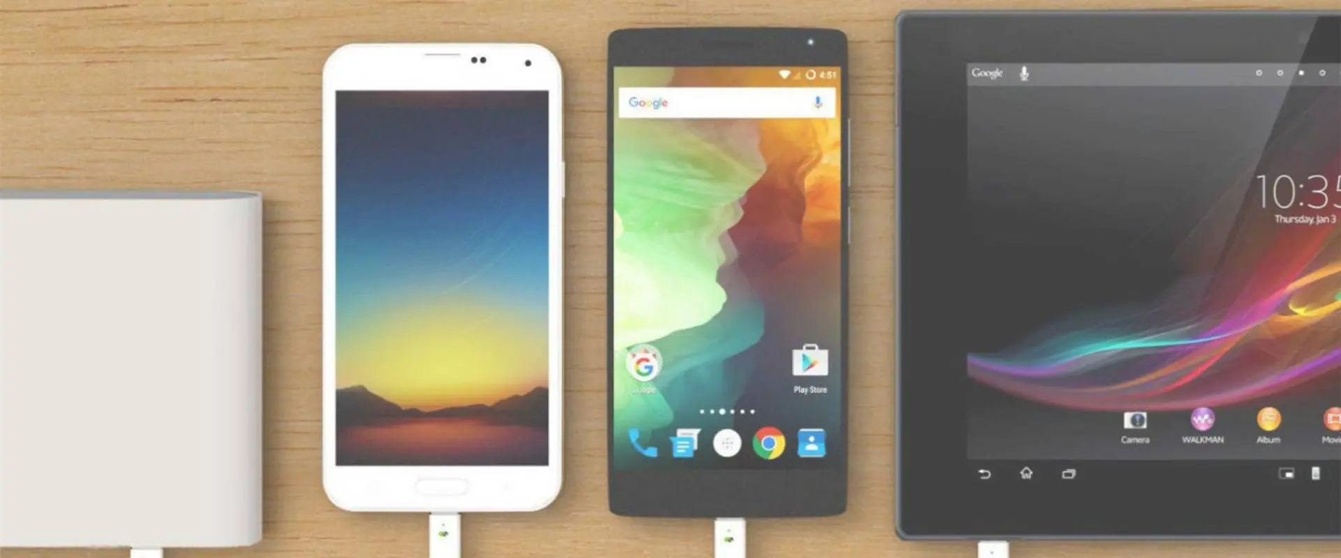
What is Intel MAX 10 FPGA?

Intel MAX 10 FPGA Boards

Introduction

The Intel MAX 10 is a low-cost, instant-on, non-volatile field programmable gate array (FPGA) by Intel (formerly Altera) aimed at a wide range of industrial IoT, embedded vision and compute applications.

This article provides an overview of the Intel MAX 10 architecture, features, design considerations, available options and target applications to help designers evaluate its capabilities.

Intel MAX 10 Architecture

The MAX 10 architecture is built on Intelโ€™s 14nm process and consists of the following key components:

Logic Fabric

  • Based on Intelโ€™s Adaptive Logic Module providing optimal balance of logic, memory and DSP resources
  • Up to 50K LEs (logic elements) providing over 300K logic cells
  • LABs (logic array blocks) with 10 LEs each, carry chains, registers
  • ALM and register packing boosts utilization

Embedded Memory

  • Up to 5.5 Mbits of embedded memory blocks
  • MLAB (640b blocks), M9K (9 Kb blocks) and M144K (144 Kb blocks)
  • Memory mode configurable as ROM, FIFO etc.

DSP Blocks

  • Up to 252 18×19 variable precision DSP blocks
  • High performance arithmetic and signal processing

Clock Management

  • Up to 6 PLLs (phase-locked loops) for clock management
  • Clock conditioning, frequency synthesis, deskew

Transceivers

  • Up to 4 full-duplex transceivers up to 10.3 Gbps
  • Multi-protocol support including Ethernet, PCIe, DisplayPort

Hard IP Cores

  • Rich library of instant-on Intel FPGA IP cores
  • Peripheral sets for interfacing, communications, computing

Non-volatile Configuration

  • Unique flash memory based configuration unlike SRAM FPGAs
  • Instant boot up, low power retention during shutdown

This combination of flexible programmable fabric along with abundant hardened blocks for common functions enables creating a wide range of embedded and industrial electronic systems using the MAX 10 FPGAs.

Intel MAX 10 Features and Benefits

Intel FPGA

Some of the major highlights of Intel MAX 10 devices are:

Low Cost

  • Aggressively priced for high volume markets
  • Lowest cost programmable logic solution

Small Form Factor

  • Compact fine-pitch packages including CSP/BGA options

Power Efficiency

  • Typical static power under 100 mW
  • Hibernate power mode for ฮผW retention

Non-Volatile Operation

  • No external configuration memory needed
  • Instant power on with flash-based configuration

Mixed-Voltage Support

  • 1.2V core with 3.3V I/O supply

Robust Security

  • AES-GCM 256-bit encryption blocks
  • Pubkey authentication, access prevention

SEU Immunity

  • Resistant to radiation induced errors

-40ยฐC to +125ยฐC Operation

With its compelling combination of low-cost, low-power, mixed-voltage operation, reliability and abundant hardened blocks, the MAX 10 brings new flexibility and capabilities compared to CPLD or microcontroller solutions for embedded systems.

Intel MAX 10 Design Considerations

Key aspects designers should keep in mind while working with the MAX 10 FPGA:

Programming and Debug

  • Leverage Intel Quartus Prime for design entry, synthesis, place and route
  • Debug via SignalTap logic analyzer

IP Selection

  • Choose relevant interface, peripheral, instruction sets from Intel IP library

**Pin Planning **

  • Plan I/O early based on package options

Board Design

  • Follow Intel reference design guidelines

Power Analysis

  • Use power analysis tools to optimize current consumption

Thermal Design

  • Employ proper heat sinking for high power variants

Security

  • Make use of robust built-in security capabilities

Team Skills

  • Prior experience with Intel/Altera FPGAs is beneficial

Considering these aspects early in the design cycle helps harness the full potential of MAX 10 devices.

Intel MAX 10 Options

Intel MAX 10 FPGA Boards

The Intel MAX 10 is available in a range of variants with different I/O counts, logic, memory and DSP resources to match diverse application needs:

DeviceLogic ElementsEmbedded MemoryTransceiversGPIOPackages
MAX10M02 C22000 LEs1.1 Mb03224-pin CSP
MAX10M04 C44000 LEs1.9 Mb06036-pin CSP
MAX10M08 C88000 LEs2.2 Mb011448-pin CSP
MAX10M16 C1616000 LEs3.3 Mb015864-pin CSP
MAX10M25 C2525000 LEs3.3 Mb015864-pin CSP
MAX10M50 C5050000 LEs5.5 Mb4158/24084-pin CSP/F1517

This scalable portfolio allows developers to choose the optimal device configuration matching embedded system needs in terms of I/O, logic resources, memory and cost.

Target Applications

With its compelling blend of low-power, reliability, small form factor and real-time performance, MAX 10 FPGAs are well suited for a diverse set of industrial applications:

  • Embedded machine vision โ€“ Vision sensors, inspection systems
  • Industrial automation โ€“ Motor drives, robotics, PLC expansion
  • Aerospace and defense โ€“ Vehicles, communications, munitions
  • Communication systems – 5G, wired broadband, MANETs
  • Medical โ€“ Diagnostics, imaging, prosthetics
  • Video and imaging โ€“ Surveillance, traffic systems, video codecs
  • Edge computing โ€“ Networking gear, gateway systems
  • Automotive โ€“ Body electronics, in-vehicle communications
  • Energy infrastructure โ€“ Smart grid, power equipment

The non-volatile flash-based configuration enables reliable instant-on edge computing systems in harsh operating environments. MAX 10 provides a flexible alternative compared to custom ASIC implementations.

MAX 10 vs MAX5 Comparison

Intel OpenCL FPG

As Intelโ€™s most recent low-cost FPGA offering, the MAX 10 provides significant improvements over the prior MAX5 generation:

  • Up to 10X higher logic density with 50K LEs
  • Addition of hard transceiver blocks
  • Higher speed grade options up to 400 MHz
  • More embedded memory blocks
  • SEU immunity for reliability
  • Lower power due to 14nm process
  • Additional hard IP including ARM cores

The enhancements make the MAX 10 suitable for more complex embedded systems compared to MAX5 devices.

Conclusion

The Intel MAX 10 is an extremely flexible low-power FPGA family that provides an optimal combination of programmable logic, hardened blocks and I/O tailored for edge computing, embedded vision, industrial and communication systems.

Leveraging Intelโ€™s mature design tools and a rich ecosystem of proven IP enables rapid development of robust products. The non-volatile flash-based configuration offers reliable instant-on performance for industrial deployments.

With its aggressively priced and scalable portfolio, the Intel MAX 10 offers compelling capabilities as a replacement for CPLDs, microcontrollers and ASICs across a diverse range of embedded applications demanding real-time intelligence and connectivity at the edge.

What is Intel MAX 10 FPGA? – FQA

Q1. What applications is the Intel MAX 10 FPGA suited for?

The MAX 10 with its low cost, low power, reliability and small form factor is ideal for industrial automation, embedded vision, aerospace, medical, imaging, edge computing systems.

Q2. How does the MAX 10 architecture differ from SRAM-based FPGAs?

MAX 10 uses flash memory for non-volatile configuration unlike SRAM FPGAs that need external flash at power up. This enables instant on capability.

Q3. What are some key components in the Intel MAX 10 FPGA?

Key components are the 14nm low-power logic fabric using ALMs, ample embedded memory blocks, variable precision DSP blocks, clock management, transceivers and rich Intel FPGA IP.

Q4. What are some benefits of the MAX 10 FPGA?

Benefits include low cost, power efficiency, compact footprint, robustness, reliability through radiation immunity, mixed voltage operation, built-in security and abundant hardened blocks.

Q5. How does MAX 10 improve upon Intel’s prior MAX5 FPGA generation?

MAX 10 enhances the MAX5 with up to 10X higher density, addition of hard transceivers, higher speed grade options, more memory blocks, reliability through SEU immunity and lower power consumption.

Why is PCB Insulation Necessary?

PCB Insulation

What is PCB Insulation?

PCB insulation involves the use of dielectric materials to separate and protect the conductive layers of a circuit board. As electronic devices often generate high temperatures, proper insulation is essential to maintain performance and reliability. PCB manufacturers utilize dielectric materials to ensure that the board’s components remain isolated and secure.

Key reasons for insulating printed circuit boards include:

  • Maintaining adhesion at operating temperatures
  • Reducing signal interference between layers
  • Preserving voltage integrity and signal quality
  • Supporting effective thermal management during production

Insulation plays a critical role in ensuring the durability and functionality of PCBs in various applications.

PCB Insulation Materials

Different PCB applications require specific insulating materials. Here’s an overview of common types:

  1. Metal Coating:
    • Excellent conductivity and heat resistance
    • Protects against powerful electrical ion flow
    • Ideal for high-current devices
  2. FR-4 (Flame Resistant 4):
    • Made from flame-resistant fiberglass
    • Suitable for double-sided PCBs
    • Cost-effective and heat-resistant
    • Withstands physical stress
  3. Flex Insulation:
    • Designed for flexible PCBs
    • Thin, solid coating that doesn’t restrict movement
    • Often applied as a PCB insulation spray
  4. FR-2 (Flame Resistant 2):
    • Combination of plastic and paper
    • Lighter than FR-4, best for single-layer PCBs
    • Less fire-resistant but durable and water-repellent
    • Used in inexpensive electronics due to lower cost
  5. Radio Frequency Coating:
    • Specialized for devices using radio frequencies
    • Ideal for aerospace and in-flight electronics
    • Effectively manages high frequencies

Choosing the right insulation material is crucial for ensuring optimal PCB performance and longevity in specific applications.

How does the insulation aid PCB design and operation?

PCB Insulation Hole

In recent times, most PCBs come in multiple layers. This is due to technological advancements. The doubled and many layered PCBs are more solid with high speed, thick with more components on the board. These advantages are with complexities that include signal routing.   

To deal with these hitches, a perfect choice of PCB insulation that manages the layers is vital. The selection procedures for consideration are as follows:

Temperature Progression/Movement

The impact made by high temperature on the board during production is a key factor to ponder about. A flexible PCB design needs many movements as against the woody PCB design.

Board Classification

The insulating material that fits the majority of the classification of PCBs is the FR -4. However, interruption caused by the control placed on PCBs with high speed is a factor to look into. This requires that insulation should be high enough to defy such interruptions.

Insulation density and signal layers

Another major factor to consider in selecting insulation for PCBs is its thickness. If a thin insulation is the choice, the base insulator beside the signal layer might disconnect. This disconnection between the signal layers will reduce the electromagnetic interference. Even so, choosing a thicker insulator on a double signal layer will allow routing on the next layer.

The Height of the PCB

The depth of the PCB can be a restraining factor to the elevation of the insulation in the design. In as much as size plays a major role in the usage of multiple layered PCBs.

PCB Insulation Coating

PCB COATING

A freshly produced PCB comes with the expectation of perfect performance. As well as the projection that all components of the PCBs are well suited for work without itches.

Nonetheless, the PCB is open to mitigating factors that could hamper its efficiency. Environmental variables such as corrosion, dust, temperature and dirt could affect the PCB. Also factors such as voltage surge, overburden voltage and accidental impact could mitigate.

The durability and integrity of the PCB could be reduced as a result of these demeaning factors. As such, manufacturers adopted the PCB insulation coating to remove these negative factors.

The insulation coating provides coverage for the PCB against all environmental variables. It is suitable for use in a broad range of environments to protect the PCB from all kinds of mitigating factors.

The coverage provided by the insulation coating enhances higher current incline. Thus, producers are able to match the compactness and integrity demands by end users.

Define PCB Insulation Coating

Insulation coating means the method of applying resistant materials to the PCB layer. This can either be through brushing, dipping or spraying of the coating material on the PCB. Thus, the PCB is well protected against destruction caused by tough environments.

Furthermore, the PCB insulation coating also enhances the stoppage of electrical discharge. Insulation coating increases the lifespan of the PCB. Mechanical and heat pressure, damages during installation and brutal handling are practically eliminated.

Composition of PCB insulation coating materials

For a PCB insulation coating to serve as a perfect coverage to the PCB, some attributes are salient. These attributes are exceptional electrical conduction, good temperature properties, chemical inertness and absorption.

Furthermore, insulation coating will enhance the resistant capacity of PCBs against environmental variables. As well as increasing the lifespan of the PCBs.

The insulation coating materials are basically divided into five categories.  They are epoxy resin, polyurethane, organic silicon, parylene and acrylic acid resin. This is due to various contributing elements that make up the coating materials.

Categories of Insulation Coating Materials

Epoxy Resin Coating

This type of PCB coating is routinely applied on the PCB. This is due to its components and characteristics. Epoxy resin coating has high corrosion, moisture, and is temperature-resistant. It also  has an exceptional permanency strength.

Equally, epoxy resin sprayed PCB is prone to a bad performance in cold environments and it shrinks. Alteration is difficult on a PCB with epoxy resin except if it is stripped physically. Thus, damage to its components as well as excessive inner distress to frail devices will occur.

Polyurethane Coating

This insulating coating can be solidly stiff, humidity sensitive and hard to take off. Yet, it is highly durable, defies mugginess and it is resistant to acid and soluble. Polyurethane is suitable for a broad range of applications.

Due to its solid nature, rectifying any defect on a PCB coated with polyurethane is tough.  The process of curing takes a lot of time which might change its face color to yellow at high heat conditions. Also, it might likely stimulate screw ravaging.

Organic Silicon Coating

The PCB insulation coating made up of organic silicon is best suitable for high circuit PCBs. This is due to its numerous dominant resistors. It is pliable and it provides an admirable resistance to moisture and heat.

Although the silicon remnants on the PCB are hard to detach, it is poor at sustaining mechanical stability as well as resisting corrosion.

Parylene Coating

Parylene coating is a unique preservative coating used in the electronic industry. It breaks the organic compound in the vacuum valve and lays the coating evenly on the surface of the product.

More so, the parylene coating is the most efficient for highly compatible devices. It also serves as the best suited for high frequency PCBs as it provides total cover, it is also stout and thin.

Nonetheless, parylene coating is costly which stands as the only disadvantage to its choice.

Acrylic Acid Resin coating

This type of insulation coating favors electrical devices. Modification on this insulation coating is simple and it is relatively cheap.

Furthermore, the acrylic insulation coating possesses a very good moisture resistant ability. Also it has a flexible density adaptation and dries quickly.

Fixing a PCB coated with this type of insulation is technologically simple. The process is dependent on the evaporation of the soluble.

Circuit Board Insulation

Insulation is as important to the circuit board as housing is important to human lives. Insulation serves as the shield against likely attacks on the PCBs.

Circuit board insulation is the use of non conductive materials to detach the layer from conducting components on the circuit board.

The contributory role of the circuit board is quite significant. Its existence has made the operation of electronic gadgets very effective. The circuit board consists of integrated components to allow perfect functionality. These include the transistors, the inductors as well as resistors, capacitors and Diodes.

Understanding of the boardโ€™s fabrication and its automated attributes is important. This is to make sure its production is of the best quality, thus best operation of the circuit board.

PCBs get descriptions in accordance to the number of layers they have. Nonetheless, during the pile up system, decisions on various parameters come to fore. They include insulation surface, their setting and kind of materials

Furthermore, taking a precise decision depends on the knowledge the producer has. The factors to consider are physical, electrical, temperature and mechanical properties. In order to take right decisions, the under listed objectives will be a guidance

Aim of PCB insulation among layers

  • Insulation aids veracity and signal
  • Reduction or getting rid of signal interruption among the layers
  • Sustain gluing during temperature inversion

Conclusion

PCB insulation is an aspect of the manufacturing process that is very crucial. Insulating your PCBs promotes durability, integrity and safety of the PCB. PCB being the bedrock foundation on which the majority of electronic gadgets thrive lately; sustaining the growth of the industry should be a priority.

What is PCB Slot and Cutouts PCB

PCB Slot

Printed circuit boards have continued to be the core of most electronic devices. The manufacturing of these boards requires some steps. The PCB slot is a vital aspect of the PCB design. Manufacturers must understand the PCB slot before commencing on any device.

The presence of slots in a circuit board has several benefits. The effect of slots in circuit boards canโ€™t be underestimated. PCB slots are available in different types. Therefore, it is important to have detailed knowledge about these slots.

What is a PCB Slot?

A PCB slot is a hole in the circuit board that is too big to be formed by normal drilling methods. Manufacturers need to cut out these holes with a routing bit during the fabrication of the PCB. A slot PCB can either be non-plated or plated.

Types of PCB Slot

The two major types of PCB slots are the plated slot and non-plated slot.

Plated slot

In PCB manufacturing, a plated slot has copper plating. The plated slot is the type that has no circular shape. A PCB slot that features copper on the bottom and top is a plated one. This type of slot is ideal for electrical connections. Plated through hole slots are ideal for component packaging. Multilayer PCB always feature this type of PCB slot.

In PCB manufacturing, there are several component types for circuit boards assembly. The majority of through-hole part outlines feature round holes to take square or round leads. Most through-hole assemblies match this configuration. However, several parts use rectangular leads that donโ€™t fit into square or round holes. Therefore, a plated slot is a better option.

Big blade-style connectors should incorporate plate through slots as the pinsโ€™ size increases. When the parts are small, manufacturers can make use of round holes featuring rectangular pins. However, round holes use up more space on the circuit board. Plated slots are more ideal for size-constrained designs.

Non plated slot

The non plated slot features a hole bigger than the padโ€™s copper size. Sometimes, there might be no copper. In a non-plated slot, the copper of the pad overlays.  The manufacturer drills the non-plated slot after the electroless copper process.

slot pcb

Defining PCB Slot on Circuit Boards

If you are including slots in your PCB design, it is better to put them in Gerber mechanical layer. This layer is the safest way that shows the slots and the profile of the circuit board. There are two ways to do this:

  • Use flashes or draws featuring the right end size of the slot
  • Use a 0.50mm line to draw the slots. The line helps to analyze the clearance of the copper to the circuit board edge.

You can combine the slotsโ€™ definition with the PCB contour into the Gerber file. The mechanical layer must be with the copper layers. However, ensure the copper layer also features the PCB outline. If no mechanical layer is available, you may have to use another layer.

Donโ€™t define slots in a legend layer or copper layer only. This is because they are easy to misunderstand. Indicate large cut-outs in a legend or copper layer. However, ensure you put a clear outline. Also, it is very important you indicate the slots in a README file. Do this when you are skeptical about the right one.

Some CAD systems enable PCB manufacturers to define slots in the drill file. However, the manufacturer must define the slots using an X and Y dimension. The X and Y dimension refers to slot width and slot length respectively.

What is the Smallest PCB Slot?

The smallest width for a slot of rigid-flex and flex circuit is 0.50mm. While the smallest length for a slot is 1.0mm. This is because of the thickness of a rigid-flex and rigid PCB. Therefore, the mechanical NC milling should create the slots. The thicknesses of a flex circuit are thin. So, a laser can cut these slots.

If the length of a slot is longer, the slot will be straighter in length. Note that, the smallest length of a slot is 2 times of the width of the slot. For instance, if the width of a slot is 0.60mm, the length of the slot will be 1.20mm.

Slots Milling

The manufacturer mills out the slots from the rigid PCB material. Then, the PCB fabrication makes use of a NC grooving cutter bit. This cutter functions like a CNC machine. Also, the cutoutsโ€™ inside corners will feature a round edge to them. Make sure you keep an eye on this in enclosure designs.

The smallest radius for inside corner is 0.50mm. The smallest tool for routing out circuit boards is 1.0mm.  Milling slots create air gaps for voltage isolation on the circuit board.

How to Use Eagle to Create Slot PCB

You might wonder if it is possible to create slots in Eagle. Slotted holes are popular in PCBs since components need to manipulate rising current. Many components feature wide pins. This is because a wide pin provides a component with more mechanical integrity.

Manufacturers can create slot PCB. It is important to use a through hole pad that has a diameter that fits your slot. An ideal pad for this operation is Oblong pad.

Draw the slots

Draw the slot outlines to draw your slotted holes. You can do this in a different way. Using the dimension layer is a great way to do this. However, this method has its limitation. The autorouter canโ€™t get to the inside of the pad. Thus, there will be some dimension errors.

Ensure you set the padโ€™s drill size to fit within the slot PCB outline. This will help prevent any confusion and ensure a better result. The PCB manufacturer will mill the area within the outline from the board.

Get mill data to board manufacturer

Ensure you export a Gerber file to your manufacturer. While exporting the file, include a note. This note will specify that the manufacturer must mill the contents on the Gerber file from the board.

Defining Plated and Non-plated Slots in PCB design

The PCB fabrication process involves etching a copper sheet. This sheet is then plated on a substrate and holes are drilled on it. Before the plating process, these slots are non-conductive. Manufacturers use the electroless deposition process for PCBs with over one copper layer.

However, designers must know that not every slot will need plating. Therefore, designers need to abide by the rules of manufacturers to know which slot will be plated.  Sometimes, designers expect some features in the circuit boards. However, they get an entirely different board in the end. Mounting slots are examples of such.

For instance, there will be issues if your design depends on a certain slot being plated. Unfortunately, you realize that the slot hasnโ€™t been after receiving the board. Therefore, we will point out the difference between plated slots and non-plated slots.

How to consider a slot as plated

Before a slot is considered plated, it must meet certain conditions. Otherwise, it is a non-plated slot.  In a plated slot, the copper of the pad alongside the solder stop mask must overlay. The padโ€™s copper must be more than the slot with at least 6 mil in width.

How to consider a slot as non-plated

Sometimes, some PCB slots are non-plated due to a mechanical or electrical reason. Any slot that features properties that donโ€™t meet the plated slot conditions is a non plated slot. A slot PCB  is non-plated, when the hole is bigger than the padโ€™s copper size. Furthermore, when the copper of the pad overlays and is bigger than the hole. However, there is a space clearance of 6 mil between the hole and the copper. Such conditions meet the requirements of a non-plated slot.

Applications of Non-plated and Plated Slots

Slots and Cutouts PCB
  • Milling slots create air gaps for isolation of voltage on circuit boards

There can be temporary electrical arcs between traces in a circuit board featuring high voltages. Repetition of electrical arcs can result in PCB carbonation. This can cause a short circuit in the long run. As a result of this, PCB designers include a milling PCB slot between suspect traces.

  • Plated slots are ideal for parts featuring square or rectangular leads

These slots fit in for parts with square/ rectangular leads rather than the rounded ones. The footprint for slots is better than for large holes. This is because the space between the wall of the hole and the lead must contain enough solder.

Best Practices for Plated Slots

For a PCB assembly, there are several component types and footprints. Designers use circular holes to design most through-hole part footprints. This is because the circular holes can accommodate square or round leads. This is an ideal configuration for through-hole components. However, many parts use rectangular leads. These leads donโ€™t fit into square or round holes. It is better to incorporate a plated slot footprint.

When the footprint leaves more space around the component leads, the circular hole configuration will be vulnerable to some defects. This can lead to solder joint voiding. This type of defect occurs when more solder fills the holes. Manufacturers become more concerned as the pinsโ€™ size increases. Therefore, large rectangular connectors should incorporate plated slots instead of circular holes.

Some manufacturers can work around circular holes for rectangular pins. Also, the circular holes end up taking more space on the circuit board itself.  Using big circular holes is not ideal for layout demanding dense component populations. Incorporating plated slots can provide solutions in size-restricted designs.

PCB designers need to consider a few things while designing non-circular holes.  However, the design process of non-circular holes is straightforward. Plated slots are commonly utilized in component footprints. Most programs for PCB layout feature an option to define a hole as oval or circular. In addition, some clients identify slot holes on the design layer of their Gerber files.

Designers can also design non-plated slot PCB in a similar way. They can then designate it as Mechanical or NPTH in the CAD software. They can also design them on the Board Outline Gerber layer. It is important that manufacturers pay attention to the design rules of PCB slot.

What to Consider When Creating Plated Slots

Designers need to define some things in the EDA tools to create plated slots. Most EDA tools allow designers to create plated slots through a manual process. Here, the designer identifies all the aspects of the hole rather than placing a standard pad.  The three most important factors to consider when creating a plated slot are;

  • The shape of the hole
  • The copperโ€™s shape on the top layer
  • The copperโ€™s shape on the bottom layer

Plated slots differ from other holes in PCB designs. This is because they are drawn on the board outline layer. When PCB manufacturers receive manufacturing files, they interpret the board outline as cutting information. The manufacturer will route the board inside the already drawn shape. This will be done if there is a shape on the board outline layer.

A drawn hole inside the pads on the bottom and top of a PCB is interpreted as a plated slot. Therefore, designers need to draw the intended holes in the footprint on the board outline layer. The slot will display in the board outline file when producing the manufacturing files. Plated slots enable designers to make use of parts with non-circular pins and leads.

Frequently Asked Questions

What is the size of the plated slot on PCB?

0.5mm is the minimum size for a plated slot. If manufacturers realize the through-plating within the PCB, it is a plated-through slot. While through-plating on the outer edge of the PCB is sideplating.

What is the benefit of a PCB slot?

A PCB slot helps to connect the circuit board to other PCBs. It also helps to connect the board to the chassis of a device.

Can slot PCB increase the price of the overall circuit board?

No, slots in a PCB will not increase the price of the overall board. It will not also increase the lead time of your project.

Conclusion

Slot PCB is a vital aspect in PCB design. It is very important to understand how these slots work in PCB designs. The plated and non-plated slots have their function. However, plated slots are more popular in the PCB industry.

What is online Gerber File Viewer?

gerber viewer

Introduction

A Gerber file viewer refers to software tools that allow viewing and analyzing Gerber files containing 2D CAD data describing printed circuit board (PCB) designs. Online Gerber viewers provide the capability to upload Gerber files and visualize PCB designs within web browsers without needing to install any software.

This article covers:

  • Gerber file format overview
  • Need for online viewers
  • Features and capabilities
  • Benefits of online tools
  • Top online Gerber viewers list
  • Using online viewers effectively
  • Limitations to consider
  • The future of online tools

Understanding online Gerber file viewers enables PCB designers to efficiently inspect designs, communicate with manufacturers and speed up prototyping iterations.
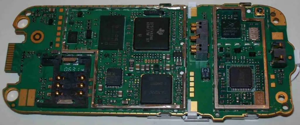
Gerber File Format

Gerber files are the standard file format used to transfer PCB design data between CAD software and PCB manufacturing equipment like photoplotters. Some key points:

  • 2D vector image format representing PCB layers
  • Contains PCB outlines, copper traces, pads, holes
  • Developed by Gerber Systems decades ago
  • Extensively used in PCB industry workflows

Types of Gerber files

  • Copper layers – Top, bottom, internal layers
  • Soldermask layers – Top, bottom
  • Silkscreen layer – Legends, symbols
  • Solder paste layer
  • Drill files – For holes

Gerber files are exported layer-wise from PCB design software like Altium Designer or KiCad before manufacturing. Each layer describes a unique aspect of the PCB design data.

Need for Online Gerber Viewers

Sharing PCB designs with manufacturing partners worldwide requires sharing large Gerber files containing the intricate board details. However, transferring and then viewing these files on local CAD software is cumbersome. Online Gerber viewers provide a quick and easy way to visualize the design and collaborate by:

  • Allowing uploads of zipped Gerber folders or individual files
  • Rendering 2D previews of the PCB instantly
  • Enabling sharing accessible links with the hosted view
  • Visualizing from any device without software downloads
  • Inspecting specifics with pan/zoom capabilities

This makes online viewers indispensable tools for PCB designers aiming to speed up design reviews, manufacturing discussions and prototyping iterations.

Features of Online Gerber Viewers

Online Gerber viewers offer a suite of features for comprehensive PCB visualization and inspection:

Multi-layer Preview

  • View individual inner and outer layers
  • Switch between layers
  • Adjust layer transparency

Measurements

  • Check dimensions and distances
  • Analyze spacing between tracks and pads

High Resolution Rendering

  • Sub-micron accuracy
  • Captures fine features and geometries

Annotation Tools

  • Draw, add text, shapes on layers
  • Collaborate with annotations

Cross-section View

  • Visualize multi-layer stackup
  • Inspect construction and vertical interconnects

3D View

  • Realistic 3D rendering of PCB
  • View component placement

BOM Extraction

  • Recognizes components for bill of materials
  • Exportable BOM spreadsheet

Design Rule Checking

  • Automated DRC runs
  • Highlights potential violations

File Conversion

  • Output edited files in PDF, image formats

Sharing and Collaboration

  • Share links with views for feedback

The range of analysis, inspection and collaboration features offered make online tools invaluable for optimizing PCB designs before manufacturing.

Benefits of Online Gerber Viewers

Gerber Files
Gerber Files

Online Gerber viewers provide powerful advantages:

Easy Sharing

  • Hosted views allow sharing PCB design details with anyone instantly

Accessibility

  • View designs and collaborate from anywhere through browsers

Ease of Use

  • No need to install complex PCB software locally

Time Savings

  • Significantly faster design reviews and vendor discussions

Enhanced Visualization

  • Zoom into finest routing details for clarity

Team Collaboration

  • Annotate and share feedback on hosted views

Manufacturing Insights

  • Get assembly feedback from manufacturer teams

Cost Reduction

  • Avoid multiple PCB design iterations and corrections

Design Validation

  • Thoroughly inspect designs prior to fabrication

By facilitating instant PCB visualization and feedback online without software hassles, significant time and cost savings can be achieved during product development.

Top Online Gerber Viewers

Many free and paid online Gerber viewers provide capabilities for PCB inspection. The most popular choices are:

Gerber-Viewer.com

  • Free online viewer with basic PCB viewing features
  • Good rendering but lacks advanced capabilities

ViewMate

  • Basic layer viewing along with annotations
  • Limited collaboration features

JustGerb.com

  • Free online tool with good visualization
  • Email sharing and simple measurement

Tracespace Viewer

  • Advanced 3D rendering engine built on WebGL
  • Capabilities like DRC, BOM, step-and-repeat

CircuitHub

  • Feature-rich online viewer integrated with PCB services marketplace
  • Design reviews, quotes, orders managed through platform

Altium 365 Viewer

  • Tightly integrated with Altium Design tools
  • Enables real-time design collaboration

PCBWeb Viewer

  • High performance online viewer tailored for fabrication needs
  • Extensive layer control and visualization options

The ideal choice depends on specific workflow needs ranging from basic sharing to tight design tool integration.

Using Online Gerber Viewers Effectively

To leverage online Gerber viewers optimally for PCB needs:

Prepare Files

  • Export separate Gerber files for copper layers, soldermask, silkscreen, drill and routing

Check Plot

  • Always cross-verify exported layers against design software plot

Upload Relevant Layers

  • Avoid uploading irrelevant auxiliary layers

Inspect High Resolution

  • Zoom into routing layers to check track widths and spaces

Leverage Layer Control

  • Isolate or switch off layers for clarity as needed

Use Annotation

  • Add shapes, text to highlight areas of interest

Capture Images

  • Use screenshot tools to save images of key areas under review

Enable Design Reviews

  • Share hosted view links with fabrication partners

Iterate Rapidly

  • Use online inspection to quickly finalize designs

Employing online viewers strategically helps identify issues early, enables collaborative reviews and reduces overall design cycles.

Limitations of Online Gerber Viewers

dXf to Gerber converter

Despite immense capabilities, online Gerber viewers also have certain limitations:

  • Lack advanced PCB editor features only available in full desktop CAD tools
  • May not render some component 3D models or pad shapes accurately
  • DRC checks may not be as exhaustive as desktop tools
  • Annotation capabilities are limited compared to design software
  • Can handle moderate sized designs but very large boards can get slow
  • Proprietary data not fully secured compared to local viewers
  • Require active internet connection unlike standalone tools

Online tools complement but cannot fully replace advanced desktop PCB design software yet. Secure data transfers and downloads are recommended for proprietary designs.

The Future of Online Gerber Viewers

Online Gerber viewers are expected to evolve with:

  • Enhanced Real-time Collaboration – Allow multiple stakeholders to visualize and annotate PCB designs seamlessly in real-time.
  • Augmented Previews – Offer augmented layer previews combining 2D, 3D and x-ray views for enhanced visualization.
  • Design Editing – Move beyond just visualization to limited PCB editing capabilities.
  • Deeper CAD Integration – Tighter integration with popular PCB design tools for seamless workflows.
  • Advanced DRC – Faster and more sophisticated design rule and electrical checking algorithms.
  • BOM Integration – Intelligent data extraction to build component lists and Bom directly online.
  • Manufacturing Integration – Close integration with manufacturing through ordering and production tracking.
  • Scalability – Ability to handle larger designs, higher data volumes as internet speeds increase.

As online tools gain more sophisticated capabilities, they are poised to become integral hubs connecting PCB design, analysis, collaboration, manufacturing and production workflows in the future.

Conclusion

Online Gerber viewers provide a quick and easy way to visualize, inspect and collaborate on PCB designs through an accessible online platform. They fill a vital need in electronics product development by facilitating rapid design reviews, discussions with manufacturers and speeding up iterations required before finalizing board fabrication. While lacking advanced editing features of full desktop tools, online viewers in their current form complement design software through key capabilities like multi-layer previews, annotations, measurements, screenshots and online sharing. With continual improvements in real-time collaboration, augmented views, design rule checking and deeper integration with PCB CAD, online Gerber viewers hold immense potential to enhance and integrate the electronics development workflow.

What is Online Gerber File Viewer? – FQA

Q1. What file format do Gerber viewers allow inspecting online?

Gerber viewers enable viewing Gerber files – the standard file format for transferring PCB design data to manufacturing containing 2D CAD information of the board.

Q2. What are the key advantages of online Gerber viewers?

Benefits include easy online sharing, accessibility through browsers, quicker design reviews and collaboration, rapid iterations and avoiding multiple board fabrication cycles.

Q3. What are some examples of popular online Gerber viewers?

Top online Gerber viewers are Gerber-Viewer.com, ViewMate, JustGerb.com, Tracespace Viewer, CircuitHub Viewer, Altium 365 Viewer and PCBWeb Viewer.

Q4. What are some limitations of online Gerber file viewers?

Limitations are lack of full editing features in desktop tools, inability to handle very large designs, lower data security than local viewers and need for active internet connection.

Q5. What future improvements are expected in online Gerber viewers?

Future advances include enhanced real-time collaboration, augmented layer views, limited editing, tighter CAD integration, advanced DRC/DFM analysis and closer manufacturing workflow integration.

How to find and use an Online Gerber viewer

Viewing modes

You can open the PCB online Gerber file viewer with PCB editor software in two modes: online or offline.

In online mode, you can open the software directly from the PCB editor software. The two are running at in same time. You can use them independently or each other for cross-checking purposes. For example, you can view the Gerber file in PCB editor software, change some information and then switch to online Gerber viewer to review how it affects the Gerber file. You can also check how your layout looks like after printing it out. Or you can do all three at the same time. You can save the layout to an external file (it is handy if you need to modify/edit it in another software) and then reload it to PCB editor software.

You must open the Gerber file with PCB editor software offline, then open the online Gerber viewer application separately. We use them independently, but no communication between them. Once you complete your layout in the PCB editor software, you can save it in Gerber file format. Then launch the online Gerber viewer application to view and check your layout in the Gerber file. It is also handy if you need to modify/edit it in some other software.

The following sections will show you how to use both modes, step by step.

Online Gerber Viewer

Step 1: open PCB online Gerber viewer with PCB editor software

(1) Online mode:

  1. Launch the PCB editor software you are using and load a Gerber file to open the layout
  2. Go to view>More>Online Gerber Viewer, click it to launch it
  3. The system will display the layout in the online Gerber viewer

(2) Offline mode:

  1. Launch the PCB editor software you are using and load a Gerber file to open the layout
  2. Optional: use the Plus icon to create a new folder and name it as you like
  3. The system will display the in the online Gerber viewer

(3) Close online Gerber viewer:

  1. Right-click the item highlighted in the following screenshot and selected Close from the popup menu
  2. You will see the Gerber file in offline mode in PCB editor software. You can edit it there

Step 2: edit specs online

  1. Select Online Gerber Viewer>Edit>Edit Spec to edit the single layer, multi-layer, Excellon drill file, or screen dump data.
  2. You can use the following options to change any information you want:

The option arrow keys will allow you to zoom in for more details, so you can see exactly where it needs modification.

Step 3: print out the modified Gerber file

  1. Select Online Gerber Viewer>File>Print, set printing options.
  2. The system will print out the modified Gerber file automatically. Before printing, check if there is enough space on the paper to print it out, or you need to adjust page size in your printer driver settings.
  3. We will refer the virtual printer to as โ€œGerber Viewerโ€ by default, but you can change it to whatever you like in the Printer name:
  4. The system will print out the Gerber file on paper:
  5. The Gerber viewer automatically connects to the directory of the Gerber file on your computer and shows you the image of the printout:
  6. Close online Gerber viewer:
  7. Right-click the item highlighted in the following screenshot and select Close from the popup menu:
  8. Note down your modified Gerber file in a location you can find it easily later.
  9. Transfer your modified Gerber file to the PCB editor software, open it to review it.

Layout mode

FULL PCB MANUFACTURING Quote

2D Layout Viewer

You can open with online gbl file Viewer in the 2D layout view. It is useful to view your layout on a two-dimensional plane, without the PCB design software, by just using an online Gerber viewer. To do so, go to file>View>Online Gerber Viewer>2D Layout Viewer.

This view works similarly to Windows Paint, where you can draw lines and shapes with your mouse. If you have been making PCB layouts for a while, then this will be familiar to you. You can change the background color with the checkbox in view>Color>Back; enter a color code there.

The user interface is simple and easy to use. You can drag the screen around to look at the layout from different angles. You can also right-click on the screen or any object and select various options from the popup menu.

3D view

You can use a 3D Gerber viewer to see your design from all angles in this model. To enter 3D view, go to view>3D View or press the F3 key. You can use Alt+Arrow keys to pan around the screen, scroll up/down using the up/down arrow keys on the keyboard and rotate by pressing the left/right mouse button on it.

Zoom

Zooming in and out was a common function in the past. In 2D, you can use Ctrl-Z and Ctrl-Z to zoom in/out, respectively. In the 3D view, you can use the mouse wheel to zoom in, the Ctrl+Plus key to zoom out, or the Alt+Plus key to reset. You can also enter the value through the keyboard by pressing NumLock once and the letter you want to change next time.

Projection

This function works in the 3D mode that you can use to create a perspective view of your PCB layout. To enter projection view, go to view>Projection. If you want to restore the default setting, go to Projection>Preset and select default (keep existing settings).

The zoom must be off when entering projection view. You need to switch it on after entering the new settings.

Snap to Grid

You can superimpose the grid over your layout to make drawing the tracks easier. The grid is not visible when working directly on the design, but you will see it in editing mode or viewing the design. It is useful for making sure your track widths and spacingโ€™s meet their manufacturing tolerances. To set up a grid:

  • Go to view>Grid and select Grid (in v0.16, the grid is not available by default, you need to select it from view>Grid menu or View>More>Grid). It will add a blue grid line to the layout.
  • To remove the grid, repeat step one but choose Grid (Off) instead.
  • If you have made changes to your layout and want to view them again with a grid on, go to view>More>Grid and select Grid (Recalculate).
  • To change the size of your grid, go to view>Tools. There are many sizes available. If you want to calibrate your grid, go to view>Tools>Calibrate grid.
  • The grid display will only update if you zoom the view in or out or change your layout.

You cannot edit the directly in the design view. 2 ways are available to do it:

  1. Use view>Snap to Grid command to overlay a grid over the design.
  2. Use the Traces command to draw a rectangular grid that you can edit. The grid cells will appear as you draw and will also appear when you turn off the grid.

You must draw the rectangle within your design view. It must completely fit within the boundaries of your layout (not outside and not overlapping any object). It cannot extend past the last line or first line of the design.

Alignment

This function is useful for aligning objects on the same layer in the same direction. To align something vertically, choose View>Alignment and select Vertical or Horizontal. For horizontal alignment, choose View>Alignment and select Horizontal. To align objects in an angle to cross each other, select view>Alignment, select Angle or Normal, and click on your track or object. You can use our button to do it.

The define button is at the bottom of this dialog. You can click on the button to open the following dialog:

Line up two grids with each other. The first grid is the one that goes through your reference point. Suppose you want to align objects vertically or horizontally with each other, drag-and-drop one of them into the first column. Then drag the second object into any column, and click the Match with First/Second Grid button if needed.

The Angle alignment is useful when you want to align objects at an angle to cross each other. For example, making a wire track on the bottom layer with 45-degree alignment will cross another wire track on the top layer.

Import Layout

If you are working on another layout in the PCB editor, I recommend you import your layout with this function to check your design easily. To import your layout, go to file>Import Layout. The โ€˜Import Layoutโ€™ dialog will appear. Then go to the directory where you saved your design and select the file.

Export Layout

You can export your layout in Gerber or Import it into another PCB editor with this function. To export, go to file>Export Layoutโ€ฆ The โ€˜Export Layoutโ€™ dialog will appear. Select the target directory where you want to save it, then enter a name for your file in Output File. You can also select the output format through File Format.

Snap Resolution

The resolution determines the minimum increment that tracks. You can change it by going to view>Tools or enter a value for this parameter directly into the toolbar. Set this value in one mil (1/1000 inches). The default setting is one mil, and there is no other significant increment. The highest possible setting will be 0.0187โ€ (8 mils).

Draw Mode

To switch between the various drawing modes, go to view>Draw Mode. There are also options for scaling the view. The choices are Independent or Relative scaling. With independent scaling, you scale each object separately to see whether they are in proportion to one another easily. Relative scaling scales everything according to its distance from the viewport (the boundary around your layout) and does not take objects into account that are outside of it (i.e., off-screen).

To switch to a different drawing mode, check the appropriate checkbox above the list, and select a drawing mode from the drop-down menu. There are also options for scaling the view. The choices are Independent or Relative scaling. With independent scaling, you scale each object separately to see whether they are in proportion to one another easily. Relative scaling scales everything according to its distance from the viewport (the boundary around your layout) and does not take objects into account that are outside of it (i.e., off-screen).

Line Style

To change the line style, go to view>Line Style. There are many types of lines available. Please visit view>Line Style for details.

Text Style

To change the text style, go to view>Text Style. There are three text styles available, each with different options. For more information on how to use them, refer to the Text section of this tutorial.

Hatch Pattern

To change the hatch pattern, go to view>Hatch Pattern. There are many types of hatch available. Please visit view>Hatch Pattern for details.

Layer

To change the layer, go to view>Layers or click on the Layer button in the toolbar. The layers dialog appears, then you can use it to switch between layers, set the layer color and properties.

Layer Color

You can use the view>Layer Color command to change the color of your active layer. The Layer Color dialog appears, then you can choose either Solid Color or Gradient. If you choose Gradient, you need to set Start and End colors.

Layer Properties

In the layers dialog, you have a list of all your layers. In there, you can check the color for your layer. If you click on the triangle beside the layer name, a dialog will appear where you can set properties for your layer. You can set Layer Name, Description, Orginal Size, and Position.

PCB online Gerber viewer supports PCB editing functions. It includes cube selection, layer stacking determination, wiring management, data transmission line generation, hole drill generation, and auto-printing.

PCB online Gerber viewer supports drag-and-drop, which makes the different editing functions very convenient.

PCB online Gerber viewer supports hotkeys for easy access and quick operation.

Online PCB Graphic Tool

A PCB fabrication service company has developed an online PCB graphic tool with a very simple user interface. This tool allows you to view your Gerber files anytime and anywhere you go, with the facility of storing them on the companyโ€™s live web page. It is just a normal jpeg image file that you have uploaded to the web pages. You can also download the Gerber viewer free of charge. Working with global manufacturers such a RayMing PCB and Assembly will help ensure that your product will be up to standard since they are using some of the best tools as Gerber viewer.

To open your Gerber file, first, you should download it from your PCB manufacturer or reseller. Then open the Gerber file with GERBER_FILE_WIZARD. To open the dialog, you need to go to file>Open. The โ€˜Openโ€™ dialog will appear. If you have already downloaded your Gerber file, select the directory where you stored it and enter its name into File Name. Then click on Open

To view your Gerber file, first, you should create a file, then open the Gerber file with GERBER_VIEWER. To open the dialog, you need to go to file>Open. The โ€˜Openโ€™ dialog will appear. If you have already created a file and opened the Gerber file in it, click on Open.

Gerber Viewer

Gerber Viewer is an editor for viewing Gerber files which one writes in C++. It is a cross-platform tool, so it will support all platforms, including Linux and Mac OS X. You can view your Gerber files online instantly after downloading the Gerber file from your PCB manufacturer or reseller. Just click the button, and the Gerber file will appear in your browser. You can then download it or save it into your local system.

There are free online Gerber viewers who support viewing both single and multiple Gerber files. You can view these files very easily after you have downloaded them from your PCB manufacturer or reseller. You can drag the file onto the window. If you want to zoom in, double-click the window, or use [Ctrl] [Mouse wheel].

Online Gerber Viewer

You can view your Gerber files in this tool anytime and anywhere you go, once you have captured them with your camera or scanner, and then uploaded the image to their website, where they have a special section for PCB design projects.

The first two are free online Gerber viewers that allow you to view your Gerber files anytime and anywhere you go. After you have captured them with your camera or scanner, upload the image to the website and then view them at any time.

Eagle CAD

Eagle is a combined schematic and layout editor and is part of the Electronics Workbench (EWB) suite (www.electronics-workbench.com). Working with schematics and boards in Eagle breaks down into three steps: creating a new design, modifying it, or backing it up for later editing.

Eagle CAD Block Editor

It is a free online component editor by Universal Devices Inc. that makes a wide range of embedded system products, including the MAX232 serial I/O IC, MAX4630 temperature sensor IC, and MAX6675 absolute temperature sensor IC. So you can use this block editor to view your Gerber files at anytime and anywhere you want as it supports both viewing and editing of these files and viewing of schematics and boards made by them too.

Eagle CAD Block Editor can view the schematics and boards created by Eagle CAD.

This component editor can easily view the Gerber files edited by Eagle CAD as it automatically supports viewing of edited Gerber files.

SparkFun

The schematic capture and board layout software used in the SparkFun Electronics open-hardware library is OpenOffice OrgChart (www.openofficeorgchart.org). It is a schematic capture and board layout software developed by OrgChart Team for editing and drawing organization charts. This tool does not support Gerber file viewing, but it supports the open-source Gerber file format, which is not viewable in most tools or online viewers.

Eagle Library

There is an online library for eagle parts called eagle lib (www.eaglelib.net). It is a library of Eagle parts and contains 3D models for many components. You can view your eagle parts anytime and anywhere you go. Once you have captured them with your camera or scanner, you can upload them to this site.

This library also hosts the eagle file format (EAGLE), used to store board designs made in Eagle. This library supports many different PCB manufacturers and PCB designers too.

Thus, this library will also store your Gerber files if you mark them in EAGLE file format.

DesignSpark PCB

There is an open-source PCB design software called DesignSpark PCB (www.designsparkpcb.com). You can easily create your designs with drag and drop components and then export them into DXF files compatible with many PCB manufacturers.

You can easily view the Gerber files created by DesignSpark PCB by Sparkfun, Eagle CAD, and eagle lib.

But it is challenging to view them in most online tools or website viewers because Sparkfun, Eagle CAD, and eagle lib support the open-source Gerber file format, which is not viewable in most tools and website viewers.

Max + MBE + BEE

Max is a programming language created by MIT which helps create interactive applications. The development environment uses the Processing language library, which depends on Java.

We can find Max on many different sites, but the best one is the original site designed to teach programming to artists and non-technical people.

The online version of Max is an interactive board editor released under the GNU GPL. It uses the Processing language library, which depends on Java.

Processing

Processing is a programming language created by MIT which helps create interactive applications. The development environment also uses the Processing language library, which depends on Java.

We can find Processing in many different sites, but the best one is the original site designed to teach programming to artists and non-technical people.

Conclusion

The future of PCB design and manufacturing requires the use of open-source Gerber files. They will allow anyone to share their designs with anyone else and provide a way to view those designs for those who donโ€™t have the right equipment or software. The ability to share Gerber files means anyone can create and view open-source PCBs.

To create a new design, you must view the Gerber file, part of your design. Without Gerber file viewing in CAD tools, it wonโ€™t be easy to develop new designs.

The old way of storing the Gerber files on a website is no longer a good solution as most people only have access to a few websites. If a person wants to view your Gerber files, they must know where they are and how to look for them.

What is an IC board?

ic board

An IC board is a type of printed circuit board assembly (PCBA) that contains integrated circuits (ICs) mounted on the board. Typically, you solder an IC to the surface of the PCB assembly and wires attached to it. This article will tell you everything you need to know about IC boards. It includes identifying common ICs found on boards, their applications, and what types of damage can happen to them.

How do IC boards work?

IC on boards work using components and connections. Depending on the requirements, they come in different sizes and forms. But, most contain several interconnecting wires that link the components together.

They also require mechanical support for the wires that link components and those that go outside to meet other devices. The board can provide the support or an outer frame that holds those internal wires and those external ones.

In most cases, IC boards have contact pathways that keep the components from being electrically connected. It is usually the case with outer frames as well as the board. Imagine a circuit without these pathways, and it will be hard to imagine how they work at all.

The main thing to remember about IC boards is that they contain several connections. These links connect link various components together. They require mechanical support, both internal and external, to function properly.

Types of IC boards surface mounts

FULL PCB MANUFACTURING Quote

It is a system of the most modern electronics where you mount the different elements on a common base. So, one can easily remove and place them anywhere on this base and move it around.

It is the type of board where you mount six or more chips on each side, but not immediately next to each other, but of course, they are just adjacent to each other.

We use this method when you mount only four or five chips. They are all located on the same side of the board and not one next to the other.

The method we attach all chips directly to a substrate allows us to connect them to the outer circuit by using conductive areas that run along their sides.

Mechanisms of IC boards

The main reason for using IC boards is to offer a stable and durable base for devices, such as semiconductor components, which need to connect.

We use IC boards for installing these devices or components. Also, we use them for making connections between two integrated circuits since they are the main reason for connecting these devices.

We install IC boards to link components that we may operate by using a single power supply instead of several power supplies. It is to link devices that we cannot change if something goes wrong with them. The main purpose is not to change its operational parameters at any cost.

Purpose of IC boards:

With today’s modern technology and modern electronic devices and components, the use of IC boards has become part and parcel of almost all electronic systems, especially when we speak about small or medium-sized electronic systems.

The only difference is that in some circuits, there is no need for using IC boards. Since they are already complete and complete, they need to look for new ways to improve them is to introduce new components or elements.

Can we use IC boards for producing consumer products? Yes, IC boards are compatible with consumer products.

We use these boards in modern electronic appliances because they come in smaller sizes that are compatible with various small electronic devices. This feature allows the use of them in special kinds of appliances that millions of people can use worldwide, which was not possible before the invention of electronics.

However, the main reason is that the IC boards are very cheap, so consumers can easily introduce these devices.

Can you use IC boards for industrial products? Certainly, IC boards are now used in industrial products as well. Most of these components are not dependent on each other now, so they do not affect the rest of the system if one fails.

Microcontroller Application Areas

A microcontroller is a small computer chip (IC) designed to control machines’ speed, direction, and other mechanical tasks. We use microcontrollers in industrial, medical, automotive, consumer products, robotics, and other electronics.

The heart of any machine is its microcontrollers; this is where all the significant electrical signals come from and go. We also use the microcontrollers for anything in the machine function. A manufacturing line may use a microcontroller to signal when to start the next circuit, while another may use one to help with the assembly process. The most common application areas are in the following:

  1. Automation โ€“ We can use these components in many forms of machines. It includes assembly lines, packaging lines, printing machines, and robotic devices. We can integrate them into automated equipment or directly wire them into the machinery itself.
  2. We use industrial Control in industrial control systems. It includes automated control systems, industrial robots, and factory automation.
  3. Medical โ€“ We use ICs for medical equipment such as X-Ray machines, Endoscopes, and blood pressure machines. Company physicians use them for small patient monitoring systems or send them to the machine’s manufacturer to integrate them into it.
  4. Mechanical – These are usually found in assembly line equipment like robotic arms, conveyors, and pick/place units (aka robotic hands).
  5. Vacuum โ€“ We usually find them in specialty machines for maintaining or servicing vacuum systems, such as vacuums used in warehouses or food processing plants.
  6. Test โ€“ We use them in measuring instrumentation equipment, test chambers, temperature control devices, and other measurement instruments.
  7. Misc Electrical โ€“ We find them on the back of electrical equipment that requires large amounts of power to control equipment like fans, lights, and electrical gates.
    8. Industrial โ€“ We use them in industrial applications like forklifts, industrial robots, and industrial computers.

Application of ICs on PCBs

ICs are usually embedded with leads to attach to the circuit board. Three main types of application patterns that we can find on the circuit boards:

  1. Surface Mount – This is the most common type of application used for most ICs. We usually find them on equipment where space is at a premium, such as printing machines, medical equipment, packaging machinery, etc. We can find this type of circuit board with any IC on it.
  2. Through Hole – This type of PCB usage is not as common as surface mounted, but we use it in more complex PCBs requiring lots of IC connections, usually on less space-critical equipment.
  3. Hybrid – This type usually uses a mix of both through-hole and surface mount connections to the IC.

Common IC parts:

  1. Ceramic: These parts contain ceramic and are usually found in small and medium devices (5mm and larger).
  2. Thin Miniature Metal-Can: We can attach these parts to Integrated circuits integrated circuit using wire leads or fine solder bumps. We use them for power amplifiers, voltage regulators, DC-DC converters, oscillators, etc., where size is critical.
  3. SMD: Small Surface Mount Device. We commonly find these devices in logic or memory circuits.
  4. Through-Hole: We typically find these parts in large devices (5mm and up). We use them mostly in device chassis, power supply units, and output circuits of MOSFETs, Op-Amp chips, etc., where space is at a premium.
  5. BGA: Ball Grid Array. We use these parts for components that require the highest reliability and performance, like computers, digital TVs, etc. BGA’s can be anywhere from 25 to 500 micrometers in size.
  6. Flip Chip: These parts are usually small components (5mm and up). We typically use them in devices like D/A converters, memory circuits, microprocessors, and microcontrollers.
  7. QFP: Quad Flat Pack. We find these components in the most complex devices in electronics, like cell phones, computers, etc.
  8. CSP: Ceramic Small Package. We use these parts in complex devices like cell phones, computers, etc., where space is premium or needs to be very small but still contain many components.
  9. LCC: Low Profile Surface Mount Device

A PCB must go through four steps:

There are different types of designs like custom design and standard design. When designing a PCB, it is normal for engineers to choose one of the two. However, in some cases, they also need to use both methods. For example, when designing a circuit board with soldered components, they need to use standard design since they are using soldered components, all of which have standard designs. It is only in the case of custom design that engineers need to use it.

If an engineer uses both methods, he must know how to work with both since they are both different. So, he must know which tools are essential in each one of these steps. He must also learn how to use each tool for completing the design process. An engineer can work with them in a certain way or another depending on his knowledge about the tools and their functions.

To use a design tool, an engineer must first know how it works, and then he must look for a good user guide that will reveal the correct ways of using these tools. After that, he should start working with it.

A PCB designer usually uses a CAD system to produce the designs of boards. These CAD systems are generally very powerful, and they can produce incredible results. The main purpose of using CAD systems is to design the board and then send them to manufacturers.

How do I install IC?

An IC contains leads and leads pinout. Also, it is very useful to spend some time learning about the various leads before installing the IC. A lead contains an internal connection that connects to another pad on the PCB or another device.

Leads are usually connected to the IC’s pins using solder but can also connect through wire bonding or wire-bonding pins via metal plating onto the leads.

Sometimes, as an alternative, we can attach ICs to the PCB utilizing epoxy or resin.

The first step should be to prepare the PCB and other equipment, such as power supply modules and conduits for connection. The second step should be choosing and designing the IC and connecting components and wiring (other ICs or parts on the PCB or devices like diodes). The last step should be to attach all components and connections with solder.

IC boards installation process

  1. Read the instructions carefully before beginning the exercise to ensure that you understand them well and do not leave anything out when preparing for assembly or application.
  2. Use the proper tools when soldering. We should use a soldering iron with a temperature between 220 and 260 degrees Celsius since the higher temperature can damage electronic components and materials in many ways, including causing excessive heating in terms of causing insulation breakdowns or thermal shocks.
  3. Be careful not to scratch the leads by using something like a metal tweezer, which can cause the leads to break off or get damaged.
  4. Do not touch the pins with anything that can cause static electricity (e.g., hairdryer).
  5. Make sure that you do not get anything (i.e., solder, flux, etc.) on the contacts of the IC; otherwise, it will get damaged and become useless after some time.
  6. Do not leave any excess solder on the leads, as it can cause a short circuit or cause problems with the operation of the device.
  7. Do not bend, twist or expose ICs to excessive heat, moisture or humidity during installation and use.
  8. After attaching an IC, do a test run before using it in another device or circuit to ensure that everything is working correctly.

Types of damage to common ICs

Two main types of damage can occur to ICs on PCBs – Physical Damage and Electrical Damage. However, many other types of damage to ICs do not strictly fall into either category (e.g., misapplication, inappropriate handling, etc.).

Physical damage includes circuit board flexing caused by flexing flex. It results in the flexing star points (small metal pins connecting between the board and the IC) breaking or bending.

Electrical damage affects the solder bond between the leads of the IC and the PCB pads. It can cause an open circuit or short circuit. Short circuits are usually bent leads connecting to other pads, while open circuits have broken leads.

You should take special care should when handling ICs since they are very sensitive to mechanical shock. The reason being is that an IC is very fragile and small, so it can easily get damaged if dropped or hit by debris.

ICs themselves are sensitive to certain chemicals. For example, one can damage some ICs by exposure to solvents. Be careful not to put them in places where they can get exposed to chemicals.

We should use care when installing the IC on the circuit board. Firmly press them down onto their pads with your index finger or thumb after you have applied flux to the pads and leads of the IC.

Some ICs contain ceramic packages, and we should handle them with care. They are very fragile and can easily break if dropped or struck by debris.

Some ICs contain polysilicon package and can break if looked at directly. It happens because the package will heat up significantly.

You should take care when handling these types of ICs as they can easily get broken or broken off during handling and overheat and potentially become damaged due to excessive heat.

Choosing a suitable IC board

The main reason for using these boards is to link components that may want to operate using a single power supply instead of several power supplies. It is to link devices that we cannot change if something goes wrong with them. The main purpose is not to change its operational parameters at any cost. In addition, IC boards have different designs that depend mainly on the size of the components they will include and how easy they are to use or manufacture.

A PCB designer must be knowledgeable about these designs since they are the ones that will help them to select the best one for creating the PCB. After considering this, he must also know how each design works.

However, to use these designs properly, an engineer needs to analyze all options first and then make correct choices. When an engineer chooses a certain design over another one, he needs to know how it works and other designs’ features.

In addition, the manufacturing process of each design is also essential when choosing a certain type of design. In this way, an engineer can select the most suitable one that is easy to manufacture. We highly recommend that he consider all things before deciding on a specific type of design.

The first step is to choose the best design for an IC board. After that, he can go to the second step, choosing how he will manufacture the board.

All these steps are quite necessary, so the engineer should know them well. Also, he should learn how to implement them correctly.

Things to keep in mind

  • To do the IC board design, first, you should take some time to think about the whole system that will include this board. Then you can start to consider different kinds of designs that we can use for this purpose.
  • After considering all these points, you must start with one of these designs based on your choice. You should start producing the designs with CAD systems.
  • In the end, your design is ready for manufacturing to prepare all these files for manufacturing process production.

IC board manufacturing process

Choose the best design for an IC board

The first step of producing an Integrated Circuit board is to choose the best design for it. To make sure that everything will be fine, we recommend that you consider all details before deciding. You can consider the type of components you will use, the number of these components included in the design, and how much space each component will need. When you have all these factors in your mind, you can make a good choice.

Selecting a PCB manufacturing company

After creating a PCB design suitable for creating a particular product, a PCB designer must now decide how to manufacture this board. You must make this decision carefully because there are different choices. The main factors that you should consider when choosing this manufacturing company are the types of manufacturing processes they use, their production capacity, and the cost of their services. Having a global manufacturer such a RayMing PCB and Assembly will help ensure that your product will be up to standard since you are contracting them for an assembly job.

Selecting each design to manufacture

When the PCB designer selects a certain design, he must know the manufacturing process. This process is quite essential. Otherwise, he may choose the wrong one for this product or create problems in its production. These problems can occur when he does not consider the entire process of the board’s manufacturing process. If this happens, he will make mistakes in his design and its production.

Selecting suppliers for components

After selecting the PCB manufacturing company and designs, an engineer must establish a list of suppliers for components. Then, he can ask them to provide him with what he needs in his design.

Establishing an assembly process

After receiving all components of the product, an engineer must establish an assembly process to test the functionality of this product. He must also test the boards to see if the manufacturing process is correct and working fine.

Final steps

The last step of producing an IC circuit board is checking all aspects of the component’s design. This step is quite essential because it will help the engineer to use this product correctly.

To choose a suitable design for creating a specific product, an engineer should consider all factors relating to its manufacturing.

Conclusion

The essential components needed for any electronic system, such as an IC board, come from manufacturers worldwide. Almost every producer is selling printed circuit board designs which you can find in several online shops.

Nowadays, there are also specific boards that you can find, designed especially for the main parts of specific electronic systems and not just for general use.

There are many different characteristics of printed circuit boards that differ between the various models. It makes it very important to consider what you need before buying any of these boards. Because no matter how many features it has, if they are not necessary for your specific purpose, you will just be wasting your money.

Why Need EMI Shielding in Electronics ?

Introduction

EMI or electromagnetic interference shielding refers to techniques used for suppressing electromagnetic interference generated by electronic devices. EMI shielding blocks electromagnetic waves from reaching or escaping the device using conductive materials that reflect or absorb radiated energy.

This article provides a comprehensive overview of EMI shielding including:

  • Basics of electromagnetic interference
  • Need for shielding electronics
  • Shielding principles and materials
  • Shielding methods and design
  • Shielding measurement
  • Applications and trends

Understanding EMI shielding concepts enables designing robust electronic products that function reliably by containing interference.

Basics of Electromagnetic Interference

Electromagnetic interference (EMI) refers to disturbances caused due to unwanted generation, propagation and reception of electromagnetic energy that can potentially degrade the performance of electronics.

Sources of EMI

  • Switching signals and clocks
  • Power supply rectification
  • Data and control buses
  • High speed serial links
  • Displays and touch interfaces
  • DC-DC converters
  • Motors and relays

Effects of EMI

  • Increased error rates in data transmission
  • Noise on audio and video signals
  • False switching and spurious behaviors
  • Degradation of signal integrity
  • Equipment malfunctions and shutdowns

With greater computing speeds, closed system architectures and sensitive analog interfacing, EMI mitigation through shielding becomes vital for reliability.

Need for Shielding Electronics from EMI

Electronic Shielding

Shielding is essential for ensuring proper functioning of electronic equipment due to:

Susceptibility Requirements

  • Electronics need protection from external interference sources

Emission Requirements

  • Prevent device emissions from disrupting other equipment

Regulatory Compliance

  • Meet EMC/EMI standards for electronic products

Signal Integrity

  • Guard noise sensitive analog signals and sensor interfaces

Safety

  • Avoiding equipment malfunctions and shutdowns

Security

  • Contain compromising emanations from circuits

From laptops to medical devices, automotive electronics to LTE basestations, shielding helps electronics operate reliably and safely by suppressing interference.

Shielding Methods and Materials

EMI shielding aims to contain EMI through reflection, absorption or diffusing the emitted energy using conductive materials surrounding the source. Common shielding methods include:

Faraday Cage Shielding

An enclosure made of conducting material that blocks external fields. Works by induced surface currents cancelling incident fields.

Conductive Coatings

Paints loaded with conductive fillers like nickel, copper or carbon particles that reflect/absorb EMI when coated on plastics.

Conductive Plastics

Plastics mixed with fillers like stainless steel fibers, carbon particles or nickel coated graphite that provide shielding through absorption when molded into enclosures.

Board Level Shielding

Small metal cans soldered onto PCBs enclosing components needing isolation. Effective for blocking high frequency noise.

Cable Shielding

Foils or braided mesh surrounding cables that isolates signals from external noise pickup/radiation.

Component Shielding

Shielding integrated into component construction. Examples include metal core PCBs, shielded connectors, absorptive cables.

EMI Gaskets

Conductive elastomer gaskets placed between metallic chassis/covers that compress during closure to block EMI leakage through gaps.

Optimal shielding combines multiple techniques tailored to the frequency range, emissions sources, mechanical design and cost.

Shielding Materials

Materials commonly used for EMI shielding include:

  • Metals โ€“ Steel, nickel, copper, aluminium, tin
  • Conductive paints โ€“ Nickel/copper filled latex, epoxy, acrylic
  • Conductive coatings โ€“ Vacuum deposited aluminium on plastic
  • Conductive plastics โ€“ ABS, polycarbonate with Ni-coated graphite filler
  • Conductive foams โ€“ Silver coated open cell PU foam
  • EMI absorbers โ€“ Ferrite tiles, carbon loaded foam absorbers
  • EMI gaskets โ€“ Conductive elastomers with silver plating

Selecting suitable materials involves balancing shielding effectiveness, manufacturability, corrosion resistance, cost constraints and mechanical needs.

Shielding Design Considerations

Some key aspects for effective EMI shielding implementation are:

Governing Standards

  • Understand applicable emissions and immunity standards like FCC, CISPR 11

Frequency Range

  • Blocking lower frequencies requires thicker, solid metal shields unlike high frequencies

Shield Location

  • Close proximity to sources provides optimal containment

Seams and Gaps

  • Minimize openings for leakage of unwanted emissions

Grounding

  • Robust grounding of enclosure using multiple low impedance paths

Filtered Connectors

  • Prevent noise coupling through shields via connectors

PCB Layout

  • Careful component placement, routing and stackups to isolate noise sources and victims

Simulation

  • Model shields and analyze with full-wave solvers to predict resonances

An optimized shielding system requires a holistic approach across mechanical, electrical and electronic design.

Shielding Performance Metrics

Shielding effectiveness indicates the reduction in radiated and conducted interference by shields and is expressed in dB. Key metrics are:

Plane Wave Shielding Effectiveness (PWSE)

Measures far-field attenuation when plane EM waves impact the shield. Important for emissions containment.

Near Field Shielding Effectiveness (NFSE)

Measures shielding performance for near-field electric and magnetic coupling. Crucial for immunity and signal isolation.

Transfer Impedance (ZT)

Determines conductivity across the shield between source and victim. Lower ZT indicates better absorption.

Insertion Loss

Measures the reduction in conducted interference from source to victim through shield. Similar concept as transfer impedance.

These parameters help evaluate material suitability and design robustness during shielding development. Shielding performance varies with frequency and needs to be validated across the spectrum.

EMI Shielding Measurement

Measuring the shielding effectiveness quantitatively helps assess design choices and improvements. Common measurement methods are:

Anechoic Chamber Testing

Full compliance testing method with antennas transmitting and receiving through the shielding barrier characterizing both plane wave and near field shielding. Provides wide frequency characterization in controlled lab environment.

GTEM Cell Testing

Uses a tapered septum transmission line to evaluate shielding effectiveness. Can test electric, magnetic and plane wave attenuation. Portable for spot measurements.

Shielded Box Method

Simple setup with noise generator and receiver placed inside and outside a shielded test enclosure to evaluate insertion loss at various points across frequency.

MESA Imaging

Scanning imaging system that maps emissions sources and propagation to pinpoint leakage points needing mitigation.

Validated measurements are crucial during prototyping to tailor the design before final compliance testing.

EMI Shielding Applications

EMI shielding is widely used in electronic products including:

Consumer Electronics

Laptops, smartphones, wearables, home appliances, game consoles

Automotive

Engine control units, infotainment systems, LIDAR modules

Aerospace

Avionics, flight control systems, communications

Medical

Monitoring equipment, implants, scanning systems

Instrumentation

Test and measurement equipment

Industrial

Automation controllers, motor drives, robotics

Communications

5G small cells, private networks, base stations

Any application where electronics need to operate reliably in noisy environments relies on EMI shielding principles implemented through careful mechanical, electrical and PCB design.

EMI Shielding Technology Trends

Advances in materials and manufacturing are expanding shielding capabilities:

  • 3D printing – Additively built metal enclosures with complex geometries
  • EMI paints – High aspect ratio carbon nanotubes for conductive coatings
  • Hybrid coatings – Composite paints combining copper and nickel for increased conductivity
  • Thin-profile shields – Flexible conductive tapes for tight space applications
  • Structural electronics – Shielding integrated into load bearing structures
  • MIT materials – Metamaterials, fractal geometries for improved absorption
  • Graphene composites – Graphene infused plastics for light yet effective shielding
  • AI-driven design – Optimizing shielding performance using simulations and generative design
  • Expanded applications – Effective shielding demands from electric vehicles, IoT endpoints and medical devices

With electronics getting more compact, efficient and operating at higher frequencies, shielding implementation is becoming more critical across application sectors.

Conclusion

As an indispensable technique for ensuring proper functioning and emission compliance of electronic equipment, EMI shielding encompasses specialized materials, design practices and measurements. Shielding methods from conductive coatings to faraday cages along with advanced materials like graphene and metamaterials provide a robust toolkit to contain radiated interference. With electronics advancement leading to increased interference susceptibility and emissions, shielding development using physics-driven modeling and AI-based design techniques promises to be a crucial competitive advantage for developing reliable, secured and compliant products.

What is EMI Shielding? – FQA

Q1. What is the purpose of EMI shielding in electronic products?

EMI shielding blocks electromagnetic interference from entering or escaping the device using conductive materials. This ensures proper functioning and meets EMC/EMI standards.

Q2. What are some common EMI shielding methods?

Shielding approaches include faraday cages, conductive coatings/plastics, board-level shields, cable shields, component shields, absorbers and EMI gaskets between metallic enclosures.

Q3. How is shielding performance quantified?

Key parameters are plane wave shielding effectiveness, near field shielding, transfer impedance and insertion loss. These determine attenuation across frequency spectrum.

Q4. What materials are commonly used for EMI shielding?

Materials used are metals like steel, nickel, copper, conductive paints, plastics, coatings, foams, absorbers, gaskets containing metallic fillers.

Q5. What are some considerations in EMI shielding design?

Considerations include applicable EMI standards, noise frequencies, shield location, seams/gaps minimization, grounding, filtered connectors, enclosure material and PCB layout techniques.

Xilinx XC7Z035-2FFG676i FPGA Price

Xilinx XC7Z035-2FFG676i

Xilinx XC7Z035-2FFG676i belongs to the Zynq-7000 family of FPGA. The architecture of the device is based on Xilinx SoC. This family of FPGA devices are integrating several features. The device is available in both double and single-core depending on the application for which it is used. The device is grounded on Xilinxโ€™s programmable logic or PS of 28nm. The device has an outstanding ARM Cortex A-9 processor that is considered the core of the device. Furthermore, these devices are having integrated on-chip memory, interfaces for peripheral connectivity, and external memory too.

Description of Processor

The processor of the Xilinx XC7Z035-2FFG676i is having four major blocks comprising the interconnects, input/output peripherals or IOP, memory interfaces, and the application processing unit or APU.

Application Processing Unit

FULL PCB MANUFACTURING Quote

The application processing unit of Xilinx XC7Z035-2FFG676i has several features such as it has single or dual-core ARM Cortex A-9 MP Cores. The ARM Cortex A-9 features comprise 2.5 DMIPS per MHz. The operational frequency range of the processor range from 667Mhz to 866Mhz for wire bond mode and flip-chip mode, it ranges from 667Mhz up to 1GHz. The APU has the capability of operating in a single processor, has dual modes for the asymmetric processor, and dual symmetric processor. The APU also has double and single precision floating points up to 2.0 MELOPS per MHz. There is a media engine known as NEON for the support of SIMD. The APU has support for the compression of code with its thumb-2. The level-1 caches are supporting separate data and instruction up to 32Kb each. The application processing unit is a four-way set associative. There is a built-in memory management unit, secure mode operation is handled with TrustZone. There is an eight-channeled DMA. The APU has support for multiple transfer types i.e., scatter-gather, peripheral to memory, memory to peripheral, and memory to memory.

Timers and Interrupts of Xilinx XC7Z035-2FFG676i

There are various timers and interrupts in the Zynq-7000 series of FPGA. The cross-trigger interface enables the triggers and breakpoints of hardware. There is trace support and CoreSight debug for Cortex A-9. For tracing and instruction, there is a program trace macro-cell. There are 2 triple counters and timers along 3 watchdog timers and a controller for general interrupt.

Memory Interfaces

The Xilinx XC7Z035-2FFG676i unit of memory interface comprises a controller for dynamic memory and an interface module for controlling static memory. The purpose of a dynamic memory controller is to extend support for DDR memories. The controller for static memory is extending support for interfaces of NAND flash, interface for NOR flash, parallel data bus, and an interface for Quad-SPI flash.

Dynamic Memory Interfaces of Xilinx XC7Z035-2FFG676i

The controller for DDR memory is multi-protocol and is being able to be configured for delivering wide access in 32 or 16 bits up to 1GB address space through the utilization of a unity rank configuration of 32, 8, or 16-bit memories of DRAM. There is dedicated 16-bit bus-access for the ECC support. The PS is incorporating associated PHY and controller for DDR comprising of its dedicated inputs/outputs. The speed support is up to 1333Mb/s for its DDR3 memory. The controller of the DDR memory is having the capability of multi-port and is enabling the system of processing a programmable logic in common access for shared memory. There is a total of 4 slave ports for the purpose to serve one as a 64-bit port that has dedicated use for the processor through the controller of level-2 cache and is configured for lower latency. For PL access, there are dedicated ports of 64-bit. There is a single 64-bit AXI-port that is common to all of the masters of AXI ports through a central interconnect.

Static Memory Interfaces of Xilinx XC7Z035-2FFG676i

The static memory interfaces of the Xilinx XC7Z035-2FFG676i are having support for external static memories as well. There is a data bus of 8-bit SRAM that can extend support to 64Mb. There is a NOR flash of 8-bit supporting till 64Mb.

Interconnects

There is a multi-layered interconnect in Xilinx XC7Z035-2FFG676i which is responsible for connecting IOP, interface unit of memory, APU, and PL. This interconnects supporting numerous master-slave transactions simultaneously and is non-blocking. The interconnect is fashioned in a way that it has latency for masters e.g., the master of ARM CPU is having displacement paths to reach memory and the masters that are bandwidth critical like PL masters are having higher throughput connection for slaves along the way they require to communicate. The regulation of traffic can be easily made through interconnecting with its QoS block. The QoS is featuring the regulation of traffic generated through CPU and DMA controllers.

Programmable Logic of Xilinx XC7Z035-2FFG676i

The key features of programmable logic or PL of the device include having a configurable logic block or CLB, 8 lookup tables in every CLB for distributed memory, and random logic implementation. The memory lookup tables are also configurable in two 32-bit block RAM or single 64-bit block RAM. These lookup tables can also be configured in the form of the shift register.  There are sixteen flip-flops through every CLB. There are two 4-bit adders in the cascaded mode for featuring arithmetic functions. The block RAM is of 36Kb.

Debug Ports

2 JTAG ports could be combined or utilized individually. Whenever combined, a single port is utilized for the ARM Cortex A-9 processor downloading of code and for the operations of run-time, PL debugs PL configuration and logic analyzer that is pro-embedded. This is enabling apparatuses like the software development kit of Xilinx and ChipScope Pro Analyzer for sharing a sole cable for downloading from the Xilinx database. Whenever JTAG ports are split, one of its ports is utilized for support of PS encompassing direct entree to the interface of ARM DAP. This interface of CoreSight is enabling the utilization of ARM acquiescent to correct and its software development tools like development studio 5. Other of the JTAG ports could be utilized by tools of Xilinx FPGA for accessing PL encompassing the downloads of bitstream configuration and PL debug along with the analyzer for integrated logic. This is the mode where workers could download and correct the PL in the form of separate FPGA.

Xilinx XC7Z020-1CLG484i Technical Data

Xilinx XC7Z020-1CLG484i

Zynq-7000 family of FPGAs have a lot of devices and Xilinx XC7Z020-1CLG484i is also one of them. These devices are built on the SoC architecture offered by Xilinx. The Zynq-7000 family is integrating abundant advanced features that its competitor devices lack. The device comes in either a single or dual-core ARM Cortex A-9 processor. The processing system of the device is grounded on the 28nm programmable logic introduced by Xilinx. The processing units are the integral part of the devices that also comprise built-in memory, interfaces for peripheral connectivity, and external memory.

The Xilinx XC7Z020-1CLG484i offers scalability and flexibility. It also delivers ease of use, power, and high performance that is associated with the ASSP and ASIC. These devices are very cost-sensitive and best suited to be used in higher performance applications from a common platform through the utilization of industry standards. Every device of the Zynq-7000 has input/output resources, PL, and PS but all features vary among devices depending on its use. There are abundant applications of Xilinx XC7Z020-1CLG484i and its family devices. For example, these devices are best to be used for driver assistance in the automotive industry, information delivery purposes to drivers, and in the infotainment of vehicles. These devices are preferred to be used in broadcasting cameras, motor control in industries, networking equipment of industries, and machine vision. The device is also utilized in smart and IP cameras. Recently, these devices were used in biomedical imaging and diagnostics, night vision, and video gadgets. Xilinx XC7Z020-1CLG484i is used in baseband and LTE radio sets and printers as well.

Interrupts and Timers

The device Xilinx XC7Z020-1CLG484i has numerous interrupts and timers. There is a controller for general interrupt. There are 3 watchdog timers i.e., each central processing unit has one watchdog timer. There are a couple of triple counters or timers. There is support offered for Cortex A-9 tracing and debugging of CoreSight. The device has a program trace macro-cell for tracing and instructions. The cross-trigger interface is enabling the deviceโ€™s triggers and hardware breakpoints.

The Input/Output Peripherals of Xilinx XC7Z020-1CLG484i

FULL PCB MANUFACTURING Quote

The input/output peripherals or IOP unit of the device has peripherals for data communication. There are abundant key features of the IOP unit such as having a couple of tri-mode 10/100/1000 peripherals for ethernet MAC having IEEE 802.3 and 1588 revision 2.0 standards. This unit has the capability of scatter-gather DMA, recognition support for 1588 revision 2 frames, and a couple of USB 2.0 peripherals each with 12 endpoints. There is support for the PHY interface along with support for full-speed and high-speed modes in on-the-go, device, and host configurations. There is an external PHY interface as well along with a couple of UARTs. There are 2 SPI ports of full-duplex mode along 3 peripheral chip selects.

External Interfaces for PS

The external PS interfaces of Xilinx XC7Z020-1CLG484i are utilizing certain dedicated pins that PL pins could not be assigned with. Such pins comprise the voltage reference, clock, boot mode, and reset pins. There are over 54 multi-use input/output pins along with software configurable pins for connecting either of the internal input/output peripherals along with controllers for static memory.

Phase-Lock Loop and Mixed-Mode Clock Manager

MMCM or mixed-mode clock manager and PLL or phase-lock loop of Xilinx XC7Z020-1CLG484i have numerous characteristics. Both PLL and MMCM could be served as the synthesizer of frequency for a large frequency range and also as a filter for jitter for all of the incoming clocks. The voltage-controlled oscillator is lying in the middle of both MMCM and PLL which is pacing up or slowing down depending on the voltage at its input from the phase frequency detector. A total of 3 programmable frequency dividers are there, namely O, M, and D. D is known as the pre-divider reducing the frequency at its input and feeding one input of conventional PLL frequency/phase comparator. M is known as a feedback divider acting like a multiplier as it is divider the output frequency of VCO before it is fed to other inputs of the phase comparator. M and D must be selected appropriately as it keeps the VCO following the required range of frequencies. There are 8 phases at the output of VCO equally spaced by 45ยฐ. There are 3 input-jitter filtering options in PLL and MMCM i.e., mode of lower-bandwidth having best jitter attenuation, higher bandwidth mode having best phase offset, and an optimized mode having tools for detecting the best setting.

Clock Management

The PS of Xilinx XC7Z020-1CLG484i is equipped with 3 PLLs that deliver the required flexibility in the configuration of clock domains through the PS region. A total of three main clock domains exists within PS. These clock domains comprise peripherals for input/output, controllers for DDR, and APU. The software tool can be utilized for configuring the frequencies of all of the domains.

Software and Hardware Debug Support

The architecture of ARM CoreSight is utilized for the debug system of Xilinx XC7Z020-1CLG484i. This architecture is utilizing components of ARM CoreSight comprising of embedded buffer trace, macro-cell for program trace, and instrument trace macro-cell. This is enabling the features of instruction trace along with triggers and hardware breakpoints. An integrated analyzer for logic can also be utilized for debugging the programmable logic.

Power Modes of Xilinx XC7Z020-1CLG484i

There are numerous power modes offered by Xilinx XC7Z020-1CLG484i such as the sleep or programmable logic power-off mode. Both PL and PS are residing on various power planes and PS is capable of running with PL being powered OFF. However, for security purposes, PL could not be powered ON before PS. PL is requiring reconfiguration after every power-ON state. Therefore, the users are supposed to consider the configurations of PL time whenever utilizing the mode of power-saving. There is a PS clock control mode. PS is capable of running even in reduced clock rates at around 30MHz through the use of internal phase-lock loops. Therefore, the clock rate could be changed dynamically. For dynamically changing the clock, the users are supposed to unlock the control register of the system for accessing the control register of the PS clock. There is a single processor mode too in which the 2nd cortex A-9 central processing unit is in turned-OFF mode through the use of clock gating and the 1st central processing unit is kept in operational mode.

Xilinx XC7Z015-1CLG485C Technical Parameter

Xilinx XC7Z015-1CLG485C

The Xilinx XC7Z015-1CLG485C device belongs to the Zynq-7000 series family and is grounded on the top-notch SoC architecture offered by Xilinx. These devices are integrating a single dual-core ARM Cortex A-9 state-of-the-art processor which is feature-rich. Moreover, these devices have outstanding processing systems based on 28nm programmable logic. The CPUs of the devices are considered processing system’s heart and are having memory integrated on-chip, interfaces for external memory, and interfaces for peripheral connectivity as well.

There are abundant features of the processing system of Xilinx XC7Z015-1CLG485C such as 2.5 DMIPS per MHz per central processing unit, the frequency of CPU can range up to 1GHz with support for coherent multi-processor. The architecture of the processing unit is based on ARMv7-A, security is of TrustZone along with instruction set of thumb-2. The environment of RCT execution is offered by Jazelle with the engine for media processing by NEON. The processing unit has interrupts and timers, 3 watchdog timers, a global timer, and 2 counters for the triple timer.  The cache of the device has support for byte parity, eight-way 512Kb set-associative cache of level-2, and four-way 32Kb set-associative level-1 data caches and instruction. There is a boot ROM on-chip, support for byte-parity, and RAM of 256Kb on-chip. Xilinx XC7Z015-1CLG485C has a multi-protocol memory controller for dynamic purposes, 16 or 32-bit interfaces for its DDR memories, and a 16-bit support mode for ECC. The device has an interface for static memory, support for NOR flash, address space of 1GB through the utilization of 32, 16, or 8-bit memories, and an 8-bit data bus for SRAM supporting up to 64MB.

The zynq-7000 series FPGA family is best suited for high bandwidth connectivity within PS and among PL and PS and has the support of QoS for critical matters for control of bandwidth and latency. The configurable logic blocks or CLBs of Xilinx XC7Z015-1CLG485C have lookup tables, adders cascaded together, and flip-flops. The block RAM of 32Kb is dual-port, supports up to 72 bits, and can also be configured as two parts in 18Kb. The DSP blocks have a pre-adder of 25-bit, an accumulator or adder of 48-bit, and a multiplier of 18×25. The PCI express of the device has support for endpoint configurations and root complex. It also has support for Gen2 speeds and 8 lanes. The transceivers are in serial mode and have about 16 transmitters and receivers with support up to data rates of 12.5Gb/s. There are a couple of 12-bit ADC or analog to digital converters having support for temperature and voltage sensing, have around 17 external input channels, and a conversion rate of up to one million samples every second.

Processor System

The processor system of Xilinx XC7Z015-1CLG485C contains four main blocks i.e., interconnects, peripherals for inputs/outputs, an application processing unit, and interfaces for memory.

Interfaces for Dynamic Memory

FULL PCB MANUFACTURING Quote

The controller of DDR memory which is multi-protocol could be configured for delivering 16 or 320bit accesses to the 1Gb address space through the utilization of unity rank configurations of 32, 16, or 8-bit DRAM memories.16-bit busses are utilized for support of ECC with the mode of bus access. PS is responsible for the incorporation of associated PHY and controller for DDR, comprising of its own input/output. The speed of the device could range to 1333Mb/s for its DDR3. The memory controllers of DDR memory are multi-port, capable of enabling the programmable logic and processing system for common access for shared memory and the controller of DDR is featuring 4 AXI ports in slave mode for the purpose.

Interfaces for Static Memory

The interfaces of the Xilinx XC7Z015-1CLG485C for static memory have support for static memories. The 8-bit data bus of SRAM is having the support of 64MB, 8-bit NOR flash is having the support of 64MB, and 1, 2, 4-bit SPI or a couple of quad-SPI serial NOR flash.

Accelerator Coherency Port

The ACP or accelerator coherency port of Xilinx XC7Z015-1CLG485Cย is 64-bit and has an interface of AXI slave providing connectivity among potential accelerator function and APU in PL. The ACP is connecting the PL and snoot control unit directly for the ARM Cortex A-9 processor that enables access for cache-coherence for the central processing unit’s data through both caches L1 and L2. ACP is also delivering a lower latency path among the PL and PS grounded accelerator whenever compared along with the legacy cache loading and flushing scheme.

The Programmable Logic of Xilinx XC7Z015-1CLG485C

The key features of the programmable logic of the device comprise configurable logic blocks or CLB and 8 lookup tables within every CLB for distributed memory or random logic implementation. The lookup tables are configurable in either one of 64-bit or two of 32-bit RAM. The lookup tables can also be configured as a shift register. There are 16 flip-flops in every CLB, a couple of 4-bit cascaded adders, block RAM of 36Kb that is 36-bit wide.

Electrical Characteristic

The outputs of Xilinx XC7Z015-1CLG485C that are single-ended are utilizing a traditional CMOS pull/push output structure that is driving it to a high state whenever towards VCCO and is driving it low whenever towards GND. The single-ended outputs can also be put to a z-state. The designer of the system is capable of specifying output strength and slew rate. The input is to be in an active state forever; however, it is often ignored whenever the output is in an active state. Every pin of the device may have an optional weak pull-down or pull-up resistor. Most pairs of signal pins can be terminated along with a 100 Ohms resistor.

System-Level Functions of Xilinx XC7Z015-1CLG485C

Various functions are spanning both PL and PS comprising reset management, device configuration, power management, clock management, along with support for software and hardware debugging.

Reset Management

The primary function of reset management is delivering the capability for the device to reset the device or even certain individual units within the device. The PS is having support for the signals and reset functions such as warm reset, reset for security violations or locked down reset, PL user resets, internal and external power-ON signal reset, reset for a watchdog timer, and resets for JTAG and software.

What is an Electronic Device?

Electronic Device

Introduction

An electronic device is equipment that operates by controlling the flow of electrons or other electrically charged particles in circuits, signal processors and other semiconductor devices. Electronic devices form the basic building blocks of complex electronic systems and play an indispensable role in our everyday lives.

This article provides a comprehensive overview of electronic devices including:

  • Definition and working principles
  • Classification based on application
  • Common components and materials used
  • Fabrication and assembly processes
  • Evolution and key milestones
  • Role and impact on society

Understanding the fundamentals of electronic devices is key to designing, manufacturing and leveraging electronics technology for benefit across industries.

What is an Electronic Device?

An electronic device is equipment that uses the controlled flow of electric charge carriers like electrons and holes in components like transistors, diodes, capacitors, resistors and inductors to process signals for implementing useful functions.

The key aspects that distinguish electronic devices are:

  • Use electricity – Electronic devices operate by controlling electricity in the form of currents and voltages rather than mechanical or optical means.
  • Semiconductor materials – They use semiconductor materials like silicon, germanium, gallium arsenide that enable control of conductivity for devices like transistors.
  • Discrete components – Individual components like transistors, ICs, resistors, capacitors, diodes and inductors fabricated from electronic materials.
  • Integrated circuits – Tiny microchips integrating thousands of electronic components like transistors and passive devices on semiconductor substrates.
  • Digital logic and processing – Devices use binary digital logic implemented through ICs to process signals and programmable operations.
  • Analog signal processing – Analog electronic circuitry handles continuously variable real-world signals like sound, images, radio waves.
  • Electron flow control – The basic operation involves controlled flow of electrons and holes in semiconductor devices.

This ability to leverage electron flow in miniaturized semiconductor components for computation, signal processing, communication and control purposes differentiates electronic devices from electrical or mechanical systems.

Classification of Electronic Devices

Electronic devices can be categorized based on their application and functionality into:

Consumer Electronics

  • Television
  • Radio
  • Smartphone
  • Laptop
  • Headphones
  • Fitness tracker
  • Smartwatch

Home Appliances

  • Washing Machine
  • Air Conditioner
  • Refrigerator
  • Microwave Oven
  • Vacuum Cleaner

Office Equipment

Industrial Electronics

  • Programmable Logic Controller
  • Process Control System
  • Robot
  • Motor Drive

Automotive Electronics

  • Engine Control Unit
  • Infotainment System
  • ABS System
  • Navigation System
  • Telematics Unit

Medical Electronics

  • ECG Machine
  • Ultrasound Scanner
  • Pacemaker
  • Blood Pressure Monitor
  • Microscope Camera

Test and Measurement

  • Digital Multimeter
  • Logic Analyzer
  • Spectrum Analyzer
  • Digital Oscilloscope
  • LCR Meter

IoT Devices

  • Smart Locks
  • Smart Lights
  • Smart Plugs
  • Security Cameras
  • Smart Sensors

From handheld gadgets to large industrial automation systems, electronic devices empower functionality and connectivity across diverse domains.

Electronic Device Components

Small Electronic Load PCBA Board

Electronic devices comprise of various components and materials that enable control and processing of electric currents and signals.

Semiconductor Materials

Materials like silicon, germanium, gallium arsenide used as substrates onto which semiconductor devices like diodes and transistors are fabricated.

Discrete Semiconductor Devices

Individual packaged diodes, transistors and thyristors that perform functions like rectification, amplification, fast switching.

Integrated Circuits

Microchips integrating thousands of transistors, diodes, resistors, capacitors on semiconductor wafers for implementing complex circuits.

Passive Components

Resistors, capacitors, inductors, transformers used for filtering signals, impedance matching, voltage division and energy storage.

Piezoelectric Materials

Piezoelectric crystals used in sensors, actuators and frequency control applications.

Magnetic Materials

Materials like ferrites, ferromagnetic alloys applied in inductors, transformers, coils, magnetic sensors.

Packaging

Plastic or ceramic packaging and interconnects housing the chip and providing terminals to connect to the external circuitry.

Printed Circuit Boards

Copper laminated boards providing mechanical structure and electrical interconnections between components.

Displays

LCD, LED displays that electronically modulate pixels to present visual information.

Sensors

Sensors like temperature, pressure, proximity, accelerometer that produce electronic signals representing physical phenomenon.

Power Supplies

AC-DC, DC-DC power converters delivering required stable, noise-free voltages.

Advances in these electronic component technologies enable development of ever more powerful and compact devices over the decades.

Electronic Device Fabrication

The core technologies used to fabricate electronic devices are:

Semiconductor Device Fabrication

Involves complex processes like photolithography, doping, etching, metallization done in specialized clean room environments to build up transistors and integrated circuits on silicon wafers.

PCB Fabrication

Involves laminating and etching multiple copper layers patterned using photoresist onto insulating substrates to create printed circuit boards.

Component Assembly

Attach discrete components onto PCBs using soldering techniques like wave soldering, reflow soldering and manual soldering.

Enclosure Fabrication

Plastic molding and metal stamping techniques used to fabricate outer casings to house the electronic sub-assemblies.

Product Integration

Individual sub-assemblies are put together including PCBs, displays, chassis, cables to assemble the final product.

System Validation

Extensive testing carried out to validate complete product functionality before shipment.

Leveraging improvements in these manufacturing processes has enabled increased sophistication, reliability and cost efficiency in electronics production.

Evolution of Electronic Devices

Electronic devices have evolved tremendously over the century through key milestones:

Vacuum Tubes

  • Early 20th century – Diodes and triodes open electronics era

Discrete Transistors

  • 1947 – Invention of bipolar junction transistor advances electronics

Integrated Circuits

  • 1958 – Integration of transistors revolutionizes electronics

Microprocessors

  • 1971 – Intel 4004 launches microprocessor revolution

Personal Computers

  • 1975 – Early PCs like Altair 8800 created

Mobile Phones

  • 1973 – First mobile handsets like Motorola DynaTAC released

Internet

  • 1983 – Internet adoption expands global connectivity

Smartphones

  • 2007 – Apple iPhone ushers the smartphone era

Internet of Things

  • 2009 – IoT connectivity accelerates growth of smart devices

Wearable Technology

  • 2015 – Consumer wearables like Apple Watch become popular

AI Acceleration

  • 2016 – AI chips increase penetration of machine intelligence

The relentless pace of miniaturization, advances in integrated circuits and wireless connectivity continue to fuel growth of innovative electronic devices.

Role and Impact of Electronic Devices

portable devices pcb

Electronic devices have deeply transformed society and the modern world through:

Computing Power

Providing exponential increases in computing power leading to the PC revolution and internet-based digital world.

Communications

Enabling real-time global wireless communications through smartphones and broadband networking.

Consumer Electronics

Driving extensive penetration of affordable and featured consumer electronics like TV, mobile, computers.

Automation

Industrial, home and office automation through sensors, robotics, control systems.

Biomedical

Improved healthcare access and diagnostics tools enabled by affordable medical electronics.

Sustainability

Driving energy efficiency, renewable energy adoption and circular economy through sensors and controls.

Research

Scientific research leveraging powerful electronic instrumentation, storage and computing.

Defense

Secure communications, precision weapons, avionics, radars for modern armed forces.

Space Technology

Satellite communications and spacecraft instrumentation.

Artificial Intelligence

Automating complex cognitive tasks through AI inferencing chips.

Electronic devices continue profoundly transforming industries and lives globally with increasing ubiquity across homes, enterprises, industrial systems and critical infrastructure. Future trends point to an era of ambient intelligence through the fusion of sensors, communications, AI and ubiquitous electronics.

Conclusion

Medical Devices pcb
Medical Devices pcb

Electronic devices encompass a broad range of equipment that process signals and accomplish useful functions by leveraging the controlled flow of electric charge through semiconductor materials and components. Ranging from discrete diodes and transistors to complex integrated circuits and embedded devices, electronics technology has been the major technological force shaping the modern digital world through exponential improvements in computing, communications, automation and connectivity. With electronics poised to become even more pervasive through concepts like IoT and edge intelligence, ongoing advances promise to reshape society in countless transformative ways in the decades ahead.

What is an Electronic Device? – FQA

Q1. What is the basic working principle of electronic devices?

Electronic devices operate by controlling the flow of electric charge carriers like electrons and holes in semiconductor materials and components for implementing useful functions.

Q2. What are the key components used in electronic devices?

Key components are semiconductor materials, discrete devices, ICs, passive components, piezoelectrics, magnetics, sensors, displays, interconnects and power supplies.

Q3. How are integrated circuits fabricated?

ICs involve complex fabrication processes like photolithography, doping, etching, metallization done in cleanroom environments to build up transistors and interconnects on semiconductor wafers.

Q4. What was the major milestone that enabled modern electronics?

The invention of the integrated circuit in 1958 allowed integrating multiple transistors into a miniaturized microchip, launching the electronics revolution.

Q5. What has been the impact of electronic devices on society?

Electronics have profoundly transformed society through computing, communications, automation, biomedical devices, defense systems, space technology and AI – making them indispensable for modern life.