Introduction
Xilinx Kintex UltraScale and UltraScale+ are families of high-performance mid-range FPGAs featuring advanced 16nm and 20nm process nodes respectively. They provide an ideal balance of high logic capacity, ample IOs, and fast transceivers for applications ranging from wireless networking to data center acceleration.
The Kintex UltraScale family was the first 16nm FinFET node product from Xilinx. It enabled a big leap forward in capability, efficiency and bandwidth compared to the preceding 28nm PlanAhead/7-series FPGAs. The newer UltraScale+ family builds on this foundation using further optimized 20nm technology for an additional performance boost.
This article will provide an in-depth look at Kintex UltraScale and UltraScale+ families, their unique features and target applications. Comparison with other Xilinx FPGA families is also provided to fully understand where Kintex FPGAs fit within the product portfolio.
Overview of Kintex UltraScale Architecture

The Kintex UltraScale architecture provides high density, high bandwidth and low power capability through four key elements:
- 16nm FinFET process technology
- UltraRAM memory blocks
- High speed transceivers
- Enhanced DSP slices
These combine together into a highly flexible FPGA fabric spanning multiple device sizes to meet diverse application needs.
16nm FinFET Process
The 16nm FinFET manufacturing process allows packing more logic into a smaller die area while operating at lower voltages than predecessor 28nm FPGAs. Benefits include:
- 2X logic density increase over 28nm
- 60% lower power consumption
- Performance gains up to 30%
- Ideal process for mid-range density needs
The Kintex UltraScale family was the first of multiple Xilinx 16nm families to hit the market starting in 2015.
UltraRAM Memory Blocks
To augment the traditional FPGA SRAM blocks, Kintex UltraScale introduced UltraRAM blocks that provide high density, low latency memories.
Key attributes of UltraRAM blocks are:
- Up to 72Mb capacity per block
- High bandwidth – operate at harvest clock speeds
- Single cycle access latency
- Low static power consumption
This combination makes UltraRAM ideal for replacing external memories and FIFOs in ASIC/SoC prototypes and accelerators requiring lots of on-chip memory.
High Speed Transceivers
For high throughput IO, Kintex UltraScale offers multi-gigabit transceivers supporting protocols like PCIe Gen3 x16 and 400G Ethernet.
Key transceiver characteristics are:
- 16.3 Gbps peak speed
- Support for chip-to-chip and chip-to-module applications
- Sophisticated equalization and pre-emphasis for transmission over FR4 and backplanes
- Low power – consume 20% less power than 28nm transceivers
The transceivers enable very dense and flexible IO connectivity in Kintex UltraScale FPGAs.
Enhanced DSP Slices
To accelerate DSP and math intensive algorithms, Kintex UltraScale incorporates enhanced DSP slices. Improvements include:
- 27×18 multipliers yielding over 500 GMACS (giga multiply-accumulate operations per second)
- Native support for floating point arithmetic formats
- Wide XOR functionality for enhanced bit manipulation capabilities
The updated DSP architecture in Kintex UltraScale allows much higher throughput for applications relying on math functions in the FPGA fabric.
Kintex UltraScale FPGA Family Overview
The Kintex UltraScale family spans multiple FPGA sizes containing different mixes of logic, IO and specialized blocks to target diverse applications.
Other family members with lower and higher gate counts, IOs and bandwidth are also available.
Key target applications for Kintex UltraScale FPGAs include:
- ASIC prototyping
- Advanced driver assistance and control systems
- High performance computing accelerators
- 400Gbps networking
- Software defined radio
- Medical imaging
- Satellite communications
- Test and measurement
Kintex UltraScale provided a major capability boost for mid-range Xilinx FPGA offerings which make them very popular across myriad applications.
Kintex UltraScale+ Enhancements
Building upon the successful Kintex UltraScale family, Xilinx later released Kintex UltraScale+ which pushes FPGA capability even further by leveraging a highly optimized 20nm manufacturing process.
The main improvements in Kintex UltraScale+ encompass:
- 10% increase in performance over 16nm
- 5-15% power reduction through multi-voltage power management
- Doubled UltraRAM density to 150Mb per block
- Cost-optimized versions with reduced transceivers
- Extended transceiver data rates up to 32.75Gbps PAM4
Let’s look at some of the key benefits in more detail:
10% Performance Gain
Through improvements in the FinFET technology leveraged for Kintex UltraScale+, maximum clock frequencies get a boost of up to 10%. This directly translates to higher throughput for datapaths in the FPGA fabric.
Multi-Voltage Power Management
Kintex UltraScale+ incorporates fine-grained power management where individual blocks can be operated at different voltage levels based on their performance needs. This optimization yields 5-15% power reduction compared to Kintex UltraScale. Lower power expands applicability for battery and thermally constrained designs.
UltraRAM Density
By utilizing a more compact 20nm process, UltraRAM block density doubles from 72Mb to 150Mb in Kintex UltraScale+ for a total capacity increase of 2X over the prior generation. Larger memory blocks allow more hardware data acceleration.
Cost-Optimized Versions
New cost-optimized Kintex UltraScale+ variants contain fewer transceivers for price-sensitive applications with lower serdes bandwidth needs. This expanded the addressable market while preserving the same FPGA fabric capabilities.
Faster Transceivers
The fastest UltraScale+ transceivers boost peak serial bandwidth to 32.75Gbps using PAM4 modulation. This facilitates deployment in leading edge 400GbE/800GbE networks, 32G FibreChannel/PCIe Gen5 applications.
Kintex UltraScale+ FPGA Family
Similar to Kintex UltraScale, the UltraScale+ family encompasses a range of devices from small to large logic capacities with varying IO and DSP/UltraRAM resources.
Cost-optimized versions have reduced transceiver counts while maintaining FPGA fabric capacity.
The combination of 20nm manufacturing, 2nd-gen architecture and power management techniques makes Kintex UltraScale+ the premier mid-range FPGA offering from Xilinx.
Comparisons With Other Xilinx FPGA Families
Kintex UltraScale and UltraScale+ occupy the middle ground in Xilinx’s FPGA product portfolio. This section compares Kintex to the lower cost Artix family and higher end Virtex families.
Kintex vs. Artix
Artix FPGAs offer smaller, lower cost devices but have reduced capability compared to Kintex. Key differences include:
- Less logic, RAM and DSP resources
- Slower fabric performance
- Fewer high speed IOs and serdes
- Smaller maximum die sizes
- Lower power variants available
In general, Artix suits cost-sensitive, lower complexity applications which do not need maximum performance and bandwidth. Kintex provides much more headroom for logic capacity and speed but at a higher price point.
Kintex vs. Virtex
Virtex is Xilinx’s flagship FPGA family offering the highest performance and bandwidth. Contrasted with Kintex, Virtex provides:
- Up to 50-100% more logic capacity
- Larger and more numerous DSP, RAM and UltraRAM blocks
- Faster fabric performance
- More abundant and faster transceivers
- Advanced 3D-IC packaging and interposer options
Virtex families target very high complexity, high performance designs requiring maximum resources. Kintex offers a more cost-effective option for applications which may not need the full capabilities of Virtex devices.
The positioning of Kintex between the entry-level Artix and high-end Virtex families makes it applicable for a wide spectrum of mid-range applications that require balanced FPGA resources.
Conclusion
Xilinx Kintex UltraScale and UltraScale+ FPGAs offer an ideal combination of performance, logic capacity, IO bandwidth and cost-effectiveness for mid-range applications. Their advanced 16nm and 20nm processes enable a giant leap in capability over previous generation 28nm devices.
Key takeaways include:
- 16nm and 20nm nodes provide more gates, bandwidth and efficiency
- UltraRAM blocks offer high density on-chip memory
- Fast 16-32Gbps transceivers support 100G+ applications
- Enhanced DSP slices accelerate math intensive functions
- Multiple device sizes to meet different application needs and complexity
- Ideal balance of resources between low-cost Artix and high-end Virtex families
Kintex UltraScale and UltraScale+ have proven to be workhorses for FPGA designers across a wide variety of verticals and continue the long legacy of Kintex devices as Xilinx’s most popular mid-range family. Their technical innovations and breadth of applications demonstrate Xilinx’s leadership in the programmable logic market.
Xilinx Kintex UltraScale/UltraScale+ FAQ
Here are some frequently asked questions about the Kintex UltraScale and UltraScale+ FPGA families:
Q: What is the main difference between Kintex UltraScale and UltraScale+?
A: Kintex UltraScale+ uses a 20nm process for higher performance, density and efficiency versus the 16nm node in UltraScale.
Q: Does Kintex UltraScale+ replace or complement UltraScale?
A: Kintex UltraScale is still offered alongside UltraScale+ providing two generations of 16nm and 20nm options.
Q: Which Kintex UltraScale device has the most IO bandwidth?
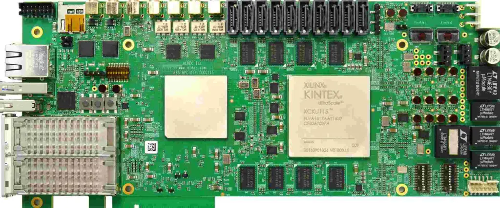
A: The KU115 containing 112 GTH transceivers provides the highest IO capability with up to 3.2Tbps of bandwidth.
Q: What design tools are used for Kintex UltraScale/UltraScale+?
A: Xilinx’s Vivado Design Suite handles FPGA synthesis and implementation for Kintex UltraScale and UltraScale+ devices.
Q: Do all Kintex UltraScale+ families include cost-optimized variants?
A: Yes, cost-reduced versions with fewer transceivers are available in all Kintex UltraScale+ sub-families.