Thinking of getting an FPGA board from Altera? Here’s a list of some of the best FPGA boards available, with various features and purposes. Along with the description, this article includes specifications and ideas of how to get them easily.
Scientists, engineers, and hobbyists use FPGAs for a wide variety of projects. In addition, some people use FPGAs in their daily lives without realizing it. Examples include the following:
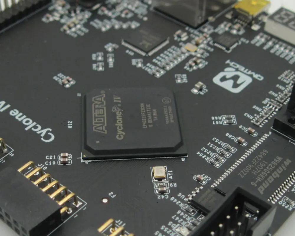
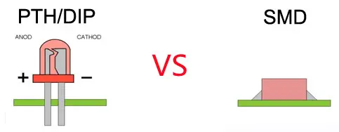
FPGAs are commonly useful in computer-related fields, including image processing, digital signal processing, video compression/decompression, computer vision, data compression/decompression, computer networks, and telecommunication devices developed by manufacturers like RayMing PCB and Assembly.
The Altera series FPGA boards are a multiuser, multi-threaded design suited for many markets such as enterprise automation, digital signal processing, and cyber security. These series include FPGA devices with a comprehensive range of I/O expansion for processor-intensive applications. They include:
Intel Stratix 10 FPGA board:
If you need a compact, powerful FPGA for various engineering applications in various industry sectors, this is your board. FPGA boards are helpful in many different applications, including embedded system design and video processing.
Intel Stratix Ge FPGA board:
This board is specifically designed for the aerospace industry, whereas the Stratix 10 FPGA board is a more general-purpose FPGA. The Ge FPGA board has a bit more computational performance and throughput than the Stratix 10 FPGA board. This board can handle a wide range of applications. The board is also suitable for professional design projects.
Stratix 10 GX FPGA board:
The Ge FPGA board is entirely compatible with the Stratix 10 FPGA board, with extra features and more powerful computing performance. These boards are essential in commercial design projects, especially those involving industrial design or consumer products.
Stratix V FPGA boards:

This is a range of FPGA boards based on the Stratix series. The board offers high-performance and advanced features, such as high-speed transceivers and increased connectivity options. It also has a lower power consumption than previous
FPGA boards that were available from Altera. This can be beneficial in specific applications, such as battery-powered devices. However, its design is also essential for industrial design and engineering applications.
Stratix 7 FPGA board:
This is the latest generation FPGA board based on the Stratix series. The Stratix 7 FPGA board is compatible with the previous models (6, 6 E, 6 GX) and has exclusive features. Like its predecessors, it offers high performance and fast computing capabilities. Like other Altera boards, it comes with excellent software support. As a result, we can use the board in both industrial and embedded design projects.
Arria 10 FPGA board:
If you are looking for a feature-packed high-performance FPGA board and don’t care about the price, this is the FPGA board to consider. So, it offers excellent features at a competitive price. The Arria 10 FPGA board is suitable for use in industrial and commercial design projects.
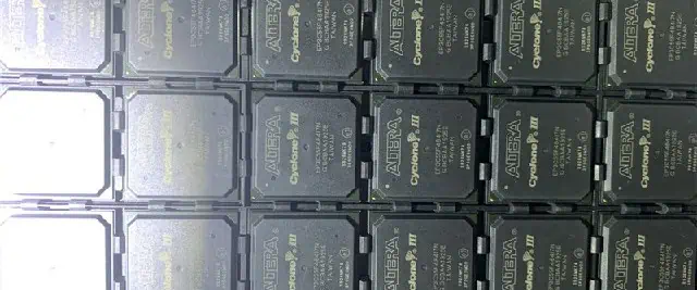
Cyclone III FPGA boards:
These boards primarily target customers who need a high-performance FPGA with fast clock speeds and many I/O pins. We can use the boards in both commercial and industrial design projects. The Cyclone III series design will help to meet the needs of experienced users.
Max V CPLD Boards:
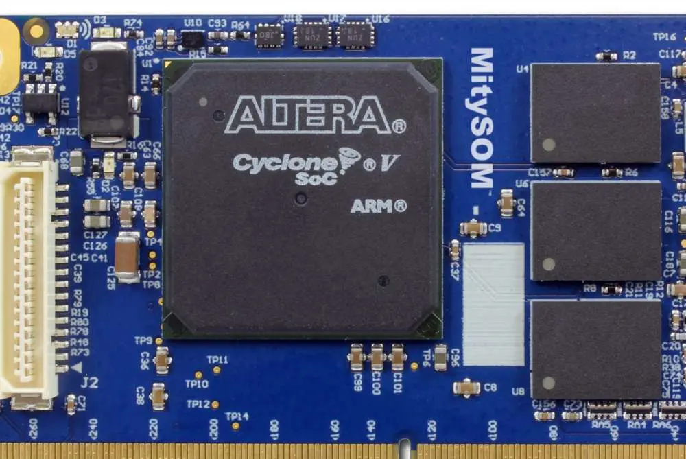
Altera Max V series is a range of programmable logic devices used in various hardware solutions. They are generally used as embedded microcontrollers or for hardware acceleration. The Cyclone V series
FPGA boards also have a wide range of applications, especially in the industrial design and embedded systems sectors.
FPGA development boards:
These boards’ design helps to promote and support application development on FPGAs. They include the Cypress FX2 and Altera Quartus II software for Xilinx and Altera hardware. This lets you interact with the FPGA on your computer and design and build complex systems very quickly.
Stratix 10 SBC:
This is a powerful and compact single-board computer for FPGA design. We can use it as a convenient development platform for hardware debugging and prototyping. It also supports the Altera Quartus II software, which is highly useful for software development on FPGAs.
What is the difference between Xilinx or Altera?
The main difference is that the Xilinx series FPGA boards’ design is mainly for application development. Altera series FPGA boards are essential for industrial design and embedded applications. Because the Xilinx series is more popular, many great tools support Xilinx devices. However, there are differences between the two FPGA brands.
The traditional way of communicating the IP block between devices is Altera’s proprietary communication protocol known as protocol-level interconnect (PLI). Altera’s PLI offers a direct and efficient method of communicating between IP blocks. The Xilinx series FPGA boards use the IEEE 1394 interface, an open, industry-standard protocol supported by all FPGA devices.
Another essential difference is that the Xilinx series FPGA boards have a free software development kit (SDK). Also, it is programmable logic design tools such as Altium Designer and Quartus II. The Altera series FPGA boards do not come with these additional software programs.
Common features of Intel (Altera) series FPGA boards
A custom original design manufacturer (ODM), Intel Corporation, produces Intel’s FPGA boards. The Intel Corporation designs, manufacture, and sells computer hardware and software components.
1. Flip-Flops
They are small blocks of logic that we use to change the state of a signal. Flip-Flops are helpful in digital circuits to hold data bits. The flip-flop design is very common for FPGA boards. On every clock edge, the system copies the input value to the output value. We clock the input value into the flip-flop on the negative edge of the clock. There are two types of flip-flops, namely:
a. D Flip-Flop: The D Flip-Flop copies the data present on its D inputs to its Q outputs on every positive edge of the clock.
d = c
b. T Flip-flop: The T Flip-Flop copies the data present on the positive edges of the clock to its Q outputs. This means that the system only updates the output on every positive edge of the clock. As a result, T-type flip flops are slower than D-type flip flops.
c. B Flip-Flop: The B Flip-Flop copies the data present on its Q outputs to its D inputs on every negative edge of the clock.
d = c
2. Latency
The term latency refers to the time it takes with a signal to reach its final value. Latency reflects the speed of the FPGA board. If latency is too high, you will experience poor performance with your application. We determine the latency by the size of the FPGA block, the clock frequency of the FPGA, and how many Flip-Flops are helpful in each input or output signal. The system divides up the CLK input into several sub-clocks with different frequencies. One of the longest clock frequency dividers determines the latency. The fastest FPGA boards have higher latency. Latency is an essential parameter for an FPGA board to have a fast signal transmission speed.
The Altera series has many improvements over the Xilinx series. So, the Altera series is better than the Xilinx series for applications that need high performance and flexibility. Furthermore, the interface from one block to another is through its advanced proprietary protocols known as protocol-level interconnect (PLI).
3. Multipliers and DSP Slices
Multipliers and DSP slices come in the form of pre-programmed hardware blocks. We can perform the multi-1 operation on an input block. It performs a sequence of logical operations and then copies the result back to the output. As a result, it then clocks the output into an adjacent flip-flop. This results in a fixed delay between feeding the data into the block and when it clocks out. The delays between blocks cause latency in your application.
4. Memory
Memory comes in the form of flash, SRAM, and EEPROM. Flash memory is volatile memory. We can use it to save your configuration settings during an upload. SRAM is non-volatile memory. In SRAM, the data contents remain even when you remove the power from the FPGA board. EEPROM contains read-only memory that can store information in a non-volatile manner when powered up.
5. Clock
The Clock Signal Generator generates all the signals necessary to control the FPGA. An FPGA board has up to 72 clock signals. T=One can distribute these 72 clock signals around the board using 4-bit busing. Different FPGA boards have a different number of clock signals. The number of clock signals is directly proportional to the size of the FPGA block present on the board. This is because larger FPGA blocks need more computational power and thus use more clock signal channels.
6. ADC and DAC
An ADC (analog-to-digital converter) is a device that can convert voltage levels to digital data. A DAC (digital-to-analog converter) works in the opposite direction. So, it converts digital data into analog signals and performs a voltage conversion. For example, if an FPGA board uses an ADC, you could connect it to a pressure sensor and monitor it.
7. DMA
An FPGA board has an on-chip memory called DMA (direct memory access). The capability of this on-chip memory allows the board to transfer blocks of data directly between internal registers and some internal I/O pins. This is useful when you want to control the FPGA board by writing patterns of bytes into its on-chip memory instead of writing whole numbers of bits into its register.
8. Flash
FPGA boards contain flash memory. Flash memory is non-volatile, like EEPROM (electrically erasable programmable read-only memory). However, the read-out process is faster than EEPROM. We use it to store the FPGA configuration file. This file contains all the information that the FPGA needs to execute your design. The number of SPI (serial peripheral interface) interfaces varies amongst different FPGA boards.
Designing FPGAs Into a System
1. Define the system’s requirements
The first step is to define the requirements of your application. You will need to list your application functions, the required capabilities from the FPGA board, and any constraints that you might have with storage or power availability. Write a list of functional blocks for each design requirement. But make sure that you include any additional requirements that might come up later in the design process.
2. System architecture
Design an architecture for your system based on the functional blocks listed in your application requirement document (ARD). Use hardware-description languages to create a block diagram. So, this block diagram is essentially the basis of all FPGA design work. Then, we will use it to program the FPGA board that you choose for your system.
3. Choose an FPGA platform
Once you have completed your block diagram, you will need to choose an FPGA board with the required number of inputs and outputs and support for the clock speeds necessary for your application’s design requirements.
4. Design block diagram
Once you have chosen an FPGA board, you will need to design the functional blocks of your design onto the new FPGA board. Functional blocks are the building blocks of your system. We use them together to complete applications that require complex functions that the individual chips alone do not support.
5. Program new FPGA
Once you have completed designing your new FPGA board, you are ready to program it into the system of your choice using a programming tool for programmers and readers. We use this tool to program FPGA boards for your system.
FPGA Design Tools
1. Traditional FPGA Design Tools:
These tools are useful for simple designs. For example, we use the Spartan-3E FPGA to create a 3D model of a car in a computer graphics package such as Maya or SketchUp. The FPGA chip provides the approximate color information in the software without using an intense GPU or CPU for this task. Modern FPGAs have more flexibility and can perform complex processing in real-time without using these models for programmable logic design.
2. Integrated Design Tools:
The integrated design tool contains the functions for programming the FPGA, placing multiple components into the design, and linking to external components. An example of an integrated design tool that works with Xilinx FPGAs is Vivado Design Suite.
3. Application-Specific Design Tools:
The application-specific design tool allows the user to code directly to the FPGA using a programming language such as C, C++, or Python. A popular integrated design tool explicitly used for FPGAs is Xilinx WebPACK which provides a graphical programming environment and efficient simulation based on open-source tools from the SPIRIT ISE suite.
4. Application-Specific Application-Specific Tools:
These tools create a specific application for a particular FPGA. In the past, People used application-specific tools in conjunction with an integrated design tool. Application-specific tools for FPGAs are becoming much less popular as integrated design tools have greatly improved. However, it is common to use one of these when creating a bitstream in C or C++ using a third-party compiler such as IGLOO2 from Synopsys’ Design Compiler Group.
5. High-Level Synthesis Design Tools:
The high-level design tool allows users to create a bitstream with a high-level language. An application-specific compiler can then compile this language into the corresponding bitstream with the appropriate FPGA or VHDL synthesis tool.
FPGA Applications
FPGA technology has shown great potential in engineering, robotics, search engines, complex data processing, analytics, and many other fields.
The FPGA technology is also used in Smart Grid applications to assist devices with smart sensing capabilities to service or protect the grid. These Grid-scale FPGAs have special features that help detect faults in the grid, which allows for early detection of failure before it becomes serious. In addition, some of these FPGAs contain software libraries and software-defined radio (SDR) modules to allow them to communicate with different types of sensors and hardware.
ERPs or Embedded Real-Time Programmable (ERPs) are small. They also are low-power, versatile microcontrollers designed for high-performance embedded applications. In addition, we can program ERPs in a high-level language such as C or C++, making them useful for many applications.
ERPs have a design that helps to meet the requirements of real-time embedded programming. They are considerably more complex than programmable logic devices. However, ERPs require fewer transistors to implement the same functionality. As a result, they are often useful for applications where timing sensitivity is critical. For instance, high-frequency signal processing, voice recognition/transcription, speech synthesis/recognition, data-acquisition systems, or clock synchronization.
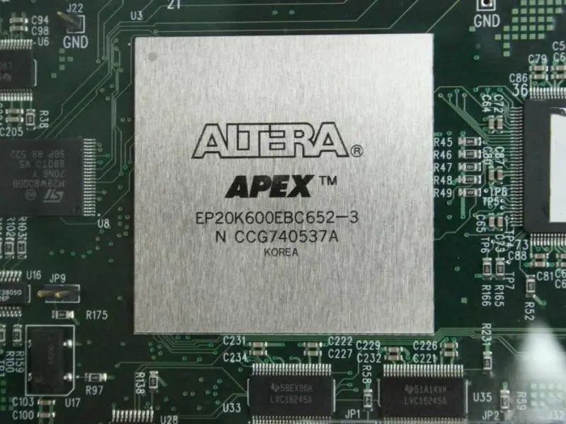
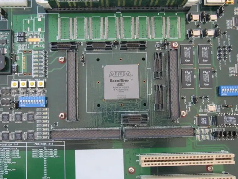
Intel (Altera) series FPGA boards
The Intel (Altera) Cyclone II FPGA Boards
Intel Cyclone II FPGAs are 64-bit ARM Cortex A5-based FPGA modules. As a result, they have low power consumption, high integration with the core of the SoC, and easy configuration by a system-on-chip (SOC) Design Tool. Furthermore, because Intel’s FPGAs use a very efficient Xilinx FPGA fabric, they deliver excellent performance. Additionally, they also deliver density with a very small chip area footprint. The Intel Cyclone II FPGAs are available in various package options. Moreover, they include low-cost fine-pitch BGA–168, fine pitch FBGA–324, and more rugged high-speed QFN packages.
Common specifications include:
- Made In Japan
- RoHS compliance
- Tested all I/O
- One User LED
- Credit-Card-Size 3.386″x 2.126″ (86 x 54 mm)
- High-quality four layers PCB. (Immersion gold)
- 3.3 V single power supply operation with on-board 1.2 V regulator
- AS mode port ( 10 pin socket) for ByteBlasterII or USB Blaster
- JTAG port (10 pin socket) for ByteBlaster [MV/II] or USB Blaster
- Power-on Reset IC
- Directly connected pin header interface for serial communication (TTL)
- SRAM (Cypress CY62256V)
- Two Status LED (Power, Done)
- One User Push-Button Switch
- 30 MHz Oscillator (50 ppm) or External
- Separable VCCIO
- 100 I/O PAD 100 mil (2.54 mm) grid
- SERIAL-FLASH-ROM (M25P40)
- Configuration Device (Altera EPCS4SI8N)
Examples:
Altera EP2C8Q208C8N (Cyclone II FPGA 8K LE)
165,888 RAM Bits, 36 M4K RAM blocks, 100 Maximum user I/O pins (Board), 138 Maximum user I/O pins (Device), 2 PLLs, and 8256 Logic Elements
2. [ACM-201] Altera Cyclone II F672 FPGA board
Altera EP2C35F672C8N
35 Multipliers, 483,840 RAM bits, 105 M4K RAM blocks, 296 Maximum user I/O pins (Board), 475 Maximum user I/O pins (Device), 4 PLLs, and 33216 Logic Elements
Intel (Altera) Cyclone FPGA Boards
The Cyclone FPGA family’s optimization is for high-performance applications that require complex logic functions. It consists of several different FPGA families with varying levels of integration, performance, and features.
Examples:
1. [ACM-004] Altera Cyclone T144 FPGA board
Altera EP1C6T144C8N (Cyclone FPGA 6K LE)
8 Global Clock Networks, 90 Block RAM Bits, 20 M4K RAM blocks, 92 Maximum user I/O pins (Board), 98 Maximum user I/O pins (Device), 2 PLLs, and 5980 Logic Elements
2. [ACM-006] Altera Cyclone Q240 FPGA board
Altera EP1C12Q240C8N (Cyclone FPGA 12K LE)239,616 RAM Bits
52 M4K RAM blocks, 100 Maximum user I/O pins (Board), 173 Maximum user I/O pins (Device), 2 PLLs, and 12060 Logic Elements
Altera EP1C6Q240C8N (Cyclone FPGA 6K LE)
5980 Logic Elements, 2 PLLs, 185 Maximum user I/O pins (Device), 100 Maximum user I/O pins (Board), 20 M4K RAM blocks, and 92,160 RAM Bits
3. [ACM-012] Altera Cyclone Q240 FPGA board (5 V I/O)
EP1C12Q240C8N
239,616 Total RAM Bits, 52 M4K RAM blocks, 100 Maximum user I/O pins (Board), 173 Maximum user I/O pins (Device), 2 PLLs, and 12060 Logic Elements
EP1C6Q240C8N
92,160 Total RAM Bits, 20 M4K RAM blocks, 100 Maximum user I/O pins (Board), 185 Maximum user I/O pins (Device), 2 PLLs, and 5980 Logic Elements
Intel (Altera) Max II CPLD Boards
The MAX 10 and MAX II families of CPLDs offer low power and high performance. The MAX II family’s optimization for applications requires implementing large amounts of logic in a small area.
Examples:
1. [AP68-01] Altera MAX II PLCC68 CPLD Module
EPM570F100C5N
50 Maximum user I/O pins (Board), 160 Maximum user I/O pins (Device), and 570 Logic Elements
EPM240F100C5N
240 Logic Elements, 80 Maximum user I/O pins (Device), and 50 Maximum user I/O pins (Board)
2. [ACM-001] Altera MAXII T144 CPLD board
Altera EPM1270T144C5N (MAXII CPLD 1270 macro cel)
1270 Logic Elements, 116 Maximum user I/O pins (Device), and 100 Maximum user I/O pins (Board)
3. [ACM-005] Altera MAXII T100 CPLD board
Altera EPM240T100C5N (MAXII CPLD 240 macro cel)
80 Maximum user I/O pins (Board), 80 Maximum user I/O pins (Device), and 240 Logic Elements
4. [ACM-302] Altera MAXII T144 CPLD board
Altera EPM1270T144C5N (MAXII CPLD 1270 macro cel)
56 Maximum user I/O pins (Board), 116 Maximum user I/O pins (Device), and 1270 Logic Elements
Intel (Altera) Max V CPLD Boards
The MAX V family of CPLDs offers low power and high performance. These V series has an optimization for applications that require small modules with a more significant number of logic gates or higher density.
Examples:
1. [AP68-02] Altera MAX V PLCC68 CPLD Module
Altera 5M570ZF256C5N
50 Maximum user I/O pins (Board), 159 Maximum user I/O pins (Device), and 570 Logic Elements
Conclusion
The main purpose of an FPGA is to reduce time and money spent on hardware design and faster deployment of new technologies. FPGAs are useful in creating custom hardware solutions for system designers. We can use them as a building block for complex systems with many different applications.
FPGAs contain highly configurable logic blocks connected to perform complex functions. Therefore, one cannot build functions from simple chips alone or combinations of standard chips and microcontrollers (using an embedded controller).