What is an NFC Antenna? A Comprehensive Guide

NFC Antenna

Near Field Communication (NFC) has become an integral part of our daily lives, powering contactless payments, smart access control systems, and seamless device pairing. At the heart of this technology lies the NFC antenna, a crucial component that enables the magic of short-range wireless communication. In this comprehensive guide, we’ll delve into the world of NFC antennas, exploring their function, design, and applications.

1. What is an NFC Antenna?

An NFC antenna is a specialized type of antenna designed to transmit and receive electromagnetic signals in the near-field region, typically within a range of a few centimeters. These antennas are fundamental components of NFC-enabled devices, facilitating the exchange of data between two devices in close proximity.

Key Characteristics of NFC Antennas:

  • Short-Range Operation: NFC antennas are optimized for communication over distances of up to 10 cm, with typical operational ranges of 4-5 cm.
  • Low Power Consumption: Due to their short-range nature, NFC antennas require minimal power to operate effectively.
  • High Frequency: NFC antennas operate at a frequency of 13.56 MHz, which falls within the High Frequency (HF) band.
  • Compact Size: NFC antennas are typically small and can be easily integrated into various devices and form factors.
YouTube video

2. NFC Technology Overview

Before diving deeper into NFC antennas, it’s essential to understand the technology they support. Near Field Communication is a short-range wireless technology that enables two devices to exchange data when brought into close proximity.

Key Aspects of NFC Technology:

  • Standards: NFC is based on RFID standards and is governed by ISO/IEC 14443, ISO/IEC 18000-3, and the NFC Forum specifications.
  • Operating Modes: NFC supports three main operating modes:
    1. Reader/Writer mode
    2. Peer-to-Peer mode
    3. Card Emulation mode
  • Data Exchange Format: NFC uses the NFC Data Exchange Format (NDEF) for storing and exchanging data.
  • Security: NFC incorporates various security measures, including encryption and secure element integration.

Learn More about:

3. NFC Antenna Operating Principles

flexible nfc antenna

Understanding how NFC antennas work is crucial for appreciating their role in NFC technology. These antennas operate based on the principle of electromagnetic induction.

How NFC Antennas Work:

  1. Magnetic Field Generation: When an electric current passes through the NFC antenna, it generates a magnetic field around it.
  2. Inductive Coupling: When two NFC-enabled devices are brought close together, their antennas form an inductive coupling.
  3. Power Transfer: The magnetic field generated by the active device induces a current in the passive device’s antenna, powering it up.
  4. Data Modulation: Data is transmitted by modulating the magnetic field, typically using amplitude shift keying (ASK).
  5. Signal Detection: The receiving antenna detects these modulations and converts them back into digital data.

Near-Field vs. Far-Field Communication:

NFC antennas operate in the near-field region, which is characterized by:

  • Magnetic Coupling: Primarily magnetic field interaction rather than electromagnetic wave propagation.
  • Rapid Field Strength Decay: The field strength decreases rapidly with distance (1/rยณ), limiting the communication range.
  • Non-Radiative: Energy is not radiated into free space, enhancing security and reducing interference.

4. NFC Antenna Design Tips

nfc coil antenna

Designing an effective NFC antenna requires careful consideration of various factors. Here are some key tips for NFC antenna design:

Antenna Geometry:

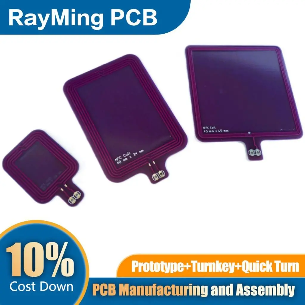
  • Coil Design: Most NFC antennas are designed as planar coils, either circular or rectangular.
  • Number of Turns: The number of turns in the coil affects the inductance and coupling efficiency.
  • Track Width and Spacing: Optimize these parameters for the desired inductance and quality factor.

Material Selection:

  • Substrate Material: Choose a substrate with low dielectric loss for better performance.
  • Conductor Material: Copper is commonly used due to its excellent conductivity and cost-effectiveness.

Impedance Matching:

  • Resonant Frequency: Design the antenna to resonate at 13.56 MHz for optimal performance.
  • Matching Network: Implement a matching network to ensure efficient power transfer.

Size Constraints:

  • Miniaturization Techniques: Use techniques like multi-layer designs or ferrite materials for size reduction.
  • Form Factor Considerations: Adapt the antenna design to fit the intended device or application.

Simulation and Optimization:

  • Electromagnetic Simulation: Use EM simulation tools to analyze and optimize antenna performance.
  • Iterative Design: Refine the design through multiple iterations based on simulation results and prototype testing.

5. NFC Antenna Performance Factors

Several factors influence the performance of NFC antennas. Understanding these can help in optimizing antenna design and troubleshooting issues.

Key Performance Factors:

  1. Quality Factor (Q): A higher Q factor indicates better energy storage and lower losses.
  2. Inductance: The antenna’s inductance affects its resonant frequency and coupling efficiency.
  3. Resistance: Lower resistance leads to better power transfer and read range.
  4. Capacitance: Proper capacitance is crucial for tuning the antenna to the correct resonant frequency.

Environmental Influences:

  • Metal Proximity: Nearby metal objects can detune the antenna and reduce performance.
  • Electromagnetic Interference: External EM fields can interfere with NFC communication.
  • Temperature Variations: Extreme temperatures can affect antenna performance and durability.

Performance Optimization Techniques:

  • Ferrite Shielding: Use ferrite materials to shield the antenna from metal surfaces and improve performance.
  • Adaptive Tuning: Implement dynamic tuning circuits to compensate for environmental changes.
  • Multi-Antenna Systems: Use multiple antennas for improved coverage and reliability in challenging environments.

6. Main Types of NFC Antennas

long range nfc antenna

NFC antennas come in various types, each suited for different applications and form factors. Understanding these types can help in selecting the right antenna for a specific use case.

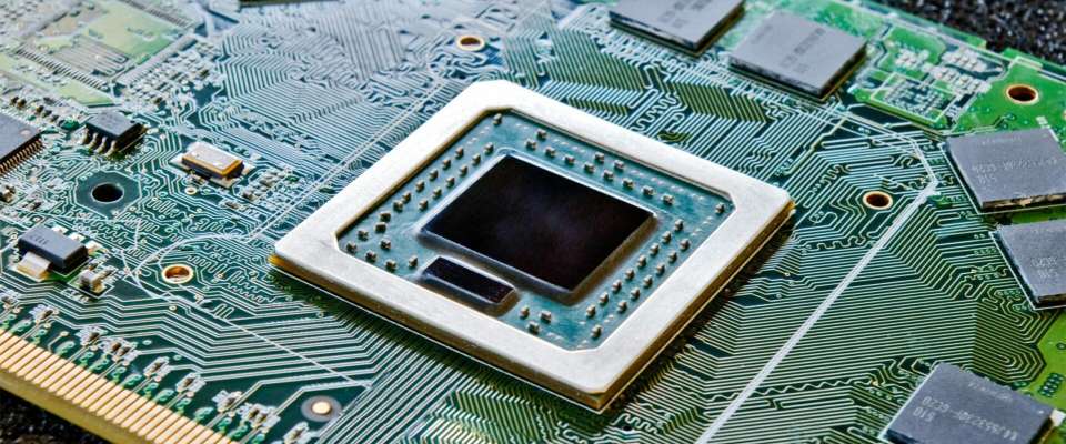
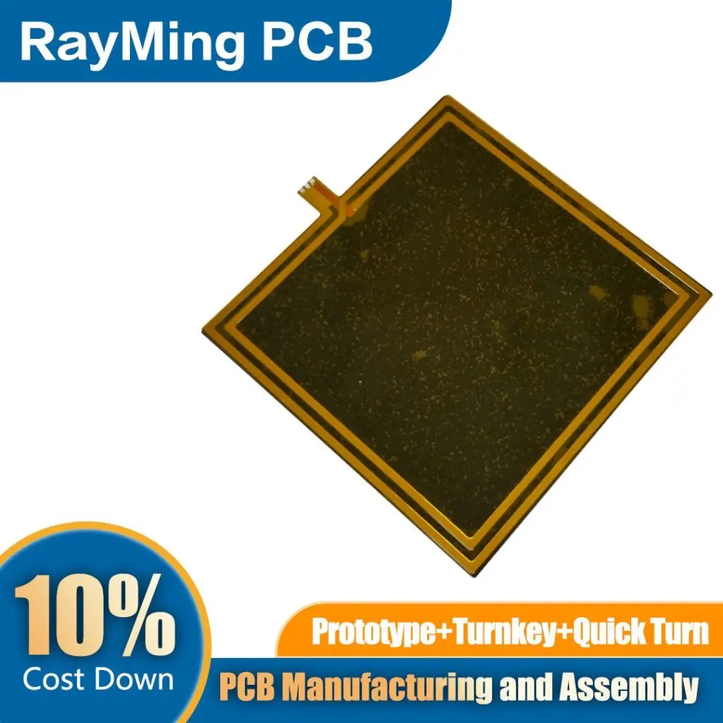
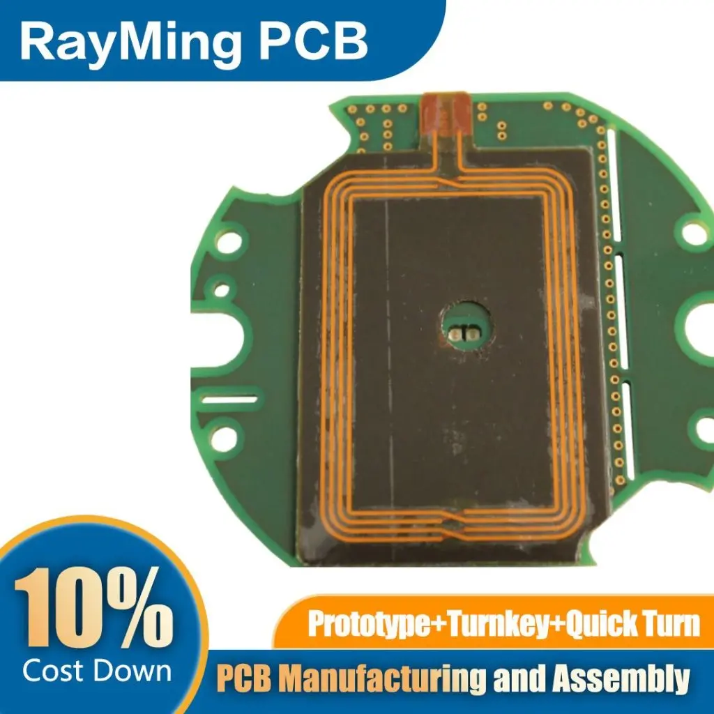
1. Printed Circuit Board (PCB) Antennas:

  • Description: Etched or printed directly on the PCB.
  • Advantages: Cost-effective, easy to manufacture, good for mass production.
  • Applications: Smartphones, tablets, payment terminals.

2. Flexible Printed Circuit (FPC) Antennas:

  • Description: Printed on flexible substrates like polyimide.
  • Advantages: Thin, flexible, can conform to curved surfaces.
  • Applications: Wearables, smart cards, flexible electronics.

3. Ferrite Sheet Antennas:

  • Description: Coil antenna mounted on a ferrite sheet.
  • Advantages: Improved performance near metal surfaces, smaller size.
  • Applications: Devices with metal casings, automotive applications.

4. Air-Core Coil Antennas:

  • Description: Wire wound into a coil without a core.
  • Advantages: Simple design, low cost, good for large-area coverage.
  • Applications: RFID readers, access control systems.

5. Ceramic Antennas:

  • Description: Antenna elements embedded in a ceramic substrate.
  • Advantages: High Q factor, good temperature stability, small size.
  • Applications: High-performance NFC devices, industrial applications.

7. NFC Antenna Integration

Integrating NFC antennas into devices requires careful consideration of various factors to ensure optimal performance and reliability.

Integration Challenges:

  1. Space Constraints: Fitting the antenna into small or thin devices.
  2. Interference: Managing interference from other components and nearby metal objects.
  3. Performance Optimization: Ensuring consistent performance across different device configurations.

Integration Best Practices:

  • Antenna Placement: Position the antenna away from sources of interference and metal components.
  • Shielding: Use appropriate shielding techniques to isolate the antenna from other electronic components.
  • Matching Network Design: Carefully design the matching network to optimize power transfer and bandwidth.
  • Thermal Management: Consider the thermal impact of nearby components on antenna performance.

Device-Specific Considerations:

  • Smartphones: Balance antenna performance with other antennas (e.g., Wi-Fi, cellular) and internal components.
  • Wearables: Design for flexibility and durability in wearable form factors.
  • IoT Devices: Optimize for low power consumption and long-term reliability.
  • Payment Terminals: Ensure consistent performance across various card types and usage scenarios.

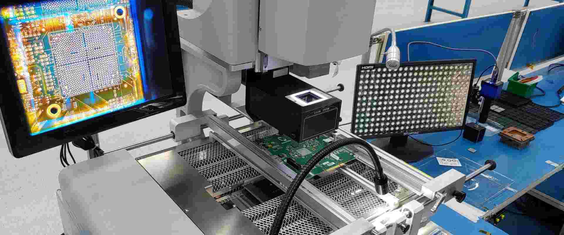
8. NFC Antenna Testing

Thorough testing is crucial to ensure NFC antennas meet performance specifications and regulatory requirements.

Key Testing Parameters:

  1. Resonant Frequency: Verify that the antenna resonates at 13.56 MHz.
  2. Bandwidth: Measure the antenna’s bandwidth to ensure it covers the required frequency range.
  3. Impedance Matching: Check the antenna’s impedance match to the NFC chip.
  4. Quality Factor (Q): Measure the Q factor to assess the antenna’s efficiency.
  5. Read Range: Test the maximum distance at which reliable communication can be achieved.

Testing Methods:

  • Network Analyzer Measurements: Use a vector network analyzer to measure S-parameters and impedance.
  • Field Strength Measurements: Measure the magnetic field strength at various distances from the antenna.
  • Functional Testing: Perform real-world tests with various NFC tags and devices.
  • Environmental Testing: Subject the antenna to temperature, humidity, and mechanical stress tests.

Regulatory Compliance:

  • EMC Testing: Ensure the antenna meets electromagnetic compatibility standards.
  • SAR Testing: For body-worn devices, verify compliance with Specific Absorption Rate (SAR) limits.
  • Certification: Obtain necessary certifications from bodies like the NFC Forum and regulatory agencies.

9. NFC Antenna Applications

nfc reader antenna

NFC antennas enable a wide range of applications across various industries. Here are some key areas where NFC technology is making a significant impact:

1. Contactless Payments:

  • Mobile Wallets: NFC-enabled smartphones for tap-to-pay transactions.
  • Contactless Cards: Credit and debit cards with embedded NFC antennas.
  • Wearable Payments: NFC-enabled watches, rings, and other wearables for payments.

2. Access Control:

  • Smart Locks: NFC-based door locks for homes and offices.
  • Public Transportation: Contactless ticketing systems for buses, trains, and metros.
  • Event Ticketing: NFC tickets for concerts, sports events, and conferences.

3. Device Pairing and Data Transfer:

  • Bluetooth Pairing: Quick pairing of Bluetooth devices using NFC.
  • Wi-Fi Configuration: Easy Wi-Fi setup for IoT devices.
  • Contact Information Sharing: Business card exchange using NFC-enabled devices.

4. Product Authentication:

  • Anti-Counterfeiting: NFC tags for verifying the authenticity of luxury goods.
  • Supply Chain Management: Tracking and authenticating products throughout the supply chain.
  • Wine and Spirit Verification: NFC-enabled bottle caps for confirming product genuineness.

5. Healthcare:

  • Patient Identification: NFC wristbands for quick and accurate patient ID.
  • Medication Tracking: NFC-enabled pill bottles for medication adherence monitoring.
  • Medical Device Pairing: Simplified pairing of medical devices with monitoring systems.

6. Automotive:

  • Keyless Entry: NFC-based car keys for unlocking and starting vehicles.
  • In-Vehicle Payments: NFC-enabled systems for toll payments and fueling.
  • Personalized Settings: Automatic adjustment of car settings based on the user’s NFC device.

7. Gaming and Entertainment:

  • NFC-Enabled Toys: Interactive toys that respond to NFC tags.
  • Gaming Accessories: NFC-based character figurines for video games.
  • Content Sharing: Sharing game progress or media content between devices.

8. Smart Home:

  • Device Control: NFC tags for triggering smart home routines.
  • User Identification: Personalized settings based on NFC device detection.
  • Guest Access: Temporary NFC-based access for visitors.

10. The Future of NFC Antennas

As NFC technology continues to evolve, so too will the design and capabilities of NFC antennas. Here’s a look at some trends and potential future developments in NFC antenna technology:

Miniaturization and Integration:

  • Nano-Scale Antennas: Development of extremely small NFC antennas for integration into tiny devices.
  • Flexible and Stretchable Antennas: Advancements in materials science enabling highly flexible and conformable NFC antennas.
  • Integrated Circuit Antennas: Direct integration of antennas into NFC chip packages for ultra-compact designs.

Performance Enhancements:

  • Extended Range: Research into increasing the effective range of NFC communication while maintaining security.
  • Multi-Protocol Support: Antennas capable of supporting multiple wireless protocols (e.g., NFC, Bluetooth, UWB) simultaneously.
  • Energy Harvesting: NFC antennas that can harvest energy from ambient RF signals to power small devices.

Advanced Materials:

  • Metamaterials: Use of engineered materials with unique electromagnetic properties for enhanced antenna performance.
  • Graphene-Based Antennas: Exploration of graphene and other 2D materials for ultra-thin, high-performance antennas.
  • Self-Healing Materials: Development of antennas that can repair minor damage autonomously.

Smart Antennas:

  • Adaptive Tuning: Antennas with built-in intelligence to dynamically adapt to changing environments.
  • Beamforming: Implementation of beamforming techniques to improve directionality and range.
  • Cognitive Antennas: Antennas that can learn and optimize their performance based on usage patterns.

Enhanced Security:

  • Quantum-Resistant Designs: Development of NFC antennas and protocols resistant to quantum computing attacks.
  • Biometric Integration: Combination of NFC technology with biometric authentication for enhanced security.
  • Physical Unclonable Functions (PUFs): Integration of PUFs into NFC antennas for unique device identification.

Emerging Applications:

  • Human-Machine Interfaces: NFC antennas as part of advanced user interface technologies.
  • Biomedical Implants: Ultra-small, biocompatible NFC antennas for medical implants and sensors.
  • Environmental Monitoring: Widespread deployment of NFC-enabled sensors for environmental and infrastructure monitoring.

Standardization and Interoperability:

  • Global Standards: Development of unified global standards for NFC antenna design and performance.
  • Cross-Technology Integration: Seamless integration of NFC with other wireless technologies for enhanced functionality.
  • Open Ecosystems: Creation of open platforms for NFC antenna design and application development.

As these advancements unfold, NFC antennas will continue to play a crucial role in enabling seamless, secure, and intuitive interactions between devices and the physical world. The future of NFC antenna technology promises to bring us closer to a truly interconnected and smart environment, where the boundaries between digital and physical realms become increasingly blurred.

Conclusion

NFC antennas, though often overlooked, are the unsung heroes of the contactless communication revolution. From enabling secure payments to facilitating seamless device interactions, these compact components have become integral to our digital lives. As technology continues to evolve, NFC antennas will undoubtedly play an even more significant role in shaping our connected future.

Understanding the principles, design considerations, and applications of NFC antennas is crucial for engineers, product designers, and technology enthusiasts alike. By harnessing the power of these innovative antennas, we can continue to create more intuitive, secure, and efficient ways for devices to interact with each other and with the world around us.

As we look to the future, the potential applications of NFC technology seem boundless. From advanced biomedical implants to smart cities and beyond, NFC antennas will be at the forefront of this technological revolution, silently but powerfully enabling the connections that drive our increasingly digital world.

What is the Metal Core PCB Difference Between Aluminum PCB and Copper Base PCB?

Aluminum PCB VS. Copper Base PCB

What is the difference between Copper base PCB and Aluminum base PCB? MCPCB has a metal base with superior thermal conductivity and better heat dissipation. You can find both types of PCBs in any electronics store. Learn what makes them different and choose the best material for your project.

What is Aluminum PCB?

Before determining what an aluminum PCB is, we need to understand its main characteristics. These include Thermal conductivity, Dielectric layer, Electrical insulation, and flexibility. The following sections explain these qualities in greater detail. Read on to learn about the advantages of this material! Also, read about the benefits of insulating a PCB with aluminum.

Thermal conductivity

The thermal conductivity of aluminum PCBs varies according to the copper layer in the circuit. Different processes will result in different levels of thermal conductivity. Aluminum has poorer thermal conductivity than PCB board. Thermal conductivity also depends on the aluminum substrate and pad design. Copper foil and aluminum plates are typically laminated together to create a single board. The thermal conductivity of aluminum PCBs can vary remarkably. The following are some characteristics to consider when selecting an aluminum-based PCB:

Aluminum PCB Applications

The thermal conductivity of aluminum PCB is higher than that of copper. However, it is still not as high as copper. This is because aluminum is thinner than copper, and copper is much denser. Therefore, a thicker aluminum PCB will be more resistant to heat, while a thin aluminum one will have less resistance. These properties will reduce breakdown voltage, so aluminum PCBs should help low-voltage applications.

Aluminum PCBs have excellent electrical insulation and thermal conductivity. This means they can carry more current than other materials, including FR-4. In addition, because of their thermal conductivity, they can withstand higher temperatures than other materials. The thermal conductivity of aluminum PCBs enables Rayming PCB & Assembly to make more efficient electronic circuits. Moreover, aluminum PCBs can be more durable than FR-4, prone to damage.

Aluminum PCBs are often helpful in lighting and electrical devices. To extend its lifespan, make sure to store them in a dry, dark place. They can yellow or blacken due to moisture. The best way to store aluminum PCBs is to use them within 48 hours after removing them from their vacuum packaging. If you are unsure of what to do with your aluminum PCBs, consult with an experienced electrical engineer.

Dielectric layer

An aluminum PCB has an interior dielectric layer composed of a ceramic or thermally conductive material. A thermally conductive dielectric layer helps manage the heat in a project while keeping the temperature within specified limits. Typical thicknesses of dielectric layers range from 0.05 to 0.2 mm. In addition to the dielectric layer, an aluminum membrane layer protects the aluminum core and is crucial for the proper function of the IC.

A dielectric layer consists of copper or aluminum foil. Its thickness varies depending on the requirements. Copper-clad laminates generally have a copper base layer that is 50mm thick. The metal base layer is also thermally conductive. The aluminum base layer has high thermal conductivity and a copper foil layer that is 50 to 200mm thick.

An aluminum PCB with an insulating dielectric layer is excellent for several applications. These PCBs offer dimensional stability and are suitable for power device surface mount technology. Additionally, aluminum PCBs reduce the overall volume of the product. They also exhibit superior reliability. They can also help prolong the shelf life and increase its power density. And since aluminum is cheap, this material makes it a good choice for manufacturing power electronics products.

Electrical insulation

The insulating layer consists of electrolytic copper foil with a thickness of one to ten ounces. A ceramic polymer serves as a critical module of a PCB and has excellent thermal and viscoelastic properties. Therefore, copper foils, anywhere from one to ten ounces in weight, are in the insulating layer.

An aluminum PCB’s high-voltage test ensures its complete electrical insulation. It must pass a high voltage test that measures 100 percent of the printed board’s surface area. When a PCB fails a high voltage test, it will likely experience leakage, fire, or malfunction. Delamination and blistering of the aluminum base are defects in an aluminum PCB. As a result, you should ensure that your aluminum PCB passes these tests.

Metals are highly conductive, so it’s essential to protect your PCB from accidental conductivity. While it is a good conductor of heat, it also conducts electricity. In some situations, metal substrates are necessary because they can handle powerful electrical currents. However, this doesn’t mean that a PCB without any insulation will fail, even if it’s just slightly conductive. Ultimately, it’s essential to match the electrical insulation on your PCB with the environment in which you intend to use it.

In addition to aluminum PCBs, copper PCBs are another way to make thermally-efficient circuits. Copper-based PCBs work as a central core of a complex thermal structure. Still, aluminum is also an excellent choice for this application because it can provide outstanding electrical insulation and excellent thermal conductivity. The aluminum PCB’s copper-based circuit layers consist of a metal-based copper-clad laminate and excellent electrical insulation.

Flexibility

The process for manufacturing flexible aluminum PCB includes multiple thermally conductive dielectric materials. They connect to the circuitry layers using signal and thermal vias. They are also composed of ceramic filters and polyimide resin. This material provides high flexibility and remarkable thermal efficiency.

The flexibility of aluminum PCBs allows them to bend during installation. They are available in single, double, and multi-layer layouts. They are used to replace bulky wiring with superior gear. Flexible aluminum PCBs are also available with higher thermal performance.

The flexibility of aluminum PCB depends on its construction and conductive layers. It also depends on plated through holes for connection. The more flexible aluminum PCBs you order, the more money you’ll save. It’s also a great option if you have space constraints. If you have limited space, flexibility is essential for your device. It’s worth the extra cost. And it’s also a good option for many applications.

Applications

The use of aluminum PCBs has several benefits for circuit designers. Due to its increased thermal conductivity, it provides better electrical insulation. Its thin-film dielectric layer also helps to remove heat from the circuit. Copper foil is one of the primary components of aluminum PCB. Using this material is an environmentally friendly choice but requires proper expertise in the manufacturing process.

Another benefit of aluminum PCBs is that they are less susceptible to damage from moisture and heat. In the case of a cooling system, it can replace a ceramic substrate or a radiator component. Aluminum PCBs can also help in automobiles, audio equipment, and power supply devices. The power supply applications include switching regulators, DC/AC converters, and high-frequency amplifiers.

In addition to the advantages of aluminum PCB, it is also lightweight and low-cost. We can make it into various shapes and thicknesses according to the user’s needs. There are several types of aluminum PCB: through-hole, flexible, and multi-layer. They have their advantages and disadvantages. You should consider the pros and cons of aluminum PCBs before deciding.

What is Copper Base PCB?

Copper Base PCB

You may be wondering: What is copper base PCB? A PCB is an electronic circuit board containing copper as one of its constituent elements. There are different PCBs, and they all have their benefits and drawbacks. For this article, I will compare copper-based PCB and MCPCB. You’ll need to know the basic differences between the two types to do this.

MCPCB

The basic design of an MCPCB consists of a copper core, a thermal insulating layer, IC components, and a solder mask. This design is also a COB MCPCB or “Chip-On-Board” PCB. Copper is more expensive than aluminum, unlike aluminum PCB, making it an economical option for some applications.

MCPCBs have many advantages over other PCB types. First, MCPCBs does not require vias for thermal relief, which makes them ideal for high-heat applications. Second, MCPCBs require much less drilling than other PCBs, which only need a few large holes to mount components. Finally, these are also known to be more durable and withstand repeated mechanical shocks and thermal cycles.

Another advantage of MCPCB is that it allows for better etching. For example, we can etch Copper-based PCBs into a boss shape, which is excellent for pasting components. In addition, copper has a different modulus of elasticity than aluminum, making them more stable than aluminum PCBs. This is an essential advantage when comparing copper-based vs. aluminum-based PCBs.

MCPCBs are also cheaper than FR4 and aluminum-based PCBs. However, they require a higher level of precision and cost. Aluminum-based PCBs are less expensive than copper-based PCBs and are generally helpful in areas with high requirements. On the other hand, a copper-based PCB can handle temperatures as high as 450 degrees Fahrenheit.

Copper base PCB

If you’re planning to use a copper base PCB in your electronic device, it’s essential to know more about it before you order it. The term “copper base” can refer to any electronic board. While “copper” may not be the most familiar, it is an excellent option for electronic circuit boards.

Unlike the usual single-sided PCB, double-sided metal-core PCBs use a metal core between two conductors layers. The copper layer sits between the two conductor layers, with the metal core connected to the conductors through vias. Unlike the other two types, a copper-core PCB can withstand high temperatures.

Copper-based PCBs are the most expensive type of metal core PCB. They are also more expensive than their aluminum and iron-based counterparts. However, they perform better in heat conduction and thermal diffusivity and are ideal for high-frequency circuit design, high-heat-dissipation circuits, and high-precision communication equipment.

A copper-based PCB is also commonly known as an MCPCB. It’s a printed circuit board with a metal core and insulation layer. It has superior heat-dispersing properties and superior mechanical strength. Aluminum-based PCBs are more cost-effective than copper-based ones. Copper-based PCBs are often used in electronic communication equipment and LED lighting, among other things.

Compared to aluminum, copper has a higher conductivity rating than aluminum. In addition, its density makes it ideal for multiple-layer PCBs. On the other hand, aluminum is an excellent choice for single-layer PCBs but is less efficient for multi-layer PCBs. Besides, aluminum has a much lower carbon footprint than copper. Therefore, if you’re considering copper-based PCBs for your products, ensure you get a PCB with a heavy copper base.

MCPCB symmetry

We achieve the symmetry of MCPCB multiple set-ups containing a metal core by having similar-thickness layers over and beneath the board’s metal backing. A six-layer board, for example, would have three layers above and below the metal backing. In addition, it is essential to avoid the warpage or MCPCB LEDs. Additionally, plated through-holes are unnecessary because they can lead to electrical shorts and poor performance.

The copper PCB is often embedded with other circuitry to improve performance and reliability. For example, electronic device manufacturers use MCPCBs with copper cores. The copper track between components makes it possible to fit the PCB in a small device. This type of PCB is more expensive than those with aluminum cores, but they are also stronger and more reliable.

The metal base layer helps dissipate heat and enables the copper foil to create the desired pattern. Copper base PCBs are the most expensive type of MCPCB and use copper substrate core technology. Therefore, the copper base PCB is the costliest type of MCPCB, but it has the highest thermal conductivity.

To design an MCPCB, you must know how copper conducts electricity and heat. To achieve this, you must have a high-density copper foil at least 35mm thick. Copper foil with low conductivity will cause a short and will have to be isolated from the copper base.

While a metal core PCB has a metal core and insulation layer, the metal base PCB is not much different from a CEM3 or FR4 board. However, it has a metal copper film core in the middle or on the back, which can divert heat away from the heat-sensitive parts of the PCB. It also has better processing capabilities compared to other types of PCB.

Aluminum PCB VS Copper base PCB

What is the difference between an Aluminum PCB and a Metal Core PCB? A PCB made with a Metal Core is a higher quality version. For this type of PCB, the main substrate board consists of a Metal Core. It also contains a copper layer. However, unlike an Aluminum PCB, a Metal Core PCB does not receive any surface finish or solder mask.

Copper printed circuit boards are used in high-power rectifiers and pumping plants to ensure high power. Their superior electrical and thermal conductivity makes them suitable for the smallest electronic devices. While copper printed circuit boards have many advantages over aluminum, they still need a copper base for a few important reasons. Copper PCBs are also more expensive than aluminum and iron PCBs.

Prototyping a Metal Core PCB is like prototyping and Aluminum PCB. The basic process of prototyping starts with a design software suit. When you decide to use a PCB manufacturer, you should know the software they use for prototyping. Metal Core PCB manufacturers should also know which software they use for prototyping.

The difference between Copper and Aluminum PCBs is most evident in how copper has higher thermal conductivity and is, therefore, more suitable for single-layer PCBs. On the other hand, aluminum is much more difficult to manufacture for multiple-layer PCBs. Therefore, copper is the ideal metal for multiple layers. In addition to being lighter, aluminum is also better for environmentally friendly reasons.

MCPCB has a metal base

The term “Metal Core PCB” refers to the base material. The main substrate board is composed of a metal core. A metal mask is applied to the board before the soldering process begins. The solder mask includes a copper base and black and clear printed circuit boards.

A prototype of a metal core printed circuit board is a lot like a typical PCB. It requires a metal base and must adhere to certain guidelines. The final figure of the circuit board should resemble the design. Different design software is ideal for this purpose. For example, OrCAD, Altium Designer, KiCAD, Eagle, and KiCAD are popular choices. Once the design is complete, designers export schematics to the PCB manufacturer. Gerber is an essential tool for forwarding schematics because it preserves the aesthetic appeal of the PCB.

The base of a Metal Core PCB serves as a heat sink, transferring heat away from critical components. Different metals can be the base of a PCB. Aluminum is the most common, but copper is the best for performance, although it is also the most expensive. The base is typically 1 to 4 mm thick, depending on the customer’s requirements. This layer is often the first layer of a PCB.

Metal Core PCBs are ideal for high-temperature applications, such as amplifiers and solid-state relays. Because metal is thermally conductive, it helps dissipate heat efficiently, ensuring that the device’s life span and performance remain high. In this way, the metal core PCB is perfect for these high-temperature conditions. And unlike the FR-4, the MCPCB can withstand the highest temperatures in the market.

MCPCB has excellent heat dissipation

In electronics, thermal management is an important consideration. Temperatures that exceed the acceptable range can cause physical destruction and system failure. Metalcore PCBs are ideal for applications requiring high thermal dissipation. This type of PCB has several advantages. Its high thermal conductivity, 1.6 mm thickness, and 270 mm2 board size make it a better choice for many applications.

Due to their superior heat dissipation, metal core PCBs are helpful in various applications. They are particularly suited for power electronic devices, such as high-drain-current MOSFETs, switching supply circuits, and LED light circuits. Metalcore PCBs have a basic configuration of conductive layers that facilitate heat dissipation.

The process for producing an MCPCB is like the standard FR4 PCB. The only difference is the material used for the layers. For example, FR4 is a very strong material. Therefore, an MCPCB has excellent heat dissipation properties despite its high density. Moreover, MCPCBs does not require vias, leading to shorts or other problems.

The main applications of Metal Core PCBs include solid-state relays, LED lighting, and motor control in electric vehicles. Metal PCBs are ideal for applications that generate heat. They also perform better than traditional FR-4 substrates for fast cooling. The most used metal layer is aluminum, which is very conductive. Aluminum is also non-toxic, recyclable, and possesses a high thermal conductivity.

It has a better thermal conductivity

There are many advantages to a Metal Core PCB. It is known for its better thermal conductivity, and it can redirect heat away from electronic components. It is one of the best PCB substrates, and its superior thermal conductivity makes it an excellent choice for many electronics. Aluminum is one of the most used metals used for PCBs. Copper and aluminum both offer better thermal conductivity than FR-4.

Metalcore PCBs are helpful in applications that generate enormous heat and cannot be cooled using conventional fans. They are used to achieve high illumination with fewer requirements than traditional LEDs. They are also helpful in military and aerospace applications, which must withstand thermal cycling and repeat mechanical shocks. This makes them the perfect choice for such demanding uses. Furthermore, MCPCBs are more durable than normal PCBs, susceptible to damage due to heat and moisture.

Different manufacturers fabricate their boards differently for Metal Core PCBs. For example, a simple one-layer MCPCB has a copper circuit layer at the top, a thermally conductive dielectric layer underneath, and a metal core base layer. The fabricator then assembles these three layers. The copper and aluminum layers provide an efficient path for heat from electronic components to reach the circuit board.

High-power components produce a large amount of heat, making it necessary to transfer the heat as fast as possible. Hence, metal core PCBs are popular in the power supply and converter industry, LED lighting systems, and automotive systems. In addition, they are better suited to resist heat transfer than FR-4 PCBs, preventing damage to the circuit and components. For these reasons, it is essential to make sure that the PCB you use has an excellent thermal conductivity rating, as this will increase the life of your product.

It has a symmetrical stack-up

When designing a metal core PCB, it is essential to follow several design guidelines. As its name suggests, a metal core is a layer of metal attached to the back of a PCB. Usually, this layer is made of aluminum, although copper and stainless steel are also possible materials.

When designing a metal core PCB, it is essential to avoid plated through holes. As these holes can short circuits, isolating the metal layer from the plated through-hole is essential. A hole in the metal core is drilled 40 to 50 mils larger than the plated through-hole component, filling it with a non-conductive epoxy filler.

The conductive layers in the PCB stack-up are in an alternating pattern, with the top-most conductive layer 102A positioned above the bottom-most prepreg layer 104G. The same applies to the insulating layers. As a result, the stack-up is symmetrical, and the structure of the PCB is also symmetrical.

Buy XA7A15T-1CPG236I Xilinx FPGA From Raypcb

xilinx Spartan-3A AN

Xilinx XA7A15T-1CPG236I is a 2010 Non-RoHS Compliant BALL Field Programmable Gate Array (FPGA). If you are looking to buy an automotive FPGA, this is one of the best out there.

Continue reading to find out more about the features that make Xilinx XA7A15T-1CPG236I one of the best Field Programmable Gate Arrays (FPGAs) out there.

Xilinx XA Artix-7: The Series

It is common to see series of Field Programmable Gate Arrays (FPGAs). These are broad classifications of the circuits and depending on the manufacturer, the functionalities tend to differ.

The Xilinx XA7A15T-1CPG236I belongs to the Xilinx XA Artix-7 series; a family of FPGAs from Xilinx. It is primarily used for automotive designs and just like every board in the series, it spots unique features.

One of the outstanding features is the highest operating standards with the operating temperature being as high as 125-degree Celsius.

Specifications of the Xilinx XA7A15T-1CPG236I FPGA

In this section, we talk about the innovative characteristics or features that make Xilinx XA7A15T-1CPG236I outstanding out of the other FPGAs in the series.

1. Number of Pins

First, let us understand what Pins are in terms of their usage in a Field Programmable Gate Array (FPGA). Pins are one of the primary components of a circuit board chip. They also double as the connection between the peripheral circuits and the internal circuits of the FPGA.

A total of 236 are embedded in the Xilinx XA7A15T-1CPG236I, giving designers more ways to connect the internal and external circuits in the chip.

2. Terminal Specifications

Terminals are also one of the most important attributes of an FPGA. For the Xilinx XA7A15T-1CPG236I, its terminal specifications are discussed below:

Input and Output (I/O)

The Input and Output (I/O) of a Field Programmable Gate Array (FPGA) refers to the medium of processing information within the Integrated Circuit (IC)/chip and the external circuits. The Xilinx XA7A15T-1CPG236I has a total I/O of 106.

Outputs

Just like the Input and Output (I/O), outputs in an Integrated Circuit (IC) are used to establish a connection between the internal and external circuits.

The total number of Outputs in the Xilinx XA7A15T-1CPG236I FPGA are 210. In addition, these Outputs are used to reproduce or display the results being processed and released by an input device into the Integrated Circuit.

Terminations

A termination in an Integrated Circuit (IC) or FPGA refers to the termination or stoppage of a transmission line. For this to happen, the terminations must have been set and triggered.

Also, the triggering of terminations in the chip prevents signals from being reflected at the other end of the transmission line.

Terminal Pitch

Xilinx XA7A15T-1CPG236I has a terminal pitch of 0.5 millimeter. The role of the terminal pitch in an Integrated Circuit (IC) is to serve as the central point of ending the functions of a conductor in the electronic component.

The terminal pitch also has other uses that include establishing connection to the external circuits on the pitch.

Terminal Finish

The terminals in the Xilinx XA7A15T-1CPG236I are completed with the trio of Tin, Silver and Copper. That forms the compilation: Tin/Silver/Copper also interpreted as (Sn/Ag/Cu).

As a rule of thumb, the terminal finish in a chip must not be done with lead. It is best to leave the terminal finish free of lead-finishing because that goes a long way to improve the temperature strength of the chip.

That way, the plastic used in molding the component would be able to withstand the higher temperatures that may be tenable when the board is in use.

Location of the Terminal

The Terminal Position, also known as the โ€œLocation of the Terminal,โ€ refers to the point where the conductor of the electronic component comes to an end.

3. Memory Storage

The memory storage of a Field Programmable Gate Array (FPGA) is interpreted as RAM bits. That is, the Random Access Memory. The RAM bits of the Xilinx XA7A15T-1CPG236I is 921600. This provides enough storage space to safely store the data in the semiconductor.

4. Number of Registers

The total number of registers in the Xilinx XA7A15T-1CPG236I is 20800. For emphasis, the role of a Register in a semiconductor or Integrated Circuit (IC) is to store the binary code. The binary code, in turn, comprises flip-flops that have storage functionalities.

5. Propagation Delay

Propagation Delay refers to the delay or the slight wait before a full propagation or programming of an Integrated Circuit (IC) can be completed. The Propagation Delay in the Xilinx XA7A15T-1CPG236I is 130 ps.

During this wait, the configuration of the data in the internal circuit will be put on hold pending the completion of the propagation.

Also, the Propagation Delay in an Integrated Circuit (IC) can differ by the input. There is a chance that the delays may be extended, especially if the other elements in the chip are the same/constant.

6. Security Features

The security of the Xilinx XA7A15T-1CPG236I is also very paramount. In addition to ensuring that it functions optimally, it is also important to protect it from damage. Here are some of the security attributes of its Integrated Circuit (IC):

Peak Reflow Temperature (Cel)

One of the security features integrated into a Field Programmable Gate Array (FPGA) is the Peak Reflow Temperature. It has to do with the maximum temperature that the electronic components inside the circuit can be exposed to. Anything above that could trigger excessive temperature that would make the components susceptible to damage.

As the Xilinx XA7A15T-1CPG236I is a Surface Mount Technology (SMT)-powered IC, it uses a 260 Peak Reflow Temperature to control the electronic components from damage.

Speed Grade

Speed Grade in an FPGA infers to the pin-to-pin latency. It also refers to how quick the device can work, provided that the cpld is lower.

The Speed Grade of the Xilinx XA7A15T-1CPG236I IC is 1.

RoHS Status

RoHS is a mandatory compliance standard that is used to reduce the excessive usage of harmful components in either electrical or electronic components.

The Xilinx XA7A15T-1CPG236I is Non-RoHS compliant, raising concerns over the conducive use of the chip, as it relates to protecting the environment and reducing risks for human use.

Conclusion

With the Xilinx XA7A15T-1CPG236I in your electronic device, you can be confident of using electronic components that are applicable for automotive uses. The Integrated Circuit (IC) has been in use since 2010. However, you need to be careful with its uses, as it is currently Non-RoHS compliant.

Contact Rayming Technology (RayPCB) to help you design this circuit and fix any other special specifications you want on it.

AMD Xilinx XA7A25T-1CPG238Q FPGA Distributor

Xilinx Spartan-6 FPGA

Looking for the best Field Programmable Gate Array (FPGA) to use for your automotive design? Most of the time, you make mistakes in choosing this circuit. Your best bet is to contact a reliable circuit board designer as Rayming Technology (RayPCB) to look into it.

There are several manufacturers of Field Programmable Gate Array (FPGA) out there with many of them claiming to be the best. However, the quality of their boards and the reliability of their service are some of the best factors for determining this.

In this article, we discuss the Xilinx XA7A25T-1CPG238Q, an automotive FPGA for a variety of uses. It is out bet that this is the circuit board you have been looking for kick-off your next automotive-related circuit board design.

A Bit About the Xilinx XA7A25T-1CPG238Q

The Xilinx XA7A25T-1CPG238Q belongs to the Xilinx Artix-7 family. Xilinx or AMD is one of the major manufacturers of Field Programmable Gate Arrays (FPGAs). The company created the Artix-7 series to improve on some of the downsides of the Xilinx Spartan-6 series.

As for the Artix-7 series, Xilinx took special care to make it better. Engineers have found Field Programmable Gate Arrays (FPGAs) in this series to be very helpful, in terms of operations. This is primarily because of the usage of the Virtex-7 Integrated Circuits (ICs) that enable the board to process digital signals up to 3GHz.

Technical Attributes of the Xilinx XA7A25T-1CPG238Q

As a circuit board engineer or consumer, you need to be certain of the functionalities of the board before paying for it. Thus, we have covered the important attributes of the Xilinx XA7A25T-1CPG238Q IC in this section of the article.

Operating Temperature

Every circuit board, including FPGAs have a peak operating value that must not be exceeded. Exceeding this or operating the board above this could cause it to fail. It is generally called the Operating Temperature.

The Operating Temperature is used to denote the various ranges that ambient temperature in which the power supply in an electrical device or equipment must operate in. Provided that the equipment or device operates within this range, it would be impossible for it to fail.

However, the power supply in the electrical equipment or device may fail if this power supply range is exceeded. The Xilinx XA7A25T-1CPG238Q has an Operating Temperature of ~40หšC (minimum) and 125หšC (maximum).

Packaging

Xilinx XA7A25T-1CPG238Q has a โ€œTrayโ€ packaging. This is the design of the semiconductor package that protects the Integrated Circuits (ICs) or semiconductors inside it.

Compliance

The Xilinx XA7A25T-1CPG238Q IC is RoHS3-compliant. Restriction of Certain Hazardous Substances (RoHS) is used to rate the compliance of an electrical or electronic equipment from excessive dangerous exposure that could hamper human health or trigger negative changes in the environment.

Why You Should Choose the Xilinx XA7A25T-1CPG238Q FPGA

Wondering if the Xilinx XA7A25T-1CPG238Q is the best Field Programmable Gate Array (FPGA) for your next electrical project? Here are a couple of benefits that come with it:

1. Excellent Power Distribution

Designing a FPGA takes time. It takes a lot of testing to be sure the board if working optimally. Because of this, the designer needs lots of uptime to keep the board active while the entire configuration or programming process is completed.

This is one of the benefits of the Xilinx XA7A25T-1CPG238Q. Like other Integrated Circuits (ICs) under the Xilinx Artix-7 series, it offers excellent power distribution. The circuit is made up of Lithium-ion batteries that increase the uptime of the board.

Typically, the batteries can last anywhere between 6 months and a year. Certainly, the entire programming process on the circuit must have been completed within this time.

2. Flexible Usage

No doubt, the concept of Field Programmable Gate Array (FPGA) is not understood by everyone. Some still find it difficult to understand how the board functions. For this category of users, it is expedient to educate them on how the board works.

This is what sets the Xilinx XA7A25T-1CPG238Q apart from the others. Based on the Artix-7 series, it provides educational materials to guide users on how it is to be implemented. Interestingly, some of the Integrated Circuits (ICs) under the Xilinx Artix-7 series are used in some educational institutions. They are used to educate the learners about how Field Programmable Gate Arrays (FPGAs) work.

3. Multi-Configurable Capabilities

It is now news that the Xilinx XA7A25T-1CPG238Q belongs to the Automotive FPGAs. That notwithstanding, it can be configured or programmed to work in other cases. That is the beauty of FPGAs โ€“ they can be configured or reprogrammed to function in different ways.

The multiple configurable options of the Xilinx XA7A25T-1CPG238Q permit the users or engineers to modify it for other applications. The programming can either be used for building new circuit systems or creating embeddable designs to attach to existing systems.

4. Higher Frequency Support

Looking for a Field Programmable Gate Array (FPGA) that can function at higher frequencies? Look no further than the Xilinx XA7A25T-1CPG238Q. It supports higher frequencies, which come in handy for operating FPGA boards at higher frequencies.

As to be expected, certain components of the circuit board make this work. One of such components is the compatibility with the Zynq-7000 FGPA series. It is through this that the board is used for high-powered, embedded circuit board programming.

The Xilinx XA7A25T-1CPG238Q also includes support for the 100MHz to 3GHz technology. Through this, the board can be used to implement Software-Defined Radio (SDR) applications, as well as enabling Digital Signal Processing (DSR) operations.

5. Instant Prototyping

Why start from scratch to create a prototype when you can โ€œcopy and pasteโ€ one? The Xilinx XA7A25T-1CPG238Q comes with built-in resources that include already-made FPGA designs.

You can decide to work with this at the onset to get a hang of things before creating a new custom prototype.

Final Thoughts

Xilinx XA7A25T-1CPG238Q is one of the reliable Integrated Circuits (ICs) you can use for your next automotive electronic project. However, be wary of the limited board space, which doesnโ€™t fit in so well for bigger projects. But if you are working on an electronic project that doesnโ€™t require so much space, this is your go-to IC.

In all, you need an experience designer like RayPCB to transform your ideas to a working framework. So, contact us today for a quote and we will be glad to work with you on the project.

Top 18 High-Density Interconnect ( HDI) PCB Manufacturers in the World

hdi PCB Manufacturers

Although there are many top-notch HDI PCB manufacturers in the world, the competition has been fierce for some time now. This is mainly because the demand for such products has significantly grown in recent years and consequently, to remain competitive, these companies have had to step their game up.

One of the key factors that the hdi pcb manufacturers use to increase their market competitiveness is having prototypes or the latest models in stock. This means that they can offer fast delivery times and products with a high level of production capacity.

1. Techno Tronix

Based in Anaheim, California, TechnoTronix is a leading PCB manufacturer, offering various services. TechnoTronix offers the highest quality and most precise PCB production solutions, from prototyping and PCB fabrication to assembly and warehousing. TechnoTronix’s high level of precision and quality are just a few of the many reasons they are ranked among the top 10 HDI high density interconnect PCB manufacturers globally.

High-density interconnect PCBs are the fastest-growing PCB market segment. These PCBs incorporate finer circuitry, smaller vias, and higher connection pad densities than conventional PCBs. In addition, high-density interconnect PCBs often feature micro-vias to carry signals from one layer to another. As a result, these PCBs have a long and diverse list of applications despite the name.

In addition to automotive applications, high-density interconnect PCBs are helpful in digital devices, miniaturized products, aircraft, and other vehicles. It is the only PCB manufacturer globally with a factory in India. Its innovative approach and superior part sourcing capabilities make it a leading PCB manufacturer in India. Founded by a young electrical engineer, Techno Tronix has grown into one of the country’s largest PCB manufacturing companies.

2. Shenlian Circuits

High-Density Interconnect

Among the most advanced PCBs available are high-density interconnect (HDI) boards. With HDI, more components can be fitted on a single side of a board, making the product’s overall size smaller and the transmission speed faster. This new technology is also essential in fast-moving industries, such as the automobile and consumer electronics.

Shenlian Circuits is a leading manufacturer of consumer electronics circuit boards. The company is part of the Hangzhou Xinsanilan Electronics Company Limited group, a parent company that began operations in 1985. The company has grown since then and now boasts over 400 employees. In addition, it has expanded its operations to four locations in China, as well as R&D sites in North America and Europe.

The use of HDI board has greatly reduced the size and weight of electronic products. These boards are highly efficient in signal transmission and allow hdi pcb designers to place smaller components closer together. Additionally, HDI PCBs also reduce the overall size of products, making them easier to pack. Therefore, the technology is ideal for miniaturized devices, where size and weight are the main factors.

3. Ibiden Co. Ltd.

Ibiden Co., Ltd. is a Japanese electronics company headquartered in Ogaki, Gifu prefecture. The company manufactures electronic components and related products, including printed circuit boards and IC packaging used by Rayming PCB & Assembly. Their products are helpful in electronics and other industries, including automotive and consumer electronics. To learn more about this company, read on!

Ibiden Co., Ltd. manufactures ceramics, electronics, and other products in modern society. The company operates through two business segments: Ceramics and Electronics. The Electronics segment offers ceramic package substrates for computers, information technology infrastructure, mobile devices, and home appliances. The other segment produces synthetic resins and sells oil products. The company is headquartered in Japan and generates most of its revenue in Asia.

Founded in 1912, Ibiden Co., Ltd., formerly called Ibigawa Electric Power Co., Ltd., is a Japanese corporation. Its products range from printed circuit boards to IC packaging. The company’s corporate headquarters are in Ogaki, Japan. Ibiden Co., Ltd. is a leading manufacturer of electronics-related products. With annual revenue of approximately $1.2 billion, Ibiden is one of the country’s largest electronics companies.

4. Advanced Circuits

Advanced Circuits

Located in Aurora, Colorado, Advanced Circuits is the third-largest high-density interconnect PCB manufacturer globally. They offer free HDI PCB design software and a free file check before manufacturing your board. The company specializes in small, complex, and large-scale production needs and offers ENIG and silver finishes. Their PCBs are IPC and RoHS-certified, and they can fulfill all of your design and manufacturing needs.

Advanced Circuits offers quick turnaround prototypes and the production of high-quality, high-density interconnect PCBs. In addition, Advanced Circuits is one of the world’s leading high-density interconnect PCB manufacturers, and their wide range of capabilities, extensive industry certifications, and quality systems help them meet your critical design and manufacturing requirements.

Advanced Circuits employs a team of engineers and designers with specialized expertise to meet the demands of high-density interconnect PCB manufacturing. In addition, their production facility employs state-of-the-art equipment and advanced technical skills. High-density interconnect PCB manufacturing is complex and requires advanced technical expertise and equipment. Advanced Circuits is at the forefront of innovation and meets the strictest standards.

5. Coast to Coast Circuits

South Coast Circuits employs 50 employees, and Royal Flex Circuits has a staff of over 100 people. Both companies are expanding their PCB fabrication capabilities. Royal Circuit Solutions specializes in rigid and flex rigid-flex boards with 40 layers. As a result, the combined company’s manufacturing facilities will be the world’s most advanced. However, the merged company still maintains the culture of both companies.

The benefits of HDI PCBs are numerous. They allow more components to be placed on a single side, resulting in higher signal transmission. This feature makes them ideal for RF circuits. HDI PCBs are also compatible with laser drill technology. Laser drilling technology creates smaller holes and helps PCBs withstand higher heat. The resulting PCBs can handle more current than conventional printed circuit boards.

The company provides high-density flex PCBs for fast-turn prototypes, high-density multilayer PCBs, and ultra-high-density flex products. In addition, they offer services in design layout, controlled impedance modeling, prototyping, and turnkey assembly. They are also certified to meet MIL-PRF-31032 and -55110G standards and are AS9100C and ISO 9001:2008.

6. SungHom

A SungHom High-Density Interconnection PCB manufacturer has the right tools to meet your requirements. These PCBs feature ultra-thin cores and lines with fine line geometries and alternative technologies. As a result, high-density interconnect PCBs are an excellent choice for mobile and ultra-mobile PC applications. As a result, these high-tech PCBs quickly gain recognition in the electrical engineering community.

The factory, located in Shenzhen, China, focuses on manufacturing various PCBs. These include rigid-flex, RF and Microwave, HDI, and more. This manufacturer can also provide PCB assemblage and design. The company uses the best technology to ensure the quality of its products. A SungHom High-Density Interconnect PCB manufacturer can also design and assemble the PCBs required for various applications.

The SungHom High-Density Intersects PCB Manufacturing Facility can meet all your needs. The HDI technology has made it possible to place more components on both sides of a PCB. High-density interconnect PCBs offer designers more space to fit smaller components close to each other, which results in faster signal transmission and enhanced signal quality. The SungHom High-Density Interconnect PCB Manufacturer is proud to be a certified HDI printed circuit boards manufacturer.

7. Korea Circuit

The company manufactures printed circuit boards and also sells them worldwide. Its products include rigid-flex PCBs, package substrates, and memory modules. The company is headquartered in Ansan, Gyeonggi Province, South Korea, and has approximately 1,200 employees. Its products are available in more than 30 countries around the world. The company has three different companies within its corporate family. You can find out more about these companies and their products at the following link:

In addition to high-quality products, the company also produces world-class technology. The company’s main board features fine patterning and highly integrated technology to help memory chips and electronic signals function. Its products are used for networking devices, mainly laptops. The company strives to create a pleasant environment for its stakeholders and the surrounding environment. However, the Korean Grand Prix did not meet the expectations of many. This may be due to its poor infrastructure, but the race went ahead anyway.

8. Shenzhen Aotuida Technology

HDI, or high-density interconnect, is an emerging technology that enables circuit boards to have multiple connections and layers. As a result, it has the potential to increase the speed and performance of electronic devices. Aotuida Technology, a High-Density Interconnect PCBs manufacturer, has been providing PCBs with such features for more than five years.

High-density interconnect PCB: Its name refers to the fact that it features many components in a smaller area, enabling higher line density. This technology also enables designers to place components closer to each other, which increases signal quality. This technology is ideal for high-tech applications, as it makes PCBs smaller and lighter while still providing excellent performance.

HDI PCB: A high-density interconnect PCB is excellent for advanced electronic medical devices. It allows for smaller, more affordable devices, which may improve patient safety. Its high-density technology is also helpful in industrial settings, where more advanced equipment is becoming computerized. HDI technology is also being used in automobiles, as advanced machinery includes smart sensors that relay information to management.

9. Sanyo Plastic

If you are in the market for a High-Density Interconnect PCB, you need to understand the differences between HDI and standard PCBs. High-density PCBs, more complex than standard PCBs, are called HDIs. High-density PCBs use smaller vias, which require more precision. However, additional HDI vias and layers also increase the cost. Therefore, you should aim to obtain the least expensive number of layers.

The High-Density Interconnect PCB has a small footprint, reducing weight and overall dimensions. The technology is also highly efficient, supports advanced features, and is helpful in high-tech products. Sanyo Plastic:

HDI PCB: High-density interconnects PCBs use high-density components, enabling manufacturers to fit more features and functions into smaller spaces. Because of this, HDI PCBs are often more lightweight, meaning more efficient operation. For example, HDI PCBs are essential in automobiles, where a car may have up to 50 microprocessors on board. These microprocessors are responsible for car functions, including engine controls, diagnostics, and safety features. In addition, high-density interconnect PCBs are the basis of new features, including rearview cameras and backup sensors.

10. Zhejiang Yugang Electronics

The company has its headquarters in Zhejiang Province in China. The report covers company data, industry data, and country data. The company started operations in 2004. Its products and services include RF and microwave circuits, sensors, and other electronic components. So whether you are looking for new products or need some technical advice, Zhejiang Yugang Electronics can help.

The company has recently completed de-registration procedures for foreign-invested companies. It has two wholly-owned subsidiaries: Hangzhou Asia-Pacific Machine & Electric Group Limited and Wuhan Asia-Pacific Chassis Parts Co., Ltd. In October, it signed a joint venture with German plastics manufacturer FTE Automotive GmbH. It also entered into a joint venture with Beijing Zheya Automotive Parts Co., Ltd.

11. Meiko Electronics

Meiko Electronics, a Japan-based company, manufactures anyLayer high density interconnect PCB and other electronic boards with high heat dissipation and high electrical current. These high-quality PCBs are ideal for various applications, including mobile phones. Meiko also manufactures solder stencils and embedded devices. In addition, the company is a leader in printed circuit boards and auxiliary electronics.

Compared to traditional PCBs, high-density interconnect PCBs can be thinned and downsized without compromising performance. Multi-layer PCBs have a combination of laser technology and filled plating. The results are higher-density wiring and more design freedom. This technology is ideal for smartphones and other high-performance devices with limited space.

A variety of factors drive the market for HDI PCBs. The growth in consumer electronics, autonomous driving, and 5G will spur the industry, while increased electronic content in automotive will fuel demand for high-speed HDI PCBs. North America, Europe, and Japan will remain the largest markets for HDI PCBs. However, we expect the Asia Pacific region to experience the most growth over the forecast period.

12. Zhen Ding Tech

zhending-group
zhending-group

If you are looking for a PCB with high density, you should try Zhen Ding Tech. This company is a Taiwanese manufacturer of flexible and rigid printed circuits and a substrate for integrated circuits. These products are widely helpful in consumer electronics and computer information systems. The company was founded in Taoyuan County in Taiwan in 1998. They have a wide range of products to meet your design requirements.

HDI PCBs are commonly helpful in complex electronic devices such as mobile phones, touch-screen devices, laptops, and digital cameras. In addition, they are also ideal for 4/5G networks, military devices, etc. However, the market for HDI PCBs is still in its infancy. Nevertheless, the demand for these products is increasing globally. Therefore, we expect the market for HDI PCBs to grow significantly during the forecast period.

13. TTM Technologies

TTM Technologies is a leading provider of High-Density Interconnect (HDI) printed circuit boards for electronic devices. Its customer base spans original equipment manufacturers and electronic manufacturing services companies. End markets include networking and communications, cellular phones, computing, aerospace and defense, and medical/industrial/instrumentation.

In addition to offering PCB products, TTM also produces radio frequency (RF) components, conventional PCBs, and multi-chip modules. TTM also produces PCBs with heavy copper cores, embedded coins, and passive and active thermal cores. Further, the company offers custom assemblies and multi-chip modules. For more information about the company and its products, read the report. It will help you make an informed decision.

TTM Technologies is a global leader in designing and manufacturing High-Density Interconnect (HDI) PCBs. Several acquisitions have fueled the company’s growth. In 1999, the company merged with Pacific Circuits and Power Circuits. In 2002, the company successfully floated its shares on the NASDAQ. The company then doubled in size by acquiring Honeywell Advanced Circuits and Tyco Printed Circuit Group. The company has since added a Chinese subsidiary, Meadville Group, to boost its global reach further. By 2010, the combined company’s revenues topped $2 billion.

14. APCT

APCT has a rich history of innovation and technology transfer and is proud to support high-density interconnect (HDI) designs with cutting-edge manufacturing techniques. Our advanced metal-based manufacturing process supports world-class HDI cycle times while maximizing design flexibility. We are also committed to quick turnaround times. In addition, our team has the experience and know-how to support the specialized needs of various clients across a variety of industries.

Advanced Circuits is a leading PCB manufacturer that started in 1996. The company has four advanced PCB factories in the US, China, and Europe. We offer rapid prototype and mass-production PCB services and maintain the highest quality standards in the industry. Our PCB manufacturing and assembly services range from simple to complex and everything in between. Our specialized expertise includes RF/microwave PCBs and multilayer, rigid, and flexible PCB designs.

15. Camptech II Circuits

The use of high-density interconnect PCB is one of the fastest-growing segments in the PCB industry. These PCBs can incorporate finer circuitry and smaller HDI vias, which allows them to be more compact while also enhancing the electrical performance of their products. These PCBs are often helpful in mobile phones, touch screen devices, digital cameras, and 4G network communications. They are also prominently featured in medical devices and many other consumer electronics products.

In addition to PCB manufacturing, Camptech II Circuits offers high-density, multilayer printed circuit boards for various applications. Their products feature controlled impedance, stacked microvias, and affordable pricing. The company also partners with ALLPCB, a PCB fabricator in China, to provide circuit boards for enterprises involved in consumer electronics, communications equipment, intelligent hardware, and Industry 4.0 solutions.

Gultech has established over 30 customer support centers in the world. They focus on the needs of PCB consumers and have been in business for many years. As a result, they have a complete one-stop solution for PCB needs. You no longer need to search for matching components or pay more than your budget. Gultech has a full-service center, from design to production, and they have many satisfied customers worldwide.

16. Kyosha Circuits

The company has a history spanning five decades as one of Japan’s foremost PCB makers. Despite this, it is not owned solely by Japanese investors. A collectively owned Chinese enterprise, Yauli Toy, and Kyosha Honk Kong Limited own a majority stake in Kyosha Circuits. PCBs are often helpful in touch-screen devices, mobile phones, laptop computers, digital cameras, and 4G network communications. It is also a prominent component of medical devices.

The HDI PCB stackup market will grow quickly during the forecast period. Smartphones will continue to be one of the most popular end-use industries for this technology, and larger batteries will require higher-density PCBs to operate. Automotives will also continue to grow in importance and demand for high-speed HDI PCBs.

The PCB industry is also growing globally in the transportation, medical, and aerospace. Communications electronics will overtake consumer electronics in five years, with a cagr5 of 3. 66 percent and 6. 43%, respectively. According to N. T. Information, more than two thousand PCB factories worldwide, with 116 in the US, Japan, and mainland China.

17. Sun&Lynn Circuits

Sun&Lynn Circuits

As one of the first PCB manufacturers in mainland China, Sun&Lynn Circuits produces both hard and soft bonding circuit boards. The company is one of the few in the world to consider the environmental impact of its production processes. It is a world leader in technological innovations within domestic circuit board factories. Its highly-trained employees and state-of-the-art circuit board production facilities help it maintain a lead over its competitors.

DSBJ has been expanding its PCB manufacturing services to other parts worldwide. In 2016, it acquired Mflex, the largest FPC supplier to Apple, and opened a new plant in Qing Song, Hubei Province, where it plans to produce high-density PCBs for the iPhone and iPad. This company also expanded its presence in the automotive market with the acquisition of Multek, a Taiwan-based manufacturer.

HDI PCBs are one of the fastest-growing segments of the PCB market and feature more complex circuitry, finer components, and fewer vias. As a result, they are ideal for mobile devices and other devices requiring increased signal transmission. Another advantage is their reduced size. These PCBs also feature smaller holes and are more resistant to heat than conventional counterparts.

18. Gultech

Printed Circuit Boards are the building blocks of any electronic product. Whether a mobile phone or a computer, the interconnection of electronic components on a circuit board is critical. While this is not a new technology, Gultech has been in business for over 30 years. Its in-house design and manufacturing team stays on top of current trends in the PCB industry, which helps it meet the needs of its consumers.

High-density interconnect PCBs are making significant inroads into the medical arena. These devices require tiny packages and high transmission rates, and HDI PCBs provide the perfect balance. For example, implanted electronics must be small enough to fit into the human body while transmitting a high-speed signal. These devices are also helpful in medical applications, such as CT scans and emergency room monitors.

The company is headquartered in Hunan, China, and employs more than 5,000 people worldwide. Its products include HDI (high-density interconnect) circuit boards, general double-sided PCBs, and microwave high-frequency and flexible PCBs. The company has expanded its product range and has a global presence. And, it has gained an advantage in the low-volume market.

What is Xilinx XA6SLX75T-2FGG484I Chip

xilinx spartan 3

Xilinx XA6SLX75T-2FGG484I is a type of programmable logic that is based on the Field Programmable Gate Array (FPGA). It is one of the FPGAs from the stable of Xilinx. AMD, for that is now the rebranded name of Xilinx, is a major manufacturer of FPGAs.

In this article, we talk extensively about the technical specifications of the Xilinx XA6SLX75T-2FGG484I, including how to choose the best FPGA in the market.

Xilinx XA6SLX75T-2FGG484I Technical Specifications

Here are some of the unique features of the Xilinx XA6SLX75T-2FGG484I:

Category

It is categorized as an embeddable Field Programmable Gate Array (FPGA). As such, the engineers or consumers are at liberty to decide on the best way to customize it. The embeddable design also allows for instant integration into a wide range of applications without hassles.

Technology

The technology used in designing a Field Programmable Gate Array (FPGA) is very essential, because it plays an important role in determining the overall functionality of the board. In the case of the Xilinx XA6SLX75T-2FGG484I, its technology is CMOS.

Worthy of mentioning is that the CMOS technology became popular and serves as an upgrade to the PMOS and NMOS logics. At the time, both the PMOS and NMOS were used to implement a wide range of logic gates for FPGAs.

With the introduction of the CMOS technology, those two are no longer commonly used. By default, the CMOS technology combines most of the functions of the NMOS and PMOS logics to improve FPGA design.

To that end, the use of the CMOS technology on the Xilinx XA6SLX75T-2FGG484I FPGA aids in the improved performance of the Integrated Circuit (IC). This is possible because of the technologyโ€™s innovative input in minimizing or lowering power dissipation. With this, it becomes easier to integrate or add more CMOS or logic gates to the Integrated Circuit (IC).

CMOS stands for Complementary Metal Oxide Semiconductor.

Logic Cells

The number of logic cells or elements on the Xilinx XA6SLX75T-2FGG484I is 74,637. Considering that the CMOS technology that powers it offers high speed, it is possible for these gates to function optimally in the shortest time possible.

Moreover, the Xilinx XA6SLX75T-2FGG484I has a speed grade rating of 2. Also, it enjoys higher noise margins in both states.

Peak Reflow Temperature

Peak reflow temperature has to do with the maximum temperature allowed on a Field Programmable Gate Array (FPGA). This consideration is made when the temperature of the board nears the โ€œreflow zone.โ€

For emphasis, the reflow zone is the zone or point in the temperature where it peaks and is not allowed to go overboard.

Clock Frequency

Clock is used in a Field Programmable Gate Array (FPGA) to determine the frequency of generating pulses on the board via the processor of the clock generator. More often than not, the pulses generated in the process are used to synchronize or unify the operations of the other components on the board.

The role of the clock in a Field Programmable Gate Array (FPGA) is to help in generating and distributing the various signal wave frequencies. By doing this and depending on the clock rate, the boardโ€™s data can be processed faster.

The clock frequency of the Xilinx XA6SLX75T-2FGG484I is 667 MHz. This is accordance with the specifications of FPGAs with numbers that should not be above 1 Gigahertz (GHz).

Input and Output (I/O)

Input and Output of a Field Programmable Gate Array (FPGA) refers to the physical structures on the board that allow for seamless connection of the Integrated Circuit (IC) to other relevant systems.

With its programmability and interfacing between external circuits and the Integrated Circuits (ICs), the Xilinx XA6SLX75T-2FGG484Iโ€™s I/O is used to match the requirements of establishing connection with external electrical devices/systems.

How to Pick the Best Field Programmable Gate Arrays (FPGAs)

Indeed, Field Programmable Gate Arrays (FPGAs) have helped in simplifying the process of designing a circuit board. But if you must invest in one, it is expedient to know how to pick one.

Here are some tips on picking the best Field Programmable Gate Array (FPGA):

1. Choose Popular Models from the Best Manufacturers

At the end of the day, the manufacturer of the FPGA determines the acceptability. This is because the reputation of the manufacturer has a way of influencing buyerโ€™s decision. For now, the duo of Xilinx (AMD) and Altera (Intel) are the major manufacturers of Field Programmable Gate Arrays (FPGAs).

Different FPGA consumers have different reasons for choosing either of the two. For example, Xilinx is preferred by most because of the long-standing reputation in the FPGA market. Xilinx, now AMD, offers a variety of FPGAs that fit into different needs of the target market.

In addition to prioritizing a manufacturer, it is also pertinent to consider other important factors, such as:

Product Series and Applicable Use Cases

One of the factors you want to have in mind when picking an FPGA manufacturer is the series of the board, as well as the use cases. For example, the Xilinx XA6SLX75T-2FGG484I is categorized under the Spartan-6 series and is primarily used for automotive designs.

Ranges

The ranges of the FPGAs have to do with the cost. There are boards in the low, middle and high-end ranges. You want to consider your budget so you can pick the FPGA that fits into that price.

2. Instructional Materials

Find out if the Field Programmable Gate Array (FPGA) has instructional materials that can aid you in understanding how it works. This includes the datasheet so you can get to familiarize yourself with the technical specifications of the board.

In addition, take note of the format of the instructional materials. While some manufacturers will provide documents, others may go the extra mile to add instructional videos to walk you through the process of using the board.

For example, Xilinx has since gone mainstream with some of its FPGAs, notable among which is the Spartan series that are now used in some universities to offer FPGA-related courses.

Conclusion

With the Xilinx XA6SLX75T-2FGG484I, you and your engineer/designer can customize the board to work/function optimally in any automotive application. contact Rayming SMT Assembly Technology (RayPCB) today to get a quote for the board.

Understanding about BGA Rework and Reballing Services with Process

BGA Rework Services

Introduction to BGA Packages

BGA (Ball Grid Array) is a surface mount IC packaging method that utilizes a grid of solder balls on the underside of the package as electrical and mechanical connections. BGA packages offer several advantages:

  • Higher input/output (I/O) density than other packaging types
  • Smaller footprint than peripheral leaded packages
  • Shorter electrical paths for improved performance
  • Entire underside can be used for solder balls

However, BGA packages also introduce challenges for PCB rework and repair compared to through-hole components. This article provides an in-depth look at BGA rework and reballing processes and services.

BGA IC Package

Applications of BGA Packages

BGA packages are widely used for:

  • Microprocessors and GPUs
  • ASICs and FPGAs
  • DSPs, microcontrollers and other ICs
  • Memory chips including flash, DRAM and SRAM
  • RF/microwave components
  • High pin count logic and interface devices
  • Automotive electronics

The high I/O density makes BGA an ideal package for complex ICs.

Challenges of BGA Rework

While BGA provides benefits, it also introduces unique repair challenges:

  • Solder joints are hidden underneath package
  • Small 0.5 to 1mm pitch between balls
  • PC board pads are not accessible
  • Not practical to repair individual solder joints
  • Requires hot air or other specialized rework tools
  • Risk of collateral damage around component
  • Repair complexity increases with smaller BGAs

Professional BGA rework tools and services are often required to successfully replace or remove these components.

Reasons for BGA Rework and Removal

Common situations that require removing or replacing BGA components:

  • Fixing defects introduced during PC board assembly
  • Replacing damaged or faulty BGA components
  • Upgrading firmware on a BGA microcontroller or flash IC
  • Changing crypto keys on secure memory and controller chips
  • Removing soldered components from circuit boards
  • Salvaging components from discarded electronics
  • Reworking prototype PC boards

Both repair facilities and electronics manufacturers routinely require BGA rework capabilities.

BGA Rework Process Overview

BGA component rework involves safely removing the component and then soldering the replacement using specialized tools and procedures.

Key Steps in BGA Rework Process

The overall BGA rework process consists of:

  1. Removal of defective BGA component from PCB
  2. Cleaning and preparation of board site
  3. Reballing the replacement component
  4. Precise soldering of new component
  5. Inspection and testing

Each step demands proper tools and techniques for reliable, damage-free rework.

Example BGA Rework Process

BGA Handling Dangers

BGAs require very careful handling to avoid damage:

  • Never touch solder balls or board pads with fingers
  • Avoid surface contamination or oxidation
  • Prevent mechanical damage to solder spheres
  • Use proper ESD procedures when handling ICs
  • Keep components secured when transporting boards

Mishandling risks ruined solder joints or scratched pads resulting in rejection.

Proper tools, training and procedures are mandatory when reworking these sensitive components.

BGA Removal Methods

Removing an existing BGA involves heating to reflow the solder joints so the component can be lifted off without damage. Common removal methods include:

Hot Air Tool

A temperature-controlled hot air tool evenly heats the entire underside of the component simultaneously to avoid stressing the solder joints. Nitrogen protects against oxidation. The device is then vacuumed up.

Infrared Preheat + Hot Gas Tool

A combination of top-side infrared heating to bring the whole board up to temperature, supplemented with a hot gas nozzle to flood underneath the BGA provides very even, reliable heating for removal.

Conductive Hot Gas Tool

Instead of blowing hot air, nitrogen gas gets ionized into plasma which conducts heat into the board and component. This allows more heat while using lower temperatures to protect sensitive components nearby.

Vapor Phase Soldering

Condensing vapor phase heaters boil a liquid to create an even vapor blanket that envelopes the whole board and component to simultaneously reflow all joints.

In general, even, gentle heating is essential to avoid damaging boards or components during BGA removal.

Site Preparation and Cleaning

After removing the BGA, the board site must be cleaned and prepared for the new component:

  • Removal of solder residue – Any solder left from the original joints should be cleared with solder wick and flux.
  • Pad examination – Inspect for any scratches or damage to pads. May require pad repair.
  • Reinforcement – Mechanical reinforcement of thinner boards around the BGA site may help avoid warping.
  • Cleaning – Thoroughly clean site to remove all contaminants and debris for fresh soldering.
  • Solder mask – Replace or repair any damaged solder mask areas around the site.
  • Flux application – Flux should be applied to pads just before new component is placed.

Thorough preparation of the board area helps ensure successful replacement soldering.

BGA Reballing Methods

BGA Rework Services

Before soldering, replacement BGAs often require “reballing” to attach new solder spheres using specialized equipment. Common reballing approaches include:

Solder Paste Stencils

Solder paste is screened or dispensed through a metal stencil matching the BGA footprint. The spheres adhere after placement and reflow.

Solder Jet Printers

Tiny solder droplets can be jetted onto each pad site. Allows very fine pitch placement. Reflow attaches balls.

Solder Ball Attach Tools

Pick and place tools can precisely attach individual pre-formed solder balls to the BGA footprint.

Flux Dip + Solder Bath

The BGA is dipped in flux and then upside down in a solder bath. Surface tension forms the ball grid array.

Reballing ensures proper solder spheres are present for forming connections to the new board.

BGA Placement Methods

Accurately aligning and placing the BGA component onto the board is critical for a successful rework. Common techniques include:

High Precision Optical Alignment

Machine vision cameras with optical magnification allow precise alignment of BGAs within +/- 0.02mm or better. Superior for ultra-fine pitch ICs.

Split Prism Alignment Tools

A split prism optical tool helps manually align the component to the board fiducials along both X and Y axes. Provides simple, low cost alignment.

Pick and Place Machines

Automated pick and place equipment can position BGAs very accurately by calibrating to board fiducial markers. Efficient for batches.

Adhesive Tacking

A small spot of flux or adhesive tack applied to the board center can hold the BGA in place during soldering.

Accurate alignment is essential to achieve the uniform solder fillet heights required for reliability.

BGA Attachment Methods

Proper heating and reflow methods are required to solder the new component without damaging boards or adjacent components. Common BGA attachment techniques:

Convection Oven

A thermal oven heats the entire board assembly to solder multiple components. Lower thermal gradients help avoid warping or cracking. Slow process.

Hot Air Soldering Tools

Focused, temperature-controlled hot air jets heat from the top side while a plate or jets heat underneath the BGA. Rapid, safe for nearby components.

Infrared Preheat + Hot Gas Tool

Combination of board preheating with infrared panels and pinpoint hot gas jets from below achieves fast, repeatable BGA soldering.

Vapor Phase Reflow

Boiling fluorinert liquid creates an inert vapor that completely and evenly envelopes the assembly for uniform soldering.

Laser + Underfill Preheating

A scanned carbon dioxide laser preheats the board while a secondary laser heats the substrate below the component. Underfill can be pre-applied.

Careful process control is mandatory during BGA attachment to form reliable solder joints without damage.

X-Ray Inspection

After reballing and soldering BGAs, x-ray inspection should be performed to validate solder joint integrity underneath the component:

X-ray image showing BGA solder joints

X-ray inspection can detect:

  • Insufficient or excess solder
  • Solder voids
  • Poor wetting
  • Misalignment issues
  • Broken joints
  • Foreign objects
  • Solder balls missing or merged together

Catching defects under the package allows corrections before equipment leaves the factory.

BGA Rework Challenges

While essential, BGA rework and repair presents multiple challenges:

  • Very tight pitch between balls, down below 0.4mm
  • Small package sizes down to 5mm x 5mm
  • Dense PCB and components obstruct access
  • Nearby components sensitive to damage
  • Warping of thin pc boards during heating
  • Inspection only via x-ray for hidden joints
  • Repeatable process control difficult
  • High equipment and training costs
  • Risk of collateral soldering damage

Extensive experience, training and the proper tools are required to successfully rework BGAs.

Advantages of Using a Rework Service

bga-rework-machine

Given the equipment expense and technician skills required, specialized rework services can provide important advantages over attempting in-house:

Experienced Technicians – Consistent, high quality work only comes through extensive rework experience. Technicians must demonstrate proficiency across the wide variety BGA packages, board types, and unsoldering methods.

Specialized Equipment – Hundreds of thousands of dollars of tools like thermal profilers, microscopes, x-ray imagers, hot gas systems, and more. Impossible for low volume rework.

Process Validation – Documented procedures must be qualified through test vehicles with phase change analysis, shear force testing, and electrical verification.

Special Handling – Skills in handling tiny components, board warpage mitigation, ultra-fine pitch alignment, and micro soldering.

Economical – For lower volumes, utilizing services is far more economical than major equipment investments and tech training.

For companies without regular BGA rework, utilizing an expert service provider often proves the smartest option.

BGA Rework Process Checklist

The following checklist summarizes the key steps in a professional BGA rework process:

  • Visual inspection of the board area and component
  • Selection of proper removal method based on board and components
  • Gentle, even heating of entire component and board to reflow for removal
  • Vacuum pickup of removed component without damage
  • Cleaning of board site with wick, cleaning solvents
  • Inspection of pads for damage. Repair if needed.
  • Flux application to pads just before new component
  • Precise alignment of replacement component on board
  • Reflow attachment soldering with even, thermal profile
  • X-ray inspection of all solder joints under component
  • Final visual inspection and as-needed rework
  • Electrical testing for proper function

This rigorous process helps maximize first-pass rework success rates.

Establishing a BGA Rework Process

Companies establishing internal rework must consider several factors:

Staffing and Training

  • Budget for dedicated, skilled BGA rework technicians
  • Extensive hands-on training and certification
  • Ongoing skills assessment

Facilities Requirements

  • ESD-controlled workspace
  • Thermal and humidity controlled
  • Fume extraction
  • Soldering tools require utilities

Equipment Needs

  • Hot air soldering station with microscope
  • X-ray imaging for inspection
  • Soldering materials and chemicals
  • Board holders, flip trays, tweezers

Process Definition

  • Documenting processes for each BGA package and board type
  • Creating fixture and test vehicle designs
  • Shear force, thermal profiling, and electrical testing

BGA rework requires thorough planning, training and investment to meet the high reliability demands.

Frequently Asked Questions

Question 1: Can damaged BGA solder pads be repaired?

Yes, it is possible to repair damaged BGA pads using a variety of techniques including solder masking, copper tape inserts, or pad plating. Care must be taken to achieve the required flatness and precision for BGA mounting. Rework technicians have the skills to assess pad damage and execute repairs in many cases.

Question 2: How many times can a BGA component be reworked?

For standard eutectic and SAC alloy solder balls, BGAs components can typically be reworked 1-2 times reliably. The solder metallurgy undergoes structural changes during each process that degrade joint integrity after multiple cycles. For high-reliability applications, once removed BGAs are generally discarded and replaced.

Question 3: Can BGAs be reworked with a standard soldering iron?

It is extremely challenging to successfully remove and replace BGAs using only a soldering iron. The inability to heat all solder joints simultaneously risks damage. And inspection is limited without x-ray imaging. Basic rework stations with thermal control, optics, and imaging are considered the minimum tools for reliable BGA work.

Question 4: How are very small 01.00mm pitch BGAs reworked?

Ultra-fine pitch BGAs below 0.8mm demand advanced techniques like sequential multipoint flux printing and hot gas nozzles to control process variation. Microscopic optical alignment helps position components accurately. The process requires expert technicians with proper micro-rework tools.

Question 5: Can BGAs be removed and replaced by heating in an oven?

Baking boards in a standard solder reflow oven risks damage to other components on the board that may have lower temperature limits than BGA alloys require for reflow. The broad heating also can warp boards. Precision hot air tools localize heat only where needed.

Summary of BGA Rework

  • BGA packages offer advantages but introduce rework challenges versus leaded components.
  • Rework is required to remove faulty BGAs and replace components.
  • BGA removal utilizes various heating methods to gently reflow all joints simultaneously.
  • Site preparation and reballing prepare the new component for attachment.
  • Precision alignment and controlled reflow solder the new BGA without damage.
  • X-ray inspection validates hidden solder joint quality.
  • Experienced technicians with specialized tools are mandatory for reliable rework.
  • Services provide high quality BGA rework for companies without capabilities.

BGA rework and reballing allows repair of these sensitive components to avoid the high costs of remanufacturing complex and expensive PCB assemblies.

Why is the Panasonic R-F705S Useful for Mobile and Automotive Products?

Arlon 45N PCB

Having a material with high frequency has a lot to offer in PCB engineering. This type of material also plays a huge role in mobile and wireless devices.

The importance of using the right PCB material is very necessary. Using the wrong type of material will only mess up the final product. Also, you will not get the desired quality. One material that has high frequency and great for large-volume devices is the Panasonic R-F705S.

If you wish to understand what this material offers, please stay on this page. We will discuss what this material is, what its properties are, and the various things you need to consider before using this material.

What is the Panasonic R-F705S?

The Panasonic R-F705S is a top-quality PCB material, which is useful for large-volume transmission of data of mobile devices. Furthermore, this material has a high frequency and it is also great for replacing small coaxial cable and radar antenna of millimeter wave.

This material for flexible circuit boards is great for both wireless and mobile products. This is why it is useful in automotive components, 4K/8K display (which refers to the FPC cable of high speed), tablet PC, and smartphones.

To understand what this material offers, let us consider the properties of this material

What are the Properties of the Panasonic R-F705S?

The properties of the Panasonic R-F705S include the following.

Dielectric Constant

The Panasonic R-F705S has a dielectric constant of 2.9 and 3.3 at 14 GHz and 10 GHz respectively. The method used at 14 GHz is the circular disk balanced-type resonance, while the method used for the 10 GHz is the cavity resonance. This property measures a materialโ€™s ability to store some electrical energy in a given electric field.

Dissipation Factor

The Panasonic R-F705S has a dielectric constant of 0.002 at both 14 GHz and 10 GHz. The method used at 14 GHz is the circular disk balanced-type resonance, while the method used for the 10 GHz is the cavity resonance. This value indicates the Panasonic R-F705SPCB materialโ€™s efficiency to act like an insulator. Furthermore, the Panasonic R-F705S PCB material has a low dissipation factor, which means that it is very efficient as an insulating material.

Surface Resistivity

The surface resistivity of the Panasonic R-F705SPCB Material under the test method JIS C 6471 has a value of 4 x 10¹⁰ Mฮฉ. This value for surface resistivity has to do with the measure of the insulation or electrical resistance of this PCB material. This is how long this insulating material can resist the leakage of current.

Water Absorption

Using the internal method, the value for water absorption of the Panasonic R-F705S is 0.04%. This value is great being that when a PCB material absorbs water and moisture, it can lead to different failure mechanisms. When used in printed circuit boards it means it has the ability to prevent water or moisture from finding its way in, thereby causing the device to stop working.

Peel Strength

The peel strength of the Panasonic R-F705S is 0.8 N/mm. A materialโ€™s peel strength has to do with the materialโ€™s bond strength. To know the peel strength, a peel test is conducted. Here you pull the materials apart at a constant speed. Now, this average force necessary to pull this material apart is then used with the bondโ€™s width measurement which determines the peel strength.

Chemical resistance

This material has no abnormality when it comes to chemical resistance. This property has to do with the ability of the Panasonic R-F705S to protect itself against a solvent reaction or chemical attack.

Dimensional stability

The test method used for the Panasonic R-F705S is the IPC-TM-650 2.2.4. After etching MD, it has a value of 0.008%. For the after etching TD method, it has a value of 0.007%. Furthermore, for the after E-0.5/150 MD, it has a value of 0.052%. Lastly, after E-0.5/150 TD, it has a value of 0.035%.

A materialโ€™s dimensional stability has to do with the materialโ€™s physical property which represents its ability to maintain its initial structural integrity and boundaries while using it for a specific application.

Flammability

The flammability of the Panasonic R-F705S is rated UL 94VTM-0. This specific test method is useful for materials which are very flexible or may flex, shrink, or distort when vertical testing is done.

Tensile Modulus

The tensile modulus of the Panasonic R-F705S is 3.5 GPa. This is well known as a mechanical property, which measures the stiffness of the material. This measures the ratio of the stress to the strain during elastic deformation.

Things to Consider Before Choosing the Panasonic R-F705S

After seeing these great properties, you may decide to choose the Panasonic R-F705S for your PCB needs. However, before you decide to use this material, there are some things you should consider. These include the temperature performance, operational environment, the space, as well as the cost.

Temperature Performance

Before you choose the Panasonic R-F705S, you must consider its temperature performance. You need to consider how much the Dk of this material changes with temperature. Also, this factor is very important when designing PCBs for hotter environments.

Operational Environment

This should be one of the first factors you should consider before you choose this material. This operational environment has to do with moisture and temperature. You should only use this material if the PCB will not be made to work under extreme or harsh industrial environments.

Space

Before choosing the material, consider the space it will take. The Panasonic R-F705S will surely be useful as it works best for producing compact devices. It helps in saving space even when you use them for any large PCB project.

Conclusion

Here comes the end of our article on the Panasonic R-F705S PCB material. This is a top-quality PCB material, which is useful for large-volume high-speed transmission of data of mobile devices. Furthermore, this material has a high frequency and it is also great for replacing small coaxial cable and radar antenna of millimeter wave. After going through, you should know if this material is the best for you.

Doosan Low DK DS-8402H โ€“ An Effective Material for PCB Fabrication

Doosan DS-8502LC PCB

PCB manufacturers often consider certain factors before choosing PCB material. Some applications require some special properties. Therefore, it is important to choose a PCB material that suits your applicationโ€™s requirements. The dielectric constant is an important property to consider when choosing from different PCB materials.

Some applications require low dielectric constant while some require high dielectric constant. However, the Doosan Low Dk DS-8402H is specially designed for low dielectric applications. The choice of a PCB material isnโ€™t focused on one parameter. The Doosan Low DK DS-8402H PCB material isnโ€™t just a low dielectric material, it offers other properties. Therefore, in this article, we will discuss the effect of Doosan Low DK DS-8402H in PCBs.

What is Doosan Low DK DS-8402H PCB Material?

Doosan low Dk DS-8402H is an FR-4 substrate material with low dielectric constant. This PCB material is halogen-free and features a high glass transition temperature. Also, the Doosan low Dk DS-8402H PCB material is essential for PCB fabrication. This is because this material has some benefits in the GHz range. Typically, a low DK material features a low dielectric constant. Also, the dielectric constant of a material determines signal behavior in an application.

Doosan low Dk DS-8402H features a low Dk value due to its components. PCB designers tend to work around the dielectric constant of a material. However, it is important to note that the Dk of some PCB materials isnโ€™t constant.

Asides from a low dielectric constant, Doosan low Dk DS-8402H features great mechanical and thermal properties. Also, this PCB material is commonly used for manufacturing PCBs. Doosan low Dk DS-8402H is water-resistant and durable. Also, it offers great insulation between PCB layers. In addition, this material is flame retardant. This means that it prevents fire from spreading.

Doosan low Dk DS-8402H is an ideal choice for various electronic applications. Also, it is adaptable to various manufacturing processes. This material is a reliable choice when considering impedance considerations and signal integrity in applications. Also, this PCB material features a low dissipation factor.

Properties of Doosan low Dk DS-8402H PCB Material

Doosan low Dk DS-8402H is an FR-4 substrate material with great thermal, electrical, and mechanical properties. Also, these properties contribute to the performance and functionality of circuit boards.

Low dissipation factor

The dissipation factor of Doosan low Dk DS-8402H is 0.008. This is a very low value. Therefore, this material can serve as a good insulating material. Materials with lower dissipation factor always have a great insulator system. Doosan low Dk DS-8402H can hold energy when used in an electronic application.

Low dielectric constant

This is an electrical property that contributes to signal integrity. Generally, FR-4 substrates are ideal for impedance considerations and signal integrity. Also, the dielectric constant of Doosan low Dk DS-8402H is 3.4 at 1 GHz. This is considered very low.

Low water absorption rate

Doosan low Dk DS-8402H features a very low water absorption rate. This value is 0.28% at D-2/100. At D-24/23, the rate is 0.12%. Water absorption measures the ability of a material to resist water when immersed in water. Therefore, Doosan low Dk DS-8402H has low water absorption of 0.12% when immersed in water.

High glass transition temperature

The Tg value of Doosan low Dk DS-8402H is 190 degrees Celsius. Also, the high Tg value of this PCB material makes it a better option. High Tg materials are ideal for use in high temperatures. Also, this property contributes to the thermal reliability of Doosan low Dk DS-8402H.

High decomposition temperature

The decomposition temperature of Doosan low Dk DS-8402H is 380 degrees Celsius. Therefore, this PCB material is very functional in very high temperatures.

Low Z-axis expansion

This is a great thermal property of Doosan low Dk DS-8402H PCB material. It features 2.8% Z-axis expansion. Therefore, this indicates a great thermal performance.

Advantages of Doosan low Dk DS-8402H PCB Material

Great thermal properties

Doosan low Dk DS-8402H has great thermal properties. Most PCB manufacturers opt for material that offers good thermal performance. For instance, this material features a high Tg and Td value. These properties help a material to withstand varying temperatures.

Cost-effective

This PCB material is a cost-effective option for PCB fabrication. Also, it is a PCB base material commonly known for its low cost.

UL-94 Flammability

Doosan low Dk DS-8402H is a flame retardant material that meets the UL-94 V-0 flammability standards. Also, this material prevents the spread of fire.

Great electrical properties

The electrical properties of this material are excellent. For instance, this material features a low dissipation factor. Also, this material features a very low dielectric constant. With these properties, this material can function well in electronic applications.

Factors to Consider when Choosing Doosan low Dk DS-8402H PCB Material

DS-8402H is a low Dk PCB material. Therefore, it is very crucial to consider some factors before choosing it. Sometimes, the Dk value of a PCB material isnโ€™t the only factor to consider.

Operational environment

This is the first factor you need to consider when choosing Doosan low Dk DS-8402H PCB Material. Also, the operational environment includes temperature and moisture. If the PCB will work under extreme industrial environments, Doosan low Dk DS-8402H isnโ€™t ideal.

Temperature management

When choosing this PCB material, consider its temperature performance. You need to consider how much the Dk of this material changes with temperature. Also, this factor is very important when designing PCBs for hotter environments.

Space

If space saving is a crucial consideration, Doosan low Dk DS-8402H is an ideal option. Also, this PCB material is ideal for manufacturing compact devices. It saves spaces even when used for larger PCB projects.

Cost

This is another factor to consider when choosing this material. Doosan low Dk DS-8402H is a budget-friendly PCB material. Also, this material is commonly used due to its relatively low cost.

Conclusion

Most PCB materials offer different features. Also, most materials are anisotropic. Therefore, the DK value differs for different axes. The dielectric constant of a material can vary across frequencies and temperatures. However, Doosan low Dk DS-8402H maintains a stable Dk. This material is one of the best PCB materials. Also, it features great properties.

FPGA vs. GPU vs. CPU: Which Is the Best Choice for Your Application?

FPGA vs. GPU vs. CPU

Field Programmable Gate Arrays

Generally speaking, field-programmable gate arrays (FPGAs) are highly configurable. They can be configured using a hardware description language (HDL). The HDL commands used to configure gates and interconnect enable the programmer to use advanced logic operations. The programmers can also assign boolean operators to individual gates. Field programmable gate arrays can support four-level logic, including logical, arithmetic, and digital.

Reconfigurable hardware

Reconfigurable hardware is a promising way to augment conventional CPU-based systems. Until now, it is translating applications into hardware requires a manual process. But with the advancement of nanotechnology, the application translation process will be automatic, and the CPU will relegate to supporting tasks. The problem with conventional reconfigurable hardware is slow and bulky and lacks density. Nanotechnology promises to provide high-density reconfigurable hardware.

Reconfigurable hardware combines customizable logic gates and configurable connections between those gates. Reconfigurable hardware fabrics contain a memory cell, which implements universal gates. These cells control the configuration of the switches in an interconnection network. A configuration is a program indicating how the logic gates should operate. An FPGA is the most common type of reconfigurable hardware. The world market for FPGAs reached 2.6 billion dollars in 1999.

Low-cost

Field-programmable gate arrays (FPGAs) are specialized integrated circuits with a reprogrammable design. Their configuration has a hardware description language (HDL), similar to an application-specific integrated circuit. Previously, engineers outlined FPGA configurations in circuit diagrams, but electronic design automation tools have replaced this manual approach. This low-cost approach has numerous benefits, including high scalability and increased versatility.

Low-cost FPGAs are an advantage in many applications, including machine learning and artificial intelligence. These devices are also compatible with security and reliability-sensitive environments. This makes FPGAs an excellent option for low-cost consumer applications. The price of a single FPGA is about $0.50 or less. In addition, the cost of an entire board can come down by almost half with the ForgeFPGA family.

While ASIC-based systems require high-level skills and expertise, FPGAs offer high-speed processing and programmability. They also support parallel processing and can process larger data with fewer clock cycles at high frequencies. In addition, a significant advantage of FPGAs over ASICs is their ease of reconfigurability and low cost. These features make them an appealing choice for many industries. However, FPGAs have a steep learning curve – they require a significant investment to develop, but the long-term benefits outweigh the costs.

Flexible

The physical routing of multiple control streams in a flexible field-programmable gate array (FPGA) allows each subarray to select a different control stream. In the prototype array, the nearest neighbor interconnect is sufficient. Larger arrays will need a more robust interconnect scheme, including hierarchically distributed interconnect lines. The interconnection scheme for a larger array will differ from a prototype array. However, the benefits of a flexible FPGA are clear and well worth a closer look.

Field programmable gate arrays are semiconductor devices that we can reconfigure after manufacturing. The configuration uses hardware description language (HDL) files, similar to an application-specific integrated circuit. Previous generations of FPGAs used circuit diagrams to specify the configuration, but the advent of design automation tools makes this process less common. To avoid a circuit diagram, designers can use a graphical programming interface called OpenCL.

Power-efficient

As power efficiency becomes a top concern for FPGA vendors, understanding how the devices use power is the first step. Developers can better design power-efficient FPGA architectures by utilizing a flexible power model integrated into the VPR CAD tool. In addition, the flexibility of this model enables designers to evaluate the efficiency of power-aware CAD tools, including those that are free and open-source.

How to Make the Most of Graphics Processing Units (GPUs)

GPU

A GPU is a powerful computing component that can speed up tasks such as 3D rendering and video encoding. However, these processing units can only perform so well if users know how to make the most of them. Today’s PCs feature discrete and integrated GPUs, but discrete does not mean they are out of sight. Instead, these components are separate from the rest of your computer. The latter is preferred when we need more horsepower for a specific task.

GPUs render images faster than CPUs

The central processing unit (CPU) performs various tasks, such as converting data input to output. On the other hand, the graphics processing unit (GPU) is a separate microprocessor explicitly designed for image rendering. As its name implies, it specializes in rendering images and can perform many tasks in parallel. A GPU’s architecture allows it to perform thousands of parallel operations on multiple data sets.

Generally speaking, GPUs render images faster than CPUs on most tasks, thanks to their increased processing power and memory bandwidth. CPUs have up to 64 cores, while GPUs have more than 10,000 cores. However, these Cores are much smaller than the CPUs. This is because it breaks down the nature of image rendering into a series of small tasks. As a result, GPUs can handle these tasks in a snap, while CPUs are better at executing complex ones.

They are more programmable than ever before

Today’s GPUs are more programmable than ever before. The latest GPUs can interpret hundreds of thousands of very small programs. They also support high-precision color spaces. And because GPUs perform most of the compute work, they are especially good at rendering complex scenes in high-definition graphics. Here are some ways to make the most of your GPU. This article will provide you with a detailed description of GPU programmability.

The NV10 is one of the first consumer GPUs. Its architecture is capable of supporting scalable vertex processing horsepower. GeForce 6 Series enables vertex programs to obtain texture data. A high-end GPU can have six vertex units, whereas a low-end model may only have two. As a result, a GPU with high-frequency branch changes may be faster. However, this doesn’t mean that it will improve performance.

They accelerate machine learning

When used to speed up machine learning, Graphics Processing Units (GPUs) can dramatically improve performance. For example, training tasks on a small dataset can take a few minutes, whereas large ones can take days or weeks. GPUs are also highly flexible, and some of the world’s biggest cloud providers have implemented GPU servers in their datacenters. Below is a list of the essential benefits of GPUs in machine learning.

First and foremost, GPUs are fast and efficient. However, utilizing their power effectively requires special software. Developers recently learned specialized programming languages, such as OpenGL, to use GPUs. This created a barrier to usage. The introduction of NVIDIA’s CUDA framework broke this barrier by providing a C API that makes GPU processing accessible to all developers. This accelerated the development of deep learning, making it possible to apply these powerful computing capabilities to various machine learning tasks.

Virtual reality

Virtual reality is an increasingly popular form of gaming, and its performance depends on the graphics processing unit, or GPU, on the video card. Like those featuring realistic scenery, graphics-intensive games require a GPU with higher-than-average performance to provide an authentic virtual reality experience. Virtual reality processors are similar to traditional computer games, emphasizing graphics and increased user inputs.

While the global graphics processing unit market will increase in the next few years, the region will likely experience significant growth, particularly in North America. This is primarily due to the popularity of virtual reality games, which use high-end graphics systems. Meanwhile, the market for GPUs in Japan will expand at a double-digit rate over the next few years, primarily due to a growing number of gaming consoles and PCs.

Self-driving cars

The graphics processing unit (GPU) is the engine behind self-driving cars. It crunches images and compares them to the road surface to discern objects such as traffic lights and lane markings. Although GPUs did not have an initial design, car engineers began taking advantage of their parallel processing capabilities about six or seven years ago. So while this might seem like a new concept, it has been around for several years.

The NVIDIA Drive PX 2 programme aims to enable self-driving cars to process 360-degree views of their surroundings. In addition, it will improve decision-making capabilities. The company, specializing in GPUs, is staking its claim on the self-driving car market. It promises to accelerate the adoption of this new form of mobility. This GPU-driven tech is a game-changer for carmakers and engineers alike.

What are Central Processing Units?

When reading a computer manual, you probably want to know what central processing units do. If not, you can start by looking up terms such as arithmetic unit, Instruction pointer, and Control unit. Next, you’ll learn about the CPU cache and the differences between these three components. These components work together to control all the parts of the computer.

Instruction pointer

A program counter (also known as an instruction pointer or PC) is a part of a central processing unit. It holds the address of the current instruction and the next instruction to be executed. This counter is automatically incremented for each instruction cycle, ensuring sequential memory access. Unlike data structures in a single register, instructions can be interrupted by subroutine calls and branches. In such cases, a return will place the new value of the instruction pointer.

When we execute an instruction, the instruction pointer identifies the memory address in which we store it. The CPU then loads the corresponding instruction from this location. Since the CPU never has direct access to the RAM, this method is extremely fast and makes it possible to calculate more information faster than RAM can feed the CPU. A modern CPU typically includes one or more cache layers to keep track of this data and speed up instruction execution.

Control unit

The control unit is the heart of the central processing unit. This unit regulates and integrates the operations of the computer and receives and interprets commands from the main memory. It also controls the many execution units, data buffers, and registers within the computer. The control unit can perform multiple tasks simultaneously, including fetching and decoding data, handling execution, and storing results. Here are some of the most common functions of the control unit.

The control unit is responsible for controlling the movement of data and instructions in and out of the computer. It generates a steady stream of clock pulses that determine the speed of the instruction cycle and other computer functions. In addition, it controls the flow of data into and out of the CPU and directs the ALU to perform operations on the data fetched into the CPU’s registers. While executing instructions, the control unit also generates and stores control signals.

ALU

The ALU performs arithmetic and logical operations on a computer. It has direct access to the processor controller and its main memory. It receives the instructions and stores the results in an accumulator. Inputs flow to the ALU through an electronic path called a bus. They contain an operand and operation code. An accumulator can also store one of two operands during an ALU operation.

The arithmetic and logical units are the heart of the central processing unit. They perform arithmetic operations, such as addition, subtraction, division, and logical operations, like finding the logic behind a statement. The two major components of the CPU are the arithmetic and logical units (ALUs).

CPU cache

The central processing units (CPUs) have two kinds of caches: the data and instruction caches. While the data and instruction caches are in a hierarchy, the latter is closer to the CPU, allowing faster processing of requests. As a result, data and instruction caches are usually larger than the main memory, but the latter may be less efficient in some cases. This means that CPUs need to use both caches to provide a better user experience.

The CPU cache is a small amount of memory located closer to the processor core than the RAM. It helps to store data and instructions that are frequently accessed temporarily. A CPU control unit checks the cache to determine whether the requested data or instruction is stored there. Transferring data from RAM to the cache is relatively slow, but transfers to and from the cache take significantly less time than those between RAM and the processor. The more memory a CPU has, the less data it needs to retrieve from RAM.

Comparison Between FPGA, GPU, and CPU

Here we compare CPUs and FPGAs’ performance, flexibility, energy efficiency, latency, etc. Let’s start with CPUs. CPUs and GPUs are co-processors that need each other for proper functioning. For example, FPGAs can connect to real-time diagnostic logic and iterative feedback loops. On the other hand, GPUs can perform all the same tasks as CPUs, but they need the assistance of the CPU to run them.

Performance

Both GPUs and CPUs exhibit similar results in these applications, with the FPGA achieving significantly better performance. However, the advantages of GPUs over CPUs remain compelling.

In addition to traditional CPU and GPU-based systems, FPGA-based systems can optimize traditional system architectures by selecting the most appropriate hardware for a task. Three kernels can operate simultaneously in an FPGA-based system, each with its custom computes pipeline. For example, the GPU is better suited for Gzip compression, as it can handle multiple threads simultaneously. For instance, a CPU-based system may not be able to handle multiple threads of parallel code, while an FPGA-based system can perform several thousand threads at once.

Energy efficiency

The energy efficiency of FPGAs and conventional processors has become an essential metric for performance in recent years. The problem and application scale grows exponentially every year, resulting in the enormous data processing. As a result, conventional processors are not suited for targeted applications, while GPUs are programmable but use even more energy. FPGAs offer a happy medium between energy efficiency and programmability.

Typical applications that require floating-point performance on a GPU or CPU are low-power tasks. For example, a Tesla V100 GPU with a maximum theoretical performance of 15 TFLOPS (TeraFloat-Level Opaque-Processors Per Second) requires 250 Watts of power. On the other hand, a Nallatech 520C GPU uses a Statix ten chip from Altera/Intel. As a result, this GPU/CPU system can perform the same tasks while consuming only 225 Watts of power.

Latency

In a recent paper, Nakahara et al. compared a few GPU and FPGA implementations for image recognition. They analyzed the performance of a well-known image recognition algorithm known as YOLO v2 on both FPGA and GPU platforms. Interestingly, the GPU proved to be much faster than the FPGA. The authors also noted that GPUs have higher energy consumption. The latency comparison between FPGA and CPU is not as easy as it sounds.

The difference in latency between the two types of hardware lies in how they process data. While the FPGA can process data packets at high speed without a network card, a CPU needs a network card to receive data. AFTER PROCESSING IT, the CPU must process the data and transmit it to the network card. While the latter is much faster, the delay is still significant. Therefore, GPUs must continue to innovate to stay relevant.

Flexibility

Among the main benefits of the FPGA is its flexibility. It can be reconfigured and can serve various functions throughout its life cycle. On the other hand, GPUs are more suitable for high processing power workloads. However, they haven’t yet become mainstream in commodity systems. Nevertheless, they continue to make excellent computing systems. Here are some of the reasons why. These factors make the FPGA the better choice for supercomputing applications.

The flexibility of an FPGA allows it to host multiple functions simultaneously and assign parts of the chip to different tasks. This design also reduces energy consumption and latency. In addition, FPGAs can accommodate non-standard data types. Aside from their flexibility, FPGAs are also compatible with many types of software. As a result, they can be a great addition to any computing project. This article will focus on the advantages of an FPGA GPU.

Rapid prototyping

Accelerate your product development with rapid prototyping with FPGA GPU and CPU. This hybrid platform uses a dual-FPGA configuration to build FPGA-based chips. This allows you to simulate complex scenarios in a simplified way and to access CPU subsystems easily. In addition to creating a realistic simulation, hybrid prototyping helps you avoid the risk of expensive mistakes, allowing you to focus on the essential details of the product development.

A typical FPGA-based prototype uses a processor, memory, and I/O array. It also uses a host interface controller to interact with the host. This interface controller interfaces with the host using SATA, NVMe, or serial-attached-SCSI. Many of the points in this article apply to other uses of an FPGA. For example, a prototype can emulate a smartphone using several Xilinx VU440 FPGAs. Besides the HAPS-80 system, an FPGA-based prototype can combine real-world connectivity and performance.

Applications of FPGA, GPU, and CPU

CPUs and GPUs are powerful computing devices, but their performance is vastly different. CPUs are more standardized, widely available, and often contain a significant amount of local cache memory. This cache memory helps the CPU process more complex linear instructions and perform system operations. However, CPUs do not perform as well in parallel processing as GPUs. This means that CPUs choke when forming large tasks. An FPGA chip can perform a greater number of simultaneous computations than a CPU.

NVidia V100

NVidia has introduced the latest generation of its data center GPU, the V100 Tensor Core. Powered by NVIDIA’s Volta architecture, it can deliver the performance of 32 CPUs in one GPU. In addition, its innovative design allows it to scale to hundreds of petaflops. These high-performance devices are ideal for accelerated general-purpose applications such as computer graphics, video processing, scientific research, and gaming.

NVidia Xeon Phi

Intel has announced two new Xeon Phi co-processor families, each using a 22-nanometer process size. The Xeon Phi 3100 delivers more than one teraFLOPS of double-precision floating-point instructions and 240 GB/s memory bandwidth. The Phi 5110P offers 1.2 teraFLOPS and 352 GB/s of memory bandwidth. The Xeon Phi 7120P will deliver the same performance with 1.2 teraFLOPS of double-precision floating-point instructions and 300-watt power consumption.

Inspur

Inspur is an HPC systems vendor with a portfolio that includes a broad range of FPGA, GPU, and CPU applications. Rayming PCB & Assembly is also collaborating with iFLYTEK to develop an intelligent speech technology for speech recognition. These companies build an ecosystem to help developers build Inspur’s solutions software applications. Inspur’s FPGA solutions are ideal for HPC heterogeneous computing applications.

Inspur’s heterogeneous architecture

Inspur will further develop FPGA-based system solutions, including full rack computing and internet servers, and plans to extend its software collaboration with Altera and IFLYTEK. The company expects more HPC applications to move to this architecture in the future. Further, the company will enhance the functionality of its systems by developing Internet and storage solutions. Finally, as the world moves toward a more parallel and unified computing environment, this new architecture will probably become a common solution for HPC.

Performance

When designing a complex electronic device, the first step is to decide on the processing units to use. For example, a CPU can compute everything, but a GPU is faster and more energy-efficient. On the other hand, FPGAs can accelerate nearly any kernel, but their spatial nature limits the number of resources used. In addition, CPUs are more flexible and have a wide range of libraries. But an FPGA has some unique advantages that make it the ideal choice for specific applications.

Programmability

There are numerous benefits of using FPGA over CPU or GPU. The first is its speed. A GPU can perform general computing calculations at high speeds, while an FPGA can process workloads massively parallelly. The second is its cost. Typically, an FPGA costs up to four times more than an equivalent CPU. Therefore, a comparison of the two can help you decide which is the right choice for your needs.

Energy efficiency

In exascale systems, energy efficiency is critical for many applications. In the same way, GPUs and FPGAs are not mutually exclusive; some applications require different hardware configurations, and some are optimized to perform well on both hardware types. For this reason, the first generation of exascale systems will most likely use GPU technology. However, it is still unclear which architecture will be most efficient for which application until then.