An Exploration of the Definitional Power of Electronic Load Design

Electronic Load Design

In electronics, we frequently undervalue the significance of electrical load design. Electronic load design, however, is a crucial component of ensuring that power supplies, batteries, and DC-DC converters operate correctly and to the desired specification for those who comprehend its significance. How else could you test the power source of your medical device or your electric car’s battery without using an electronic load design? It’s a meaningful (yet frequently disregarded) component of the electronic universe. We’ll go over the fundamentals of designing an ideal electronic load in this article, including the significance of the process and the factors you must consider. Then, let’s begin our exploration of the fascinating world of electrical load design!

YouTube video

Electronic Load Design: Definition

Electronic load design is building a device that can simulate an electrical load for testing and characterizing electronic circuits and components. Typically, you must interface the electronic gear with a power source to evaluate the equipment’s functionality, such as power supplies, batteries, and DC-DC converters.

Importance of an Electronic Load Design

Electronic load design is essential in many applications where assessing and characterizing electronic circuits and components is needful. It requires designing a device that can simulate an electrical load, usually used with a power supply, to assess the performance of gadgets like power supplies, batteries, and DC-DC converters. The following are the top five benefits of electrical load design:

1. Creating power supply circuits:

Electronic load design is crucial to create power supply circuits that can satisfy the planned application’s demands. Designers can test the performance of the power supply under various circumstances by simulating the anticipated load of the power supply with an electronic load. This action makes it possible for engineers to optimize the design of the power supply circuit, ensuring that it can efficiently and dependably give the necessary power to the load.

2. Testing power supplies:

Electronic loads can help test power supplies to ensure they are working correctly and comply with the specifications. An electronic load can verify that the power supply can deliver the required power and voltage levels without overheating or harming the device by simulating the anticipated load on the power supply. This step is crucial when power sources are essential, like in medical devices, where an inadequate power supply could have disastrous effects.

3. Characterizing power supply performance:

We can easily describe a power supply’s efficacy using an electronic load, which enables designers to pinpoint problems like voltage ripple, noise, and transient response. In addition, an electronic load can assist designers in determining the power supply’s efficiency, stability, and accuracy, ensuring that it can meet the necessary specifications by simulating the anticipated power supply load.

4. Handling high currents:

Electronic load design is crucial when handling high currents, such as in the power supplies for electric cars or industrial machinery. Manufacturers can rigorously test the power supply performance using an electronic load that can withstand high currents without overheating or breaking.

5. Meeting strict transient-response specifications:

Transient response is essential in power supply design, especially for uses that call for quick load changes, like high-performance computing or telecommunications equipment. An electronic load can provide the fast and precise load changes needed to satisfy the demanding transient-response specifications of these uses. By doing this, you can guarantee that the power supply will comfortably give the necessary power and voltage levels without voltage droops or overshoots, ensuring reliable operation at all times.

Factors to Consider When Designing an Optimal Electronic Load

Small Electronic Load PCBA Board

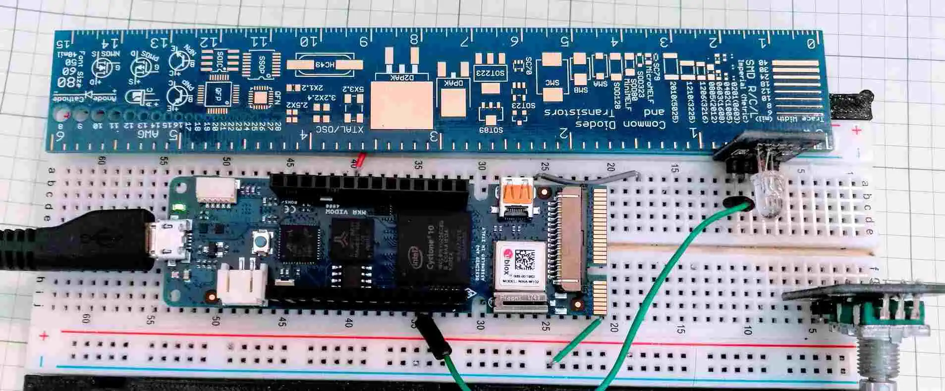
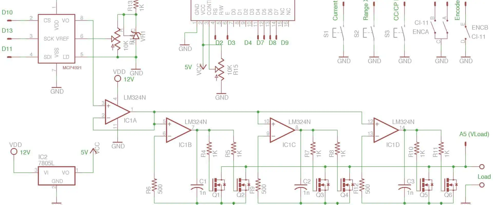
Designing an electronic load requires careful consideration of various factors, including operational amplifier selection, MOSFET selection, and board layout. Each of these factors plays a critical role in determining the overall performance of the electronic load. The following are the key considerations that designers must take into account when designing an optimal electronic load:

1. Operational Amplifier Selection

Op-amps, or operational amplifiers, are crucial parts of an electrical load. They amplify the voltage signal from the input and use it to operate the MOSFETs that supply the load to the test device. As a result, the selected op-amp can significantly impact the electronic load’s accuracy, stability, and noise qualities.

When choosing an op-amp for an electronic load

, designers must consider the required bandwidth, input voltage range, output voltage range, and noise characteristics. In addition, the gain bandwidth product, slew rate, and input offset voltage are additional factors to consider. Let’s examine each of these elements in more detail:

ร˜ Bandwidth:

The bandwidth refers to the range of frequencies the op-amp can work efficiently. For an electronic load, the op-amp must reliably amplify signals over a broad frequency range, from DC to several kHz. This requirement is crucial when checking power supplies or other gadgets that might contain a lot of ripple or noise.

ร˜ Input Voltage Range:

The input voltage range of an op-amp describes the highest and lowest voltages it can withstand without overheating or damaging. The input voltage range of an electronic load must be large enough to handle the range of anticipated input voltages from the test device.

ร˜ Output Voltage Range:

The output voltage range of an op-amp refers to the highest and lowest volts it can produce at the output. The output voltage range of an electronic load must be adequate to operate the MOSFETs and supply the required load to the test device.

ร˜ Noise Characteristics:

Noise characteristics refer to the quantity of unwanted electrical noise an op-amp introduces into a system. Low noise is necessary for an electronic load to operate steadily and with precise measurements.

ร˜ Gain Bandwidth Product:

Combining an op-amp’s gain and bandwidth forms its gain bandwidth product (GBP). Typically, a higher GBP indicates a better performance because the op-amp can sustain a high gain over a broader frequency range.

ร˜ Slew Rate:

An op-amp’s slew rate is the fastest rate at which its output can shift. Like GBP, a higher slew rate indicates a better performance since it means the op-amp can react to changes in the input signal more rapidly.

ร˜ Input Offset Voltage:

An op-amp’s input offset voltage is the voltage that you must apply at its inputs to cancel out the output voltage without an input signal. A lower input offset voltage typically suggests better performance because it allows the op-amp to produce more accurate output voltages.

2. MOSFET Choice:

MOSFET is the primary switching component in electrical loads. They must handle high currents and voltages while keeping low on-resistance and quick switching speeds because they act as the load for the tested device. When choosing MOSFETs for an electronic load, designers must consider several factors, including voltage rating, current rating, on-resistance, and switching speed.

  • Voltage Rating: The maximum voltage that a MOSFET can endure without malfunctioning is the MOSFET’s voltage rating.
  • Current Rating: The MOSFET’s current rating indicates the highest current that a MOSFET can manage without overheating or suffering damage. The MOSFETs in an electronic load should handle the maximum current the test device will likely draw.
  • On-Resistance: The channel’s resistance between the source and drain terminals when you switch the MOSFET on is its on-resistance. Better performance is typically possible with a reduced on-resistance because you can apply a more accurate load to the device you are testing with the MOSFET.
  • Switching Speed: The MOSFET’s switching speed describes how quickly it can flip on and off. Since the MOSFET can react rapidly to changes in the input signal, a faster switching speed typically suggests better performance.
  • Thermal considerations: To avoid overheating and harm, designers must ensure that MOSFETs undergo proper cooling while operating. It might be necessary to use heat traps or other cooling systems for this.
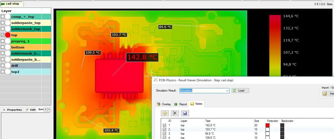
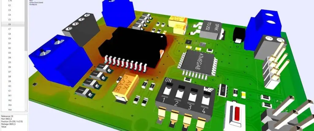
3. Board Design:

The board layout is crucial for an electronic load to work at its best. Unwanted noise, interference, parasitic capacitance, and inductance can all result from a poorly planned board layout, harming the load’s performance. Therefore, designers must consider several variables, such as component placement, ground layout, and thermal management, when creating the board plan for an electronic load.

  • Placement of Components: How you organize your components on a board can significantly affect how well a load works. To improve the precision and stability of the load, you should minimize the parasitic capacitance and inductance when placing components. Because the op-amp and MOSFETs are in charge of amplifying and controlling the load, their location is crucial.
  • Ground Layout: The board’s ground plan is essential for reducing interference and noise. A well-planned ground structure can lessen the effect of stray capacitance, inductance, and ground loops. To avoid ground loops and guarantee proper grounding, it’s crucial to ensure the ground plane has a secure attachment to the chassis or other ground points.
  • Thermal Management: Thermal management is essential because MOSFETs produce heat while operating, so designers must ensure they have a proper cooling system to avoid overheating and harm. It might be necessary to use heat traps or other cooling systems for this. In addition, the board architecture must efficiently transfer the MOSFETs and other heat-generating components away from the board.

Applications of Electronic Load Design

FULL PCB MANUFACTURING Quote

The following are the various applications of electronic load design in different industries:

1. Automotive:

Electronic loads in the car sector help test battery management systems, charging systems, and DC-DC converters. In addition, electronic loads help model the electrical loads of different vehicle components, such as lighting systems, power windows, and other electronic devices, in automotive applications. This capability aids in ensuring that the electrical system of the car is in good working order and can support the load demands put on it.

In addition, the testing of electric and hybrid cars also employs electronic loads. The battery management system (BMS) is essential to these vehicles. It controls the battery pack’s state of charge, monitors it, and ensures the battery is working within safe parameters. The BMS can precisely track the battery’s performance by simulating the weights on the battery pack using electronic loads.

2. Computing:

The computing industry also employs electronic load designs in testing power supply circuitry used in servers, workstations, laptops, and other electronic devices. Moreover, they also simulate the different loads that a computer system might encounter, such as the CPU, hard drive, and graphics cards. This step aids in ensuring that the power supply is safe to use and can support the demands put on it.

Electronic loads can also evaluate the thermal performance of computer systems in addition to power supply circuits. Electronic loads can assist in identifying parts of the system that may be prone to overheating by simulating the heat produced by different components.

3. Aerospace:

In aerospace, electronic load designs help test power supply circuits and electrical parts used in aircraft and spacecraft. In addition, these designs help simulate electrical loads of different components, including avionics, navigation, and communication systems. This action makes it easier to verify that the electrical system is reliable and capable of supporting the demands made on it.

Additionally, electronic loads are helpful when evaluating satellite power systems. Solar cells that turn sunlight into energy power satellites. To correctly model the performance of the electricity system, engineers simulate the loads on the solar panels using electronic loads.

4. Telecommunications:

Electronic loads are frequently applicable in the telecommunications sector for testing power supply lines and backup power systems used in cell towers, data centers, and other communication infrastructures. Additionally, they simulate electrical loads of different components, including routers, switches, and servers. This action aids in ensuring that the power supply is safe to use and can support the demands put on it.

Electronic loads can evaluate the thermal efficiency of communication infrastructure and test power supply circuits. In addition, electronic loads can aid in locating parts of the infrastructure that might be vulnerable to overheating by simulating the heat produced by different components.

5. Electronics

Testing power supplies, batteries, and renewable energy systems are just a few of the many electronic uses that employ electronic loads. In addition, electronic loads help model the various loads these systems might encounter, allowing engineers to precisely modify the system’s performance.

The testing of LED illumination systems also employs electronic loads. A steady current source is necessary for LED lighting devices to operate correctly. Engineers can precisely predict the system’s performance by simulating the loads on the LED illumination system with electronic loads.

Conclusion

The proper operation of different electrical components and circuits depends on electronic load design. Electronic load design can help you optimize the performance of your system and ensure that it can handle the required load, whether you’re looking at power sources, batteries, or LED illumination systems. From the automotive to the aerospace sectors, electronic load design is an essential tool for any engineer or technician looking to evaluate the performance of their electrical components. Therefore, remember to include an electronic load design in your toolkit when testing and characterizing an electronic circuit or component. You’ll be happy you did.

How to program Arduino FPGA

arduino FPGA

From the growing Internet of Things to the arrival of artificial intelligence, field-programmable gate arrays are steadily making their way into the future of electronics. Field-programmable gate array development is getting increasingly popular across various sectors and applications due to its versatility and constantly declining cost. However, as gadgets grow smaller and more linked, some may be difficult to use, making development impractical. On the other hand, field-programmable gate arrays are frequently helpful in developing devices, so using a link to control the device from a distance might be advantageous.

FPGAs are ICs programmed to carry out a predetermined set of tasks. Because they are programmable, we can modify FPGAs to suit the unique requirements of various applications. On the other hand, Arduino is a microcontroller board created for quick and interactive electronics prototyping. Its open-source infrastructure accommodates a variety of initiatives.

FPGAs

A digital circuit known as an FPGA can carry out any logical operation. PLBs, or programmable logic blocks, are the building blocks of FPGAs and we can combine them to form any digital circuit. The PLB can produce a variety of logical functions, including AND, OR, XOR, and NOT gates. Furthermore, the PLBs can be suitable for maths operations and other tasks like memory storage.

The advantages of FPGAs over conventional digital circuits are numerous. Secondly, FPGAs are flexible and adaptable to various applications because we can reprogram the. Second, because FPGAs can carry out many tasks, they can take the role of various digital circuits. Third, complicated digital circuits that are not feasible with conventional digital circuits can consist of FPGAs.

YouTube video

Arduino

A microcontroller board called Arduino is ideal for quick and interactive electronics prototyping. Arduino software programs the microprocessor at the heart of Arduino boards. The libraries and tools included with the Arduino software make it simple to write and upload code to the microcontroller. In addition, the input and output pins of Arduino boards can connect to sensors, actuators, and other electronic devices.

Anyone without an electronics background can easily develop their projects with Arduino hardware and software. Moreover, because of their low cost and simplicity of use, Arduino boards are also well-liked among students and hobbyists.

Connecting an FPGA to an Arduino Board

arduino FPGA PCBA
arduino FPGA PCBA

Connecting the two parts is the first step in using an FPGA with an Arduino. The connection technique will vary depending on the specific FPGA and Arduino boards utilized. There are typically two ways to link an FPGA to an Arduino:

GPIO Pins: Using the General Purpose Input/Output (GPIO) pins on the Arduino board is the simplest method for connecting an FPGA to an Arduino. Several GPIO pins on most Arduino boards can interface with external electronics. First, determine the precise pins on both the Arduino and the FPGA that will be helpful for communication if you want to link an FPGA to an Arduino utilizing GPIO pins. Once you’ve located these pins, you can link them with pins or a unique PCB.

Shields:ย Using a shield is another way to link an FPGA to an Arduino. The capability of the Arduino board can increase by attaching Arduino shields, which are pre-built modules. A variety of FPGA shields are available for use in securing an FPGA to an Arduino. The ports on these shields often enable direct connection of the FPGA to the Arduino board.

Steps of programming Arduino FPGA

The Arduino FPGA is a versatile platform for designing and programmatically manipulating unique hardware circuits. You may create intricate digital systems with an FPGA that carry out particular operations, such as data processing, signal filtering, and control logic.

By utilizing a hardware description language (HDL) to create a hardware design, synthesizing the design into a bitstream, and uploading the bitstream to the FPGA chip, you can program an Arduino FPGA. Below is a thorough breakdown of each action.

Step 1: Install the Necessary Software and Hardware

Setting up your development environment is necessary before you can begin writing code for an Arduino FPGA. This entails connecting the Arduino FPGA board to your computer and installing the required software programs, such as an HDL compiler, synthesis tool, and FPGA programmer.

The Xilinx Vivado development suite, used for FPGA design and synthesis, is included in the thorough instructions on setting up your environment and installing the software available on the Arduino website. The next step can be after you have connected your Arduino FPGA board and installed the software.

Install the Arduino IDE after downloading it: You will develop and upload your code to the FPGA board using the Arduino Integrated Development Environment. You can download the most recent version of the Arduino IDE at the official Arduino website.

After installing the Arduino IDE, you must install the FPGA board support package. This package contains the files and libraries required for programming the FPGA board. By selecting “Board” from the Arduino IDE’s “Tools” menu, followed by “Boards Manager,” you can install the board support package. Find the FPGA board you’re using in the Boards Manager, then select “Install.”

Connecting Your PC to the FPGA Board: Use a USB cord to link the FPGA board to your PC. Your computer ought to recognize the board right away.

Step 2: Create a Hardware Design

The following stage is to develop an FPGA hardware design using an HDL, such as Verilog or VHDL. To build and simulate complicated digital systems using software tools, HDL describes the behavior and topology of digital circuits textually.

A text editor or an integrated development environment (IDE) that supports HDLs, such as Xilinx Vivado or Quartus II, can generate a hardware design. The circuit’s inputs, outputs, and functionality, as well as the connections and logic gates that carry it out, are defined throughout the design process.

After creating your hardware design, save it as a Verilog or VHDL file for the next stage.

Step 3: Write and Compile the Code

You can begin writing the code after designing and simulating the circuit. To create your code in the C++ programming language, utilize the Arduino IDE. The code should contain all the essential commands to control the various elements in your circuit, such as turning on and off LEDs or adjusting a motor’s speed.

You must compile the code after writing it to ensure no problems. A built-in compiler in the Arduino IDE verifies the code for syntax errors and other problems. Before going on to the next step, you must correct any mistakes.

Step 4: Upload the Program to the FPGA

You can upload the program to the FPGA after compiling it. The steps listed below will assist you in uploading the program:

Join the FPGA board and the J-Link programmer.

Use a USB cable to link the FPGA board to your PC.

In the Arduino IDE, select Sketch > Upload Using Programmer.

Hold off till the upload procedure is complete.

Remove the USB cord and J-Link programmer from the FPGA board.

Step 5: Test the Program on the FPGA

Testing the software after uploading it to the FPGA is crucial to ensure everything is operating as it should. To test the program on the FPGA, perform these steps:

Attach the input and output devices to the FPGA board: Sensors, motors, LEDs, and any other components the program interacts with can serve as input and output devices. Attach these gadgets to the proper FPGA board pins.

The FPGA board is powered by: Use a USB cable or an external power supply to attach the FPGA board to a power source.

Check the output on the linked devices: After connecting the input devices and turning on the FPGA, check the output on the connected devices to ensure the program is operating as intended. Confirm if the motor is spinning in the right direction and speed, for instance, if the program is to control a motor. Ensure the accuracy of the readings if the program is to read data from a sensor.

Make any alterations required: Go over the code to find any problems if the program is not functioning as it should. You might need to make changes to the code to correct any errors or improve performance.

Test the program using numerous inputs and scenarios: To completely test the software, use various inputs and scenarios to ensure it functions appropriately in various situations. For instance, test the program with various temperatures to manage a temperature sensor to ensure data reads correctly.

Iterate and enhance: After testing the program, make any necessary adjustments to enhance its functionality or performance. Then, keep testing and iterating until the programme satisfies all requirements and functions as intended.

Programming language used

FULL PCB MANUFACTURING Quote

Arduino

The Arduino programming language, a simplified version of C++ designed for beginners, is commonly used to create applications for the Arduino platform. For example, writing code for microcontrollers like the ATmega328P found in the Arduino Uno board is made simple with this language.

As opposed to this, FPGAs (Field Programmable Gate Arrays) are often programmed using HDLs like VHDL or Verilog. With these languages, you can describe hardware circuit behavior in a manner akin to how you would describe a software algorithm.

Yet some FPGAs also support high-level programming in C or C++, which we subsequently convert by a compiler into the low-level hardware description language. For people who are more accustomed to software programming, this method, commonly called high-level synthesis (HLS), can make it simpler to design FPGA applications.

While Verilog and VHDL are used to describe the behavior of digital circuits, their syntax and semantics are dissimilar. A brief description of each language is below:

Verilog:

In the 1980s, Prabhu Goel and Phil Moorby created Verilog, a high-level HDL. It is frequently helpful for digital design and verification. It has a syntax comparable to C. Modules, which are similar to the components of digital circuits, and are the building blocks of Verilog code. Complex digital systems can be built by instantiating and connecting these modules: many FPGA vendors and the semiconductor industry support Verilog.

VHDL:

The US Department of Defense created VHDL, also known as VHSIC Hardware Description Language, in the 1980s. We describe digital circuits and systems using this high-level HDL. One can create and couple the modules of VHDL code together to form intricate digital systems. Although VHDL’s syntax is more complicated than Verilog’s, it is more capable and expressive. As a result, most FPGA vendors support it, which is frequently helpful in safety-critical applications.

Because they enable you to describe digital circuits and systems abstractly, Verilog and VHDL are both utilized for FPGA programming. This makes designing and debugging digital circuits simpler, especially for intricate systems. Moreover, most FPGA suppliers offer Verilog and VHDL, and both have sizable toolchains and libraries available.

Examples of projects that use an FPGA with an Arduino

Arduino IOT

While Arduinos are microcontrollers created to offer a simple platform for creating interactive projects, FPGAs are strong devices that may help to implement specialized digital logic circuits. A powerful system that combines the programmability and flexibility of an FPGA with the usability and accessibility of an Arduino can come about by combining an FPGA with an Arduino.

FPGA-based audio processing

Practicing FPGAs for real-time digital signal processing (DSP) algorithms to handle audio signals is common. This is known as FPGA-based audio processing. The FPGA can perform filtering, equalization, compression, and many more tasks. The fundamental actions involved in FPGA-based audio processing are listed below:

  • Audio signal input: The FPGA may receive the audio signal by utilizing an ADC to collect it. The ADC can connect to the FPGA via a serial interface like SPI or I2C.
  • Algorithms for processing: The FPGA can run different DSP algorithms on the audio signal input. Hardware description languages such as VHDL or Verilog can help implement these algorithms.
  • Memory: The FPGA can have internal or external memory to hold the edited audio samples.
  • Export audio signal: A digital-to-analog converter can output the processed audio signal (DAC). The DAC can link to the FPGA via a serial interface like SPI or I2C.
  • Control interface: A user interface for controlling the audio processing algorithms can use an Arduino or another microcontroller. Other devices like sensors, buttons, and displays can receive input and output from the Arduino.

FPGA-based video processing:

Although technically possible, FPGA-based video processing with Arduino is not simple. Field programmable gate arrays, sometimes FPGAs, are extremely flexible integrated circuits that may carry out particular tasks. Because of their quick processing times and low power requirements, they are frequently helpful in video processing applications.

A popular microcontroller platform for do-it-yourself electronics projects is Arduino. It can be helpful to manage an FPGA handling video processing even if it is unsuitable for high-speed video processing.

You would need to:

  • Choose an FPGA board compatible with the Arduino to implement FPGA-based video processing using an Arduino. Various FPGA boards, like the Papilio DUO and the Mojo V3, may be controlled by an Arduino.
  • Create code in Verilog or VHDL to instruct the FPGA to perform the appropriate video processing task. For example, this might involve video compression, color grading, or image scaling.
  • Employ a communication standard like SPI or I2C to communicate data and commands from the Arduino to the FPGA. The FPGA can receive inputs from the Arduino through visual data or control signals.
  • Attach the FPGA board to the video input source and output display. The video data will be real-time processed by the FPGA, and the output will go to the display device.

A complex project requiring a thorough knowledge of digital circuit design, programming, and video processing algorithms, it is essential to keep in mind that implementing FPGA-based video processing using an Arduino. Nonetheless, it can be a fruitful endeavour that yields a high-performance video processing system with the correct knowledge and tools.

FPGA-based data acquisition

A high-speed data acquisition system that can sample analog signals with high precision and store the data in memory can happen using an FPGA. The Arduino can link with sensors and other devices to control the data collecting process and send inputs to the FPGA. You can adhere to the general steps listed below:

  • Use a hardware description language (HDL), such as Verilog or VHDL, to design the FPGA-based data acquisition system. Creating the proper input/output ports and building the logic circuits that will interface with the sensors or other data sources you wish to collect is required.
  • Use an FPGA development board, such as a Digilent Nexys or Basys board, to implement the FPGA design. To compile and program the FPGA, you must use a software toolchain like Xilinx ISE or Vivado.
  • Connect the Arduino and FPGA using an I2C or SPI communication mechanism. By doing this, the Arduino can interface with the FPGA and access the data the FPGA is capturing.
  • Create an Arduino program to show or save the data the FPGA collects. The Arduino has built-in libraries and routines that can help to show data on an LCD screen, save it to an SD card, or send it wirelessly over Bluetooth or Wi-Fi.

Generally, FPGA-based data acquisition systems can be more flexible and performant than conventional microcontroller-based systems, but they also need more design and implementation resources and technical know-how. If you’ve never programmed an FPGA, you might wish to start with easier projects and gradually advance your abilities.

Implications of Arduino FPGA for future projects and research

Integrating Field-Programmable Gate Arrays (FPGAs) with Arduino microcontrollers has several consequences for upcoming projects and research. For example, digital circuits known as FPGAs may carry out particular jobs or operations. Furthermore, for creating projects using sensors, actuators, and other electrical components, Arduino is a popular open-source electronics platform.

Increased Processing Power

Increased processing power is one of Arduino FPGA’s most important effects. FPGAs can process data in parallel and execute complicated operations in real-time. When paired with Arduino microcontrollers, the resultant system can do more sophisticated tasks that would be challenging or impossible for a microcontroller alone. Application areas for FPGAs include machine learning, audio processing, and image processing. Developers may build systems capable of performing intricate computations and making real-time choices by integrating an FPGA with an Arduino board.

Customizability

The customizable nature of Arduino FPGA is another result. FPGAs offer incredible customizability and we may program it to carry out particular actions or operations. This implies that the final system may change to meet the unique requirements of the project or research. For instance, an FPGA might help to create a unique encryption technique or to carry out quick data compression. Developers may design systems optimized for their unique requirements by employing an FPGA.

Real-Time Processing

FPGAs’ real-time data processing capabilities make them particularly advantageous for applications like robotics, automation, and signal processing. For instance, a robot’s motors may use an FPGA, and sensor data could process in real time. In addition, developers may build systems that can react to information in real time and make decisions based on that input by attaching an FPGA to an Arduino board.

Low Latency

By combining Arduino with FPGA, low-latency systems that process data in real-time and react swiftly to input can be created. For instance, a developer may utilise an FPGA to construct a bespoke digital filter to reduce noise from a sensor signal. The system created by combining an FPGA with an Arduino board can react fast to changes in the sensor signal and deliver a low-latency output.

Education

There may be educational ramifications to the FPGA and Arduino connection. For example, students may get knowledge of digital logic and programming and hands-on experience with digital circuit applications by utilizing an FPGA. In addition, students may also access various instructional materials, like tutorials, sample projects, and reference designs, thanks to the open-source nature of both Arduino and FPGAs.

Limitations of using an FPGA with an Arduino

Powerful digital devices known as FPGAs (Field-Programmable Gate Arrays) may be helpful for various functions. Conversely, Arduino is a microcontroller board frequently essential for DIY projects and quick prototyping. However, there are several restrictions to take into account, even if utilizing an FPGA with an Arduino can be a wonderful method to combine the processing power of the FPGA with the adaptability and simplicity of the Arduino:

FPGAs are more complicated than microcontrollers like Arduino in terms of complexity. FPGAs need expertise in digital design, and specific hardware and software are necessary to program them. Due to its intricacy, it may be difficult for novices to utilize an FPGA with an Arduino.

Power: Compared to microcontrollers, FPGAs consume more power. This means a more complex power supply may be necessary for an FPGA with an Arduino than an Arduino acting alone.

FPGAs are larger than microcontrollers in terms of size. If space is a limitation, as it often is with tiny projects or wearables, this can be a problem.

Cost: Compared to microcontrollers, FPGAs are often more costly. This can be a problem if your budget is minimal.

Not all FPGAs are suitable for use with Arduino boards. Ensure the FPGA you select is compatible with the Arduino board you intend to use.

Learning curve: FPGA programming requires a distinct set of skills than microcontroller programming. Learning the skills necessary to program an FPGA can be time-consuming, and some people may have a high learning curve.

Combining an FPGA with an Arduino can be effective, but doing so requires more work and expertise than utilizing an Arduino alone. However, you can use an FPGA’s flexibility and power if you’re ready to invest the time and money needed to learn how to use it.

What is PCB Thermal Resistance?

PCB thermal resistance

Heat can be produced on a circuit board due to certain components as well as the resistance inside the lines. If somehow PCB thermal resistance becomes large, such high temperatures might harm the board. Heat sinks and fans are options, but they are insufficient. Fans raise power consumption, and they also add weight to the PCB.

The best course of action is to create a thermal management strategy that takes thermal resistance as well as conductivity into account. To ensure that components function properly, this method should maintain the circuit board’s peak temperature nearer to the surrounding air temperature. Here, we’ve discussed PCB thermal resistance as well as how to optimize your designs for maximum heat dissipation.

YouTube video

Why Is PCB Thermal Resistance Significant and What Does It Mean?

Circuit board thermal conductivity is inversely proportional to PCB thermal resistance. It specifies how quickly or slowly the Circuit board materials let heat to dissipate from the source. It displays the pace at which heat moves from hot to cool areas of the PCB.

Thermal pads and thermal vias are two connections towards the copper planes, affect thermal resistance.

What Affects Your PCB Substrate’s Thermal Resistance?

fr4 thermal conductivity

The PCB’s copper components and the material properties of the substrate together define the heat resistance. Those two ought to help when establishing the board design’s thermal management approach.

The plan should demonstrate the following and aim to lower heat resistance:

  • The ideal arrangement of electrical components
  • Which components require cooling sinks or fans
  • Position thermal vias optimally close to hot components

Techniques for Testing PCB Thermal Resistance

Thermal resistance may be determined in three different methods.

Thermal Conductivity Measurement

Utilizing thermal conductivity is the most common way to measure thermal resistance. Resistance would be the opposite of conductivity, making it simple to calculate heat conductivity.

Guarded Hot Plate Technique

It is quicker and simpler to test the heat resistance of a fully constructed yet unassembled board to use this approach since the circuit board substrates were two-dimensional.

When heat flows from the hot locations to cooler areas, the two Circuit board sides are measured to determine their respective temperatures. It is a straightforward method for determining thermal conductance, that can be utilized later to determine resistance and thermal conductivity.

Design to Reduce PCB Thermal Resistance

The three methods for reducing thermal resistance are as follows.

Employ High Thermal Conductivity Materials

Using materials that have high thermal conductivity is the most efficient technique to lower PCB thermal resistance. Hence, copper in the plane layers should be used on boards containing hot components to create quick-heat, low-resistance flow channels.

Instead, for high-speed or high-frequency boards, employ the internal power or ground plane layers. They will serve many functions as they additionally help with isolation and offer EMI shielding from the outside.

Place the copper pads beneath hot components

Copper pads placed beneath hot components help deflect heat out of the upper layer. Their internal ground planes, which is often linked to these pads by vias, protects the components.

For optimal heat transmission, solder the parts into the thermal pads if the component has a thermal paddle that is die-attached. It is important to remember, nevertheless, that too large or many vias might make it possible for the solder to flow through it during the board assembly.

Utilize Heavy Copper

Copper traces that are thicker or heavier may carry greater currents with little resistance. If the pcb must operate at high power, thicker copper would keep temperatures low since resistance raises temperature.

Alternate Substrate Materials to Boost Heat Dissipation

FULL PCB MANUFACTURING Quote

Using different substrate materials is another efficient method of lowering heat resistance. FR4 is a common type of substrate material. It has a conductivity of around 1.0 W/m-K, which is far lower than that of ceramic and metal.

This figure is comparable to the conductance of other laminates that are compatible with high frequencies, such as Rogers and Isola.

The increased thermal conductivity of ceramic and metal substrates, however, makes them more desirable for thermal control.

Ceramic

Ceramic materials have thermal conductivities ranging from 20 to 300 W/m (m-K). It is therefore perfect for positioning underneath or next to hot electronic systems. It may also do away with the requirement for large heat sinks or fans.

Ceramics also have the benefit of having a thermal expansion coefficient that is more similar to copper than the FR4. Consequently, it decreases stress on the thin copper vias and traces. Unfortunately, the substance is brittle and rapidly fractures.

Metal Cores

A typical aluminum metal substrate for metal-core PCBs has a thermal conductivity of 239 W/(m-K). You can attach this sheet to nearby ground planes to generate a second EFI shielding surface. This metal core offers greater mechanical durability and adaptability than ceramic, adding to superior conductivity. Metal-core PCBs are typically used in high-power LED systems since the diodes produce a lot of heat.

Suggestions for Managing PCB Thermal Resistance for Manufacturing

While choosing PCB substrates and components, take temperature coefficient into consideration

The trace and component thermal resistance is determined by the material characteristics and components of the board, as was previously mentioned. As a result, you should pick PCB substrates as well as components with good resistance and temperature specifications. For rapid heat transmission from LEDs, aluminum serves as a better material compared to FR4, for instance.

Provide High Power Component with Enough Room

Sparingly place the heat-generating parts on the circuit board. This allocation ought to reduce any hot spots that could lead to problems during the assembly reflow process.

Employ Thermal Vias to Improve Heat Dissipation

To dissipate heat from the components, most especially the high-power SMD components, use many vias. Since they transmit heat away from the board surface, heat source, as well as components more quickly than buried, blind, or micro vias, through-hole vias were preferable to those.

The Thermal Management Plan You Have

One crucial component of designing a board is to have improved efficient thermal conductivity is defining the stackup. The overall PCB thermal resistance as well as subsequent rate of heat transfer in the board will be influenced by the materials utilized in the stackup. Heat from the components which create a lot of heat can be transported using the placement of the copper conductors as well as the usage of heavier copper.

Several design decisions may need to be made according to the setting where the board would be deployed.

Ensure the necessary components don’t cause too much noise in surrounding circuits while using active cooling techniques.

Creating a Thermal Management Plan

Heat will be transported throughout the circuit board more efficiently with the careful placement of the via thermal resistance calculator, the use of active cooling mechanisms like fans, as well as the proper arrangement of the components. By positioning active components from the board’s edge and avoiding grouping them inside one area on the circuit board with a lot of them, you can assist avoid hot spots.

The temperature distribution ought to improve even while operating when employed with the via thermal resistance calculator as well as planes within internal layers.

The ideal thermal management plan for your Circuit board can be determined with the use of a thermal simulation program. Tracking power loss across your PCB might help you understand how the PDN behaves as heat source. You may get a picture as to how heat would move across your board as well as the ultimate temperature distribution by using this information combined with power ratings of each component values plus the measurements for the PCB thermal resistance.

Enhancing FR4 Thermal Resistance

The most popular PCB materials are called FR4 and are characterized by the epoxy laminate. This FR4 has a very poor thermal conductivity as a result of this fabrication approach.

Thermal vias are among the low-cost methods designers can increase FR4 thermal resistance. The two conducting layers are connected via plated through holes.

Designers are able to increase the FR4 thermal resistance by inserting PTH vias in the right places. When the source of heat is immediately normal to a thermal via and has a diameter of 0.6 mm, it has a PCB thermal resistance standing at 96.8 ยฐC/W. The FR4 thermal resistance is significantly improved when the amount of thermal via is increased. For instance, the initial 270-mm2 board will have its thermal resistance drop to 12 ยฐC/W, which is a significant improvement of approximately 60% from the initial value.

Since this area normal to a heat source shrinks for open vias, the thermal resistance produced by the former is higher than that from the filled vias.

Makers of metal-core PCBs produce their boards in various ways. Solder mask, copper circuit surface, thermally-conductive dielectric layer, as well as a metal core layerโ€”typically an aluminum substrateโ€”are all visible when a one-layer MCPCB is examined.

Conclusion

You can design the thermal management plan which can help in controlling heat transfer in the board by selecting the appropriate pcb substrate material as well as component options. The thermal management approach can shift heat away out of each source of heat and lower the temperature of the printed circuit board by strategically placing copper components, elements, as well as interior plane layers.

What are Voltage Regulator PCB Designs?

Voltage Regulator PCB Design

Voltage control is a crucial component of power engineering and electronics. For our gadgets to continue working as intended, it is imperative that such voltage magnitude in-between the transmitting and receiving ends of the component stay consistent. Voltage regulation involves the idea of delivering a nearly constant voltage under various load circumstances.

This can relate to active interventions made by the voltage regulating circuit or passive characteristics like the drop in voltage along a distribution and transmission line. We’ll examine voltage control across transmission lines in more detail and go through several active voltage control techniques.

YouTube video

What Does a Voltage Regulator Circuit Mean?

The voltage regulator PCB design work to keep the output voltage constant. This happens despite changes in the load conditions or input voltage. The voltage regulator is often attached to power supply with variable output voltage. Connected to a regulator’s output, more delicate components like digital components, microprocessors, as well as other loads can rely on it to deliver a set voltage.

Also, voltage regulators have been most frequently utilized for the DC to DC conversion. While some also include AC to AC and AC to DC conversion capabilities. Switching and linear voltage regulators are really the two most common types.

Voltage Regulator PCB Design Types

Voltage Regulator PCB

Linear Regulators

An amplifier is used to regulate linear regulators, which employ a FET or BJT to maintain their supply voltage. Also, the amplifier modifies the transistor so as to maintain its consistent output voltage. This is achieved by comparing the regulator’s output voltage to a precise reference.

Output voltage of linear regulators is always reduced. The low dropout regulator can be described as a linear regulator having low drop-out voltages.

Since there isn’t any switching involved, the regulators produce less noise and work best for powering delicate circuits. Switching regulators, on the other hand, are intrinsically noisy since they switch often to maintain their output voltage.

The linear regulators could function with relatively low quiescent currents whenever they are appropriately constructed. Switching regulators employ intricate feedback mechanisms and ultimately consume more quiescent power. Such regulators may exhibit exceptionally high efficiency (90%) when acting as LDOs. Linear regulators have become less expensive and simple to incorporate to any layout. They don’t need a lot of parts or filters.

To assist in controlling its output voltage, the capacitor is typically installed throughout the output volt.

Switching Regulators

Using the power BJT or MOSFET switch, the switching regulator transforms an input Voltage level to a very more steady Dc output. Throughout order to lower switching noise upon that output voltage, every output out of the switching regulator often is filtered. Switch regulators come in three different flavors: These include boost or step-up, buck or step-down, as well as buck-boost (could provide step-down or step-up.

These switching regulators are often more effective since they may operate in either an on or off mode. Also, they can offer 90% or more efficiency, that is very challenging for most linear regulator to achieve unless they have been specifically made to function as LDOs.

This is very helpful when a high voltage is needed for the short time frame (for example, a camera’s backlight).

Because linear regulators become less effective, they typically generate more heat and require a heat sink. Heat sinks are often not required for switching regulators.

How to Select Voltage Regulators for PCB Design

FULL PCB MANUFACTURING Quote

Your PCB would require constant DC voltage for functioning effectively unless you are dealing with an entirely AC system. Regardless of whether the input voltages (line) and output currents (load) fluctuates, the voltage regulator PCB design delivers the required DC voltage having a constant magnitude. Certain power lines were louder than others, and some circuits seem to be more susceptible to electrical changes than others.

Each designer need to be able to select the appropriate voltage regulator of their board. Let us just examine the various DC regulator types and discuss a few things to bear in mind while choosing a voltage regulator PCB Design.

Key Factors to Consider while Selecting Voltage Regulators

How to select the voltage regulators for various applications is a topic I frequently encounter on forums. There isn’t one answer to the query. While searching for the voltage regulator, users should think about the following qualities; be aware that both linear as well as switching regulators fall under these categories:

Output voltage

You must utilize the switching regulators in boost mode if you require a step-up regulator. One regulator is generally employed for every supply when utilizing systems with several suppliers.

Regulators typically provide a constant output voltage, yet there are certain regulators on the marketplace that you can are using some customizable parameters.

Noise versus efficiency

While switching regulators produce more noise compared to linear regulators, they are more efficient. Whenever the regulator delivers a large current, unnecessary electrical noise might disrupt other circuits. It might be more challenging to obtain EMC certification if you wish your products to go on sale. It is preferable to use a linear regulator if other printed circuits on the board require a lot of power, such as components that are solely analog.

Choosing a regulator having excessive power losses might make achieving efficiency targets nearly difficult. Linear regulators are much less loud, but they are highly inefficient (apart from LDO), which means some power gets converted into heat.

Install heat sinks mostly on board whenever your regulator would operate at high currents. The switching regulators could be a preferable choice if there isn’t space on the circuit board for the heat sinks or when power dissipation becomes an issue.

Transient Response

There is a brief spike inside the output whenever the output current fluctuates fast. Before returning to the same voltage, this voltage regulator requires a while. This is referred to as a transitory reaction. Typically, its output capacitance as well as loads current determines its transient response. Its quick transient reaction guarantees that a regulator can supply the necessary power. Search for the required bypass capacitor on the output of the regulator in the component data sheet.

Layout Out Every Circuit Block

Since we can view the complete system architecture, humans can better understand how to arrange every circuit block inside the switching supply of power coupled with the system generally to guarantee safety and low EMI. While designing a circuit board layout, keep in mind the whole block diagram:

Sectional organization: Try to set out the board’s power supply in portions, just like you would other boards having several functional blocks. This is acceptable to carry out this process linearly, moving from either the input into the output throughout their block diagram.

Layout considering feedback: There will occasionally be feedback across sections, like in a precise high current regulator. To fill this ground gap present between each component, use optocouplers.

Follow ground paths for return: “Follow the ground return paths” is arguably the only rule in Circuit board which applies to all designs. Regarding power supplies, it’s crucial for locating potential hot spots for common-mode currents and maintaining low-loop inductance for every supply segment.

Pay close attention to the high voltage and current rails: High voltage as well as high current design are sometimes combined. The minimum distance between both conductors is determined by the greatest potential difference in-between them (see IPC-2221), and the minimum width necessary to maintain low temperature is determined by the current that the conductor carries (check IPC-2152 for the external or internal layers).

What are the Limitations of the Voltage Regulator Circuits?

Voltage regulators have the following drawbacks. Among the primary drawbacks of a voltage regulator PCB design deals with the fact that it is inefficient in certain applications since it dissipates a significant amount of current.

This IC’s voltage drop resembles the voltage drop of resistors. That voltage drop between both terminals, for instance, is 2V whenever the input of the voltage regulator is 5V and its output is 3V. As the regulator’s efficiency may be limited to 3V as well as 5V, such regulators can be used with lesser Vin/Vout differentials.

The projected power dissipation meant for the regulator must be taken into account in every application since high input voltages may result in high power dissipation, which can cause harm to different components due to overheating.

Another drawback is that, in comparison to switching kinds, they can only do buck conversion since these regulators offer both conversion and buck.

Although switching type regulators are very efficient, they have certain disadvantages, including being less cost-effective than linear type regulators, being more complicated, being larger in size, and being more noisy if its outside components are not carefully chosen.

Parameters of Voltage regulator PCB

Output Voltage and Input Voltage

Preferably, you are aware of a range of input voltages as well as the necessary output voltage for the task at hand. Each chip in a voltage regulator is intended to be utilized with a certain output voltage

Dropout Voltage

A dropout can be described as the smallest buffer in-between the input and output voltages. The least 2V dropout would be required, for instance, if you’ve got a 7V input as well as need 5V output. You require a smaller dropout when you think your 7V input would go below 7V.

Every voltage regulator chip’s output voltage and dropout are given. For instance, a variety of dropouts are accessible in the 5V voltage regulator. The  low dropout voltage regulators and even the ultra low voltage regulators would be necessary for circuits having a slight difference in between input voltage and the output voltage.

Device Sensitivity

A particular regulator may be needed to limit noise in very sensitive electronics like cellphones, wireless gadgets, and medical equipment that are battery-powered.

Response Time

The specialty voltage regulator with quick reaction times are accessible for applications like graphics cards, TVs, computers, printers, as well as embedded devices.

Power Draw

By utilizing linear voltage regulators, the differences between the output and input voltages is wasted by being converted to heat. Heat generation is probably not a problem when power use is modest.

Related Questions

What functions do voltage regulators offer?

Any electronic or electrical device that keeps a power source’s voltage within reasonable bounds is known as a voltage regulator. This voltage regulator is required to maintain voltages inside the permitted range that electrical equipment employing that voltage can tolerate.

What signs might point to a malfunctioning voltage regulator?

Signs of a Malfunctioning or Defective Instrument Voltage Regulators include flickering or dim gauges. Flickering or dim gauges are among the initial signs of a voltage regulator problem. Another is irregular or inaccurate readings. Inaccurate or irregular voltage regulator readings and an inoperative instrument cluster are further signs of a voltage regulator problem.

What occurs if a voltage regulator malfunctions?

Even the engine of your automobile might be impacted by a poor voltage regulator. For instance, if this auto component stops functioning correctly, you could notice that the car’s engine occasionally stalls or sputters. While you drive, it can also have problems accelerating.

Do you require voltage regulator PCB designs?

Among the most widely used electrical components, the voltage regulators are probably required in over 90% of devices. The voltage regulator is necessary unless you can power everything directly from battery power or from an external DC/AC adaptor.

Conclusion

If voltage has to be adjusted, voltage regulator boards are often present. For instance, an AC converter in wireless phones might reduce 120 VAC power to 8 VAC. The voltage regulator is then located inside the phone’s base, supplying the necessary DC voltage into the base’s electronics. There may be a DC to DC adapter built inside the phone. This makes use of the voltage regulator in supplying the right voltage for electronics. In summary, we can say that voltage control is a crucial component of power engineering and electronics. For our gadgets to continue working as intended, it is imperative that such voltage magnitude in-between the transmitting and receiving ends of the component stay consistent

What Does Solder Mask Bridge Mean and How Can You Prevent It?

solder mask bridge

Component soldering becomes more and more complex as electronic gadgets get smaller. This also works with the circuit boards getting more compact. The built board has a number of difficulties and flaws as a result of this intricacy. This solder mask bridge is a frequent problem when assembling these components.

The phrase “bridge” typically refers to a passageway or connecting two previously inaccessible locations. In the context of wireless communications, the provision of internet connections in-between both wired networks via a Wi-Fi connection is referred to as “bridging”. In this scenario, the wireless bridge performs the role of a client. It achieves this by connecting to the router and sharing Internet connectivity with the connected devices.

Yet, the word “bridging” inside the PCBA field refers to a completely other process when used in tandem with soldering. One form of problem that might happen while soldering is called solder bridging. It is a problem that could have an effect on production, call for reworks. This could possibly lead to irregular functioning in this field. It is important to know how to avoid solder bridging for the best board fabrication and performance. Therefore let’s examine solder bridging’s root causes in further detail and suggest ways to prevent it.

Let’s examine a solder mask bridge in more detail, along with its causes, the prevention, as well as its remedies.

YouTube video

How your PCB is impacted by the solder masking process

bridge soldering

After delving into the process of solder mask, let’s look at how it impacts your PCB. This solder mask affects PCB assembly as well as board quality, as was previously mentioned. The most noteworthy effects of the solder mask are explained below, please let’s explain them below.

Prevents solder mask bridges: Creates the solder dam in-between the solder joints as well as other areas of your board that are conductive, which could cause board damage or short circuits.

Reduced solder paste consumption: Makes it possible to utilize fewer solder paste during the soldering operation. Serves like an insulator in-between the board components, providing additional isolation of the PCB’s components.

Safeguarding the PCB: This prevents the introduction of pollutants that could be caused by handling this board. Resists oxidation, which could reduce the device’s operational lifetime.

Raising its breakdown voltage: may improve the value of breakdown voltage that the dielectric material of the board holds and offer further protection against corona or arcs that are frequently found on high voltage (over 1 kV) boards.

Preventing the development of the metal whiskers: aid in avoiding the development of tin whiskers, which are typically linked to lead-free solder and tin plating for different electronic components.

It goes without saying that the procedure for the solder mask has a significant impact on how easily your board may be manufactured and how it will perform in use. However, there are some circumstances in which a solder mask might not be feasible or desirable, such as with small parts as well as fine pitches present on the BGAs (ball grid array). It is advisable to consult your CM in order to make sure there won’t be any negative consequences on the performance or dependability.

What does a PCB solder mask bridge represent?

Two points are joined by a bridge. The solder mask bridge forms on circuit boards whenever extra solder links at least two pads that ought to be separated above your solder mask.

Because of this problem, electrical shorts are created that, depending on how the bridging points are used, might result in various types of harm.

Causes of Solder Bridging

Solder bridging can occur under various circumstances. These can be defective machinery, subpar manufacturing techniques, or bad designs. The most common causes include:

  • Using too much solder on the SMT pads because the stencil specifications were wrong;
  • Defective seals in-between the stencil and bare board during printing;
  • Relatively large designs for solder pad compared to that gap present between the pads;
  • Incorrect component placement;
  • Relatively small component lead sizes in comparison to pad size; insufficient solder resistant layers found between the pads.

The fact that the liquid solder usually wicks toward heated metal or melted solder must be remembered (a large part of this PCB assembly procedure relies heavily on that factor).

This phenomena happens due to the fact that reflowing solder features strong surface tension, thus it remains balled up wherever it ought to be when holding items in it. Bridging can be brought on by anything that alters the system’s normal behavior.

Commonly Known Issues of Soldering Bridging

FULL PCB MANUFACTURING Quote

Solder bridging could cause these problems.

Dewetting and Non-Wetting

Molten solder deciding to leave exposed copper on its pad is referred to as non-wetting. This problem typically arises when brass components have not yet been adequately plated or when the flux needs to be changed. On the contrary, dewetting indicates that molten solder covers a pad, then retreats, leaving the solder mound.

Pin Holes and Blow Holes

Both of these holes arise when the board has either poor plating of copper or an excessive amount of moisture.

Lifted Pads

Whenever the soldered component is removed from the joints with a worn-out soldering surface or one having an uneven layer of copper plating, lifted pads may appear.

Tombstone

Whenever the component is lifted all through wave soldering, it creates the tombstone problem and looks like one. Component lifting can be caused by using parts having different measurements for solderability or using leads of the wrong length.

Excess Solder

High solder accumulation could arise due to the improper lead size compared to the pad ratio. Additionally, it might be because of the conveyor belt’s rapid movement.

What You Must Do To Avoid Solder Mask Bridges?

While it’s not possible to ensure that there won’t be any solder mask bridges, one can avoid the problem by taking these precautions.

Verify the design of the circuit board again

Make sure that the design of the boards meets the best levels of producibility for the surface mount and through hole components. Also, you may work with the standards for the IPC industry for both the design as well as assembly of the PCB, which defines the A level as the best level for general productivity. In general, the most effective practice involves avoiding the tiny spacings or parts.

Asides that, check the design rules of the mask relief for areas which do not require the applications of the solder mask. We advice setting the relief to between 0.003 to 0.008 inches in the SMT components. However, you may need to adjust the value when the pads get extremely close together. Also, the color of the solder mask affects the relief.

Alter its Reflow Profile

By lengthening the period just above your liquid solder, the pads as well as component leads will have enough time to reach that same temperature. The solder would wet both once it reaches the desired temperature and moves there.

Leave Solder Mask Dams Between Pads

The solder mask dams are needed between the SMT pads due to the fact that it serves as the isolation wall, which prevents spillovers.In general, the minimum size of the dam should be about 0.004 inches.

For through-hole components, use the appropriate lead lengths.

The board’s thickness and size, the mass and size of the components, and the soldering type all affects the proper lead length.

This PCB manufacturer must assist you in determining the exact length needed for that application because long leads could result in bridging.

Minimize the Volume of the Solder Paste

One reason for solder mask bridges is the overuse of solder paste. Therefore, significantly less bridging can be achieved by reducing the volume of the solder paste or altering the stencil in order to change the location of the application.

Employ Solder Mask Specified Pads for the Tight Regions

You can choose the solder-mask-defined pad for protecting the surface for soldering if there isn’t enough space available for barrier and mask relief and you do not require the solder mask dams.

Use the Proper Pad Diameter and Hole Size

A solder mask bridge is more likely to form when there are big copper pads or through holes between the adjacent surfaces for soldering.

Apply the Solder Masking Properly

Any areas of the PCB which do not require soldering have a solder mask placed as its top layer. Molten solder won’t stick to epoxy, which is a common type of mask material. Therefore, you have to apply that mask in-between the component pins so as to stop the solder from forming the solder mask bridge.

Utilize Fiducials on the PCB

The fiducials are the markets placed on the circuit board design, which allows the automated machine to locate your PCB, and then align it properly. It will also place these components perfectly. The misplaced parts would also increase the solder mask bridges chances and then the marks will aid in the elimination of the problem.

Team up with a well-known PCB Manufacturer

Once you are done sending the files for the design to your manufacturer, then you have no control over the processes of fabrication, as well as assembly.

How You can Fix the Solder mask bridges

Root cause of Solder Bridging

Before you can solve the solder mask bridge issue, you must have a solder flask, solder wick, as well as a soldering iron that is heat adjustable. Having all these, you can get rid of the problem using the steps below.

Monitor Its Temperature

The tip of the soldering iron must transfer the required heat for your solder wick to be able to melt as well as absorb that solder. Therefore, thereโ€™s a need to keep monitoring the temperature as well as ensure that it surpasses the temperature for soldering by some degrees. Take for instance, soldering at 250ยฐC, increase your temperature to about 270ยฐC. The higher temperature would cover for the heat absorption of the wick from its solder joint.

Make use of Surface Tension

The surface tension of molten solder can be used to detach the bridge with no need for a wick. Make use of a soldering iron having a clear top, but take care not to overheat the ICs or pads.

Make use of the Solder Wick

To absorb this melted bridge, we suggest utilizing solder wick. Add solder flux, position the wick well over bridge, and carefully heat with an iron. To transfer heat, lightly press your iron over that wick. Remember to replace the wick when it gets clogged.

It is essential to prevent overheating the PCB or the components. Additionally, removing this bridge may result in the removal of the solder joint; if this occurs, apply additional flux then solder that part neatly back to the board.

Frequently Asked Questions

What exactly are Solder mask bridge Jumpers?

Solder mask bridge jumpers are pairs of pads on the trace of a circuit board that can be bridged by a solder balls. To make the bridge, you may additionally utilize the 0-ohm resistor. Certain bridges, however, do not require soldering or joining and should stay open for various uses.

How Do You Solder Pads Together?

As previously indicated, you may bridge the solder pads with the solder ball or the 0-ohm resistor.

What does a faulty solder junction imply? 

A poor solder joint indicates one with insufficient solder. Inadequate solder makes that joint weak, increasing the likelihood of cracking and failure. This flaw can be corrected by warming the junction and applying extra solder. This strengthens the joint sufficiently.

What exactly are disturbed joints?

Disturbed joints are usually caused by movement even during the alloy solidification. The final joint appears frosted and has a ripple structure on its surface. The movement might be manual or automatic. You can fix this issue by reheating these joints and allowing them to cool properly.

Conclusion

In summary, solder mask bridges could be harmful to the circuit boards owing to shorting. Therefore, you ought to take the precautions outlined above to prevent them. Nonetheless, if they do develop, a quick solution is possible.

Why TQFP Package is an Ideal Package Option for Integrated Circuits

TQFP Package

Integrated circuits are usually packaged differently. IC packages encase and protect the circuit material from physical damage and corrosion. These packages are available in different types. Also, there are different ways to classify these packages.

The most common materials used in packaging integrated circuits are ceramics or plastics since they feature improved electrical conductivity. Our main topic focuses on the TQFP package, a type of IC package.

What is a TQFP Package?

A TQFP package is a type of IC package which refers to tin quad flat package. This IC Package has a smaller footprint. As the full name of TQFP suggests, this IC package is a thin variant of the quad flat package. TQFP package has gull wings which extend from all the sides of the package. This package is available in various body size ranging from 5m square to 20 mm square.

The TQFP package features the same footprint as the LQFP. This indicates that these two IC packages have the same size. Also, there are a variant of the quad flat packages. Despite their similarities, the leads of TQFP are shorter than that of LQFP. TQFP has proved to be very useful when reducing the overall PCB thickness.

YouTube video

It is a perfect option when you need to make a printed circuit board more compact. The gull wings present in TQFP package extends from all the four sides. This package is one of the thinnest IC package in the market. The pin counts of this IC package starts from 32 to about 256 pins. Its body sizes also ranges from 7 x 7, 14 x 14, and 10 x 10.

TQFP packaging process requires the use of a low loop wire bonding process and a good package control. The IC packaging process integrated in TQFP packaging is the flatpack package. When Quad Flat Package (QFP) gained popularity, this package was commonly used in Europe. However, the QFP became popular across other countries like the United States.

Presently, the USโ€™ military standard for surface mount components packaging in circuit boards is the flatpack package. The TQFP package is ideal for electronic projects that need cost-effective, reliable packages.

How TQFP Package Tackles Some Industry Problems

Spartan 6 TQFP Package

TQFP is a reliable IC package widely integrated in printed circuit boards. This type of IC package has helped to provide solutions to some common problems in the industry. TQFP package solves problems associated with PCB designs. Below are some of the problems solved by this package

Die shrinking

TQFP package provides a long lasting solution to die shrinking. Die shrinking occurs when the design chip contents i.e the geometries for he layout of the die shrinks down to a smaller node to help in minimizing the footprintโ€™s size in a package. TQFP package makes die shrinking less noticeable below where it is positioned.  

TQFP package prevents die shrinking through the enhanced thickness of the die wire.

IC package portability

Some IC packages are not portable. With TQFP packages, it is possible to get the portability needed. This is because of the thinness of its quad flat package.

Benefits of TQFP IC Package

There are several advantages of using the TQFP package in printed circuit boards. These advantages give them edge over other type of QFP packages.

Suitable for smaller electronic devices

Due to the thin profile of the TQFP, this package is ideal for use in smaller electronic devices. They help PCB manufacturers to fabricate smaller circuit boards which are used in smaller electronics.

Environmentally friendly

TQFP package comprises green materials. The materials used in the production of this IC package are lead-free and as such it is environmentally friendly. Also, this makes TQFP package RoHS compliant and as well standardized.

Smaller package form factor

This is another advantage of TQFP. The TQFP package has a smaller package which makes it ideal for high frequency applications. Also, its reduced parasitic parameter is a big advantage of this IC package.

Package reliability

An IC package should offer the necessary reliability needed for its utilization in certain applications. TQFP package has several pin counts which makes it a reliable option. The numerous pin counts help this IC package perform better in several applications.

TQFP keeps providing benefits for engineers and designers. This cost-effective package delivers mechanical and thermal stability.

Limitations of TQFP IC Package

FULL PCB MANUFACTURING Quote

Despite the benefits of this IC package, it has got its won limitations. Therefore, PCB manufacturers need to expect some design challenges when integrating this package on their PCB projects. Some of the limitations of TQFP package include:

Solder bridges problem

For a TQFP package, the spaces need to be decreased form more pins. In as much as this sounds as a good idea, there are some problems associated with this. Decreasing the spaces for more pins has placed more demands on soldering. Therefore, PCB manufacturers are more likely to experience solder bridges when using the TFQP package.

Minimized spacing

Another disadvantage of using the TFQP package is decrease spacing. Amongst the quad flat package types, TQFP has the smallest spacing. This is because of the reduction of spaces available. The available spaces have been reduced from 50 mil to 20 mil and 12 mil. The reduction in spacing helped to provide more spaces to add more pins. However, this has posed some problems.

Possible Challenges Associated with Working with TQFP

Designers and engineers can encounter some possible challenges when working with the TQFP package. Due to these challenges, TQFP isnโ€™t straightforward. Therefore, you will need to pay attention to some of these problems while working with this package.

Avoid mishandling the pins

The pins on TQFP are small and have little spacing. The little spacing and small pin size can cause damages, especially when the pins are mishandled in the packaging process. Therefore, it is crucial to keep the pins in a safe position. You can make use of the pick and place machines for the whole packaging process. These machines reduce errors by eliminating human inputs in most aspects of the design. Also, these machine perform their functions without damage.

Another way to avoid mishandling the pins is careful storage. It is advisable to store the pins in a safe place. You can request for proper storage as this keeps the pins protected from any form of damage.

Be careful with the TQFP pins

TQFP packages have more pins which helps in increasing the density of this package. However, it can result in some possible issues. For instance, you want to maintain proper spacing between one pin and the next pin. Doing this will help in preventing any overlap in the performance of the pin.

Benefits of SMT Integration in TQFP

Surface mount technology (SMT) is a packaging type for TQFP. The integration of SMT in TQFP offers these benefits:

Improved EMC performance

EMC also referred to as electromagnetic compatibility refers to the capability of electronic devices and components to perform well despite their proximity.

Automated methods

Surface mount technology integrates automation to place components on a PCB. This automation minimizes human inputs and as such, saves costs.

Applications of TQFP

TFQP is the thinnest quad flat package. It offers a wide range of benefits and as such, it is widely used in various applications like

  • Semiconductor applications like gate arrays and microcontrollers
  • Computing applications
  • Communications boards such as integrated service digital network and Ethernet
  • Telecommunications
  • Chipsets for Laptops and Tablets
  • Video/ audio applications
  • Data acquisition

Frequently Asked Questions

SMD IC

What is the Difference Between TQFP vs LQFP?

The TQFP package features the same footprint as the LQFP. This indicates that these two IC packages have the same size.. Despite their similarities, the leads of TQFP are shorter than that of LQFP. While TQFP stands for Thin Quad Flat Package, LQFP stands for low-profile flat package. Also, there are a variant of the quad flat packages. TQFP has proved to be very useful when reducing the overall PCB thickness.

LQFP is easier to mount due to its longer leads. The lead count range of TQFP is between 32 to 176 while that of LQFP is between 32 to 208. TQFP is usually compared to LQFP due to their similarities. However, the main difference between these two IC packages is in their height. LQFP has a height that is about 1.7mm while the height of TQFP is less than 1.2mm.

How does TFQP Integrate Limited Spacing With More Pin Counts?

The thin quad flat package features limited spacing, however, this package type makes up for this weakness by using more pins. TQFP can use certain gate arrays like the Pin Grid Array and Ball Grid Array packages. This integration helps in minimizing the challenges that comes with spacing the leads. Also, it enables smooth connections around the package and as well as improve the pin count of smaller IC packages.

Conclusion

TQFP is a good IC package option that has proved to be effective. As a variant of the quad flat package, it features a very small footprint. This IC package has its advantages and disadvantages. We have explained how TQFP works and its use cases in this article.

Tips and Tricks to Build Efficient 433mhz PCB Antenna Design

433mhz PCB Antenna Design

Antenna-printed circuit boards are generally gadgets that technicians utilize to transmit and receive signals. Hence, these gadgets are heavily used in the telecommunication industry. Moreover, with the emergence of the 5G network, more and more electrical and electronic devices will bear antenna-printed circuit boards to communicate effectively. Moreover, printed circuit board antennas will also help technicians achieve full integration of home gadgets via the Internet of Things (IoT), which connects communicating devices.

However, to achieve all these, technicians must first overcome the barrier of designing the printed circuit board antennas. And when it comes to designing printed circuit board antennas, the 433mhz tops the list in terms of the trickiest PCB antennas to design. That is because these antennas have multiple constraints, which make them challenging to design and get right in terms of high performance and reliability. So how can you design 433mhz PCB antennas that are not just functional but also reliable? And are there shortcomings that come with dealing with 433 PCB antennas?

YouTube video

Understanding Antennas Printed Circuit Boards

We are in an era that is slowly moving towards wireless tech. Currently, most, if not all, electronic gadgets are relying on wireless tech heavily. For instance, major electronic gadgets we utilize to achieve our daily tasks, such as pads, laptops, and smartphones, rely heavily on this technology. That is because antennas printed circuit boards are crucial elements that allow effective reception and transmission of EM (electromagnetic) radiation under unrestricted spaces.

Printed circuit board antennas are the most popular variation of antennas in printed circuit boards. Generally, these antennas are printed onto a bare board that bears copper ink. Moreover, the bare board that holds the antennas tends to have electrical connections to other electronic components, for example, resistors or connectors. It then utilizes these connections to receive or transmit EM waves.

Antenna-printed circuit boards are wireless gadgets that receive or transmit signals. These components have multiple applications in the communication (telecommunication) industry.

Basics of Antennas

mhz PCB Antenna Design

FPC antennas represent exposed conductors. And conductors transform into antennas when they gain a specific ratio. They also turn into antennas when they become an element of a wavelength signal. The conditions that turn conductors into antennas are known as resonance because the electrical energy that is fed by the antennas is generally released into the atmosphere.

The geometry of an antenna possesses two crucial aspects in the following areas:

  • The antenna feed
  • The antenna length

In printed circuit boards, antennas achieve similar levels of performance to dipole antennas. They operate by having the ground located slightly beneath the conductor. Placing the ground at this level generates a unique image of a pretty similar length. Generally, the legs operate as dipole antennas, which experts call wave monopoles.

Therefore, when generating a printed circuit board design, you should significantly consider the following factors:

  • The ground plane
  • The return pathโ€™s shape and size
  • Type of antenna
  • Antenna length

Categories of Antennas

There are there man antenna categories, and they are:

  • Chip Antenna
  • PCB Antennas
  • Wire Antennas

Wire Antennas

Generally, this category encompasses antennas that have wires extending from the PCB and into the environment. However, the length of this antenna matches around a quarter length over the G-plane designation. Moreover, this antenna feeds off a 50 ฮฉ four TL (transmission line).

These types of antennas offer the best performance and RF range due to their attributable dimensions and three-dimensional exposure. In addition, these wires can deliver a helix, a straight, or a loop.

Printed Circuit Board Antennas

PCB antennas also go by the name PCB Trace Antennas since they involve drawing a trace on a printed circuit board. Moreover, these antennas can come in varying traces shapes which might include:

  • Wiggly curve
  • Inverted F-type trace
  • Circular trace
  • Straight trace meandered trace

These shape variations come due to antenna and shape constraints. Moreover, PCBs become 2D structures which makes them similar to standard printed circuit boards in terms of appearance. However, you must follow specific guidelines when bringing three-dimensional antennas and transitioning them to two-dimensional printed circuit board traces.

Chip Antennas

Chips antennas come as small (minuscule) form-factor IC (integrated circuits) which possess an antenna. These antennae are pretty useful when gadgets don’t have sufficient space to hold printed circuit board antennas. Moreover, these gadgets also support three-dimensional wire antennas, which makes them pretty efficient.

Materials Used to Generate Printed Circuit Board Antennas

FULL PCB MANUFACTURING Quote

For a component to qualify as an antenna printed circuit board material, it has to bear a high frequency. That’s because normal components can’t perform well when used in antenna-printed circuit boards. Here is a list of common materials that you can utilize to generate your antenna printed circuit board:

These materials are available in the market, and you can access them easily using the internet. Moreover, you can also contact a PCB antenna manufacturing company to purchase these components from them.

Significant Antenna Types PCBs

The Antenna printed circuit board designing and fabrication process involves experts first understanding the many variations of antenna PCB that exist and their unique applications. Generally, you can’t produce or design something you know nothing about or its specific application. As seen earlier, there are three significant categories of antenna-printed circuit boards. However, you can transcend this classification to get multiple types of antenna printed circuit board variations.

The significant types of antenna PCBs include:

Printed Circuit Board Antennas

The printed circuit board wifi antennas offer customers reliable and easy-to-drop solutions for simple yet efficient wifi communication integration. Moreover, these antennas are customizable, which means you can manipulate them based on your cable length and connector type specifications.

The printed circuit board wifi antenna provides 4G and 5G ranges beside bearing an effective IPEX connector for impeccable connectivity.

Attributes of the Printed Circuit Board WiFi Antenna

The printed circuit board wifi antenna comes bearing the following attributes:

  • Adhesive backing
  • PCB or FPC
  • 10 N of pull force
  • 50ohm impedance

The PCB Bluetooth Antenna

The printed circuit board Bluetooth antenna is an efficient instrumental component that allows various functionalities, which include:

  • Bluetooth connection
  • Bluetooth pairing

Moreover, these antennas come connected to various gadgets, for example, laptops and smartphone, and it has proven to be flexible and robust. Furthermore, this antenna has over 70% efficiency across various bands, on-ground and off-ground.

Attributes of the PCB Bluetooth Antenna

The printed circuit board Bluetooth antenna comes bearing the following attributes:

  • A rugged, cost-effective design that allows for a reel, SMT, pick and place, and tape packaging
  • It is an off-the-shelf electronic product
  • Extensive application support
  • Design collateral
  • The off-ground and on-ground solutions
  • High performance even though it is an embedded solution
  • It is a printed circuit board embedded structure that comes with complete ground clearance. Moreover, it also has small form factor needs.

The 433 MHz Printed Circuit Board Antenna

The 433 MHz printed circuit board antenna, which is the main focus of this article, is among the major types of printed circuit board antennas. These antennas come with single-chip radio frequency transceivers that feature FSK modulation and demodulation capabilities.

These 433 MHz printed circuit board mostly find their primary application in various UHF radio gadgets as compliance requirements, especially by the ETSI specifications. Moreover, these antennas also apply in the following:

  • Wireless communication
  • Telemetry
  • Alarm and security systems
  • Toys
  • Automotive
  • Remote controls

Attributes of the 433 MHz Printed Circuit Board Antenna

The 433 MHz printed circuit board antenna bears the following unique attributes:

  • Standby mode
  • Wide range supply
  • Power intake is relatively low
  • They do not utilize many external components
  • Data coding isnโ€™t necessary
  • No setup or configuration
  • FSK and TRU single-chip transceivers
  • Two FBs (frequency bands)

Generating a 433MHz PCB Antenna Design

gsm pcb antenna
gsm pcb antenna

Generally, antenna designs tend to play a vital role when it comes to achieving successful short-range and low-power transceiver communication between various systems. Experts use the target operating frequency’s wavelength to effectively determine the size of the patch during the PCB antenna design process.

Moreover, when it comes to generating a 433 PCB antenna design, you should be ready to do some calculations since you will deal with multiple variables.

Calculating 433 MHz PCB Antenna Parameters

Before calculating the antenna parameters, you must choose the perfect substrate materials to use on the PCB. Moreover, you also have to select the ideal width and length of the materials needed along the antenna’s operating frequency. Note that when you are dealing with the 433 MHz printed circuit board antenna, you should utilize FR4 material since it has a permeability of 4.4 and a relatively high dielectric strength.

When it comes to broadening the antenna, you should highly consider the substrates height. Actually, it would help if you kept the substrate’s height constant throughout your design process.

If you go with materials such as Bakelite and Glass epoxy, you should maintain the substrate’s height at around 1.5 mm.

As per traces, you should design and calculate the impedance traces, power traces, and signal traces carefully and with much precision because an improper trace width can generate an excellent signal reflection. Moreover, you should note that the minimum TW (trace width) should be 0.625mm or six mils. But if you are aiming for high tolerance, then you should keep the trace width at the following ranges:

  • 0.254 โ€“ 0.3 mm
  • 10 โ€“ 12 mil

Moreover, when carrying out trace calculations, you should remember that trace resistance tends to go higher as the board’s trace gets narrower or longer. Therefore, you should keep traces carrying relatively higher current short to maintain high performance.

Designing the actual Antenna

Antennas are pretty sensitive to the environment. Therefore, when you embed them on a printed circuit board, you have to consider various constraints and requirements highly. That is because these requirements significantly impact the reliability and performance of your 433 MHz printed circuit board antenna.

Therefore, when generating a design for a 433 MHz PCB antenna, you have to keep the following in mind:

Positions the Antenna

Different antennas have varying modes of operation. Moreover, depending on the radiation levels of an antenna, you might have to position it in a specific area on the printed circuit board. In our case, you can place the antennas in the following positions:

  • The long side of your printed circuit board
  • The corner of the printed circuit board
  • Or lastly, the short side of the printed circuit board

Keep Out Areas

When designing the areas to hold the components, ensure you place them away from the antenna area. That is because positioning components near the antenna might lead to signal interference, ultimately leading to your gadget performing poorly.

Moreover, note that the section around the board’s antenna should be away from any metallic object, including mounting screws.

Ground Planes

Regarding the ground plane, you should significantly consider various factors, including the size of the GP (ground plane). That is because any cables you use for communication between multiple batteries and devices might alter the normal functioning of the device if you don’t design them correctly. Therefore, you must ensure you pick the perfect size for the GP.

Proximity

When designing the 433 MHz PCB antenna, you should ensure you keep the antenna away from electronic components in the circuit board. That is because the electronic components can potentially interfere with the antenna’s radiation. Moreover, you should keep in mind that the gap between various components and antennas varies according to the width and height of the component.

Conclusion

We are living in an era that is full of wirelessly communicating devices, and part of the reason why this is made possible is due to printed circuit board antennas. However, printed circuit board antennas come in many different variations, and each variation requires unique design guidelines. The 433MHz PCB antenna is part of the major types of printed circuit board antennas, and it requires great attention to get right in terms of design. Therefore we hope this article will help you generate an efficient and high-performance 433MHz printed circuit board design.

Unlocking the Power of Fr4 Density: A Comprehensive Guide

fr4 pcb

It is a widely used substrate substance in the production of PCBs and can be coated or uncoated. It is popular in the industry due to its cost-effectiveness and reliability.

FR-4 comprises a mineral filler, glass cloth & epoxy resin that laminates together. A Glass cloth gives mechanical strength and electrical insulation, while an epoxy resin offers chemical resistance & excellent thermal properties.

Due to its mechanical properties and cost-effectiveness, the fiberglass-reinforced epoxy composite is widely used as a substrate substance for printed boards. Furthermore, its good dielectric properties make it a suitable coating for PCBs.

Understand the Fr4 density PCB Industry.

Compared to epoxy glass/polyimide, which has a resin of thirty percent, FR-4 has a lower polish of twenty percent. These results in a lower dielectric constant, giving FR-4 superior signal transmission qualities compared to others.

FR4 is the popular choice among engineers due to its superior signal transmission qualities. This makes a sheet of FR-4 material. A widely used, cost-effective material for constructing electronic device cabinets such as computer racks. Additionally, it is commonly employed in building metal cases for electric equipment like power supplies & motor controllers for industrial actuators or motors.

Is Fr4 density the way to go?

fr4-3mm-PCB

FR4 has several advantages, such as its affordability, lightweight nature, and ability to provide electrical & mechanical stability. Additionally, FR4 is available in a variety of thicknesses. However, it may not be the optimal board substance for all appliances. For instance, when constructing a radio, it may be more appropriate to use high-frequency laminates. It is recommended that you compare the dissipation factor figures of various laminates to determine which one is most suitable for your design.

Why Is the use of Fr4 density in electronics? 

FR4 boards possess excellent thermal properties & remain stable and durable even when subjected to heat, without any warping or cracking.

Besides, Fr4 fiberglass and Epoxy Resin. FR4 fiberglass contains a sheet of fiberglass that provides its structure, while the epoxy resin substrate is responsible for delivering rigidity & other attributes.

The amalgamation of these two substances produces a high-density circuit board possessing excellent electrical properties, rendering FR-4 a suitable choice for insulation on PCBs.

Major Material Types of Fr4 Density

There are various variations of FR-4 based on the material thickness and chemical properties, including the FR-4 & G10. Here are some standard designations for an FR4 printed circuit board substance:

  • Standard FR4:  It is the prevalent form of FR4, offering excellent mechanical & moisture resistance, withstanding temperatures of around 140โ„ƒ-150โ„ƒ.
  • FR4 With High Tg: FR4 with a high glass transition temperature is well-suited for applications that necessitate more thermal cycling & temperatures exceeding 150 degrees Celsius. Standard FR4 can only endure temperatures up to around 150โ„ƒ, but FR4 having high glass transition temperature can bear more elevated temperatures.
  • High CTI: FR4 having high CTI exhibits superior thermal conductivity compared to regular FR4 substances, with a tracking index greater than six hundred Volts.
  • FR4 without copper laminate: A material that lacks copper in its FR4 laminate is non-conductive with remarkable mechanical strength, primarily appropriate for board supports and insulating boards.
  • G10: It is a robust core material with exceptional mechanical qualities, high resistance to thermal shock, excellent dielectric rates, and effective electrical insulation.
  • Fr4 circuit has two layers: The FR4 material comprises an interior fiberglass layer and an exterior epoxy resin layer possessing several properties such as:

Flame Retardant

To enhance their fire-resistant qualities, FR4 materials are blended with flame retardants. Both organic & inorganic treatments can be used for flame retardancy. Organic treatments comprise halogen compounds like bromine, fluorine, chlorine, & iodine, but inorganic treatments contain aluminum trihydrate (ATH). These compounds are useful for treating FR4 materials, rendering them fire-resistant.

Good Electrical Properties

FR-4 is a fiberglass-reinforced epoxy composite possessing commendable electrical properties, stiffness, strength & thermal resistance.

Low Moisture Absorption

FR4 material exhibits a low rate of moisture absorption, which implies that it does not alter its shape when exposed to high levels of humidity. This attribute renders it well-suited for applications in which exposure to moisture is expectable, like electronic devices & electrical components.

FR4 Material Thickness

When selecting a circuit board fabricator, the thickness(width) of the FR4 substance plays a critical role. Nonetheless, there are restrictions on how thick or thin the design can be. The typical thickness range for FR4 PCBs is between 0.2-3.2mm and changes depending on the product.

Application of Fr4 PCB Density 

FULL PCB MANUFACTURING Quote

Common applications for FR4 are:

  • Industrial Wear Uses
  • Arc Shields
  • Electrical Insulation
  • Transformers
  • Washers
  • Busbars  
  • Switches
  • Relays
  • Standoffs
  • Terminal Strips

Fr4 density Materials – IPC-A-600 Standards

IPC-A-600 is the guidelines that outline the specifications for producing rigid & flexible PCBs using FR4 materials. The policies cover the surface and subsurface of the base material and apply to all stages of the manufacturing process, including testing and inspection.

Benefits of Fr4 density Materials 

FR4 is a versatile laminate material that boasts impressive mechanical & electrical properties. With more mechanical strength, superior dielectric properties & excellent thermal stability, FR4 is well-suited for a wide range of applications. It is also resistant to chemicals, heat, moisture & most solvents, making it a reliable choice for many industries.

Other benefits of FR4 materials include:

  • FR4 is the cost-effective option over other same substances.
  • It has excellent electrical insulation features due to its greater dielectric strength.
  • FR4 is lightweight with a high specific strength.
  • It is resistant to moisture and has good temperature resistance.
  • FR4 is resistant to water, making it suitable for different PCB applications.
  • The standard thickness for FR4 PCBs is typically between 0.2-3.2mm.

So these properties can make FR4 suitable for use in diverse environments.

Limitations of Fr4 density Materials 

When incorporating FR4 boards into your projects, it’s important to note some of their limitations.

ยท Insulating Stability

FR-4 circuit boards have excellent insulating properties, but they are susceptible to damage from overloading high temperatures and extra electrical currents going through the circuit board. This can fail the board and cause a loss of proper functioning.

ยท Controlled Impedance

FR4 has a non-uniform dielectric constant that varies as frequency increases, unlike high-speed circuit board substances. High-speed substances have dk tolerances of less than two percent, while FR4 has more than 10% tolerances. Therefore, this poses a challenge in maintaining the impedance (capacitance) values for impedance circuit boards.

ยท Signal Losses

PCB design needs to consider signal loss, particularly in high-speed applications. However, FR4 material is not the optimal choice for these appliances due to its higher Df than high-frequency substances.

ยท Temperature Stability

FR4 boards have a limitation in their ability to withstand high temperatures. While they can handle temperatures up to a certain limit, exceeding this limit can harm the material.

General Properties of Fr4 Density  

FR4-PCB-Material

FR4 substrate has a wide range of features that make it a versatile material for PCBs in various environments. These properties include thermal conductivity, impedance matching, and low heat capacity. As a result, FR4 is commonly useful for most PCBs.

ยท Board Thickness

The PCB thickness is a crucial design consideration, influenced by the board’s size and functionality. Thinner panels are suitable for compact equipment, USB connectors & Bluetooth accessories. However, for larger projects, we recommend thicker boards due to narrow FR4 circuit board limitations. 

ยท Moisture Absorption

Moisture absorption is a crucial property to consider while designing a circuit board. It refers to a material’s ability to resist moisture and determines how much humidity it can bear without degrading. Moisture absorption is measurable as the percentage of PCB material. FR4 has very low moisture absorption, only 0.10 percent when submerged in humidity for twenty-four hours. Hence, it is a perfect option for utilization in electronics fabrication.

ยท Glass Transition Temperature

The Tg of FR-4 falls within the range of 115-200ยฐC, depending on the production process & resins used. Standard FR-4 PCBs consist of an FR-4 layer sandwiched between two laminated copper coatings. One of the advantages of FR-4 is its fire resistance due to the presence of bromine. FR-4 has largely swapped G-10 compounds in an electronic circuit because of its lower price, superior mechanical strength & excellent insulating properties in dry and humid environments.

FR-4 classification and its electrical & physical properties are defined by the National Electrical Manufacturers Association LI 1-1998 standard. Each FR-4 substance has a composition and structure. The primary fiberglass layer provides FR4 with its stability, while the fire-resistant epoxy resin provides its rigidity. Additionally, FR4 exhibits excellent mechanical & insulating properties in both dry & humid environments.

You can use FR4 as a basic insulating material for PCBs. A production company will construct the board on an FR4 circuit board and composite it with a copper sheet to create the final product. PCBs frequently have multiple sides and multi-layer solder resist. These solders resist layers make the circuit for an absolute top overlay layer and allow for V-grooves.


Factors to Consider While Choosing Fr4 density PCB

When selecting an FR4 printed circuit board, various factors should be considered. The most important factor is the durability and quality of a product. While some producers sell the products at a very affordable price, they may not guarantee product quality. To ensure you purchase a high-quality FR4 printed circuit board, it’s essential to read as many reviews as possible before making a purchase. Other factors include:

ยท Sheet Thickens

The sheet thickness is a crucial factor in determining the number of layers that your board can have. Thicker sheets are more durable and ideal for high-density interconnect boards.

ยท Impedance Matching

It is a critical aspect of any electrical board, as it ensures that all components of your circuit function together seamlessly without any interference.

ยท Spacing

The current carrying capacity of a circuit board is affectable by the spacing between the copper traces. When the trails are too close, the board’s ability to carry current decreases

FR-4 Material vs. Rogers Material 

fr4-tg150
  • The cost of Rogersโ€™s material is significantly higher than that of FR-4 substance.
  • Rogersโ€™s material has superior high-frequency handling capabilities compared to FR-4 material.
  • FR-4 material has a higher dissipation factor, leading to higher signal loss compared to Rogers material.
  • Rogers material offers broader Dk values, making it more impedance-stable than FR-4 material.
  • The dielectric constant of Rogers material ranges from 6.15-11, while that of FR-4 material is approximately 4.5.
  • Rogers substance has a low-temperature variation than FR-4 material.

Wrap Up!

In conclusion, FR4 is a highly advantageous material due to its high strength, low weight & resistance to chemicals and fire. As a result, it has become a popular choice in the production industry.

If you require an FR4 producer for PCBs or boards manufactured by other substances, RayPCB can assist you. We offer quality boards & circuits in all quantities, prioritizing quality and timely delivery.

What is a PCB Dipole Antenna?

PCB Dipole Antenna

In the world of wireless communication, antennas play a crucial role in transmitting and receiving electromagnetic signals. Among the various types of antennas, the dipole antenna stands out as one of the most fundamental and widely used designs. When integrated into a Printed Circuit Board (PCB), it becomes a PCB dipole antenna, combining the simplicity of the dipole design with the convenience and cost-effectiveness of PCB manufacturing. This article delves into the world of PCB dipole antennas, exploring their characteristics, applications, and design considerations.

What is a Dipole Antenna?

A dipole antenna, in its simplest form, consists of two identical conductive elements, usually metal rods or wires, oriented end-to-end with a small gap between them. This gap is where the antenna is fed with the signal to be transmitted or where the received signal is extracted.

Basic Principles

The term “dipole” literally means “two poles,” which accurately describes the antenna’s structure. When an alternating current is applied to the feed point, it causes electrons to oscillate back and forth between the two elements. This oscillation creates an electromagnetic field that radiates outward from the antenna, forming the transmitted signal.

Resonance and Wavelength

A key characteristic of dipole antennas is their relationship with the wavelength of the signal they’re designed to transmit or receive. The most common dipole antenna is the half-wave dipole, where the total length of the two elements is approximately half the wavelength of the operating frequency.

Radiation Pattern

The radiation pattern of a dipole antenna is typically omnidirectional in the plane perpendicular to the antenna axis. This means it radiates equally in all directions in this plane, making it ideal for applications where the direction of the receiving antenna is unknown or variable.

Learn More about:

Typical Dipole Antenna

430-440MHz PCB Dipole Antenna

While the basic concept of a dipole antenna is simple, there are several variations and implementations, each with its own characteristics and use cases.

Half-Wave Dipole

As mentioned earlier, the half-wave dipole is the most common type. Its length is approximately half the wavelength of the operating frequency. This design offers a good balance of size and performance for many applications.

Folded Dipole

A folded dipole consists of a half-wave dipole with an additional wire connecting its ends, forming a narrow loop. This design offers higher impedance, which can be advantageous in certain matching scenarios.

Short Dipole

A short dipole is less than a half-wavelength long. While it’s more compact, it typically has lower efficiency and a different radiation pattern compared to a half-wave dipole.

PCB Dipole

This brings us to the focus of our article – the PCB dipole antenna. In this implementation, the conductive elements of the dipole are etched directly onto the PCB, offering a compact and cost-effective solution for many wireless devices.

Materials of PCB Dipole Antenna

The performance and characteristics of a PCB dipole antenna are heavily influenced by the materials used in its construction. Let’s explore the key components:

Substrate Material

The substrate is the base material of the PCB onto which the antenna is etched. Common substrate materials include:

  1. FR-4: A composite material composed of woven fiberglass cloth with an epoxy resin binder. It’s widely used due to its low cost and adequate performance for many applications.
  2. Rogers RO4350B: A high-frequency laminate that offers better electrical performance than FR-4, particularly at higher frequencies.
  3. Teflon (PTFE): Used in high-performance applications due to its excellent electrical properties, but it’s more expensive than FR-4.

The choice of substrate affects the antenna’s performance, particularly its efficiency and bandwidth. Materials with lower dielectric loss are generally preferred for better performance.

Copper Layer

The antenna elements themselves are typically made of copper, etched onto the PCB substrate. The thickness of this copper layer (often referred to as the “weight” of the copper) can affect the antenna’s performance and durability.

Solder Mask

While not directly part of the antenna, the solder mask layer can influence the antenna’s performance if it covers parts of the antenna elements. In many designs, the solder mask is removed from the antenna area to minimize its impact.

Surface Finish

The surface finish applied to the copper can affect the antenna’s performance over time. Common finishes include:

  1. ENIG (Electroless Nickel Immersion Gold)
  2. Immersion Tin
  3. Immersion Silver
  4. HASL (Hot Air Solder Leveling)

Each finish has its pros and cons in terms of cost, durability, and impact on RF performance.

What is the Range of a Dipole Antenna?

915mhz Dipole Antenna

The range of a dipole antenna depends on various factors, making it difficult to provide a single, definitive answer. However, we can explore the key factors that influence the range and provide some general guidelines.

Factors Affecting Range

  1. Transmit Power: The higher the transmit power, the greater the potential range.
  2. Receiver Sensitivity: A more sensitive receiver can detect weaker signals, effectively increasing the range.
  3. Frequency: Lower frequencies generally travel farther than higher frequencies in free space.
  4. Antenna Gain: Higher gain antennas can achieve longer ranges, but often at the expense of a narrower beam width.
  5. Environmental Factors: Obstacles, interference, and atmospheric conditions can significantly impact range.
  6. Height Above Ground: Generally, higher antenna placement results in better range.

Typical Ranges

For a PCB dipole antenna, typical ranges can vary widely based on the application:

  1. Bluetooth and Wi-Fi: In consumer devices, ranges are typically 10-100 meters, depending on the specific standard and environment.
  2. IoT Applications: Low-power IoT devices might have ranges from a few meters to several hundred meters.
  3. Amateur Radio: Half-wave dipoles used in amateur radio can achieve ranges of several kilometers to intercontinental distances, depending on frequency and conditions.
  4. RFID: PCB dipole antennas used in RFID applications typically have ranges from a few centimeters to several meters.

It’s important to note that these are general ranges, and actual performance can vary significantly based on the specific implementation and conditions.

How to Design a Dipole Antenna

Designing a PCB dipole antenna involves several steps and considerations. Here’s a general guide to the process:

1. Determine Requirements

  • Operating frequency
  • Bandwidth needs
  • Size constraints
  • Performance requirements (gain, efficiency, etc.)

2. Calculate Initial Dimensions

For a half-wave dipole, the total length (L) is approximately:

L = 0.5 * c / f

Where:

  • c is the speed of light (approximately 3×10^8 m/s)
  • f is the frequency in Hz

This gives the length in free space. For a PCB dipole, you’ll need to account for the effect of the substrate, which typically shortens the required length.

3. Choose PCB Material

Select an appropriate substrate material based on your performance requirements and budget constraints.

4. Simulate the Design

Use electromagnetic simulation software (like HFSS, CST, or ADS) to model the antenna and optimize its performance. This step is crucial for fine-tuning the design.

5. Impedance Matching

Design an appropriate feed and matching network to ensure efficient power transfer between the antenna and the radio circuitry.

6. Prototyping and Testing

Fabricate a prototype and test its performance using a vector network analyzer (VNA) and other RF test equipment.

7. Iterate and Optimize

Based on test results, refine the design and repeat the simulation and testing process until the desired performance is achieved.

Key Design Considerations

  • Ground Plane: The size and shape of the ground plane can significantly affect the antenna’s performance.
  • Nearby Components: Consider the impact of other PCB components on the antenna’s performance.
  • Manufacturability: Ensure your design can be reliably produced with standard PCB manufacturing processes.

DIY Dipole Antenna PCB

Dipole Antenna PCB

For hobbyists and enthusiasts, creating a DIY PCB dipole antenna can be an exciting and educational project. Here’s a simplified guide to get you started:

Materials Needed

  • PCB substrate (FR-4 is a good starting point)
  • Copper foil tape (if not using pre-clad PCB)
  • Etching solution (if creating your own PCB)
  • Soldering iron and solder
  • SMA connector (or appropriate connector for your application)

Steps

  1. Design: Create your antenna design using PCB design software. For a simple half-wave dipole, you’ll need two rectangular copper traces of appropriate length with a small gap between them for feeding.
  2. PCB Creation:
    • If using pre-clad PCB, etch your design using standard PCB etching techniques.
    • Alternatively, cut copper foil tape to shape and adhere it to a non-conductive substrate.
  3. Connector Attachment: Solder an SMA connector (or appropriate connector) to the feed point of your antenna.
  4. Testing: Use a VNA or SWR meter to test the antenna’s performance. Adjust the length if necessary to fine-tune the resonant frequency.

Tips for DIY PCB Dipole Antennas

  • Start with a slightly longer antenna than calculated and trim it to tune to the desired frequency.
  • Keep the feed point connection as short and direct as possible to minimize losses.
  • Experiment with different shapes, such as meandered lines, to reduce the overall size of the antenna.
  • Consider adding a simple matching network (like a series capacitor or shunt inductor) to improve the match if needed.

Remember, while DIY antennas can be fun and educational, they may not match the performance of professionally designed and manufactured antennas. However, they can be an excellent way to learn about antenna theory and RF design principles.

What is the Advantage of a Dipole Antenna?

Dipole antennas, particularly when implemented on PCB, offer several advantages that make them popular in a wide range of applications. Let’s explore these benefits:

1. Simplicity

One of the primary advantages of dipole antennas is their simplicity. The basic design – two conductive elements with a feed point between them – is straightforward to understand and implement. This simplicity translates to:

  • Ease of manufacturing
  • Lower production costs
  • Fewer potential points of failure

2. Versatility

Dipole antennas are highly versatile and can be used across a wide range of frequencies. They can be easily scaled and modified to suit different applications, from low-frequency amateur radio to high-frequency wireless communications.

3. Omnidirectional Radiation Pattern

In its basic form, a dipole antenna has an omnidirectional radiation pattern in the plane perpendicular to the antenna axis. This makes it ideal for:

  • Mobile communications where the orientation between transmitter and receiver is constantly changing
  • Broadcasting applications where signals need to reach receivers in all directions

4. Good Impedance Characteristics

A half-wave dipole has an impedance close to 73 ohms, which is relatively easy to match to common 50 or 75 ohm systems. This simplifies the matching network design and improves overall system efficiency.

5. PCB Integration

When implemented on a PCB, dipole antennas offer additional advantages:

  • Space Efficiency: The antenna can be integrated directly into the device’s PCB, saving space and reducing the need for external components.
  • Cost-Effectiveness: PCB dipoles can be manufactured as part of the main circuit board, reducing overall production costs.
  • Consistency: PCB manufacturing techniques allow for high consistency between antennas, ensuring uniform performance across devices.

6. Flexibility in Design

PCB dipole antennas can be easily modified and optimized:

  • Meandering: The antenna trace can be meandered to reduce its overall size while maintaining electrical length.
  • Multi-band Operation: By adding traps or using fractal designs, a single PCB dipole can be made to operate on multiple frequency bands.
  • Polarization: The orientation of the PCB dipole can be easily adjusted to match the required polarization.

7. Good Efficiency

When properly designed, dipole antennas can achieve good efficiency, especially compared to electrically small antennas. This translates to:

  • Better signal strength
  • Improved range
  • Lower power consumption for transmitting devices

8. Bandwidth

While basic dipoles have relatively narrow bandwidth, techniques like broadbanding can be applied to PCB dipoles to increase their operational bandwidth, making them suitable for wideband applications.

9. Scalability

The principles of dipole antenna design can be scaled from very low frequencies (VLF) up to microwave frequencies. This scalability makes the dipole a versatile choice across a wide range of applications.

10. Educational Value

Due to their simplicity and fundamental nature, dipole antennas serve as an excellent starting point for learning about antenna theory and RF design. Many advanced antenna designs build upon the principles established by the simple dipole.

While dipole antennas, including PCB implementations, offer many advantages, it’s important to note that they may not be the optimal choice for every application. Factors such as size constraints, specific radiation pattern requirements, or extreme bandwidth needs might necessitate other antenna types. However, the dipole remains a versatile and widely used antenna design, particularly in its PCB form, due to its combination of simplicity, performance, and cost-effectiveness.

Conclusion

PCB dipole antennas represent a perfect fusion of a classic antenna design with modern manufacturing techniques. They offer a compact, cost-effective, and versatile solution for a wide range of wireless applications. From simple DIY projects to sophisticated commercial devices, PCB dipole antennas continue to play a crucial role in the world of wireless communication.

As we’ve explored in this article, understanding the principles behind dipole antennas, the materials used in PCB implementations, design considerations, and the advantages they offer is crucial for anyone working in RF design or wireless communication. Whether you’re a hobbyist looking to create your own antenna or an engineer designing the next generation of IoT devices, the PCB dipole antenna is a powerful tool in your RF toolkit.

As technology continues to evolve, we can expect to see further innovations in PCB dipole antenna design, pushing the boundaries of performance, size reduction, and integration. The fundamental principles, however, will remain the same, underscoring the enduring relevance of this elegant and effective antenna design.

Microcontroller Vs FPGA: What are their Differences and Similarities?

Microcontroller Vs FPGA

A microcontroller shares some similarities with a field programmable grid array (FPGA). However, some differences exist between both programs. While both are basically integrated circuits embedded in devices and products, there are some evident differences between these two. Electrical engineers and hobbyists use FPGA and microcontrollers.

These two items can be programmed in such a way that they can perform some particular functions. However, each of these items is ideal for use in different applications. FPGA users can program its hardware immediately after manufacture while microcontrollers can be customized in a higher level. Furthermore, microcontrollers are capable of reading one line of code once which FPGAs can only handle parallel inputs.  

FPGAs are much more difficult to program and expensive since they enable a higher level of customization. On the other hand, microcontrollers are easy to customize and cost-effective. There are more differences between these two integrated circuits. Knowing their differences helps you decide what is suitable for your project. Read further to know their differences and similarities.

What is a Microcontroller?

Microcontrollers

A microcontroller can be described as integrated circuits or a small computer which features similar elements with other computers. It has a central processing unit (CPU), output devices, and some random-access memory (RAM). However, it is different from a desktop computer which is capable of running various programs.  A microcontroller is a special-purpose device that can only carry out one program at a time.

It can perform one function repeatedly or at a user request. Microcontrollers are usually embedded in other devices, irrespective of the type of product. Also, this small computer can run on low energy and as such  its power consumption is in milliamps. Due to its low power consumption, a microcontroller is very affordable. However, the device the microcontroller is embedded in can vary in cost.

Microcontrollers are being used in our everyday life. They are everywhere. These small computers or integrated circuits are embedded in various devices like consumer devices, medical devices and other types of devices. They are embedded in consumer devices like fax machines, monitors, copiers, keyboards, telephones, printers, microwaves, microwaves, and more.

Also, microcontrollers are commonly embedded in devices such as car engine control systems, implantable medical devices, traffic lights, and power tools. Each microcontroller serves a specific purpose. It can use a feedback control system to operate automatically just like the ones used in traffic lights. Also, it can as well function at user request like pressing a button or flipping a switch. A good example of this is your washing machine and microwave.

YouTube video

What is a Field Programmable Gate Array (FPGA)?

A field-programmable gate array functions in a much more complicated  manner compared to a microcontroller. In an FPGA microcontroller, a chip is usually pre-programmed. Therefore, users can change software, but canโ€™t change the hardware. Therefore, users can configure the hardware after purchase.

FPGAs are useful for prototyping  application-specific integrated circuits. Intel makes use of a form of FPGA microcontroller as this helps in streamlining the prototyping process. FPGAs are also embedded in devices and these devices can be altered without any need for a new hardware.  

FPGAs comprise an array of integrated circuits. These arrays are programmable logic blocks. FPGAs arenโ€™t usually configured to serve a particular function at the point of manufacturing. Users can decide to configure and reconfigure it as they want. The configuration process involves using a hardware description language (HDL). FPGAs come with logic blocks which users can combine with interconnects.

The FPGAs used today feature a lot of RAM blocks and logic gates in order to enable complex computations. The hardware description languages used in configuring or reconfiguring the IC are Verilog and VHDL. An FPGA has memory components which include simple flip-flops and complete memory blocks.

Read more about:

What are the Similarities Between Microcontroller Vs FPGA

FULL PCB MANUFACTURING Quote

Microcontrollers and FPGAs serve similar basic functions. These items are developed in such a way that a manufacturer or end-user can determine how they function. FPGAs and microcontrollers serve some particular functions and are designed to be embedded within other devices or products. These two integrated circuits are versatile and as such they are widely used in different applications. These integrated circuits make everything easier thanks.

Microcontrollers and FPGAs have similar appearance. These two integrated circuits are flat  iny chips with several programmable pins.  Basically, they are small computers, specially programmed to serve distinct function.  Therefore, both integrated circuits canโ€™t function as a personal or desktop computer. They rather follow commands to carry out a function at various levels of complexity.

There are other basic similarities between a microcontroller vs FPGA.  The basic components of FPGA and microcontroller are similar. A microcontroller and an FPGA function by using binary and computer logic.

An integrated circuit comprises semiconductor materials. It is capable of storing data and performing calculations. This circuit can make use of an analog or a digital technology. Some FPGAs can switch from analog to digital technology. Digital technology integrates binary logic.

Customization

In terms of customization, microcontrollers and FPGAs can be programmed after manufacture. This means that an end-user or a manufacturer can customize their function and as well embed them as required. FPGAs can be customized to a large extent and as such they are ideal for complicated applications. However, a microcontroller is more suitable for simpler applications.

What is Difference Between Microcontroller vs FPGA?

Microcontrollers and FPGAs are different in terms of their level of complexity and customization. Also, these two integrated circuits vary as regards ease of use and price. Basically, an FPGA enables better customization and retroactive changes to hardware. The process of customizing an FPGA is more complex. Therefore, an FPGA microcontroller user requires more knowledge and skill.

Microcontrollers are very easy to use and are less costly. It is an ideal option for most beginners or hobbyists. However, FPGAs are more suitable for engineering companies. Another difference between an FPGA and a microcontroller is that a microcontroller has a fixed hardware structure while an FPGA doesnโ€™t.

FPGAs comprise logic cells alongside interconnects which can be programmed by making use of HDL coding. Since FPGAs arenโ€™t predefined, users can alter them based on their applications. On the other hand, microprocessors have no fixed hardware structure. This indicates that the processor, connections, memory, and peripheral devices of microprocessors are predefined.

Also, you can easily program the process to carry out a defined task.

Characteristics of Microcontrollers

Microcontrollers feature some characteristics which make them distinct. These characteristics include:

Ease of use

A microcontroller is very easy to use. This is why beginners and hobbyist prefer to use microcontroller. To program a microcontroller, you only need a to have a basic understanding of coding. Also, you can integrate an assembly language such as python or Javascript to program a microcontroller. Coding language like Javascript is very easy to learn through online courses.

Ideal for simple applications

Microcontrollers can carry out simple tasks and as such are suitable for simple applications. For example, when using a laundry machine, you only need to make two or three settings and you are good to go. Also, a computer mouse can only interpret some inputs like right click, scroll up, left click, and scroll down. Therefore, a microcontroller is embedded in such devices.

Affordability

Since microcontrollers are very easy to produce in large quantities, they are less expensive than FPGA. Therefore, they are ideal for use in some applications. Also, they are a perfect choice for hobbyists.

Characteristics of FPGAs

Requires skill to integrate

It isnโ€™t easy to program an FPGA. Users need skill to program FPGA. You donโ€™t only need a knowledge of a coding language, but the skill to track large amounts of variables. Furthermore, you need a understanding of a hardware description language (HDL). Therefore, this isnโ€™t an ideal option for beginners as they canโ€™t redesign and redesign hardware.

Enable Parallelism

There are thousands of logic blocks in an FPGA. All of these logic blocks can be programmed based on your needs. You can create processes without anyone depending on one another.

Higher level of customization

One of the characteristics of FPGA is that it enables users to do more. Also, FPGAs offer a greater level of customization. This means users can program more complicated processes. Therefore, an FPGA is allows more customization than a microcontroller.

Suitable for complex applications

FPGAs are designed for parallel processes. They allow you to integrate more inputs without having any issues. Therefore, FPGAs are suitable for complex applications.

Expensive

FPGAs are more expensive than microcontrollers and as such they arenโ€™t cost-effective.

Enable alteration

After the initial programming of an FPGA hardware, you can still make changes. This allows users to easily change the function of a device without the need to replace its hardware. Therefore, this is beneficial for mass-producing industries.

Which is Better for PCBs: Microcontroller or FPGA?

fpga design

PCBs have conductive layers and such require connections. However, more connections are required if a PCB has more conductive layers. For instance, a six layer board features more conductive layers than a two-layer board. PCB assembly requires technical know-how and skill. Either FPGAs or microcontrollers can be used in circuit boards based on certain factors.

Level of complexity

FPGAs can perform several lines of code and as such, enables parallel processes. This is crucial for highly advanced applications. Also, an FPGA is capable of performing simultaneous operations and handling more complex inputs. However, FPGAs need more accuracy and timing to function appropriately. A little mistake can mess up the whole system.

Microcontrollers, on the other hand, is capable of reading one code at a time. They only process commands one by one. In as much as this can result in bottlenecking problems, there are advantages. Microcontrollers are very easy to reprogram and program. An FPGA can make a simple task more complicated. Repairs will be more complicated if there are any mistakes during an FPGA programming.

Budget

When choosing between an FPGA and a microcontroller, an important factor you need to consider is cost. FPGAs are usually more expensive than microcontrollers. Therefore, if you want to program something simple like a temperature sensor, a microcontroller is a better option. FPGAs are usually expensive at the initial cost, but their expenses reduce later, particularly when they are produced in large quantities.

Level of expertise

A beginner doesnโ€™t need an FPGA since it is very complex to program. Assembly languages are much easier to learn than Hardware Description Language. Since FPGA require a higher level of customization, users need more technical skill. FPGAs are ideal for engineers and designers since it offers then a good level of customizability.

Retroactive alteration

Sometimes, you have to alter your applicationโ€™s hardware for some reasons. In such cases, an FPGA will be a good choice. FPGAs allow retroactive alteration and as such, is highly preferred among several industries.

Microcontroller Vs FPGA Power Consumption

Microcontrollers consume less power compared to FPGAs. The high power consumption of FPGAs is a major concern for engineers. One major problem of FPGAs is that they can go beyond their power limitations and as such arenโ€™t ideal for all applications.

Furthermore, FPGAs are suitable for prototyping and emulation. However, they arenโ€™t as efficient as some components. Due to the unused transistors in FPGAs, they consume high power. Also, extended signal paths increase the consumption of power.

 Microcontrollers consume less power than FPGAs. Most microcontrollers have power-saving or idle modes. Therefore, they are a perfect choice. While some microcontrollers feature sleep currents below 1 ยตA. It is impossible to find an FPGA that has low power requirements. The majority of FPGA systems integrate a microcontroller on the PCB for power efficiency.

Conclusion

FPGA and microcontroller are integrated circuits commonly integrated by hobbyists and engineers. Microcontrollers are very easy to use and are less costly. It is an ideal option for most beginners or hobbyists. However, FPGAs are more suitable for engineering companies. Microcontrollers can carry out simple tasks and as such are suitable for simple applications. Also, FPGAs offer a greater level of customization. This means users can program more complicated processes.

We have discussed a lot of differences and similarities between microcontrollers and FPGAs. With this information, you can now choose which is suitable for your project.