How to Build DIY PCB Etching Machine in Home

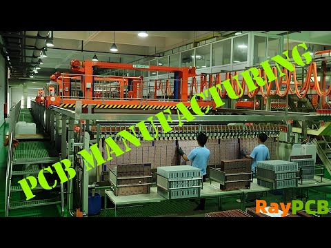
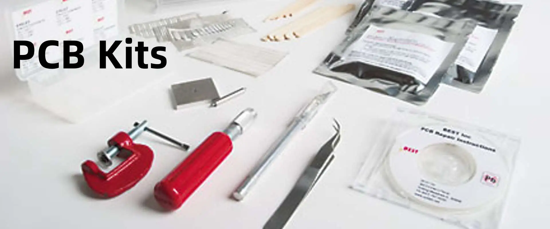
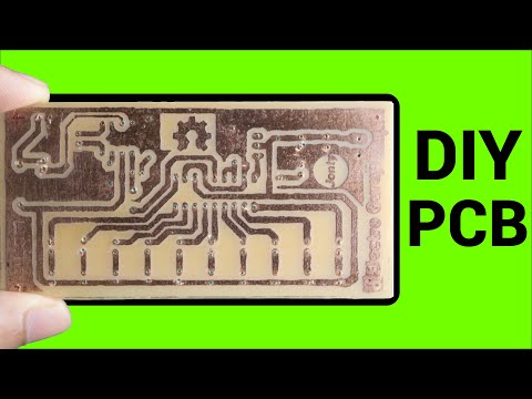
Printed circuit boards (PCBs) form the backbone of all electronic products and prototypes. Etching circuit layouts on copper clad boards is a critical first step in PCB fabrication. While small-scale commercial PCB production works for simple boards, it can get expensive for frequent iteration during product development stages. This is where a homemade PCB etching machine comes handy for rapid in-house prototyping.

This article provides step-by-step guidance on building your own DIY etching equipment with easily available components. We cover the complete instructions from the etching process basics, identifying materials needed, construction methods and tips for optimal results.

How PCB Etching Works

Before we jump into constructing the etching setup, let us understand the mechanics of copper etching.

The etching process removes unwanted copper from a copper clad laminate board to leave behind the intended conductive pattern – something similar to developing photographs. The key aspects are:

  • Printed circuit board with copper layer on substrate
  • Etching solution dissolves copper
  • Etchant-resistant protective layer on areas not to be etched

So the PCB sample is immersed into the etching solution which eats away copper without a protective mask. The masked areas emerge with copper traces in the desired circuit layout after etching and mask removal.

The DIY etching machine automates the immersion, agitation and rinsing steps while maintaining proper etchant characteristics.

Now let us look at choosing the right materials before designing the etching system.

YouTube video

Materials Selection

To build a functioning PCB etching setup, we need to select:

  • An enclosure tank
  • Etching solution
  • Agitation method
  • Heating approach
  • Plumbing fittings

Let us go through the options for each category and criteria for selection:

Enclosure Tank

This container holds the etching solution and the PCBs undergoing etching.

Ideal attributes are:

  • Acid-resistant material
  • Adequate size for PCB samples
  • Accessible for placing boards
  • Ports for fittings
  • Solution level markings

Suitable materials are glass, stainless steel & chemical-resistant plastics like HDPE, PP, PVC, PVDF. Avoid using aluminum.

5-10 liter tanks are common for DIY machines allowing 150×100 mm PCBs. Rectangular shapes provide a compact footprint. Ensure minimum two ports for fluid connections.

Etching Solutions

We need an etchant that can efficiently dissolve copper without harming the base laminate board. Common PCB etchants are:

Etchant Composition Characteristics
Ferric Chloride FeCl3 solution Fast acting, reusable
Ammonium Persulfate (NH4)2S2O8 + H2O Slower, single use
Sodium Persulfate Na2S2O8 + H2O Like ammonium, oxidizer
Hydrogen Peroxide + Acid H2O2 + HCl / H2SO4 Faster rate, high quality

Ferric chloride is the most popular for home etching given its rapid cu dissolution, reuse capability and easier handling than acidic mixtures. Prepare 30-45 degC, 1.5 litre FeCl3 stock solution at 35-45 gpl concentration.

Always exercise caution when preparing and using chemical etchants based on safety instructions.

Agitation Method

Agitation circulates the etchant uniformly across all surfaces of the PCB for smooth uniform etching without any sticking residues. Options are:

  • External pump recirculation
  • Air injection bubbles
  • Motorized paddle stirring

Small submersible pumps with 100 LPH (litres/hour) flow rate provide adequate circulation for DIY machines. Fit with PVC tubing allowing adjusted placement inside the tank.

Heating Approach

Heating the etchant accelerates the etching reaction rate. Considerations are:

  • Optimal temp is 30-45 degC for FeCl3
  • Direct heating risks fumes or reaction runaway
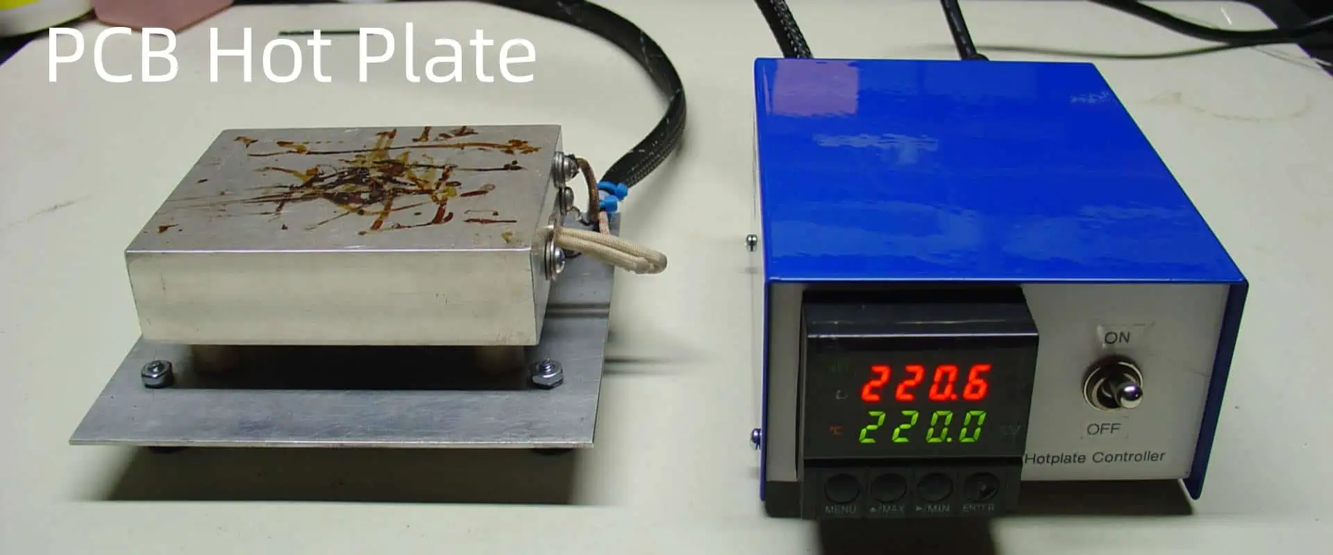
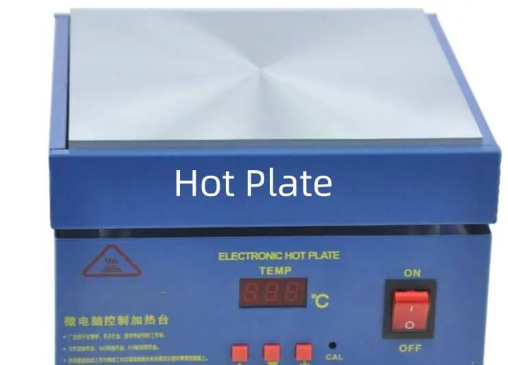
  • External heating with hotplate/element with thermal insulation

External heating of etching solution works safely using a hot plate or off-the-shelf brewing belt heater with thermal insulation wrapping. This maintains consistent solution temperatures.

Plumbing Fittings

We need suitable corrosion-resistant fittings and valves to enclose the fluid system enabling draining, refilling and filter cleaning operations.

  • Ball valvesย made of plastic/PVDF to control inlet, outlet and drain lines
  • Elbows & nipplesย – PP or PE construction
  • Liquid filterย – 10-20 micron filtration before pump inlet removes particulates

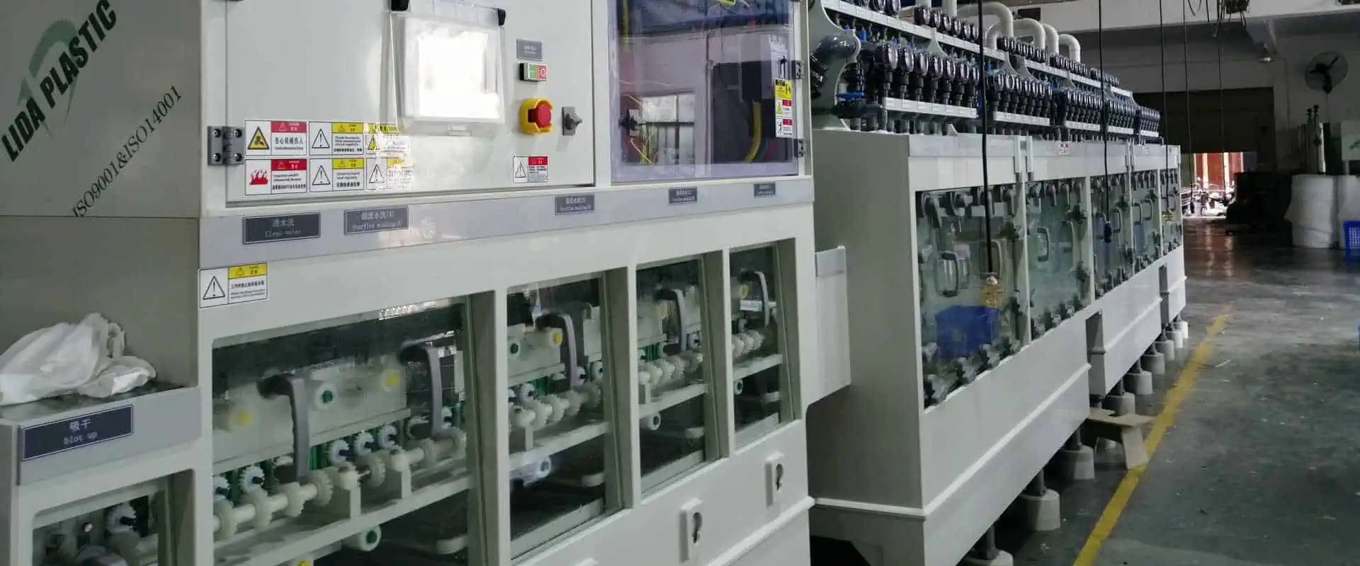
With the equipment criteria decided, let’s start the construction steps.

Constructing the Etching Machine

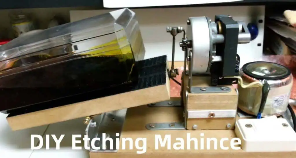
Follow these steps to build the complete etching unit:

1. Mark Container Lid Cutouts

The tank needs inlet and outlet connections for the heated etchant recirculation loop.

Cut out appropriately sized holes in the lid for:

  • Pump suction line
  • Return line from external heater
  • Drain outlet
  • Filter housing
  • Thermowell/temperature sensor
  • PCB holder access slot

Position to ensure free flow and also accommodate a false perforated bottom.

2. Assemble Fluid Plumbing Circuit

This forms the external heated recirculation loop for pumping etchant to and from the tank.

Connect the following hardware with solvent-welded joints:

  • PVC/PVDF valvesย on inlet, drain and return line
  • Elbows and nipplesย to match port alignments
  • Liquid filterย – install before pump inlet
  • External heaterย (hot plate/heating element) in the return line
  • Thermometer and sensor immersion wells/pockets with insulation

Insulate all heated areas to minimize heat losses. Place ball valves strategically to control flows.

3. Install Internal Agitation

This circulates heated etchant within the tank across all sides of the PCBs.

Fit a small fountain pump inside the tank through the inlet. Position it away from the PCB holder area with outlet oriented towards boards. This distributes fluids evenly ensuring no stagnant zones.

4. Set Drainage Mechanism

Provision for periodic draining and refilling of spent etchant.

Attach flexible chemical hose to the drain port valve reaching externally up to a storage bottle placed below tank level. This enables gravity drain by simply opening the valve.

Similarly connect the return line outlet into the etchant tank at adequate height. Place storage containers under drain outlet.

5. Enable Temperature Control

Maintaining optimum temperature accelerates etching without runoff issues.

  • Install thermowellย with sensor in tank inlet
  • Connect toย temperature controllerย unit
  • Use heating plate/coil with insulation as the control device

This regulates the external heater unit to heat circulating etchant fluid to preset 35-45 degC range.

6. Design PCB Holder

This cradles PCBs being etched evenly spaced from all sides allowing free flow of etchant.

Consider a perforated caddy with structural ribs or slotted panels. Anchor to the tank lid leaving the agitating pump area clear underneath.

Provision to mount PCBs vertically or horizontally facing the central fluid flow using snap-on clips or fasteners. Maximum panel size should match typical PCB blanks.

This completes construction of the etching equipment. Now we are ready to prepare the chemicals.

Preparing and Using the Etching Machine

Strip film etching line

Follow the start-to-finish sequence to use the etching system productively:

Step 1 – Prepare Ferric Chloride Etchant

Mix 1.5 litres of ferric chloride etchant stock solution in a separate container with deionized water. Concentration levels range from 35 grams per litre to 45 gpl depending on needed etching rates.

Always add the chemical to water gradually. Allow to fully dissolve using magnetic stirrer before transferring to the etching tank. Repeat until reaching max fill mark.

Step 2 – Test Heating System

Connect the heater and circulation plumbing to support external recirculation. Heat the etchant gradually to 35 degC temperature without connecting pump. Test insulation effectiveness.

Step 3 – Install Internal Pump

Secure the fountain pump inlet to tank lid cutout. Position outlet to face center of tank. Test check by running momentarily to prime all air bubbles and verify flow distribution.

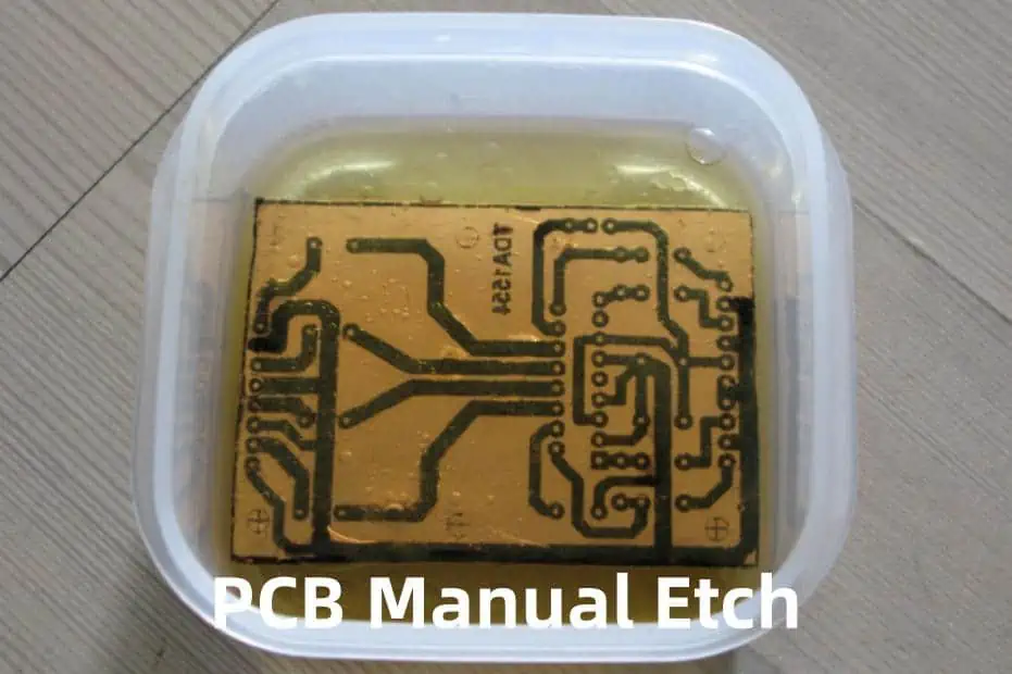
Step 4 – Load PCB Sample

Fabricate your printed circuit board layers with photoresist imaging of conductors ready for etching. This premasking protects areas not to be dissolved.

Hold PCB on the etching fixture and lower into fluid until halfway immersed with free flow to both sides.

Step 5 – Start Etching Run

Switch pump ON ensuring uniform bubblefree flow across panel surfaces. Maintain temperature at optimum 40 degC. Observe PCBs through tank lid till etching completes.

Step 6 – Drain, Rinse & Cleanup

Once all copper film dissolves, remove PCBs from tank and flush thoroughly with water spray. Drain back current batch of spent etchant into storage bottle for reuse.

Refill tank with preheated fresh etchant and repeat process for next PCBs. Check/replace fluid filter periodically.

This completes the operational workflow producing efficient etched printed circuit boards with your DIY machine.

Improving DIY Etcher Performance

Here are some tips to refine your homebrew PCB etching equipment:

  • Maintain consistent etchant characteristics like concentration and crystal level
  • Set optimal temperatures matching solution longevity
  • Regular filtration and carbon treatment to replenish etchant activity
  • Design suitable PCB holding fixtures optimizing area exposure
  • Uniform perforations on false tank bottom aiding bubble patterns
  • Judiciously use protective gear like face shield against splashes

Adhering to material compatibility, heating control and PPE guidance ensures safe experiential learning.

While basic DIY machines serve starter needs, you can enrich functionality like production grade etchers:

  • Automated temperature regulation loops
  • Microbubble generation for turbulence
  • Printed inner tank lining preventing wall adhesion
  • Spray wash stations using multiple etchant tanks
  • Programmable panel movement patterns
  • Used etchant regeneration systems

Creatively building your own etching equipment opens up affordable PCB prototyping capabilities encouraging electronics tinkering.

FAQ

Q1. Is a DIY etching machine safe for home use?

Yes, it is quite safe if elementary precautions around chemical handling, high temperature insulation and protective gear usage are followed. Certain etchants like ammonium persulfate are safer alternatives. Also lower concentration etchants take longer but minimize risks.

Q2. Can the same DIY etcher be used for etching aluminum boards?

No. PCB etchants like ferric chloride only dissolve copper without harming the fiberglass epoxy laminate boards. Aluminum requires aggressive caustic solutions which will also damage a DIY plastic tank system and needs special etcher materials.

Q3. How to store spent etchant solution from a homemade etching system?

Always drain used etchant gradually into sealable sturdy polyethylene bottles for safe storage. Allow sediments to settle at the bottom without agitation. Store containers properly labeled away from water contact and extreme temperatures. Reuse if suitable or professionally dispose based on regulations after sufficient neutralization.

Q4. What safety equipment should be used while operating my DIY etcher?

Use the following gear when operating the home etching setup:

  • Face shieldย – Protects face/eyes against splashes
  • Apronย – Prevents skin contact with chemicals through spills
  • Glovesย – Use thick nitrile outer gloves to cover hand completely
  • Fume maskย – Optional for filtering out irritant vapors

Also work in well ventilated outdoor/garage area.

Q5. How to dispose expired or excess ferric chloride etchant at home?

Never discard used etchant solutions directly into household drains. Allow it to crystallize in container and soak up sludge using paper towels for curing and drying. Wrap residue tightly with labels and call local waste management services for hazardous material disposal compliant to regional guidelines. Some metal recovery services also handle spent etchants responsibly.

What Is PCB FR4 Material Difference with FR1, FR2, FR3, FR5?

fr4 pcb

FR4 is the most widely used dielectric material in circuit board manufacturing, serving as the core substrate for single-sided, double-sided, and multi-layer PCBs. Its popularity stems from a combination of thermal stability, mechanical strength, and cost-effectivenessโ€”making it the default choice for most electronic applications. FR4 material has emerged as the industry standard, used in over 90% of rigid PCBs manufactured today. But what sets FR4 apart from its counterparts, and why has it become the go-to choice for PCB manufacturers?

This comprehensive guide will delve into the world of FR (Flame Retardant) materials, exploring the differences between FR4 and other grades (FR1, FR2, FR3, and FR5). We’ll examine their composition, properties, applications, and the reasons behind FR4’s dominance in the PCB industry.

Understanding Flame Retardant (FR) Ratings

Shengyi Autolad1 PCB

Before we dive into the specifics of each FR grade, it’s essential to understand what the FR designation means. The FR prefix refers to the flammability rating of the resin system used in the laminate composites that make up PCB substrates. These ratings are determined by standards set by organizations such as:

  1. UL 94 (Underwriters Laboratories)
    • Ratings range from V-0 (best) to V-2
  2. IEC 60695 (International Electrotechnical Commission)
    • Equivalent to UL 94 rankings

The addition of flame retardant compounds, typically bromine-based, to the resin produces self-extinguishing properties when the material is exposed to fire. This characteristic is crucial for ensuring the safety of electronic devices, especially in high-risk environments.

Read more about:

Overview of FR Material Grades

Let’s start with a brief overview of the different FR grades and their key characteristics:

  1. FR1: Basic phenolic resin with paper substrate
  2. FR2: Cotton paper phenolic
  3. FR3: Synthetic fiber epoxy
  4. FR4: Woven glass epoxy
  5. FR5: High Tg (glass transition temperature) woven glass epoxy

Each grade uses different combinations of base substrates and resin systems to achieve specific dielectric and flame retardant properties suitable for various electronics applications. Here’s a quick comparison of their capabilities:

MaterialDielectric ConstantLoss TangentTg ยฐCFlame Retardancy
FR14.5-6.00.04-0.05105-130Fair
FR24.8-5.20.03-0.05130-140Good
FR34.2-4.80.02-0.033140-170Better
FR44.3-4.80.02-0.027130-180Best
FR53.5-4.80.015-0.023>170Excellent

Now, let’s explore each FR grade in detail, focusing on their composition, characteristics, and applications.

FR1 Material: The Pioneer

FR1 represents the most basic form of flame-retardant PCB substrate, widely used in early consumer electronics.

Composition

  • Base: Paper
  • Resin: Phenolic

Characteristics

  • Dielectric Constant: Typically around 5 over RF/microwave bands
  • Loss Tangent: Approximately 0.05, indicating high signal loss
  • Tg: Maximum glass transition temperature of 130ยฐC
  • Flammability: Self-extinguishes, but not the fastest in flame suppression

Applications

While mostly obsolete today, FR1 served simple radio and pre-war telecommunications applications well. Its low cost made it suitable for basic electronic devices where performance requirements were not stringent.

Limitations

The high signal loss and low thermal rating of FR1 quickly became limiting factors as electronics evolved, leading to the development of improved substrates.

FR2 Material: A Step Forward

FR2 emerged in the 1950s-60s as an enhanced PCB substrate, utilizing cotton paper reinforced phenolic resin.

Composition

  • Base: Cotton paper
  • Resin: Phenolic

Characteristics

  • Dielectric Constant: Reduced to the 4.8-5 region
  • Loss Tangent: Similar to FR1, around 0.03-0.05
  • Tg: Up to 140ยฐC glass transition temperature
  • Flammability: Higher flame resistance compared to FR1

Applications

FR2 expanded PCB capabilities to meet the needs of industrial controls and instrumentation for aerospace applications during its era. While less common today, it’s still used in some niche low-frequency or high-temperature applications where electrical performance is less critical.

Advantages over FR1

The tightly woven cotton paper base provided improved thermal rating and mechanical stability compared to FR1, allowing for more diverse applications.

FR3 Material: The Glass Fiber Revolution

fr3 pcb

FR3 boards marked a significant advancement in PCB technology, introducing woven synthetic fiberglass mat embedded in epoxy resin.

Composition

  • Base: Woven fiberglass
  • Resin: Epoxy

Characteristics

  • Dielectric Constant: Dropped to the 4.2-4.8 range
  • Loss Tangent: Reduced as low as 0.02
  • Tg: Up to 170ยฐC temperature rating
  • Flammability: Significantly higher resistance compared to FR1 and FR2

Applications

FR3’s stable electrical properties enabled diverse applications, from oscilloscopes to missile guidance systems. While less common today, you may still encounter FR3 circuit boards in some legacy industrial electronics.

Advantages over FR1 and FR2

The woven glass base with improved synthetic resin allowed for increased component densities and high-speed signals that early PCB materials struggled with, paving the way for more complex electronic designs.

FR4 Material: The Industry Standard

FR4 represents the pinnacle of PCB substrate evolution, emerging in the 1970s with its optimal balance of capabilities.

Composition

  • Base: Woven fiberglass
  • Resin: Brominated epoxy (tetrabromobisphenol-A)

Characteristics

  • Dielectric Constant: Well-controlled at 4.4 ยฑ 0.2 across RF spectrum
  • Loss Tangent: Ranges from 0.018 down to 0.009 (low loss)
  • Tg: 130-180ยฐC typical glass transition temperature
  • Flammability: V-0 self-extinguishing in seconds

Why FR4 Dominates the PCB Industry

FR4 has become the universal choice for electronics over the past decades, accounting for over 90% of all PCBs manufactured. Here’s why:

  1. Electrical Properties
    • Extremely consistent dielectric constant across the RF spectrum
    • Low loss tangent, preserving high-frequency signals
    • Excellent insulation resistance (high Gฮฉ) at varied humidity/temperature
    • Withstands potting and conformal coatings well
  2. Physical Strength
    • High flexural strength, enduring mechanical stress
    • Resilience to fracturing from vibration/shock exposure
    • Good Z-axis compliance for multilayer boards
  3. Thermal Capabilities
    • 130ยฐC to 180ยฐC glass transition rating variants available
    • Many formulas withstand over 260ยฐC short term
    • Low CTE (Coefficient of Thermal Expansion) for thermomechanical stability
  4. Flammability Safety
    • High bromine content rapidly self-extinguishes burning
    • Passes UL94 V-0 3X at 0.75mm+ thickness
  5. Versatility
    • Suitable for a wide range of applications, from consumer electronics to aerospace
    • Available in various grades to meet specific requirements

FR4 Material Variants

The versatility of FR4 has led to the development of numerous variants, each tailored to specific applications:

  1. Standard FR4: General purpose PCBs
  2. High Tg FR4: Modified resin for 130ยฐC+ rating, suitable for industrial/military boards
  3. RF-35: Tightly controlled dielectrics for microwave/radio circuits
  4. FR408HR: High resin content for improved drilling and multilayer vias
  5. Getek: Woven and non-woven glass for high frequency/data boards
  6. CEM-1: Bismalemide triazine resin for extreme temperature aerospace applications
  7. Polyimide Blends: Mixed PI/epoxy resins for flexible circuits

FR5 Material: Pushing the Boundaries

fr5 pcb

FR5 represents the next step in high-performance PCB substrates, offering even better thermal and electrical properties than FR4.

Composition

  • Base: Woven fiberglass
  • Resin: High Tg epoxy

Characteristics

  • Dielectric Constant: 3.5-4.8, offering more flexibility for high-frequency applications
  • Loss Tangent: 0.015-0.023, lower than FR4 for improved signal integrity
  • Tg: >170ยฐC, providing excellent thermal stability
  • Flammability: Excellent flame resistance

Applications

FR5 is particularly suitable for high-speed digital circuits, aerospace, and military applications where extreme temperature resistance and signal integrity are crucial.

Advantages over FR4

  • Higher glass transition temperature, allowing for better performance in high-temperature environments
  • Lower loss tangent, enabling better high-frequency performance
  • Improved dimensional stability under thermal stress

Comparing FR4 with Other FR Grades

fr4 kb board

To fully appreciate the advantages of FR4, let’s compare it directly with the other FR grades:

FR4 vs. FR1

  • FR4 offers significantly better electrical properties, with lower signal loss and better consistency across frequencies
  • FR4 has superior thermal and mechanical properties, making it suitable for a wider range of applications
  • FR4 provides better flame retardancy, meeting stricter safety standards

FR4 vs. FR2

  • FR4’s woven fiberglass base provides better mechanical strength and thermal stability compared to FR2’s cotton paper base
  • FR4 offers lower signal loss and better high-frequency performance
  • FR4 has a higher glass transition temperature, allowing for use in more demanding thermal environments

FR4 vs. FR3

  • While both use fiberglass bases, FR4’s brominated epoxy resin provides better flame retardancy
  • FR4 generally offers better electrical properties, particularly in terms of loss tangent
  • FR4 has become more cost-effective due to its widespread adoption and optimized manufacturing processes

FR4 vs. FR5

  • FR5 offers higher glass transition temperatures, making it suitable for more extreme thermal environments
  • FR5 generally has lower loss tangent, potentially offering better high-frequency performance
  • FR4 remains more cost-effective and widely available for most applications, making it the preferred choice unless FR5’s specific advantages are required

Trends in FR4 Technology

Despite being the industry standard, FR4 material continues to evolve to meet the changing demands of modern electronics:

  1. Decreased Loss Tangents: Advanced formulations like RF-58 achieve loss tangents under 0.005, enabling higher frequency microwave boards
  2. Improved Processing: Optimized heat ramps during curing and laminating allow for drilling of increasingly thicker and thinner boards with fewer defects
  3. Higher Glass Transition Temperatures: Modified resin chemistry yields FR4 laminates with over 200ยฐC Tg, withstanding lead-free soldering and extensive thermal cycling
  4. Enhanced Dimensional Stability: Prepregs with balanced bi-directional weaves and fills attain near-zero CTE for precision analog sensing and advanced semiconductor packages
  5. Integrated Shielding: Mixtures of nickel, carbon, and silicon carbide fillers into base resins provide electromagnetic isolation right inside FR4 layers

Selecting the Right FR Material for Your PCB

When choosing between FR4 and other FR grades for your PCB design, consider the following factors:

  1. Application Requirements: Analyze signal frequency, noise susceptibility, conductor spacing, layer count, and embedded components
  2. Operating Environment: Consider temperature extremes, moisture exposure, mechanical stresses, and potential radiation exposure
  3. Regulatory Compliance: Ensure the chosen material meets relevant industry standards and certifications
  4. Cost Considerations: Balance performance requirements with budget constraints, considering both material costs and long-term reliability
  5. Manufacturability: Consult with your PCB fabricator about their capabilities and experience with different FR materials

Conclusion: The Enduring Dominance of FR4

FR4 material has earned its place as the backbone of the PCB industry through its balanced combination of electrical, thermal, and mechanical properties. While FR1, FR2, and FR3 paved the way for PCB evolution, and FR5 pushes the boundaries for extreme applications, FR4 remains the optimal choice for the vast majority of electronic designs.

The ongoing innovation in FR4 formulations ensures that this versatile material continues to meet the evolving needs of the electronics industry. From consumer devices to aerospace applications, FR4’s adaptability, performance, and cost-effectiveness make it the preferred substrate for PCB designers and manufacturers worldwide.

As technology advances, we can expect to see further refinements in FR4 technology, potentially expanding its capabilities to cover an even broader range of applications. While specialized materials like FR5 will continue to serve niche high-performance needs, FR4’s position as the industry standard remains secure for the foreseeable future.

By understanding the differences between FR4 and other FR grades, engineers and designers can make informed decisions, selecting the most appropriate material for their specific PCB requirements. Whether prioritizing signal integrity, thermal performance, or cost-effectiveness, FR4 and its variants offer a solution for nearly every electronic application, cementing its status as the cornerstone of modern PCB manufacturing.

How To Design PCB Guard Ring Properly

What is a Guard Ring?

A guard ring refers to a ring of traces routed around the perimeter of sensitive circuits on a printed circuit board. Guard rings act as a physical barrier to protect sensitive nodes against external interference or leakage currents.

Well-designed guard traces divert stray signals away from critical nodes, enhance electromagnetic compatibility, improve measurement accuracy, and prevent errant coupling into internal circuitry. Implementing effective guard rings is crucial when dealing with low-current sensing, high impedance, RF components, or circuits measuring small analog signals.

This article provides a comprehensive guide to implementing proper PCB guard rings, covering:

  • Guard Ring Principles and Layout
  • Connections and Routing
  • Optimizing Trace Widths
  • Guard Islands
  • Minimizing Leakage
  • Examples and Applications

Follow these best practices outlined below to add guard rings that reliably improve circuit performance in your next board design.

Guard Ring Design Principles

Before detailing guard ring implementation, we should review the key principles that make them work:

Electrostatic Protection

  • Guard traces form a Faraday cage, blocking electric field interference from coupling onto sensitive traces.

Shunting Stray Current

  • Any stray leakage gets shunted by the low impedance guard traces to ground.

Smaller Potentials

  • The guarded signal sees much less potential difference from the guard than external interference sources.

Keeping these mechanisms in mind will inform optimum guard layout and routing decisions when protecting critical nodes.

Layout Considerations

The first step in adding a guard ring is planning the trace layout around the protected component or circuit region.

Enclosing Sensitive Nodes

The guard trace should completely enclose the sensitive traces in a contiguous ring around the guarded circuit. Any gaps in coverage create openings for external signals to penetrate.

Following Component Contours

For guarding a specific IC or connector footprint, the ring should closely follow the outline of the component on all sides:

This ensures no exposed areas for leakage or coupling under the component.

Minimizing Openings

For board regions with dense routing, make the guard ring trace spacing and width match adjacent trace spacing to avoid openings between signals:

This helps divert stray signals across to ground better.

By thoughtfully arranging guard rings around components and signals, you can provide robust protection.

Guard Ring Routing

In addition to layout, connecting guard rings properly is also key for performance.

Single Point Grounding

The guard trace should only connect to ground at one location. Having multiple ground points allows currents to flow through the guard itself, reducing its effectiveness.

Dedicated Guard Layer

When possible, route guard traces on their own internal board layer. This prevents coupling between guard and sensitive traces.

Encircling Traces

Route guard traces to fully encircle protected signals on their layer. Sandwiching in plane layers provides further shielding.

Wide Traces

Make guard traces as wide as space allows. Increased area and lower resistance shunts more of any stray leakage through the guard.

Avoid Gaps or Branches

Guard traces should be continuous rectangles with no gaps or branches. This prevents leakage currents from jumping past the guard.

By incorporating these routing practices, your guard rings keep noise out of critical nodes.

Optimizing Guard Trace Widths

Determining the ideal guard trace width is an important consideration during layout. Wider traces enhance guarding performance but consume more space.

As a general rule of thumb, size guard trace widths equal to:

2-3x the width of the protected trace

So for safeguarding a 0.2mm analog signal:

  • Guard trace width = 0.4mm to 0.6mm

This provides good current shunting capability without oversizing.

For lower impedance guarding, the 5W:1G rule sets the width ratio between:

  • W = Protected signal trace width
  • G = Guard trace width

So surrounding a 0.2mm signal requires a 1.0mm guard trace. This provides more robust shielding for critical high-speed or RF traces.

Determine what level guarding your application needs and set widths appropriately. Dense boards may require balancing protection versus routing space.

Adding Guard Ring Islands

When laying out guard rings for circuits with multiple sensitive nodes, it helps to connect independent guard traces together into a larger guard island.

This offers several advantages:

Larger Shunt Area

  • Island combines area of all guards
  • Diverts more stray current

Simplifies Routing

  • Easier connecting one island than multiple rings

Robustness

  • Eliminates gaps that weaker lines can penetrate

Here is an example guard island safeguarding multiple op amps and ADC channels:

Note how the island surrounds all sensitive components and fills open areas in the layout.

Islands just need a single connection point to ground to avoid circulating currents.

Minimizing Guard Leakage

In precision measurement applications, even tiny leakage currents (picoamps) through the guard can impact accuracy.

Several techniques help reduce guard leakage:

Maximize Distance

  • Increase spacing between guard and sensed signals
  • Reduces capacitive coupling

Layer Separation

  • Sandwich guard trace between plane layers
  • Prevents traces from leaking

Independent Grounds

  • Use separate ground returns for guard and protected circuit
  • Avoids return path currents

Low Resistance

  • Ensure robust grounding and supply power to guards
  • Minimizes potential differences

With careful layout considerations, guard rings add minimal loading to precision circuits guarded.

Example Applications

Guard rings provide vital protection for:

Analog Sensing

  • Guards stop power supply noise from coupling into microvolt sensors

Radio Circuits

  • Prevent signals leaking between mixer/VCO stages

Voltage References

  • Shield 1.2V bandgap voltage from other supplies

High Impedance Nodes

  • Keep Gฮฉ input impedances isolated

EMI Sensitive Traces

  • Reduce emissions/susceptibility

And many more use cases – guard rings universally enhance circuit stability and precision.

FAQ

Here are some frequently asked questions on guard ring design and implementation:

Q: Does the quality of grounding impact guard ring effectiveness?

Yes. Any noise or shifting on the ground carries through to the guard ring since traces all connect eventually at a ground node. Properly designed low-noise ground planes ensure stable guard grounds.

Q: Can more than one guard ring enclose a signal?

Stacking multiple guard rings (on different layers) surrounding a trace enhances protection. However, each interconnected ring needs just one ground point to prevent circulation currents. Too many guards waste board space.

Q: Do components like resistors/caps placed inside guard rings get shielded too?

Unfortunately no. The guard ring effectively โ€œhidesโ€ the protected traces electromagnetically. But placed components donโ€™t experience the same shielding since they physically and electrically connect outside the guard boundary.

Q: Can guard rings be added around boards and board sections too?

Definitely. You will often see a row of ground vias routed around the very edge of boards acting as an outer guard boundary to contain EM fields inside. The same principle applies to shielding functional blocks by routing grounded copper regions between circuits across the board.

Q: What are acceptable breaks in guard rings around cutouts?

For necessary cutouts (connectors/holes etc.) the guard ring should continue symmetrically on all sides. Allowing small 5-10 mil gaps for drilling tolerances wonโ€™t severely degrade performance. But avoid routing signals through gaps if possible.

Conclusion

Implementing well-designed PCB guard rings enables robust, interference-free performance for sensitive circuits and precision boards. Following guard ring best practices for layout, routing, grounding and dimensions allows you to effectively shield critical signals from external noise sources and internal leakage. Give your low-level analog sensing, RF, and high-impedance circuits the isolation they deserve by guarding them with a ring of protection.

How i made a Wearable Heater from a PCB

As an engineer and hobbyist, I was looking for a way to create a wearable personal heater that could provide warmth on demand, using my skills in PCB design and electronic circuits. This article details my journey in designing and building a flexible printed circuit board (PCB) heater that can be worn.

Making a wearable heater from a custom PCB provides several advantages:

  • Thin and lightweight for wearing comfort
  • Flexible to wrap around different body parts
  • Customizable shape and size
  • Precise temperature control

I took inspiration from DIY sous vide immersion heaters and flexible PCB circuits used in wearables. By combining these concepts, I created a battery-powered heated garment perfect for keeping warm during winter outdoor activities.

Throughout this article, I cover:

  • Heater design considerations
  • PCB layout and fabrication
  • Component selection and testing
  • Construction of the wearable heater
  • Results for temperature performance
  • Lessons learned

Whether you want to replicate my project or design your own unique wearable heater, let the journey begin!

YouTube video

Design Considerations and Requirements

When embarking on engineering a flexible PCB heater, there were several important factors I needed to define:

Operating Parameters:

  • Supply voltage: 5V USB power bank
  • Temperature range: 100-115ยฐF (38-46ยฐC)
  • Target power density: 10 W per sq. inch

Physical Attributes:

  • Max size: 6 x 5 inches
  • Thickness: < 1mm with insulation
  • Flexibility: Wrap around limb
  • Water resistant insulation

Safety:

  • UL certified PCB material
  • Overheat shutdown circuit
  • Waterproof casing
  • Low voltage operation

Functionality:

  • Adjustable temperature setpoint
  • Independent control zones
  • Simple user interface

With these goals and constraints in mind, I could start developing the heater circuit design and PCB layout.

PCB Heater Design

The core mechanism behind the wearable heater is using thin copper traces on a flexible PCB as resistive heating elements. By passing current through the traces, they heat up according to:

Power (Watts) = Current^2 (Amps) x Resistance (Ohms)

To generate the 10 W/sq. inch target power density, I needed the right combination of trace width, thickness, and resistivity.

Heater Traces Layout

I designed a serpentine pattern of traces in two identical zones, allowing dual zone heating control:<table> <tr> <td>

To maximize heat output within the surface area, each zone contains long, winding traces with minimal spacing between them.

Key dimensions for the traces:

  • Trace width: 0.5 mm
  • Trace thickness: 1 oz (35 ฮผm) copper foil
  • Trace length: 15 inches per zone
  • Trace separation: 0.3mm

Calculating Necessary Trace Resistance

Using standard resistivity equations and values for 1 oz. copper PCB foil, I calculated the resistance required per zone:

To achieve about 10ฮฉ resistance in each zone, the long, thin traces I designed should work perfectly.

Now to select the proper electronic components for powering and controlling the heaters.

Electronic Circuit Design

With the PCB heating elements defined, I next created the schematic to power and control them. Key components include:

Power Supply

  • 5V Boost Converter: Efficiently boosts a USB power bankโ€™s 3.7V input up to 5V output.

Control Unit

  • Microcontroller Board: I used an Adafruit Feather with ATmega328P MCU and prototyping space.
  • MOSFET Switches: Use IRF520 high current MOSFETs to switch zone power.
  • Temperature Sensor: Provides local feedback for closed loop control.
  • OLED UI: Simple interface using only 3 buttons.

Safety Circuits

  • Resettable Fuse: Opens if overcurrent draw is detected
  • Crowbar Circuit: Handles overvoltage from power supply
  • Watchdog Timer: Auto shutdown if any faults occur in firmware

With dual MOSFETS independently controlling the zones, the microcontroller can maintain precise temperatures by using PID control and PWM. The cutoff fuse and crowbar provide protection from overloads, keeping things safe.

Now to lay out the circuit into a prototype PCB…

Prototyping the Heater PCB

To fabricate the initial heater PCB prototype, I used OSH Parkโ€™s flexible circuit board service. This allowed testing the design before investing in an expensive production flexible PCB run.

Here is how the four layer PCB stackup looked:

The empty mid layers act as power distribution planes once I etched openings for connectivity. The thin dielectric foam layers provide insulation between conducting layers.

I iterated through several prototype boards, adjusting the layout as needed to fit components and route traces.

After stuffing both heater zones with components, the final populated prototype looked like:

With the electronics complete, it was time to test out the heating performance…

Heater Testing and Results

I conducted several tests to characterize the thermal output of the prototype heaters:

Output Temperature Range

  • Applied different voltage levels to vary heating power
  • Measured steady state temperatures using thermocouple probe
  • Achieved range from 100 ยฐF to 140 ยฐF (38 ยฐC to 60 ยฐC)

Temperature Distribution

  • Used thermal camera to map surface temperatures
  • Center area runs hotter than edges -Difference of ~10ยฐF between hot spot and perimeter

Transient Heat Up Time

  • Heating from room temperature to 115ยฐF
  • Reaches 90% temp within 90 seconds

The figures matched well with my initial calculations and simulations for the custom heater traces. After several rounds of testing, I was satisfied with the thermal performance and ready to complete the full heated garment.

Constructing the Heated Garment

With a fully functioning flexible PCB heater, I could assemble it into a comfortable, wearable heated jacket insert by following these steps:

Step 1: Laminate Heater PCB

I coated both sides of the finished heater PCB with a thin layer of silicone conformal coating to provide electrical insulation and water resistance.

Step 2: Cut Fabric Layers

I cut rectangular pieces of fabric to sandwich around the PCB:

  • Outer fabric shell
  • Insulating foam layer
  • Soft inner liner fabric (against skin)

Step 3: Attach Hook and Loop Tape

I added small pieces of Velcro fabric tape to form an adjustable loop around an arm or leg when wrapped.

Step 4: Assemble Layers

I used a sewing machine to assemble all fabric layers together, with the PCB heater sealed inside and contact wires brought out.

Step 5: Attach Wiring and Controller

I connected heater wires to the control PCB board and sealed it inside a small project box for adjusting settings.

And there you have it โ€“ a flexible, wearable heater powered by a PCB and controlled by an Arduino!

Performance and Lessons Learned

Once assembled into wearable inserts, I found the flexible PCB heaters performed very well:

  • Quickly reaches 115ยฐF temp (sustained)
  • Conforms nicely to shape limb underneath
  • Thin and lightweight construction
  • No hotspots detected during use
  • Battery powers for ~3 hours per charge

However, I noted a few improvement opportunities for future revisions:

  • Use thicker copper and polyimide layer to increase power density
  • Improve outer insulation; some water penetration when sweating
  • Optimize battery selection for longer run times
  • Add Bluetooth for wireless control

Overall though, given the basic tools and resources I used, Iโ€™m thrilled with how my flexible PCB wearable heater came out! It provides the perfect amount of personal heating for helping me stay warm in the winter.

And since the PCB design files are fully shared, you can build your own or even improve on my original design. Just let me know what version 2 of this DIY heated garment looks like!

FAQ

Here are some common questions on building your own PCB-based wearable heater:

Q: What PCB thickness should be used for flexibility?

A: A 4-layer board up to 0.8mm thick works well. The thin dielectric layers enable the entire board to bend and fold easily.

Q: What temperature range can a PCB heater reach?

A: With careful design, you can achieve consistent surface temperatures from 100ยฐF to over 200ยฐF if needed. But higher heat requires thicker copper and better insulation.

Q: Is sealed conformal coating enough insulation for skin contact?

A: For direct skin contact, I recommend laminating fabric insulation layers around the cured PCB for safety and comfort. Silicone coats alone may not provide enough protection long term.

Q: How long can these heaters run on batteries?

A: Battery life depends on heating power needs and battery capacity used. With 5000 mAh USB power banks, I achieved 2 to 4 hours of runtime while drawing around 5-10W total. Adding multiple banks can extend operation further.

Q: What safety concerns exist around DIY PCB heaters?

A: Be sure to properly insulate all traces and high voltage sections. Include fusing, over-temperature monitoring, and redundant physical shutoffs. Never leave powered unattended. Carefully test insulation prior to wearing. Consider low voltage supplies to limit risks.

Conclusion

I had tremendous fun engineering flexible PCBs into wearable heaters for the first time. The circuit design, layout techniques, prototyping iterations, and insulation methods I devised provide a solid starting point for this emerging project area. While DIY electrical garments require great care in safety and testing before regular use, the personalization and customization possible makes it an exciting field ripe for innovation. I welcome you to take inspiration from my heated garment design files and see how you can push wearable PCB tech further with your own creative spin!

How Do You Use a PCB Hot Plate for SMD soldering?

A hot plate comprises an electronically heated platform allowing precision temperature control up to 300ยฐC necessary for print circuit board (PCB) surface mount device (SMD) soldering processes including baking, reflow or rework station preheating. Hot plates assist solder paste curing before component placement as well as post-assembly lead-free solder reflow.

This article details hot plate usage methodologies during PCB SMD population focusing on appropriate SMD sizing, ideal placement locations, optimal heating techniques, process tuning considerations and maintenance best practices when employing programmable hot plate systems to fully leverage their capabilities improving solder joint integrity necessary for reliable electronics functionality across myriad end-use conditions.

YouTube video

Working Principle of PCB Hot Plates

Hot plate systems consist of:

  • Ceramic Heating Platform โ€“ Flat thermally conductive top supporting PCBs
  • Temperature Controller โ€“ Closed loop precision heating element energizer
  • Insulated Housing โ€“ Bottom covers minimizing heat losses
  • Adjustable Stand โ€“ Raises hot plate to comfortable height

A sensor feedback loop allows the controller to regulate heating elements embedded underneath the ceramic top achieving exceptionally uniform and stable temperature setpoints within +/- 2ยฐC. Some models even incorporate vacuum holders firmly securing boards during reflow/rework.

Key Hot Plate Specifications

  • Temperature Range โ€“ At least 150ยฐC covers most hand soldering applications
  • Plate Size โ€“ Dimensions suiting largest PCBs needing heating
  • Control Stability โ€“ +/- 2ยฐC for repeatable process consistency
  • Heating Rate โ€“ Up to 10ยฐC/sec facilitates rapid reflow when hand soldering
  • Vacuum Strength โ€“ Prevents thin/warped boards lifting during reflow
  • Programmability โ€“ Microcontroller regulation allows tuning thermal profiles
  • Independent Zones โ€“ Separate areas preventing localized hotspots

Why PCB Hot Plates Aid Soldering

During hand soldering, applying localized heat only to soldering iron contact points risks temperature gradients across large boards preventing simultaneous reflow when attaching multiple components.

Hot plates provide whole area bottom side heating enabling even preheating facilitating concurrent top side iron solder melting together minimizing deltas preventing cracked joints from board warping arising due to non-uniform thermal expansion.

Precision closed loop thermal regulation also aids solder paste curing, moisture baking or component rework needing consistent heating unattainable using hand-held heat guns. Thereby hot plates simplify achieving process repeatability necessary for quality soldering.

PCB Component Sizing Considerations

Judicious component selection and placement proves vital when hot plate soldering:

  • Avoid Large Metal-Cased Parts โ€“ Significant thermal mass demands more heat input slowing process
  • Select Small Surface-Mount Packages โ€“ Chips, 0402/0603 passives minimize reflow duration
  • Use Low Temperature Solders โ€“ Sn42/Bi58 melts faster than lead-free alloys
  • Place Devices Centrally โ€“ Eliminates positioning beyond heated boundaries

Grouping similarly sized SMD parts together also aids batch soldering instead individually processing each element. However balancing these layout considerations against electrical performance needs and routing congestion challenges persists key for complex boards.

Solder Paste Selection

When stenciling paste for hot plate reflow, consider:

  • Smaller Pitch Devices โ€“ Type 3 powder sizes limit solder balling risks
  • Thermal Demands โ€“ High conductance paste assists heat transfer
  • Alloy Compatibility โ€“ Matching paste melting points with solder types
  • Flux Requirements โ€“ Appropriate activity levels for difficult metals
  • Curing Needs โ€“ Snap cure pastes speed up heating stages

Thereby understanding solder material interfacial combinations proves vital when vetting options.

PCB Hot Plate Usage Methodology

Follow these steps when employing hot plates during soldering:

Phase 1 – Temperature Profiling

  • Adjust controller to span 60-250ยฐC for profiling
  • Affix thermocouples onto dummy PCB surface
  • Gradually ramp temperature while logging sensor readings
  • Determine settings achieving target degree/second rate

This provides the thermal response signature of boards for tuning reflow profiles.

Phase 2 โ€“ Flux Application

  • Lightly wet a swab with rosin flux
  • Gently apply flux onto PCB pads avoiding migration
  • Keep flux amount minimal preventing char residue

Flux removes surface oxidation enabling solder wetting.

Phase 3 – Solder Paste Dispensing

  • Load stencil onto PCB and align aperture openings
  • Spread paste over stencil using a squeegee
  • Carefully detach stencil checking all pads
  • Touch-up missing spots using a syringe

Stenciling enables rapid precise paste deposition.

Phase 4 – Component Placement

  • Pick each part by the casing using tweezers
  • Locate component contacts evenly inside pads
  • Gently lower element allowing self-centering
  • Check alignments meet specifications

Precision positioning prevents tombstoning issues.

Phase 5 – Profiled Reflow

  • Keep board flat on heated surface
  • Set 30-70ยฐC above liquidus temperature
  • Gradually ramp up temperature
  • Hold peak once paste reflows then cool

This liquefies paste contacting leads forming reliable intermetallic solder joints post-solidification.

Phase 6 โ€“ Residual Flux Cleaning

  • Spray electronics-grade cleaner onto boards
  • Gently brush using ESD-safe swabs
  • Avoid forceful rubbing damaging bonded leads
  • Dry boards using low pressure ionized air

Removing activators/residues prevents electrical leakages across insulators.

Phase 7 โ€“ Inspection

  • Visually check solder fill within joint fillets
  • Verify no extraneous solder balls/spikes
  • Inspect for missing or misaligned connectors
  • Reheat/adjust elements failing criteria

Detailed examination validates robust attachments.

Reflow Profile Adjustments

Tune profile parameters only in small increments during initial runs while reviewing impacts to avoid overshoot:

Profile Duration โ€“ Lengthening overall duration increases time above liquidus enhancing joint wetting

Ramp Rate โ€“ Faster ramps achieve quicker reflow; but risks paste slumping

Peak Temperature โ€“ Higher settings reduce solder surface tension improving fill; but hurts components

Cooling Ramp โ€“ Slower cooling hardens joint microstructure; but risks grainy/dull finishes

Maintaining meticulous soldering logs while methodically varying single parameters during profiling provides the empirical process window necessary for optimizing programmable oven/hot plate routines needed achieving repeatable high-yield results.

Thermal Profile Data Logging

Use thermocouples for logging PCB heating during initial profiling:

  • Non-Contact InfraRed Thermometers โ€“ Rapidly scans board without soldering probes
  • Type-K Glass-Braid Thermocouples โ€“ Rated for over 200ยฐC measurements
  • Miniature Integrated Probes โ€“ Compact formats occupying less space
  • Flexible Wide Temperature Sensors โ€“ Conforms across uneven/warped boards
  • Multi-Channel Data Loggers โ€“ Logs entire oven thermal maps simultaneously

Profiling runs should cover several repeated cycles logging heating/cooling trends for identifying tuning opportunities to meet acceptable process windows.

Such empirical data then supplements oven vendor recommendations for computing optimized thermal routines matching board materials, components, form factors and throughput needs.

Hand Soldering Techniques

When hand soldering complexes boards under hot plates:

Apply Fluxes Judiciously โ€“ Use minimal amounts; remixed frequently

Keep Tips Clean โ€“ Replace/rewet dirty iron parts hindering heat transfers

Vigorously Stir Solder โ€“ Aggressively blend preventing precipitation

** Anchor Components Initially** โ€“ Fix parts using minimaliste solder avoiding movement

Shield Adjacent Parts โ€“ Attach heat sinks onto nearby temperature-sensitive devices

Use Low Power for Finesse โ€“ Reduce iron temperatures when dealing with delicate trims

Such seemingly trivial aids significantly improve reliability when hand working dense boards.

Reworking Defective Joints

Follow these steps when reworking faulty solder joints using hot plates:

Raise Board Temperature โ€“ Heat surrounding zone to reflow temperatures softening joint

Vacuum Hold Board โ€“ Prevent warping or lifting during manipulations

Remove Existing Solder โ€“ Use desoldering braid to absorb defective solder

Clean Terminations โ€“ Swab flux removing oxidation from revealed surfaces

Apply Fresh Solder โ€“ Use suitable gauge for reattaching freed component pins

Examine New Joint โ€“ Visually check realignments, confirm adequate fill

Strictly controlling temperatures allows safely detaching elements for adjustments or repairs avoiding collateral thermal damage.

Advanced Reflow Techniques

Certain applications utilize advanced hot plate assisted attachment options:

Vapor Phase Reflow โ€“ Boiling fluorinert films transfer latent heat for uniform heating

Photonic Reflow โ€“ Directed infrared beams selectively cure designated zones

Thermo-Compression Bonding โ€“ Forcefully pressing interconnects under heat fuses contacts

Transient Liquid Phase Bonding โ€“ Intermediate melting point metals aid joint formations

Electro-Magnetic Soldering โ€“ Alternating magnetic fields directly heat susceptors minimizing thermal transfers

Thereby hot plates simplify exploring such techniques across niche applications needing precise temperatures unattainable using handheld units.

Hot Plate Calibrations

Routine maintenance activities sustain long-term performance:

Thermocouple Recalibrations โ€“ Yearly sensor accuracy validation against certified references

Heating Element Replacements โ€“ Swapping aging heaters restores power delivery

Controller Firmware Updates โ€“ Latest software improves regulation capabilities

Gasket Inspections โ€“ Examine seals preventing external air leaks

Ceramic Tile Scrubbing โ€“ Eliminate carbon/flux buildup using solvents

Platform Flatness Checks โ€“ Assess warping needing mechanical adjustments

While requiring Planning schedule downtime, such actions ensure continuous optimum functionality.

Safety Precautions

Exercise abundant precautions when operating hot plates:

  • Mandate hand gloves avoiding accidental skin contacts
  • Confirm boards remain entirely on heated platform
  • Follow maximum temperature ratings for flammable boards
  • Cease operations upon seeing smoke possibly indicating scorched flux residues
  • Allow sufficient cooldown before handling recently energized unit

Such prudence minimizes workplace mishaps or equipment damage risks from operational excursions exceeding safety envelopes across inherently hazardous high-temperature processes.

Conclusion

This guide examined appropriate SMD selection factors, precise paste printing, controlled thermal profiling, data logging aids and safety protocols when employing benchtop hot plates for assisting hands-free bottom preheating delivering rapid yet gentle reflow necessary for reliable lead/lead-free PCB soldering โ€“ especially vital producing complex multilayer boards containing moisture sensitive components or high pin count fine pitch devices extremely vulnerable to thermomechanical fractures resulting from uncontrolled heating. Properly incorporating such feedback-controlled programmable platforms significantly enhances assembly repeatability even during low-volume prototype runs using hand soldering. The future potential of additive lateral heat sources for further optimizing board level heating distributions heralds even better soldering yield improvements necessary sustaining further PCB miniaturization trends.

Frequently Asked Questions

What is the advantage of a PCB hot plate over a reflow oven?

Key advantages hot plates offer over large convection ovens include tighter temperature uniformity across small boards via direct contact conduction, closed loop precision hardly achievable using blown heat, smaller form factors suitable for hand assembly stations, lower power saving energy plus faster thermal response attaining quick reflow ideal soldering heat-sensitive components.

What PCB surface finish works best for hot plate soldering?

Exposed PCB surface pad finishes using immersion silver or electrolytic hard gold demonstrate the best solderability for hot plate manual soldering applications given their oxidation resistance at elevated pre-heat temperatures compared to bare copper prone to surface dulling or HASL tin-lead layers tending to melt prematurely ahead of solder pastes preventing intermetallic alloying necessary for sound joints.

Are leaded or lead-free solders preferred for PCB hot plates?

Although leaded solders melt ~30ยฐC lower than lead-free alternatives thereby needing lower peak pre-heat temperatures, given tightening environmental legislation banning lead material usage plus lead-free alloys better resisting tin whiskering risks under temperature cycling necessary for automotive grade boards, lead-free SAC305 or SN100C formulations prove most widely adopted even for hand soldering using benchtop hot plate stations.

How flat must PCB boards be for hot plate soldering?

Ideally, boards should remain completely flat within under 2mm deflection across each linear dimension at peak preheat temperatures to prevent localized solder reflow simultaneously across pads caused by height differentials or air gaps exceeding thermal conduction capabilities of most hot plates having typical 150mm throat depths although advanced versions allow programmatically creating several independent heating zones targeting slightly warped multilayer boards.

How are temperature uniformity verified across PCB hot plates?

Checking hot plate pre-heat platform uniformity involves logging temperature readings using an orthogonal matrix of thermocouples spanning the heated top and then calculating deviation extremes across mapped area for determining necessary modifications either through controller tuning or by physically shimming the heated ceramic element improving flatness thereby attaining under 5ยฐC variance consider acceptable for SMD hot plate soldering applications without causing solder balling issues.

The Complete Guide to Controlled Impedance in PCBs: Design, Calculation, and Manufacturing

impedance control pcb

Today’s electronics demand increasingly compact, high-speed PCB designs where every trace and component interaction matters. As operating frequencies routinely reach GHz ranges and signal integrity becomes paramount, simple conductor connections no longer suffice.

Controlled impedance has emerged as a critical factor in PCB performance. Designers must now carefully analyze critical nets, trace geometries, and their board’s material properties to maintain signal quality. In high-speed digital and RF applications, proper impedance management isn’t just beneficial – it’s essential for reliable circuit operation.

What is Impedance Control PCB?

Impedance control PCB refers to the process of designing and manufacturing printed circuit boards with specific trace impedances. This technique ensures that the electrical characteristics of PCB traces remain consistent throughout the signal path, which is critical for maintaining signal integrity in high-speed and high-frequency applications.

Why is Impedance Control Important in PCB Design?

Impedance control PCB design is crucial for several reasons:

  1. Signal Integrity: It minimizes signal reflections and distortions, ensuring clean signal transmission.
  2. High-Speed Performance: Essential for devices operating at high frequencies or data rates.
  3. Electromagnetic Compatibility (EMC): Helps reduce electromagnetic interference (EMI) and improve overall system performance.
  4. Compliance: Many industry standards require specific impedance values for certain interfaces.
Controlled Impedance Calculator
RayPCB Engineering Tools
Ground Plane Dielectric (ฮตr) W Trace Width (W) H
Surface Microstrip Transmission Line
mm
mm
mm
ฮฉ Common: 50ฮฉ (single-ended), 90ฮฉ/100ฮฉ (differential)
ยฉ RayPCB Engineering Tools | Calculations are estimates only
Need Help? Contact RayPCB โ†’

Types of Controlled Impedance in PCBs

PCB Impedance

When discussing impedance control PCB design, it’s important to understand the different types of controlled impedance configurations:

Single-Ended Impedance

Single-ended impedance is the most common type in impedance control PCB design. It refers to the impedance of a single trace measured against a reference plane (usually ground). Typical values for single-ended impedance are 50ฮฉ or 75ฮฉ, depending on the application.

Differential Impedance

Differential impedance involves a pair of traces carrying complementary signals. The impedance is measured between these two traces. Differential pairs are commonly used in high-speed digital interfaces like USB, HDMI, and PCIe. Typical differential impedance values are 100ฮฉ or 120ฮฉ.

Coplanar Impedance

Coplanar impedance refers to traces on the same layer with ground planes on either side. This configuration is often used in RF and microwave circuits. The impedance in coplanar waveguides depends on the trace width, the gap between the trace and adjacent ground planes, and the dielectric properties of the substrate.

Lear more about:

Factors Affecting Impedance Control PCB Design

Several factors influence the impedance of PCB traces. Understanding these factors is crucial for effective impedance control PCB design:

1. Trace Geometry

The width and thickness of the trace significantly affect its impedance. Wider traces generally have lower impedance, while narrower traces have higher impedance.

2. Dielectric Material

The properties of the dielectric material, particularly its relative permittivity (ฮตr), play a crucial role in determining trace impedance.

3. Stackup Design

The arrangement of layers in the PCB, including the distance between signal layers and reference planes, impacts impedance.

4. Copper Weight

The thickness of the copper used for traces (often referred to as copper weight) affects both the trace’s resistance and its impedance.

5. Surface Finish

Different surface finishes can slightly alter the effective dimensions of the traces, impacting their impedance.

YouTube video

How to Calculate Impedance in PCB Design

Calculating impedance is a critical step in impedance control PCB design. While sophisticated software tools are available for precise calculations, understanding the basic formulas provides valuable insights:

Microstrip Impedance Calculation

For a microstrip (a trace on the outer layer with a ground plane beneath), the impedance can be approximated using:

Z0 = [87 / (โˆš(ฮตr + 1.41))] * ln(5.98h / (0.8w + t))

Where:

  • Z0 is the characteristic impedance
  • ฮตr is the relative permittivity of the substrate
  • h is the height of the trace above the ground plane
  • w is the width of the trace
  • t is the thickness of the trace

Stripline Impedance Calculation

For a stripline (a trace embedded between two ground planes), the impedance can be approximated using:

Z0 = [60 / โˆšฮตr] * ln[1.9b / (0.8w + t)]

Where:

  • b is the distance between the ground planes
  • Other variables are the same as in the microstrip formula

It’s important to note that these formulas are approximations. For precise impedance control PCB design, especially in high-speed or RF applications, it’s recommended to use specialized PCB design software or consult with PCB manufacturers.

Best Practices for Impedance Control PCB Design

Implementing effective impedance control PCB design requires attention to detail and adherence to best practices:

1. Maintain Consistent Trace Width

Keep trace widths consistent throughout the signal path to maintain uniform impedance.

2. Use Smooth Transitions

Avoid abrupt changes in trace direction. Use curved traces or 45-degree angles for turns.

3. Proper Stackup Design

Design your PCB stackup carefully, ensuring consistent reference planes for controlled impedance traces.

4. Mind the Return Path

Ensure a clear and uninterrupted return path for high-speed signals, typically on an adjacent layer.

5. Differential Pair Routing

For differential pairs, maintain tight coupling and equal length between the two traces.

6. Avoid Impedance Discontinuities

Minimize the use of vias in controlled impedance traces, as they can introduce impedance discontinuities.

7. Use Stitching Vias

When changing layers, use stitching vias near the transition to maintain a consistent return path.

Manufacturing Considerations for Impedance Control PCB

PCB trace impedance

Successful impedance control PCB manufacturing requires close collaboration between designers and manufacturers. Here are key considerations:

1. Material Selection

Choose appropriate PCB materials with consistent dielectric properties for reliable impedance control.

2. Copper Weight

Specify the correct copper weight, as it affects both trace impedance and manufacturability.

3. Tolerances

Understand and specify the required tolerances for trace width and spacing, as well as overall board thickness.

4. Testing and Verification

Implement proper testing procedures, such as Time Domain Reflectometry (TDR), to verify impedance values.

5. Documentation

Provide clear and detailed documentation of impedance requirements to your PCB manufacturer.

Measuring Impedance in Manufactured PCBs

Verifying the impedance of manufactured PCBs is crucial for quality control. Here are common methods for measuring impedance:

1. Time Domain Reflectometry (TDR)

TDR is the most common method for measuring PCB trace impedance. It sends a fast rise-time pulse down the trace and measures reflections caused by impedance discontinuities.

2. Vector Network Analyzer (VNA)

VNAs are powerful tools for measuring impedance, especially useful for RF and microwave circuits. They measure scattering parameters (S-parameters) of the trace, which can be used to calculate impedance.

3. Impedance Coupon Testing

Many PCB manufacturers offer impedance coupon testing as part of their quality control process. Test coupons with controlled impedance traces are included on the panel with the PCBs and measured using TDR or other methods.

Advanced Topics in Impedance Control PCB Design

As you delve deeper into impedance control PCB design, consider these advanced topics:

1. High-Speed Design Considerations

For high-speed designs, factors like skin effect and dielectric loss become increasingly important. These phenomena can affect signal integrity and must be accounted for in impedance calculations and overall PCB design.

2. Impedance Control in Flexible PCBs

Flexible and rigid-flex PCBs present unique challenges for impedance control. The bending of traces and varying dielectric properties in different areas of the board require special consideration.

3. Electromagnetic Simulation

Advanced electromagnetic simulation tools can provide detailed insights into signal behavior and impedance characteristics, allowing for more precise impedance control PCB design.

4. Embedded Passives and Impedance Control

The use of embedded passive components can impact impedance control. Understanding how to design and manufacture PCBs with embedded passives while maintaining controlled impedance is an advanced skill.

Troubleshooting Common Impedance Control PCB Issues

Even with careful design and manufacturing, impedance control PCB issues can arise. Here are some common problems and their solutions:

1. Impedance Mismatch

Symptom: Signal reflections and degraded signal quality. Solution: Verify trace widths, dielectric thicknesses, and material properties. Adjust design or manufacturing process as needed.

2. Crosstalk

Symptom: Interference between adjacent traces. Solution: Increase spacing between traces, use guard traces, or adjust layer stackup to improve isolation.

3. Inconsistent Impedance Along Trace Length

Symptom: Varying signal quality at different points along the trace. Solution: Ensure consistent trace width and reference plane integrity throughout the signal path.

4. Resonance Issues

Symptom: Signal integrity problems at specific frequencies. Solution: Analyze and adjust trace lengths to avoid creating unintentional resonant structures.

Future Trends in Impedance Control PCB Design

As technology continues to advance, impedance control PCB design is evolving to meet new challenges:

1. Higher Frequencies

With the advent of 5G and beyond, PCB designs must accommodate ever-higher frequencies, requiring more precise impedance control.

2. Miniaturization

As devices become smaller, maintaining controlled impedance in dense, compact layouts becomes more challenging.

3. New Materials

Development of new PCB materials with improved dielectric properties will offer new possibilities for impedance control in high-performance applications.

4. Artificial Intelligence in PCB Design

AI-assisted design tools are emerging, potentially revolutionizing how we approach impedance control PCB design and optimization.

Conclusion

Mastering impedance control PCB design is essential for creating high-performance electronic products in today’s fast-paced technological landscape. From understanding the basic principles to implementing advanced techniques, this guide has covered the critical aspects of controlled impedance in PCB design and manufacturing.

Remember, successful impedance control PCB design is not just about following rules and formulas. It requires a deep understanding of electromagnetic principles, close collaboration between designers and manufacturers, and a commitment to continuous learning and improvement.

As you apply these principles in your PCB projects, you’ll develop an intuition for impedance control that goes beyond mere calculations, leading to more robust and reliable electronic products. Whether you’re designing high-speed digital circuits, sensitive analog systems, or cutting-edge RF applications, mastering impedance control PCB design is an essential skill that will set your work apart in the ever-evolving field of electronics.

What Is the Best PCB Inspection Microscope ?

Printed circuit board (PCB) manufacturing involves stringent quality checks to validate fabrication accuracy before shipment. Visual inspection remains indispensable for verifying PCB layer alignment, pad geometries, soldermask tolerances, and confirming drill hole sizes across boards utilizing specialized inspection microscopes providing high quality imaging.

However, with ongoing PCB technology advancements enabling smaller line widths, tighter pitches and finer tolerances, traditional stereo optical microscopes prove inadequate necessitating more advanced magnification solutions.

This article outlines key considerations when selecting PCB inspection microscopes, examines popular models, and provides a feature comparison across different price categories to help identify the best value options.

YouTube video

Importance of Visual PCB Inspection

Automated optical inspection (AOI) systems employing sophisticated imaging techniques provide first-line quantitative dimensional analysis checking PCB panels for defects during fabrication. However, final quality assurance requires detailed physical verification against pertinent design specs.

Engineers perform various critical validations only possible through visual examinations under microscopes, including:

Trace Width Measurements โ€“ Confirming etched conductor widths match layout rules across different PCB routing layers

Pad Spacing Analysis โ€“ Verifying clearance tolerances between closely spaced pads or vias

Soldermask Inspection โ€“ Checking for complete paste coverage with no voids or scratches

Conductor Roughness โ€“ Detecting pits, nicks or inconsistent metal etch roughness along traces

Plating Integrity โ€“ Validating uniform copper, tin, silver or gold plating thickness on pads

Drilling Circularity โ€“ Assessing drill hole diameter consistency and edge roughness

Step-and-Repeat Accuracy โ€“ Measuring alignment marks validating pattern overlay precision

wegewVoiding โ€“ Detecting insufficient filler or air gaps around pads on soldermask or metal layers

Since these dimensional verifications require micron-level imaging resolutions, PCB designers need access to advanced magnification systems during final board bring-ups while avoiding cost overkill.

Types of PCB Inspection Microscopes

Several optical instrumentation solutions assist PCB analyses:

Stereo Microscopes

Stereo microscopes contain paired eye tubes with separate light paths providing slightly offset images recombined by the visual cortex into enhanced 3D depth perception without fish-eye distortion at lower 5-100x magnification ranges. Large working distances accommodate inspecting populated PCB assemblies. However, resolution proves inadequate assessing finer fab layers.

Compound Microscopes

Compound microscopes employ a two stage magnification system with initial 10-100x magnification from an objective lens followed by added 10-15x eyepiece zoom boosting overall viewing up to 1500x levels necessary for detail PCB analyses. High numerical aperture objectives enhance resolution but limit working distances. Mounted camera modules assist image capture across smaller fields of view during PCB examinations.

Digital Microscopes

These eliminate conventional eyepieces replacing optical tubes with high resolution CMOS/CCD imaging sensors providing magnification levels up to 300x when coupled to large HD displays. However, lower sensor pixel density restricts resolving capacity crucial for PCB work. Touchscreen manipulation conveniences standalone operation but subjects displays to contamination.

Measuring Microscopes

Measuring microscopes incorporate high precision linear encoded or rotary stages coupled to fine-adjustment focusing nosepieces providing micron-level X-Y positioning repeatability essential for dimensional metrology. Glass reticle overlays or software-based gridlines enable measuring key PCB features like conductor spacing, hole sizes or land widths. However bulk hampers manipulation flexibility.

Benchtop Microscopes

Benchtop models with boom stands keep main optical assembly base stationary while allowing adjustable slide stages or camera tubes to move facilitating inspection access across large PCBs with flexible side-on viewing. Extended working distances accommodate examining populated boards or instances needing auxiliary lenses attachment. High intensity ring lights assist surface illumination.

Key Specifications for PCB Inspection

Microscope selection factors include:

Magnification Range โ€“ 100x-500x levels necessary for tracing conductors or examining drill hole walls by resolving sub-25-micron features

Working Distance โ€“ At least 6 inches provides clearance inspecting dense bottom-side components on multilayer PCBs

Illumination โ€“ Ring lights with diffused LEDs prevent harsh reflections across copper layers

** resolving** โ€“ Diffraction-limited optics reduce aberration enhancing edge visibility

Field of View โ€“ Larger viewing facilitates quicker area scans during PCB analyses

Zoom Ratio โ€“ 10:1 or higher provides sufficient magnification latitude

Camera Sensor โ€“ High density CMOS/CCD sensor assist capturing intricate PCB details

Optomechanical Stage โ€“ Motorized precision XY stage allows programmable board navigation

Software โ€“ Measurement software checks component locations or sizes

Ergonomics โ€“ Articulating arms or boom stands improve user adjustability

By optimizing these parameters, inspection microscopes facilitate detailed PCB assessments necessary before approving boards for production deployment.

Comparison of Popular PCB Inspection Microscope Models

ModelKey FeaturesPrice
AmScope SE400-Z Professional Binocular Stereo Microscope– Magnification up to 120x- 10x Eyepieces + 4x Objectives – LED illumination – 7″ x 5″ Stage$170
Celestron 44341 Advanced Stereo Microscope– Magnification up to 40x- 10x Eyepieces + 4x Objectives – Diascopic illumination – Built-in 0.5MP Camera$230
AmScope SM-3TZ Professional Trinocular Stereo Zoom Microscope– Zoom Magnification 0.7x – 4.5x – LED illumination – Camera output – 7″ x 7″ stage$950
AmScope SE306R-PZ Forward Binocular Stereo Microscope– Magnification up to 70x – 20x Eyepieces + 3.5x Objective – Dual LED lights – Articulating boom arm stand$600
BW Optics Signature Series Compound Microscope– Magnification up to 2000x – Siedentopf binocular head – Koehler illumination – 10x Eyepieces + range of objectives$2,000
AmScope SM-1TSZ-L6W-10M Digital Professional Microscope– Magnification range 20x – 230x – CMOS sensor up to 5MP – WiFi connectivity – Software measurement – LED illumination$700
Vision Engineering Lynx EVO Benchtop Measuring Microscope– Magnification up to 215x – Motorized 200x175mm stage – 36x44mm field of view – Software based measurements$20,000
Leica DMS1000 Digital Measuring Microscope– Magnification up to 300x – Motorized 175x175mm stage – 36x44mm field of view – 0.9 ฮผm resolution – Leica software suite$30,000

This comparison summarizes capabilities across various price points highlighting factors that deeply impact resolution critical for PCB validation. Mid-range models offer best value balancing performance and affordability.

Software Features for PCB Inspection Microscopes

Integrated software and analysis packages enhance productivity when evaluating boards:

Digital Image/Video Capture โ€“ High resolution camera sensor enables recording intricate PCB details far exceeding visual observations or basic smartphone images

Measurements Overlay โ€“ Onscreen gridlines or overlays precisely quantify X-Y distances, diameters, areas etc

Stepper Motor Driven Stage โ€“ Software-controlled motorization allows fast navigation across large boards

Image Stitching โ€“ Seamlessly stitches multiple captured frames into one composite image covering bigger board sections

Cloud Connectivity โ€“ Connects globally distributed engineering teams by sharing findings real-time over cloud servers

Custom Reporting โ€“ Automatically generates detailed PDF reports compiling measurements, annotations and visual evidence documenting PCB analyses

Such features improve inspection workflow efficiency and traceability across teams when validating during PCB fabrication events or post-assembly.

Inspection Methodology for PCB Validation

Follow these best practices when examining boards:

Whole Panel Scans โ€“ First visually inspect the entire panel utilizing lower magnification to catch potential scratches, discoloration or debris across boards

Layer Progressions โ€“ Gradually increase magnification in a methodical manner starting from outer layers before examining inner layers to map entire PCB stackups

Frequent Cleansing โ€“ Use lint-free swabs dampened with reagent grade isopropyl alcohol often when cleaning optics or boards during inspections to avoid contaminants obstructing visuals

Light Adjustments โ€“ Tune brightness levels and diffusers to clearly illuminate focus areas without blowing out sheens or producing reflection artifacts

Cross-Polarization โ€“ Adding cross polarization attachments aids enhancing contrast revealing otherwise barely visible micro-cracks or fractures in conductors

Dimensional Sampling โ€“ Take measurements across evenly sampled areas capturing edge use cases rather than focusing solely only one location

Image Captures โ€“ Extensively photograph abnormal dimensions deviating from baselines providing tangible proof of defects

Electrical Validation โ€“ Confirm minimum aperture openings satisfy target impedance levels through electrical impedance testing

Implementing careful inspection processes strengthens defect detection accuracy necessary to meet stringent quality thresholds expected of PCB solutions before deploying boards across applications.

Maintaining PCB Inspection Microscopes

Routine care optimizes microscope functionality:

  • Daily Cleaning โ€“ Gently blow away loose dust using a blower before wiping down components using acceptable solvents; keep optics capped when not in use
  • Storage Precautions โ€“ Engage slide locks, lower stage platforms, retract cord/cables, and cover equipment to prevent mechanical damage
  • Mishandling Avoidance โ€“ Transport microscopy systems safely avoiding bumps/vibrations and store in acceptable temperature/humidity levels
  • Lubrication Scheduling โ€“ Apply small drops of rotating stage lubricants biannually ensuring smooth friction-free adjustments
  • Lens Checks โ€“ Periodically inspect objective lens surfaces for oil/dirt buildup degrading clarity or scratches impairing resolution
  • Validation Calibration โ€“ Conduct annual calibration verification against validation standards traced to international metrological institutes to confirm measurement equipment retains precision

While proper maintenance activities ensure optimal microscope health maximizing equipment lifetime at minimum costs, lack of appropriate care risks performance deterioration or early failure losing value of analytical investments.

Future PCB Inspection Technology Trends

Emerging solutions improve microscope-based printed circuit analyses:

Automated Platforms โ€“ Motorized programmable XY stages with cameras, precision movements and onboard analyses minimize user intervention while tirelessly executing inspection test suites at machine vision levels unattainable manually

Hyperspectral Imaging โ€“ Advanced sensors providing enhanced spectral contrast discern minute material variances better differentiating conductor edges or minuscule defects

Artificial Intelligence โ€“ Trainable computer vision techniques reliably classify defect types automatically without operator expertise speeding analytics

Holographic Imaging โ€“ Laser-based holographic interference magnification achieves nanometer-scale 3D optical resolution better resolving microstructural intricacies within glass fibers or laminate weaves

Big Data Trending โ€“ Extensive archival image datasets pooled across PCB batches subjected to advanced analytics algorithms determine control thresholds differentiating acceptable process variations from true defects highlighting only statistically significant outlier conditions requiring corrective actions

Such emerging technologies will significantly advance reliability, repeatability and accuracy of future PCB inspection systems well beyond conveniences provided by basic optics thereby further enhancing fabrication quality.

Conclusion

This guide examined why achieving optimal magnification, contrast, working distances and resolution prove essential for verifying key electrical, dimensional and structural parameters during printed circuit analyses using microscopes. Mid-range models balance affordability without sacrificing longevity or analytical flexibility expected for PCB design applications, whereas premium microscopes deliver ultimate precision necessary for leading-edge solutions. Adopting robust inspection methodologies coupled with proper instrument care maximizes measurable returns when evaluating bare PCB boards primed for electronics integration. Going forward, continued innovations across AI-enabled automation, sensor technologies and imaging modalities will reshape quality assurance processes.

Frequently Asked Questions

What kind of microscope is needed to inspect PCBs?

Validating modern complex PCBs requires stereo microscopes offering at least 70x magnification with 8x eyepieces plus 5x zoom capacity and extended 10+ inch working distances for inspecting populated boards. Adjustable ring lights prevent reflections across bare copper layers. Boom arm stands aid ergonomics while probes inspectors access hard-to-reach solder joints or vias across boards.

Why are measuring microscopes used to examine PCBs?

Measuring microscopes incorporate precision movement stages, reticle overlays and metrology software needed for quantifying key PCB conductor widths/spacings, annular rings, drilling registration marks or step-and-repeat spacing essential for verifying dimensional accuracy and overlay alignment critical before deploying boards lacking normal length-scale visual cues available for assessing macro-sized objects.

What are must-have features PCB inspection microscopes?

Quadruple air objective revolvers ensure highest magnification range up to 500x examining ultra-fine traces below 100 microns coupled with adjustable focus to accommodate onboard components. Wide 22mm fields of view quicken inspection together with flexibility to add auxiliary lenses. Long working distances facilitate examining hidden solder joints. XY motorized stages enable automatic beneath-board navigation. High color rendition ring lamps prevent metallic sheen blowouts.

Why is ESD protection needed when inspecting PCBs?

Since even intermittent ESD discharges risk irreparable damage destroying susceptible onboard electronics during power-up initialization, technicians must follow stringent anti-static protocols including wearing grounded wrist straps; avoiding nylon clothing during analysis; operating microscopes only at grounded workstations equipped with ESD flooring, point ionizers and humidity controllers; while preventing static charge buildup across objective lenses or PCB handling carts through topical sprays helping safeguard inspected boards.

What level of optical magnification is necessary for inspecting 01005 passives?

With ultra-miniature 01005 SMD components measuring just 0.4mm length/width above boards, validating solder fillet profiles, pad alignments or marking legibility requires minimum 250x magnification with the optical resolution to discern micron-scale features only feasible using high power objectives available with premium compound microscopes configured for such extreme CMOS silicon wafer metrology thereby allowing engineers characterize fabrication efficacy necessary for handling next-generation 01005 density assembly demands.

What Is a Jumper Wire PCB?

A jumper wire is a conductive connector used to join two points in an electronic circuit on a printed circuit board (PCB). Jumper wires act as a shortcut to avoid having to route printed metal traces on the PCB to make connections between distant pads or traces. They are also used to temporarily bypass components or reroute signals during circuit prototyping or testing.

On PCBs, jumper wires allow signals in a circuit to be conveniently bridged without the layout effort of etching multiple PCB layers when routing dense designs. This article provides a detailed overview of various types of jumper wires used in PCBs and their applications.

Types of Jumper Wires

Jumper wires come in several configurations best suited for particular use cases:

Solid Copper Jumpers

A solid copper wire forms the simplest jumper connection between PCB points. Simple copper wire cut to size and soldered to pad connections serves adequately to bridge short jumper links up to an inch or less. Round or square cross-section solid copper magnet wire is commonly used. The thickness ranges from 18 AWG to 26 AWG.

Solid copper wire PCB jumpers

Stranded Jumpers

Stranded jumpers use multiple thin copper wire strands twisted or braided together to form a thicker cable jumper. Stranded wires provide flexibility easing routing through cramped layouts and installation across solder terminals. Common configurations employ stranded 22 AWG โ€“ 30 AWG jumper sets. Flux-core solder wicking assistsstranded jumpersโ€™ solderability.

YouTube video

Braided flexible stranded copper wire jumper

Insulated Wire Jumpers

Insulated solid core or stranded copper wire jumpers jacketed with plastic, rubber or lacquer coatings prevent accidental short circuits to nearby pads or board features during jumper installation in complex, density PCB designs. The insulation electrically isolates the conductive core. Heat shrink tubing also protects jumper segments. Insulation colors help visually trace custom jumpers across boards.

PVC-insulated solid copper jumper wire above PCB

Preformed Jumpers

Pre-shaped jumper wires are molded into particular shapes using plastic or nylon sleeves between the endpoints allowing installation directly above components or around obstacles on crowded PCB boards without interference. By providing precisely defined stand-off heights and custom shapes conforming to circuit layouts, preformed jumpers offer reliability combined with adaptability across circuit boards.

Preformed jumper with stand-offs clearing nearby capacitors during installation

Ribbon Cable Jumpers

Using ribbon cable as jumpers on PCBs provides multiple signal connections in parallel. The flat flexible ribbon style jumper can integrate bulk wire tracking between connectors and cable assemblies laid conveniently across PCB sections with easy individual wire access. Ribbon jumper assemblies may interface external low-voltage differential signaling (LVDS) displays, keypads or cable harnesses across boards.

Rigid-Flex PCB Jumpers

Rigid-flex PCBs utilize flexible PCB extensions with embedded thin copper traces to structurally interface separate rigid PCB assemblies eliminating wired jumpers. The integrated flex jumpers folded tightly or contoured enable 3D compaction joining multilayer boards internally across devices eliminating external cabling while conducting signals reliably through flat flex bends without distortions.

PCB Jumper Wire Applications

Jumper wires satisfy diverse connectivity requirements across various kinds of PCBs:

Prototyping

Breadboards extensively use jumper wires allowing designers to conveniently bridge components and ICs laid out temporarily to validate circuit concepts without finalized PCBs. Solid core and stranded jumpers of easily customized lengths facilitate routine reconfigurations as designs evolve through iterative testing before PCB fabrication. Prefabricated jumper sets simplify prototyping.

Circuit Modifications

On existing PCBs, jumper wires bypass components or reroute signals during circuit modifications or corrections. Removed links are bridged or alternate board connections established for validating upgrades. Insulated jumpers prevent short circuit mishaps across increasingly congested boards. Stranded jumpers handle frequent alterations as circuits morph across multiple PCB revisions.

Density Constraints

Interconnecting distant terminals across complex high density PCBs like GPS receivers avoids extensive routing across multilayers when jumpers shortcut pads spaced far apart. Direct fly-over jumper links simplify layouts in dense designs. Right-angle jumpers clear components when bridging tight spaces. Stand-off spacers provide proper clearances.

Shield Jumpers

Solutions requiring careful impedance control at high frequencies utilize coaxial or twisted pair cables as shielded jumpers to contain electromagnetic interference (EMI). Miniature surface mount (SMT) coaxial connectors solder with adjacent ground vias suppress noise injection in multi-layer boards. Ferrite beads aid isolation.

Programming Headers

Specialized application boards may employ dual-row male pin headers as programming interfaces allowing temporary interfacing with external electronic modules or cables to update firmware or modify settings through serial data connections bridged using female-to-female jumper wires. Right-angle pin headers conserve space.

Test Points

Onboards lacking test points utilize jumper wires to sample internal signals by splicing connections onto nodes otherwise inaccessible without drilling holes on multilayer boards. Rigid tips of test probe jumpers securely latch onto solder pads, vias or component leads to non-invasively monitor waveforms for debugging firmware or diagnosing faults.

Best Practices When Using PCB Jumpers

Follow these guidelines to employ jumpers effectively while avoiding common mishaps:

  • Use stranded wires offering flexibility for alterations
  • Keep conductors short limiting parasitic inductance
  • Define schematics/layouts clearly highlighting jumpers
  • Insulate wires preventing accidental shorts
  • Install spacers when bridging tall components
  • Shield noisy or susceptible high-frequency paths
  • Secure wires against vibration failures
  • Logically label custom jumpers connections
  • Limit current levels for thinner gauge wires

Advantages of Jumper Wires for PCBs

Jumper wires offer multiple benefits for connecting points on printed circuit boards:

Simplicity

Jumper wires facilitate rapid connections between existing PCB pads bypassing complex multilayer routing. Prefabricated jumper sets quicken prototyping iterations.

Adaptability

Flexible jumpers allow adjustments as design requirements evolve across future board spins. Stranded wires make alterations easier by avoiding cracked joints or damaging rigid traces.

Space Savings

Direct fly-over jumpers conserve routing real estate in cramped layouts by circumventing the need to accommodate tracing channels on all layers during multilayer PCB fabrication.

Reliability

Short jumper wire links avoid issues like opens or electrical noise compared to tiny width PCB traces spanning larger distances across boards prone to damage. Minimal solder joints also enhance dependability.

Reconfigurability

Jumpers permit customizable connectivity only finalized post-fabrication allowing designers experimenting with schemes unforeseen during CAD PCB layout stages as additional functionality gets incorporated across boards.

Economy

Supplemental jumpers mitigate complete PCB respins whenever minor circuit changes emerge saving time and costs. Jumpers also simplify specialized connectivity demands tailored per end-application without elaborate custom routing.

Design Simplicity

Using jumper wires keeps multilayer PCB stackups simpler by reducing layer count needs with fewer traces since jumpers bridge connections directly sans dedicated routing. This avoids intricate impedance tuning.

Disadvantages of Jumper Wires for PCBs

However, PCB jumper wires also come with some downsides:

Clutter

Excess jumpers crisscrossing a PCB board appears messy complicating visual inspection and physical access during rework or manual assembly especially on double-sided boards. Insulation sleeving colors help identify custom jumpers.

EMI Susceptibility

Lengthy unshielded jumper wires act as antennas injecting unwanted external electromagnet noise into sensitive circuits lacking proper guarding traces or ground isolation. This risks signal integrity issues on boards lacking proper stackup shielding.

Reliability Concerns

Mechanical stress across soldered joints or copper wire fatigue due to perpetual vibration in industrial environments risks intermittent failures over prolonged deployment durations compared to integrated PCB traces or flex circuits. Periodic inspection for cold joints or broken leads is necessary.

Switching Noise

High frequency jumper links exceeding mere inches undergo impedance mismatches potentially injecting reflections. Excessive length risks ground bounce or crossover ringing across jumper wire stubs degrading signal quality in multi-GHz circuits. Terminations may become necessary.

Assembly Issues

Hand soldering jumper wires proves trickier as PCB complexity increases due to tight clearances raising chances of short circuits or bridging solder between closely spaced surface mount device (SMD) pads when integrating supplemental jumpers across populated boards using manual rework stations.

Comparison Between PCB Traces Vs. Jumper Wires

ParameterPCB TracesJumper Wires
Path LengthsUnlimited routingShort distance links
FlexibilityFixed routingAdjustable terminations
ImpedancesPrecisely controlledHard to characterize
Switching SpeedsMulti-Gbps supportLimited to lower frequencies
Integration ScopeEntire PCB conductive networkLocalized bridges
Directional ChangesAny angleLimited without conductors kinking
InductanceLowerIncreased due to wire loops
Parasitic CapacitanceHigher at PCB dielectric-copper interfaceLower in air medium
Noise SusceptibilityGuard rings and ground planes aid shieldingMore prone to external interference
Current CapacityHigh for thick copper layersThinner wires impose limits
Design FinalityFixed layout after fabricationAdjustable during use
Cost FactorsHigh initial PCB fabrication expensesLow supplementary jumper wire costs

In summary, while jumper wires adequately serve simpler connectivity needs, accommodating high-complexity multi-Gbps transfers across large boards requires precision routing to exacting impedance specifications only feasible through integral PCB metallization layers. Supplementary jumpers handle secondary localized connections.

Future PCB Jumper Wire Trends

Wireless Charging
Wireless Charging

Emerging jumper wire technologies help address existing capabilities regarding flexibility, speed and integration:

Active Optical Cables

Optical fibers replace copper jumpers for achieving high-bitrate low-loss links across backplanes. Miniaturized vertical-cavity surface-emitting lasers (VCSEL) and photodiodes integrated using chip-scale packaging techniques enable board-level optical interconnect bridges.

Carbon Nanotube (CNT) Conductors

CNT wires with high conductivity and current capacity improve jumper links for power delivery. Low inductance assists RF performance. The inherent durability surpasses copper becoming vital in aerospace systems.

Graphene Jumpers

Graphene films screen-printed onto flexible substrates that planarize onto surfaces will replace rigid jumpers. The excellent conductivity minimizes losses across folded graphene junctions. Easily customizabled graphene jumpers printed directly onto rigid or conformal surfaces become feasible.

Active ICs

Integrating tiny ICs like signal buffer/retimers using chiplets directly onto jumper wire assemblies boosts signal integrity when bridging longer traces or off-board cabling in high-speed serial links. Termination resistor chiplets also assist impedance matching.

Programmable Jumpers

Electronically switchable conductors utilizing micro-electromechanical (MEMS) actuators modify jumper connectivity. This allows changing board interconnect schemes dynamically through software reconfigurations as system requirements change eliminating manual jumper wire adjustments.

Conclusion

Jumper wires continue serving diverse connectivity demands across prototype and production PCBs thanks to simplicity and customizability despite limitations in supported distances, operating frequencies and integration challenges. Judicious utilization balancing impedance control, noise and assembly factors helps maximize utility. Moving forward, emerging jumper technologies will address existing constraints related to performance, reconfigurability and integration.

Frequently Asked Questions

How are jumper wire lengths calculated?

Jumper lengths equal the linear distance between connecting terminals plus any vertical rise above tallest components or PCB features along the bridged path. Right-angle connections require defining both horizontal and height spans to reach elevated board targets allowing safe jumper installation preventing short circuits. Extra tolerance additionally cushions links stretching during usage.

What gauge jumper wire connects GPIO pins?

General-purpose input/output (GPIO) pin interfacing requires minimum 22 AWG jumper wires to safely carry related currents while keeping inductance lower for better high frequency response during GPIO voltage transitions necessary to prevent signal integrity issues. Thinner 26-30 AWG works for low power GPIO banks. Stranded wires enhance flexibility.

How to connect ribbon cable jumper to header pins?

Ribbon cable jumper connections onto header pin rows is best accomplished by carefully aligning the ends across both rows before tightly crimping down insulation displacement connectors. This pierces the insulation allowing the flattened ribbon wire strands to make contact with the underlying male header pins eliminating tedious hand soldering. Strain relief backings prevent cable flex damage.

Why are coaxial cables used for shielded jumpers?

The coaxial construction offers excellent noise immunity by providing constant impedance low inductance signal conductor paths where the central signal core wire gets thoroughly shielded against external electromagnetic interference along the entire shielded jumper wire length using the outer grounded braided metal mesh or metallic foil layer separation by a dielectric insulator. This prevents crosstalk issues.

What safety precautions should be taken when using jumper wires?

It is critical to prevent short circuits during jumper installation across crowded PCB assemblies through steps like using insulated wires, installing wire spacers, securing wires against accidental movement, safely routing wires avoiding nearby board features, ensuring adequate insulation thickness for voltage isolation, proper wire current ratings, checking for exposed conductors potentially contacting pads, verifying broken leads etc. This avoids catastrophic failures.

Stripboard Vs Perfboard Vs Breadboard: What’s Difference

When building electronic circuits, enthusiasts and engineers often need to prototype on something before committing to a custom printed circuit board (PCB) design. The three most common prototyping boards are stripboard, perfboard, and breadboard. But what exactly is the difference between them and when should you use each one? This guide will explain the key differences and help you choose the right option for your project.

Overview Comparison

Here is a high-level overview comparing stripboard, perfboard, and breadboard:

Board TypeDescriptionKey BenefitsBest Uses
StripboardFibreglass board with copper strips running across one sideInexpensive, easy to solder complex circuitsSemi-permanent circuits and prototypes
PerfboardFibreglass board with a matrix of holes plated with copperFlexible layouts, easy to solder componentsLow-volume production of simple circuits
BreadboardPlastic board with metal spring clips under the holesNo soldering required, easy prototypingTemporary circuits, testing components/layouts

Now let’s explore each of these prototyping boards in more detail.

Stripboard

Stripboard (also known as Veroboard) consists of a thin, insulating fibreglass board with copper strips running across one side. The strips are spaced at standard 0.1″ pitch, and there are usually 24 or more strips across a typical board.

Stripboard gets its name from the copper strips that run across the board. These provide an easy way to make electrical connections without any soldering. Components can simply be pushed into the board to straddle a copper strip. The strips connect rows of holes together in one direction.

Some key benefits of stripboard include:

  • Inexpensive – Stripboard is an affordable prototyping option. Boards are available in various sizes for just a few dollars.
  • Easy to solder complex circuits – The copper strips provide a convenient distribution bus to wire up circuits by soldering components between strips. Through-hole components can be securely mechanically anchored to the board.
  • Semi-permanent – Circuits assembled on stripboard are more permanent than breadboards since components are soldered in place. But the board itself can be reused.

Stripboard is a good choice when you want to create a semi-permanent prototype of a complex circuit cheaply without designing a custom PCB. It may also be suitable for short production runs once the design is finalized. Stripboard allows relatively easy changes too if modifications are needed subsequently.

PCB Transfers

An advantage of stripboard is the ability to transfer the layout to a custom PCB fairly easily. Once the circuit is working on stripboard, the layout can be replicated by drawing the PCB layout to match the placement of strips and breaks. Most PCB design software has stripboard layouts templates built-in to assist the transfer.

Perfboard

Perfboard, as the name suggests, contains a matrix of small holes plated with copper – similar to the perforations used to facilitate board separation on a finished PCB. This allows wires and component leads to be poked through and soldered to construct a circuit.

Unlike stripboard, there are no copper tracks connecting the holes on perfboard. Instead, you must manually make all the connections with wire between components. This allows fully custom layouts.

Some key characteristics and benefits of perfboard:

  • Flexible layout – With no predefined tracks, you can place components anywhere in your own desired layout. Routing wires point-to-point is easy.
  • Low-volume production – Perfboard allows reasonably straightforward assembly of simple verified circuit designs for small production runs.
  • Easy soldering – Through-hole components and wires can be securely soldered to the copper pads around each hole.

Perfboard is a better choice than stripboard for small scale manufacture of simple boards once prototyped, as placement is more flexible. It may also suit experimental circuits where connections need to evolve incrementally.

Pros vs Cons vs Stripboard

Comparing perfboard and stripboard:

  • Perfboard layouts are more flexible than stripboard
  • Stripboard makes basic linear circuits quicker to assemble without wiring
  • Perfboard requires all connectivity to be manually wired
  • Perfboard does not provide mechanical anchorage for surface mount components

So in summary, perfboard supports more customization but stripboard is simpler for basic linear track layouts.

Breadboard

Breadboard (also known as plugboard) is used for creating temporary prototypes. It contains a perforated plastic board, with an array of metal spring clips under the holes. Components are plugged into the holes, and the clips make electrical connections without any soldering.

The spring clips are arranged underneath in rows, connected horizontally, with splits between rows running vertically across the board. This breaks the rows into short 5-hole strips. Typically there is also a vertical ditch bisecting the board into left and right sections.

Key attributes of breadboards:

  • No soldering – Components push directly into the holes for instant connections and prototyping
  • Temporary circuits – It’s quick to plug components in, but they also pull out easily later for reconfiguration
  • Test layouts and experiment – Easily add, remove or shuffle parts to rapidly test circuit ideas

Given the temporary nature, breadboard is most suited to initial experimentation with circuit ideas, verifying component combinations, testing modules in different layouts, and similar tasks for quick prototyping.

Complex or high frequency designs may suffer performance issues on breadboard due to resistance/capacitance of the contacts. The loose mechanical anchorage can also cause problems. So verified layouts tend to migrate to more secure stripboard or perfboard for robustness.

Mini Protoboards

For installing small breadboard prototypes into semi-permanent products rather than strip/perf, mini protoboards are available. These have standard breadboard hole spacing but secure mechanical mounting and solderable pads/traces on the underside.

Additional Comparison Points

Beyond the core characteristics already covered, here are some other considerations when selecting between stripboard, perfboard and breadboard:

Ease of Use

  • Breadboard is the quickest to prototype on initially
  • Stripboard allows faster assembly than perfboard for linear tracks
  • Perfboard most time consuming to assemble from scratch

Connectivity

  • Breadboard has split sections with vertical disconnects midway
  • Stripboard provides horizontal connectivity along continuous tracks
  • Perfboard requires manual wiring of all connectivity

Mechanical Stability

  • Breadboard provides the least secure component anchorage
  • Stripboard components anchored by solder connections
  • Perfboard anchors via solder but may use adhesive too

Reconfigurability

  • Breadboard is designed for convenient rework and layout changes
  • Stripboard allows some layout tweaks but best for semi-permanent
  • Perfboard can be changed but reworking is more difficult

Appearance

  • Breadboard typically has colored clips, symbols, markings to assist
  • Stripboard and perfboard just have a grid of holes with no annotations

Hopefully this gives you a better understanding of how to differentiate stripboard, perfboard and breadboard prototypes boards. To summarize:

  • Use breadboards for initial temporary prototyping
  • Stripboard suits semi-permanent medium complexity boards
  • Perfboard fits simpler custom layouts or low-volume production

There are also various other specialized prototyping boards, but these are the most ubiquitous.

Frequently Asked Questions

What are the key differences between stripboard and perfboard?

The main differences are:

  • Stripboard has predefined copper tracks connecting rows of holes
  • Perfboard has an array of holes but requires manual connectivity
  • Stripboard allows easier prototyping of linear circuits
  • Perfboard supports fully custom component placement

Is stripboard the same as Veroboard?

Yes – stripboard and Veroboard are different names for the same type of prototyping board.

Can I use perfboard to make multiple copies of a working circuit?

Yes, perfboard allows reasonably straightforward small-scale production once a reliable circuit design is finalized. The assembled boards can replicate stripboard prototypes, for example.

When should I transition from breadboard to stripboard?

It’s best to transfer a circuit from breadboard once the design is functionally proven and you need a more rugged, permanent prototype for further testing or practical usage.

What are breadboard jumper wires and why are they used?

Breadboard jumper wires have rigid tips on the ends that fit securely into the board holes. They allow solid connectivity between non-adjacent rows on the breadboard which have breaks between the spring clips underneath.

How to Build PCB Kits

A PCB kit refers to an electronic project with a pre-made printed circuit board and collection of necessary components provided to the end user for assembly and testing. PCB kits offer an accessible starting point for electronics hobbyists and STEM students to gain hands-on learning without complex fabrication or sourcing tasks.

This guide covers key steps in the PCB kit build process including:

  • Understanding kit documentation
  • Identifying and organizing components
  • Preparing for assembly
  • Soldering techniques
  • Final assembly and troubleshooting

Weโ€™ll explore best practices to smoothly take your kit from box to finished circuit board. Letโ€™s get started!

Kit Documentation

PCB kits include documentation detailing the board layout, schematic, bill of materials (BOM), assembly instructions, and often functional descriptions and operating theory. Thoroughly reviewing this content before starting provides the necessary context for the build.

Typical documentation items:

  • Board visual – component placement reference
  • Schematic – circuit diagram
  • BOM – list of all included components
  • Build guide – step-by-step assembly instructions
  • Theory overview – high level functional description

Ensure you read over all materials and understand at a high level how the circuit works along with specific build requirements before picking up the soldering iron!

Sorting and Identifying Components

The BOM lists every resistor, capacitor, IC, connector and other elements included in your PCB kit. Double check all items against the list:

  • Verify quantity of each component value
  • Some kits organize parts in separate marked bags
  • Larger components may be individually packaged

Next, arrange parts categorically to simplify locating specific items during assembly. Sort them into intuitive groupings:

Example grouped layout:

  • Resistors
  • Capacitors
  • Diodes
  • ICs
  • Transistors
  • Connectors
  • Hardware etc.

Consider using small containers to minimize risk of loss. This organization drastically speeds up component retrieval compared to digging through a pile of random parts!

Tools and Preparation

Before soldering ensure you have the necessary equipment setup:

Recommended items:

  • Soldering iron + stand
  • Thin gauge leaded solder
  • Flux pen + solder braid
  • Flush cutters + tweezers
  • Magnifying glass
  • Multimeter
  • Safety glasses

Also get any required peripherals like power adapters or programming cables to ultimately operate the board.

Clear sufficient workspace and eliminate clutter. Having an orderly soldering area prevents losing tiny components amidst piles of wires and tools!

Soldering Technique

Weโ€™ll quickly cover some key pointers before firing up the iron:

  • Carefully identify pad 1 and orientation markers
  • Double check component values before insertion
  • Load solder on one pad, heat and push component in
  • Reheat to flow solder to other pad
  • Inspect for shorts, leftover flux etc.
  • Seek 2nd opinion for complex assemblies

Additionally here are useful practices:

  • Position board vertically to avoid slipped parts
  • Start with physically larger components
  • Work methodically following assembly guide
  • Take breaks to rest your eyes

Patience and care pays dividends versus rushing assembly and causing avoidable mistakes or component damage.

Mounting Sensitive Components

Certain components require special handling:

ICs and Sockets

When soldering ICs directly to boards take care with heat levels. Use sockets if available to minimize thermal stress. Align notches and double check orientation.

Electrolytic Capacitors

Mind polarity! The longer lead and case stripe denotes positive. Mount vertically wherever possible.

Diodes

Align line on component body to printed orientation on PCB symbol.

Connectors

Ensure they site flush to the board prior to soldering all pins.

There are many other tips and tricks – consider SparkFunโ€™s excellent guide covering proper technique.

Final Assembly

Once all components are soldered, perform the following checks before applying power:

? Visual inspection – Confirm proper seating, orientation and neatly trimmed leads

? Continuity check – Verify electrical connections between pads with no shorts

? Compare with reference image(s) – Validate correct realization of board assembly

Assuming all looks good, connect programming cable or load batteries/power adapter, cross your fingers and flip the switch!

Troubleshooting

If your board doesnโ€™t spring to life, some steps to isolate potential issues:

? Power validation – Double check voltage at expected terminals

?๏ธ Thermal checks – Feel for hot components signaling shorts

? Resistance measurements – Take readings pin-to-pin verifying expected values

? Comparative analysis – Diff schematic vs assembled board connections

? External factors – Try known working substitutes for peripherals

Methodically testing validated working sub-circuits can help identify faults down to the component level through a process of elimination.

Donโ€™t be discouraged by build issues โ€“ solving them leads to greatly deepened knowledge, often beyond what smooth assembly alone provides!

Conclusion

Building PCB kits develops well-rounded electronics expertise spanning theory, assembly, debugging, and harmless failure recovery. These skills translate directly into testing and modifying commercial products or developing entirely new circuits.

With so many high quality kits available on fascinating topics from retro gaming to robotics vision and beyond, the educational possibilities are boundless. Constructing even basic blinky boards imparts device comprehension far beyond just buying something off the shelf.

Now that youโ€™re equipped with a thorough foundation in DIY kit creation, itโ€™s time to bring your electronic visions to life!

Frequently Asked Questions

Q: Do I need to be an electrical engineer or expert to build a PCB kit?

A: Not at all! Many kits come with extensive documentation walking you through all necessary steps with no assumptions of prior knowledge. Focus is more on following instructions, soldering and construction skills over pure circuit theory comprehension.

Q: Can damaged parts be replaced if I make a mistake?

A: Most kit sellers offer reasonably priced replacement components available on their website. Some even provide โ€œCrash Kitsโ€ with extra ICs, connectors etc. anticipating common mishaps from the less experienced.

Q: What tools should I invest in if pursuing electronics kits as a hobby?

A: Start with a basic ~40W soldering iron, thin rosin core solder, flush cutters, needle nose pliers, a multimeter and magnifying glass. Down the road, handy additional tools would include solder sucker/solder wick, digital microscope, helping hands jigs, a larger 70W iron and more.

Q: Is it safe to allow kids to build kits with supervision?

A: Using child-friendly soldering iron variants with reduced operating temperatures, most children 10+ with close parental oversight can successfully assemble basic kits. Ensure to emphasize safety like wear eye protection, tie hair back, avoid touching the hot tip etc. Graduate approachable kits teach vital STEM principles.

Q: What resources are available if I get stuck on an issue with my kit?

A: Most major kit retailers like SparkFun and Adafruit operate active online user technical support forums where both company reps and other customers can provide troubleshooting assistance and advice. Additionally there is a huge hobbyist DIY community across blogs and YouTube. So multiple free avenues for help exist!