What is Xilinx XC7A200T-2FBG676i FPGA?

Xilinx XC7A200T-2FBG676i

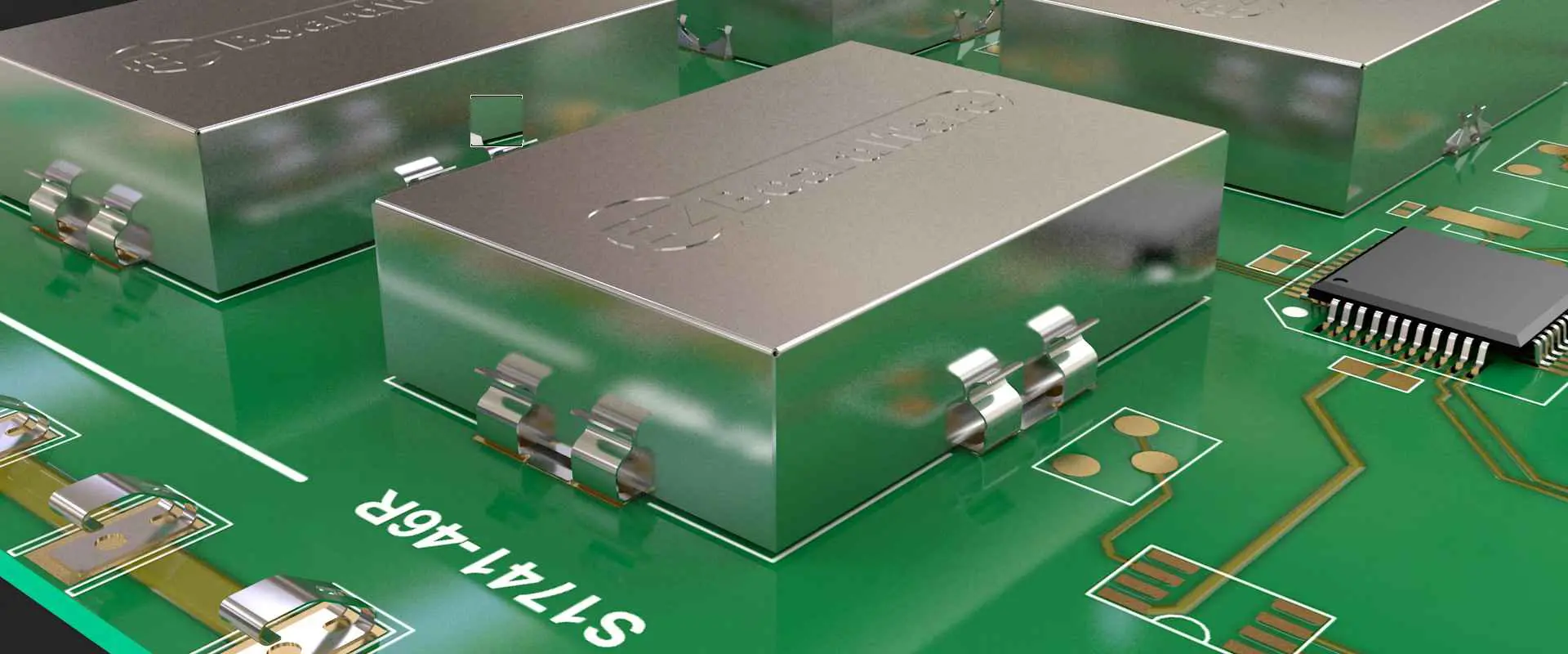
The Xilinx XC7A200T-2FBG676i is a high performance Field Programmable Gate Array (FPGA) part of the Artix-7 family built on a 28nm process. This article provides an overview of the XC7A200T architecture, key features, available development tools, and example applications leveraging this FPGA.

FPGA Overview

A field programmable gate array is an integrated circuit designed to be configured by the customer after manufacturing. FPGAs contain:

  • Configurable logic blocks to implement custom hardware logic functions
  • Programmable interconnects to route signals between logic blocks
  • Embedded memory blocks including block RAM and registers
  • Input/output ports and transceivers to interface with external peripherals

FPGAs provide the flexibility of software with the performance of custom ASIC hardware designs.

Xilinx Artix-7 FPGA Family

The Xilinx Artix-7 family delivers low cost, high performance FPGAs on a 28nm process optimized for cost sensitive applications:

  • High density variants with over 200K logic cells
  • Mixed signal options with up to 16 ADC channels
  • Low power versions optimized for power efficiency
  • Industrial temperature range support from -40C to +100C

The Artix-7 combines high performance with small form factors. The family targets applications like broadcast, medical, and embedded vision requiring low power along with DSP and real-time control.

XC7A200T FPGA Overview

The Xilinx XC7A200T specifically provides:

  • 218,600 logic cells in 11,661 logic slices
  • 655KB of fast block RAM
  • 240 DSP slices using 25×18 multipliers
  • Robust clock management with 8 PLLs and 16 clock management tiles
  • High speed transceivers up to 12.5Gb/s
  • Two 12-bit 1MSPS analog-to-digital converters

The large programmable logic capacity supports complex designs. DSP blocks allow high performance math-intensive processing. The XC7A200T provides flexible digital processing for a wide range of applications.

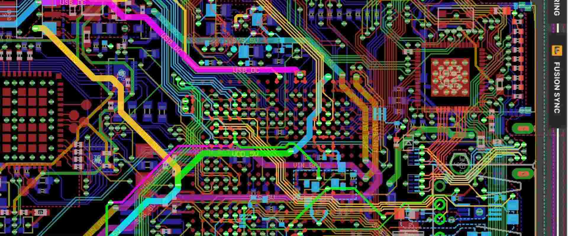
Internal Architecture

Inside the FPGA, the key programmable elements include:

Configurable Logic Blocks (CLBs)

  • Basic logic cell providing LUTs and flip-flops
  • Combinable into more complex logic functions

Block RAM (BRAM)

  • 36Kb memory blocks to implement data buffers and caches

Digital Signal Processing (DSP) Slices

  • Fast arithmetic units for high performance math

Input/Output Blocks (IOBs)

  • Support high speed differential I/O standards

Clock Management Tiles (CMTs)

  • Provide clock synthesis, conditioning, and distribution

Analog-to-Digital Converters (ADCs)

  • Integrated data converters to capture analog signals

Interconnects route signals between these blocks. The FPGA fabric can be programmed to create almost any digital system.

Development Tools

Xilinx provides a comprehensive suite of development tools:

Vivado Design Suite

  • All Programmable SoC architecture
  • Design entry using IP integrator and block design
  • Synthesis, place and route to generate programming files
  • Hardware debug with signal tap logic analyzer

SDx Development Environment

  • C/C++ and OpenCL programming with libraries for connectivity, math, video
  • Debug and profiling capabilties
  • Ability to integrate custom IP
  • High level synthesis for converting algorithms to RTL

Embedded Development Kit (EDK)

  • Tools for embedded processing hardware design
  • Standalone embedded processor creation
  • Integrated MicroBlaze soft-core CPU

System Generator for DSP

  • Xilinx blockset for high performance DSP design in Simulink
  • Bit accurate model simulation
  • Automatic generation of RTL from Simulink models

Xilinx provides the software and IP infrastructure needed for productive FPGA designs leveraging VHDL, Verilog or higher level programming.

Applications

Xilinx Chips
Xilinx Chips

The Artix-7 family excels in high bandwidth, power sensitive embedded applications including:

Embedded Vision – Low latency image processing for machine inspection

Industrial Automation – Real-time motor servo control

Alternative Energy – Smart grid management systems

Medical – Ultrasound and imaging systems

Broadcast – Video connectivity and encoding

Military/Aerospace – Rugged airborne controls and signal processing

Automotive – Advanced driver assist (ADAS) systems

FPGA flexibility allows tailoring to exact algorithmic needs versus fixed function ASICs.

XC7A200T-2FBG676i Specifics

Let’s examine key details of this particular Artix-7 variant:

Grade

  • 2 – Industrial temperature range (-40C to +100C)

Package

  • FBG676 – 27x27mm 1.0mm ball pitch flip-chip BGA with 676 balls

Speed

  • -2 – Up to -2 speed grade, supporting clock rates up to 550MHz

This combination provides a high density FPGA with robust thermal and mechanical characteristics required for industrial usage.

Summary

The Xilinx XC7A200T-2FBG676i provides a high logic capacity, low power Artix-7 FPGA suitable for embedded systems requiring significant real-time processing power. The partโ€™s large programmable fabric, abundant memory blocks, high speed I/O, and thermal resilience allow implementing complex algorithms and control logic for industrial electronics. Xilinxโ€™s comprehensive development tools enable design, debug, and programming targeting this 28nm FPGA.

XC7A200T-2FBG676i FPGA – FAQ

Q: What is the main benefit of using an FPGA like the XC7A200T vs a microcontroller or ASIC?

A: FPGAs provide custom hardware performance without the high upfront cost and lead time of an ASIC. This allows hardware acceleration of algorithms with more flexibility than hard silicon ASICs or off-the-shelf microcontrollers.

Q: What is the advantage of the flip-chip BGA package used on the XC7A200T-2FBG676i?

A: The flip-chip BGA provides a very dense, low inductance interconnect to the PCB allowing high bandwidth signal transfer over the large number of I/O balls. This facilitates maximizing performance in computationally intensive designs.

Q: What clock speed is supported by the XC7A200T after configuration?

A: The -2 speed grade Artix-7 supports clock rates up to 550MHz, enabling high speed register-to-register performance. Actual system speed depends on the user’s specific implementation.

Q: What is the typical power consumption of the XC7A200T FPGA?

A: Static power is 125mW. Active power ranges from 2.4W for 100MHz operation up to 5W for 550MHz peak operation. The low 28nm static power facilitates battery operated and green energy applications.

Q: What real-time control interfaces are supported by the XC7A200T FPGA?

A: The FPGA integrates hard cores for Ethernet, PCIe, CANbus, and GPIO providing standard real-time communication with external systems.

Looking for Xilinx XC7A200T-2FBG676i FPGA Quote

Field Programmable Gate Array (FPGA) used to be only used with electronics engineering. However, the use case or application is taking a new dimension with the integration of FPGAs in software development.

No doubt, there are several FPGAs in the market with each of them promising to offer better features than the others do.

That notwithstanding, there are a couple of Field Programmable Gate Arrays that can be used across different applications. One of such FPGAs is XC7A200T-2FBG676i.

In this article, you will learn more about this FPGA, as well as the applications and components.

What is XC7A200T-2FBG676i?

XC7A200T-2FBG676i is a Field Programmable Gaye Array (FPGA) that is categorized under Xilinx 7 Series FPGA family. Xilinx is one of the core manufacturers of Field Programmable Gate Arrays (FPGAs).

The XC7A200T-2FBG676i has programmable logic, which makes it easier for the designer, the software developer, or the consumer to re-program or remodels the FPGA for any other applications.

Technical Attributes

Like any other Field Programmable Gate Array (FPGA) out there, the XC7A200T-2FBG676i has a variety of technical specifications/features.

We have explained some of them below so you will understand what you should expect from the FPGA.

1. Macrocells

This Field Programmable Gate Array (FPGA) has digital logic components incorporated into the design. These logic components are also known as Logic Cells.

The XC7A200T-2FBG676i has Logic Cells of 215,360. Going by the functions of Logic Cells, this number is quite impressive.

Ideally, Logic Cells are the basic building blocks in a Configurable Logic Board (CLB). The Logic Cells often comprise a Configurable Register, as well as five product terms.

One of the main attributes of Logic Cells is that the cells can be configured. The configuration can either be done individually or by the sequential or combinational logic operation.

Logic Cells that perform this function are also called Macrocells.

As a designer, software provider, or consumer, you can be confident that the XC7A200T-2FBG676i will deliver the kind of precision you expect from a Field Programmable Gate Array (FPGA).

2. Voltage

Voltage is also one of the important factors to consider when looking for a Field Programmable gate Array (FPGA). It is important because you want to be sure that the FPGA can function optimally, without having to overheat.

In the case of the XC7A200T-2FBG676i, it has a voltage for different uses. The first is the 1.05V, which is the maximum voltage used for core supplies. The minimum core supply voltage is pegged at 950mv.

The Artix-7 Family Connection

XC7A200T-2FBG676i is one of the Field Programmable Gate Arrays (FPGAs) under the Xilinx Artix-7 Series.

As a member of this FPGA family, the Gate Array is used to tackle most of the challenges with software engineering.

Some of the issues tackled are:

1. Better Functionality

Currently, there is limited room for the integration of several components in a circuit board. Therefore, it is paramount that advanced functionality is created to bolster the integration of more components that would improve the efficiency of the circuit board.

2. Power Management

Excess power can trigger issues on a circuit board. Likewise, a limited power supply may reduce the efficiency of the board.

3. Cost Management

It is also imperative to improve the efficiency of circuit boards while reducing costs.

Those are some of the issues that the XC7A200T-2FBG676i solves to a greater extent.

The Solutions Offered by XC7A200T-2FBG676i FPGA

To tackle those issues above, here are the applications of the XC7A200T-2FBG676i. This Field Programmable Gate Array (FPGA) can solve most of the challenges with current circuit boards.

To do that, here is the wide range of features that would be leveraged to improve the efficiency and functionality of the gate array:

1. Faster Processor

One of the main advantages of the XC7A200T-2FBG676i Field Programmable Gate Array (FPGA) is that it has a fast processor โ€“ just like the other FPGAs under the Artix-7 Series.

The faster processor that comes with this gate array includes multiple features that would be used to improve the efficiency of the circuit.

First, there is the Application Processor Configuration that allows the designers or consumers to configure the gate array for different applications.

The second aspect of the fast processor is the over 200DMIPs of processing power. That way, the gate array can process faster and get the configuration or reconfiguration done in the shortest time possible.

The third aspect of the fast processor is the Real-Time Processor. This is impressive, considering that the gate array needs to process all that it needs to process in the shortest time possible. The work of the Real-Time Processor is to ensure that the gate array is faster when compared to other processors in other Field Programmable Gate Arrays (FPGAs).

Last but not least โ€“ the XC7A200T-2FBG676i Field Programmable Gate Array (FPGA) is powered by the MicroBlaze soft processor. This is the primary processor that coordinates most of the processing power and functionalities of the gate array.

2. Power Reduction

The XC7A200T-2FBG676i FPGA also does something to address the power challenges with traditional circuit boards.

This gate array deploys different power reduction mechanisms to ensure that the gate array works optimally.

The first power reduction metric used on the XC7A200T-2FBG676i FPGA is the 50% total power capacity. This means that the gate array can reduce up to 50% more power than the other FPGAs can.

3. Instant Development

Is it possible to develop or reprogram a Field Programmable Gate Array (FPGA) in a couple of hours?

This seems to be the logic behind FPGAs because they are meant to reduce the hassles associated with developing or building circuit boards with Application Specific Integrated Circuit (ASIC).

However, not all FPGAs can bolster instant circuit development – or at the shortest time possible.

However, the XC7A200T-2FBG676i Field Programmable Gate Array (FPGA) proves to do otherwise.

This FPGA assures designers and consumers of instant development and reconfiguration of circuits and associated components.

The instant circuit board development and or reconfiguration is because of the Linux support for the MicroBlaze processor. The MicroBlaze processor comes with a drag and drop functionality, which empowers designers and consumers to reconfigure or remodel the FPGA to their taste.

Conclusion

The XC7A200T-2FBG676i is one of the best Field Programmable Gate Arrays (FPGAs) you will find out there.

Just make sure you are experienced with FPGA reconfiguration or reprogramming so you can get the most out of it.

As an alternative, you may want to contact a professional FPGA engineer to do the job for you at the most affordable cost.

What is Autocad PCB ?

Autocad PCB

When it comes to designs, there are many tools designers can use. However, professional designers need to use simple and quality tools for their designs. The right tool you can use at the moment is AutoCAD for your PCB designs. You can expand your knowledge of design by using this computer software not only for designs but also for drawing.

YouTube video

The question some designers always have is: “How does the AutoCAD PCB work?” Or “Is the AutoCAD PCB reliable and easy to use?” Your questions are quite valid. In this article, as a beginner or pro in designs, you shall learn accurately how to use this software for your drawings and designs. At the end of your reading, you shall find it so interesting to use the AutoCAD PCB effortlessly for designs. We shall also raise some frequently asked questions, providing affirmative answers to them.

What is an AutoCAD?

It is paramount to understand what an AutoCAD does. This will help anyone who wants vast knowledge about designs know more. It is computer software that anyone can use for designs professionally. This is known as a system or computer-aided design (CAD) that is primarily used for making designs and drawings faster and more accurate.

AutoCAD is not only used by designers. Others who use it are project managers, regional planners, engineers, architects, constructors, and several other experts in the world of design. If you know how to use this software for designs properly, there is no advanced design software you probably would not learn how to use. The Autodesk Company is in charge of this software, AutoCAD. With this software, PCB designs are done faster.

One interesting fact about using this software for designs is the ability to draw faster than using your hands. Some designers still make use of their hands to draw. This is a digital world where everything has become easier with the aid of software applications. The 2D design is made possible using this software. Not only can you draw with it. It is easier to edit your 3D designs using AutoCAD. You can draw any digital designs using this software application. Designing, drawing, as well as editing, can be done faster with AutoCAD.

As a learner whose interest is becoming a professional in your industry, it is very crucial to advance your skill in the world of design. With this computer-aided design software, you can make more commercial gains. This is because your drawings and designs come out flawlessly. Above all, with this software, you can use any design software in the nearย future.

Why Do I Need To Advance My PCB Design Using AutoCAD?

autodesk pcb

It is very important to advance your drawings and designs. This is because the industry has become highly competitive. Everyone wants to be recognized for what they do. Design is fast becoming trendy across the globe. Most professional designers and content developers use AutoCAD.

With this software, there is hardly any design you cannot come up with. Architectural designs and drawings are done with AutoCAD. Building projects involving designs are also perfectly done with this software. You too can achieve artistic, digital drawings using AutoCAD. Developing one’s creative designing skills can be greatly achieved with the right tool.

Let us thoroughly consider the reasons you should use AutoCAD. These are cogent points that help you develop your PCB design skills.

Makes You Become a Professional

With the aid of the AutoCAD for PCB design, you too can become a pro at design. This is why you need advancement in your PCB drawings. If you are into interior design, you need to get this software. Rather than creating designs with the hand, use this tool. If you indeed want to hone your design and editing skill, you need to use the AutoCAD tool very well. AutoCAD makes the world of design easier. Any professional would opt for this software.

You Can Create 3D Printing

Interestingly, the world is becoming advanced. You do not want to get caught unaware. In the digital space, creating a 3D print is possible. With the CAD model, you can print objects perfectly. Additive manufacturing becomes stress-free using the software.

You can create any three-dimensional object you want as long as you have this tool. With this CAD model, objects with any color, shape, or size can become trendy.

Teaching Others

Yes, this is another reason to advance your PCB design skills. When you are good at designing, it becomes an avenue to teach others. There are master classes organize for design, drawing, and digital classes.

Autodesk ensures that using AutoCAD gets easier every day. This is why children can also learn how to design using AutoCAD. Teaching your kids how to draw won’t be a bad idea, either.

Make More Money

Definitely, everyone wants to make more money. If you advance your PCB drawing and design, there are chances that you make more money than your competitors. AutoCAD is rightly available for use on mobile devices. This means that you can have this designing tool on your tablet or phone.

Reduces Error:

This is one of the reasons professionals use this software application. One way to advance your PCB design is using AutoCAD. It decreases possible errors while designing.

Fast For Sharing Collaboration

There is the assurance that with the AutoCAD, you can easily and quickly share collaboration. It is compatible with any kind of software. It can work with every other software application.

Saves Time

Isn’t so interesting that you can save time? With the AutoCAD PCB, you can be productive while saving time. You do not have to spend long days on designs and drawings. This is because this application handles your drawings in a very fast way. It saves you stress.

Fun Facts About Using AutoCAD For PCB design

It is noteworthy that AutoCAD is available in more than 12 languages. This implies that many people across the globe can use it. It has no restrictions on its use. Language is never a barrier to advancing your PCB design skills. The AutoCAD is available in German, French, Czech, Spanish, and English among other languages. Designing becomes more interesting when you can learn in your own language.

Another interesting fact with AutoCAD is that it can easily adapt to varying drawing and design requirements. You can easily use it for any drawing project of your choice. It can prototype any vital product parts. Interestingly, this software tool can forecast the outcome of your project. It aids easy access to visualization. It allows for section planes. The planes automatically help create some views of your 3D models.

What Are The Features of AutoCAD?

The Autodesk company that develops this software ensures that it comes with some amazing features.

Interface Customization: This feature makes it so possible for model editing to become much easier. There is no better way to model editing than using AutoCAD because of this feature. It also makes it super plausible to arrange the software tools for accessibility.

Installation: This is one of the best features of this software application. It is so easy to install. The installation as well as customization is very easy. It is not one of the tools that have difficulty with installation.

Multifunctional Grips: This is one advantage of using this software application for your designs. It comes with multiple grips for easier design.

Visual Styles: There is no better design application that gives room for varying visual styles. The AutoCAD helps with a lot of visual styles.

Photo Studio: Among its numerous features, this tool allows for a photo studio. It makes it plausible to display your design and pictures.

3D Capacity: This is a feature distinct from this software. It has the capability to visualize 3D designs and printings.

Other featuresย of this software include; 3D navigation, Mesh modeling, text settings, express tools, sheet set manager, 2D drafting, online maps, among other features.

More on PCB Design

Autodesk PCB allows designs to come out in creative versions. PCB design begins with a process and this is through the conversion of any schematic image to the PCB layout. Autodesk eagle free is for PCB design. It is an electronic design for every circuit drawing.

AutoCAD PCB design is what any designer wants to achieve. It is simple as long as you have the software application. Printed circuit board design with the aid of AutoCAD gives the professional design anyone desires.

Autodesk eagle price for design is not less than $510.00 each year. That is for the Eagle Premium, although there is also the free version of Eagle. The AutoCAD helps with PCB drawing and design. The PCB design comes based on the kind of holes as well as the volume of layers.

Conclusion

It is very paramount to use the right tool for design. It makes the work quite easier. Reading through this article, one begins to note that AutoCAD helps with proper PCB design. As a designer in the fashion industry, you can use this software application for your creative design.

It is not only exclusive to some fields. Anyone, be it a beginner or pro, can use the AutoCAD PCB. Reasons you need to use this software have been stated above. Kindly learn to use it to become better at designing.

Top 15 Electronic Design and Manufacturing (EDM) Companies

electronic design and manufacturing

Original design manufacturing (ODM) and electronic manufacturing services (EMS) providers deliver comprehensive solutions spanning concept to high volume production for electronic products. This article profiles the top 15 electronic design and manufacturing (EDM) companies worldwide recognized for capabilities across hardware, software, manufacturing technology, and global supply chain operations.

1. Flex

Singapore-based Flex describes itself as the โ€œsketch-to-scaleโ€ solutions company. Capabilities include:

  • Multi-disciplinary engineering across electrical, mechanical, software
  • Comprehensive SMT, machining, plastics manufacturing technologies
  • Next-gen connected IoT products and edge solutions
  • Supply chain network with over 100 sites worldwide
  • Industry 4.0 factory automation and optimization

Flex provides innovative product design through high volume, cost optimized manufacturing for diverse industries from automotive to energy to healthcare.

2. Jabil

Jabil is a leading global EMS provider headquartered in Florida with over 180 manufacturing sites across 30 plus countries. They deliver:

  • Product design, simulation, prototyping services
  • PCB fabrication, PCB, box build assembly
  • Complete product packaging and supply chain management
  • Comprehensive quality management
  • Aftermarket services like warranty repair
  • Focus on MW and RF manufacturing services

Jabil offers deep expertise in regulated industries like healthcare and automotive as well as end-to-end solutions from NPI to distribution.

3. Rayming Technology

Rayming Technology is ranked the top electronics manufacturing services provider based on its comprehensive solutions integrating industrial design, engineering, intelligent manufacturing systems, and global fulfillment. Key capabilities include:

Product Design – Industrial, mechanical, PCB, firmware/embedded software design services

Manufacturing Technologies – SMT production, machining, sheet metal fabrication, injection molding

Smart Factory Solutions – Machine connectivity, analytics, edge control systems

Manufacturing AI – Predictive quality, adaptive scheduling, automated inspection

Global Delivery – Manufacturing sites in Asia, Europe, and North America

Rayming enables customers to bring innovative connected products to market quickly through its expertise spanning electronic, mechanical, and software engineering combined with smart digital manufacturing capabilities.

4. Pegatron

Pegatron is a Taiwan based ODM with over 20 production facilities providing:

  • Product design, development and tooling
  • High quality, low cost manufacturing
  • Customization abilities for multiple product families
  • Supply chain optimization with component management
  • Manufacturing expertise across computing, networking, consumer electronics

Pegatron enables rapid optimization from design concepts to high volume manufacturing for major computing and communication brands.

5. Sanmina

Sanmina Corporation is a leading tier one EMS provider designing, manufacturing, distributing, and repairing electronic components across industries including:

  • Communications networks
  • Cloud solutions
  • Defense and aerospace
  • Industrial and semiconductor capital equipment
  • Multimedia and computing

Sanmina capabilities span engineering using tools like computational fluid dynamics, integrated supply chain management, and differentiated manufacturing technologies such as cables, backplanes, enclosures, specialized metal fabrication, and vertically integrated PCB fabrication.

6. Wistron

Wistron is a Taiwan based ODM providing design, manufacturing and after-sales services for major laptop and server brands. Key capabilities:

  • Product development including industrial, mechanical, software design
  • Higher level assembly including system integration and box build
  • Manufacturing expertise across computing, networking, and wireless communications
  • Global manufacturing and service presence including Americas, Europe, Asia
  • Rapid prototyping and new product introduction from concept to high volume

Wistron enables customers to focus on sales and marketing while leaving manufacturing design and execution to internal cross functional teams.

7. Compal Electronics

Compal is a leading Taiwan ODM providing joint design manufacturing (JDM) services. Capabilities include:

  • Notebook, All-in-One PC, server product design services
  • Extensive consumer electronics manufacturing expertise
  • Supply chain optimization with strategic component partners
  • Global manufacturing footprint with sites in China, Mexico, Vietnam
  • Quality and speed focused manufacturing culture

Compal collaborates closely with customers through JDM partnership benefits to deliver high quality, cost optimized products.

8. Creation Technologies

Creation Technologies is one of the largest electronic manufacturing services providers in North America. Services include:

  • Product design services
  • Rapid prototyping and new product introduction
  • SMT, through hole, box build assembly
  • System integration, multidisciplinary technology expertise
  • ISO certified manufacturing at multiple North America sites
  • ITAR registered and NADCAP accredited electronics assembly
  • Complete supply chain and logistics solutions

Creation Technologies enables customers with innovative products to launch rapidly into high volume North American and global production.

9. Key Tronic

Key Tronic is a leading EMS provider focused on engineering services, supply chain management and manufacturing. Capabilities include:

  • Concurrent engineering collaboration for design optimization
  • Integrated supply chain program management
  • SMT, thru-hole and automated assembly with precision automation
  • System integration, box build, racks, cables
  • Globally certified quality management system
  • Value added services like programming, laser etching, coatings

Key Tronic provides seamless transition from initial concept reviews to full-scale production ramps.

10. Benchmark Electronics

Benchmark Electronics is a leading EMS provider offering engineering, manufacturing, distribution, and advanced technology solutions. Capabilities span:

  • Product design including concept prototyping
  • SMT, thru-hole and conformal coating assembly
  • Volume box build manufacturing
  • Global material procurement and supply chain management
  • Advanced engineering capabilities like thermal analysis and microwave/RF
  • Precision machining, plating, coating metal fabrication
  • Sustainability initiatives like green manufacturing

Benchmark enables faster time-to-market and competitive differentiation. Their engineering-centric model provides close design collaboration.

11. Plexus

Plexus delivers optimized product realization solutions across 5 key market sectors:

  • Networking/communications
  • Healthcare/life sciences
  • Defense/security/aerospace
  • Industrial/commercial
  • Computing

Plexus capabilities include product conceptualization, design, commercialization, manufacturing, fulfillment, and sustaining services. Plexus Engineering, Manufacturing, and Aftermarket Services span the full product lifecycle.

12. Celestica

Celestica is a large multinational EMS company serving aerospace, industrial, healthtech, enterprise and telecom customers. Capabilities:

  • Joint Design Manufacturing partnerships
  • High mix, low to mid volume expertise
  • SMT, thru hole assembly, box build
  • System integration including racks, cables
  • Aftermarket repair, refurbishment, remanufacturing
  • Global network with major sites in NA, Europe, Asia

Celestica provides competitive ramps from prototype through high volume production across diverse end markets.

13. USI Electronics

USI is a specialized EMS provider focused on delivering miniaturized electronics manufacturing solutions with expertise in RF/microwave, microelectronics, and optoelectronics. Key capabilities include:

  • Microelectronic packaging and assembly
  • Component level inspection including x-ray and acoustic micro-imaging
  • Advanced optical packaging
  • High frequency and microwave PCB assembly
  • High mix low to medium volume focus
  • ITAR registered and ISO certified

USI services demanding end markets including aerospace, defense, telecom, medical, and industrial controls requiring precision microelectronic manufacturing.

14. SVI Electronics

SVI Electronics offers value-add engineering manufacturing services focused on industrial, instrumentation, and hi-rel market segments. Capabilities include:

  • High mix, low to medium volume expertise
  • Rapid prototyping through production
  • SMT and through-hole assembly
  • Box build and rack integration
  • Cable harnesses and electro-mechanical assemblies
  • Supply chain partnerships to ensure BOM availability

SVI serves startups or established OEMs needing responsive, flexible manufacturing services tailored to industrial electronics.

15. Spectrum Assembly

Spectrum Assembly provides contract manufacturing focused on low volume, high mix products. Capabilities include:

  • Prototype support through pilot manufacturing
  • SMT and thru hole assembly down to 0201 components
  • Design and layout services
  • Conformal coating, potting and encapsulation
  • Box build integration and functional testing
  • Supply chain management and procurement

Spectrum Assembly serves aerospace, defense, industrial, medical, and hi-rel customers needing low volume and rapid turn services.

Evaluation Criteria

The companies were evaluated on these key criteria to determine the top electronic design and manufacturing providers:

  • Breadth of end-to-end engineering design services offered
  • Advanced manufacturing technologies supported
  • Electronics industry experience and technical expertise
  • Manufacturing scale and global production footprint
  • Supply chain maturity and BOM management
  • Quality management and compliance certifications
  • New product introduction and prototyping agility
  • Focus on smart manufacturing, automation and data utilization
  • Reliability and customer satisfaction

Conclusion

Selecting the right EDM partner requires assessing capabilities across the product lifecycle from development through sustainment. The best providers collaborate as an extension of the product team while bringing design innovation, manufacturing excellence, and supply chain expertise. Leveraging an experienced EDM partner enables OEMs to deliver robust, differentiated products faster and more cost effectively.

Top Electronic Manufacturing Companies – FAQ

Q: What are the main differences between EMS and ODM providers?

A: ODMs provide deeper design services while EMS focus more on manufacturing. But top partners offer comprehensive services spanning concept design through volume production.

Q: What manufacturing capabilities should be expected from a top tier EDM partner?

A: SMT, thru hole, machining, injection molding, stamping, system integration, test development, automation, model shop rapid prototyping, and more.

Q: How do EDM companies help manage obsolescence and part shortages?

A: They leverage approved vendor lists, alternate part recommendation expertise, and inventory buffer stock strategies to prevent production line stops.

Q: What core competencies should an EDM partner have beyond manufacturing?

A: Strong program management, supply chain mastery, new product introduction processes, quality culture, data utilization, and continuous improvement focus.

Q: Why partner with an external EDM instead of building internal captive capabilities?

A: Faster launch speed, leverage manufacturing scale and expertise, labor cost arbitrage, focus internal resources on core differentiators.

Important things to consider before designing a PCB

  1. Your PCB producer necessities. Ensure you read the rules about file naming, power isolation, trances size, and pacing before you begin planning.

Data you should give to the PCB producer:

  • Gerber file
  • Copper Weight (0.5 oz (18 um), 2 oz (70 um),1 oz (35 um))
  • Surface Finish OSP (Organic Solderability Preservatives), DIG (Direct Immersion Gold), (ENIG (Electroless Nickel/Immersion Gold)
  • Color (Green, Black, Red)
  • Thickness
  • Material (FR-4 (woven glass and epoxy), FR-3 (cotton paper and epoxy), FR-2 (phenolic cotton paper))
  • Number of Layers
  •  PCB layers: The more layers, the more unpredictable the assembling of the PCB will be.  
  • Two layers normally for straight forward toy items
  • Four layers, usually for IoT related items
  • 6 to 8 layers typically for Smartwatch and phone.
  • PCB size โ€” this relies upon your item size (or walled-in area size). Item size is characterized during electronic product design and development.

PCB design process

electronic product design and development

Circuit design

The first step to designing a circuit is to come up with a schematic. It is a record, like an outline, that portrays how segments identify with one another and cooperate. To make a schematic record, you will require a product device. We like Quadcept, as it is upgraded for planning PCBs for assembling (for instance, you can trade your Bill of Materials (BoM) straight forwardly from the device) and, being cloud-based, it tends to be advantageously utilized anyplace.

After choosing the apparatus introduced, you need to get part determinations for every one of your chose segments. They are typically accessible on your merchants’ sites. The model records will assist you in drawing the schematic. When you transfer the model to the product apparatus, the part will be accessible in the data set. Then, you should follow the information sheet to connect the lines to each stick out of the parts.  

Every schematic image needs to have a related PCB impression that characterizes the fundamental elements of the segments and arrangement of the copper padding or through-hole on the PCB.

A decent schematic is genuinely significant. It will fill in as a kind of perspective record when you debug. It is an extraordinary, specialized device with a different electronic product designer. Likewise, electronic prototype companies can test the gadget by test focuses on this record.

PCB design and Gerber file

When creating a Gerber file and designing a PCB layout, one can use tools such as DipTrace, ORCAD, PADs, Cadence Allegro, KiCad, Upverter, ExpressPCB, and Altium. In contrast to the schematic, the PCB format dispenses the real segments to the specific area on the PCB and shows the follow to join every part together between the PCB layers. The higher the number of layers you have, the more unpredictable assembling it will need, and it will be even more expensive.

Separate the PCB into legitimate areas as indicated by the usefulness. Then, at that point, try to bunch the segments of each segment in a similar region.

UI is additionally something you need to remember when during electronic design manufacturing. Areas of the segments like sound jacks, connectors, LEDs, and so forth should be adapted to the best client experience conceivable.

At the point when you finish the format plan, you produce a Gerber record. Your PCBA producer will utilize this record.

Positioning of components on the PCB is vital. A few parts may meddle with one another and cause surprising practices. For instance, if you have Wi-Fi and Bluetooth modules, they have a similar 2.4 GHz transmission capacity and can meddle with one another if not set effectively.

PCB manufacturing

Any PCB manufacturer can design and print out an exemplary circuit board according to your specification if you give them your Gerber file. It is the fundamental step to starting and advancing in adding additional components.

Material preparation

Now in your EE plan, you should choose segments. You can either request that your PCBA producer request the necessary parts for you or do it without anyone’s help if you have sellers chosen. Things to remember:

  • Losses: Order ten percent more to cover up for any loses
  • Minimum Order Quantity: If you are not purchasing exactly the base, ensure the chosen parts are available. For small amounts, you can arrange online from DigiKey or Mouser. For more substantial amounts, ask your producer for proposals.
  • Packaging: request parts in reels for SMT machine auto-pick up, not in isolated bundles
  • Lead time: as these parts come from various sellers, remember the lead time. It very well may be up to 8 four months for certain segments.

Mounting the Components on the PCB

There are two principle techniques for putting parts on the PCB surface:

  • SMT (Surface Mount Technology) strategy is the most generally utilized in mass assembling. It is finished by quick and exact SMT machines that save you time, cash, and stay away from a human mistake.
  • Through-hole: A manual strategy for fitting segments with wire leads to openings on the PCB surface. It is additionally regularly called Dual In-line Package or DIP process.

Things to keep in mind:

  • Any segments that you should add physically with through opening strategy will add to the assembling cost.
    • Some greater parts cannot be mounted by the machine and still need manual through opening work. In this manner, both advances can be utilized on a similar board.
    • Check what impression cushion measures your producer upholds. In any case, the SMT machine will not mount the parts effectively.
    • Optimize and solidify your segments to have only one SMT run.
    • Your part type number ought not to surpass the quantity of reels the SMT machines of your maker can uphold.

Reflow

We refer to the procedure of making the segments “stick” to the PCB as reflow soldering. The PCBA goes through a reflow heater or an infrared light that warms up the board until the weld liquefies, for all time interfacing the board and the different components.

The exciting part here is not damaging the components or overheating since each bundle has different heat profiles. A dependable PCBA producer will deal with this interaction, and all you need is to give the segment determinations to them.

Other soldering techniques:

  • Iron soldering can be utilized in explicit cases, however not ordinarily in mass assembling.
  • Wave soldering is generally utilized for the segments added physically, utilizing the through opening technique. In these cases, your PCBA will initially go through a reflow stove, and afterward, in the wake of adding different parts physically, it will go through a wave fastening machine.

Testing and QA

In this progression, an example of PCBAs will be tried to guarantee quality. Basic missteps are disjointed components, skewed parts, and shorts that interface segments of the circuit that should not be associated. Most basic tests:

  1. X-beam: The PCBA producers will utilize X-beam to check the soldering conditions for BGA (Ball Grid Array) segments.
  2. AOI (Automatic Optical Inspection). The makers use “brilliant example” โ€” a reference PCBA to contrast and others. For this test, the equipment makers should give the particulars and resistance to the producer to set the boundaries.
  3. ICT (In-circuit Test): When you plan the PCB, you regularly will save some test focuses for troubleshooting, programming, and different purposes. The ICT machine will utilize these tests focuses on doing the open/short test. It will check if the upsides of the latent parts (capacitors, inductors, resistors) are in inside determinations.

Electronic design and manufacturing Trends You Should Know in 2023

Here is a gander at the moving strategies that top PCB makers utilize to improve their electronic system design and manufacturing and improve execution.

The IoT is spreading all over, and we have come to understand that each gadget should be shrewd in the computerized time. A similar direction is occurring with PCBs. It then pushes an electronic product designer to make orchestrated and adjusted forms of their plans. Nowadays, we see multi-facet and an assortment of low-volume PCBs.

PCBA is getting difficult for individuals who do not utilize the most recent PCB-producing patterns. At first, you may require a low-volume PCB get-together to test the PCB-based item before moving onto large-scale manufacturing.

As the PCB business grows to satisfy IoT needs, it is likewise encountering increasing expenses. Thus, more makers are going to the most recent PCB configuration patterns.

High-Power Boards in High Demand

Innovation now permits makers to assemble high-power PCBs that can oversee voltage over 48 V. It opens a way for high-power board establishment into a more extensive territory for gadgets.

The justification for expanding the power of PCBs is that they can work with multiple components. With an upgraded battery bundle, the PCB can work longer. In addition, PCBs are turning out to be more slender and more lightweight, improving their productivity, heat retention capacity, and solidness.

PCB Autoplacers

Today, PCB producers remember autoplacers for their electronic design manufacturing. As a result, this computerization cycle has gotten substantially more proficient and helps smooth electronic-gadget activity.

Computerization measures for building autorouters are big life hacks. Thus, these autoplacer measures are helping improved operational quality and speed time-to-advertise.

Notwithstanding the more noteworthy speed, producers are hoping to coordinate CAD frameworks into the interaction. Because of autoplacers and adaptable plan programming, PCB fabricating, particularly multi-facet PCBs, is a lot smoother and simpler.

Biodegradable PCBs

Electronic waste administration issues have become a worldwide concern. To help balance those issues, biodegradable PCBs are ascending in notoriety.

The disposal of PCBs, commonly the biggest segment of electronic gadgets, was destructive to the climate because of the synthetic substances utilized in them. The biodegradable forms dispense with those issues. Moreover, some businesses support extricating metals from E-squander, including palladium, silver, gold, gallium, and tantalum, which they can reuse through refining.

Adaptable PCBs

A PCB’s adaptability is vital because it permits a solitary board to deal with a few capacities. Low-volume PCB gathering requires the adaptability to put a few parts on a solitary board.

It should not shock anyone that adaptable PCBs are now getting better than their unbending PCB partners because of the capacity to deal with mode stress and bowing properties. However, it is not sure whether it will convert into deals development. However, adaptable PCBs are regardless mainstream among clients.

Conclusion

The life of a PCB goes from plan to model. Then, the development of low-volume PCBA, lastly, large-scale manufacturing. Innovation keeps on clearing a smoother way on the assembling front, so expect many more PCB innovation changes to arise in the impending years.

An Introduction About IC Reball

ic reball

IC Reball is a kind of rework technique, which is used to repair faulty circuit board components such as ICs, resistors, capacitors etc. It also can be used to diagnose and repair PCBs.

YouTube video

Reballing is mainly used for BGA and PGA chips with BGA balls cracked or missing that are unrepairable by other means. It can be used to repair ICs, resistors, capacitors on circuit boards with damaged or missing solder pads that are not repairable by other means.

The IC Reballing process is a very time consuming, labor intensive process. If you have a circuit board that has been damaged to the point where the components are no longer repairable, then Reballing may be an option to consider in order to save the PCB from being scrapped.

There are many steps involved in Reballing and it’s a process that takes time and knowledge to complete successfully.

IC Reballing is a process that uses solder paste and a dedicated stencil printer to place solder paste onto all of the pads on the circuit board. The ICs, resistors, capacitors or diodes are then removed from the old PCB and placed on top of the new solder paste using tweezers or forceps. The new component is placed on the solder paste covered pad and pressed down firmly onto it. This is repeated until all of the pads have been replaced with new components. Power is applied to the circuit board and then the resistors, capacitors and diodes are tested. If everything checks out then the board is returned to the user for use.

Rebalancing is a process that is used to repair BGA balls that have cracked or been missing for some time. BGA balls are typically used on motherboards and in place of solder pads on IC sockets. They are designed to be hot-soldered into place but over time they may become loosened or damaged. This can result in instability and intermittent operation of the socket so it needs to be repaired as soon as possible.

How to Reball a circuit board:

The first step in reballing is to remove the defective component from the circuit board. This can be done using a soldering iron, tweezers or forceps. The old solder is then removed using a desoldering braid or wick. A new BGA reballing station is used to place the new BGA component on the circuit board using a solder paste stencil and laser head. The new BGA component is then soldered onto the circuit board. The new component is tested and then the circuit board is returned to the customer.

What is the process of reballing BGA chip?

BGA chips have solder balls on the underside of the chip which transfer power and data to the PCB. The ICs, resistors, capacitors and diodes need to be replaced with new components with new solder balls since the old solder balls have cracked or been missing for some time.

The process of reballing BGA chip is as follows:

1) First remove all of the old ICs, resistors, capacitors and diodes from the PCB.

2) Clean the PCB with Acetone or Isopropyl Alcohol and allow it to dry.

3) Reball the ICs, resistors, capacitors and diodes by placing them on a BGA Reballing Station. Press down firmly onto the solder balls with your fingers and apply power. The ICs, resistors, capacitors or diodes should be tested for operation and then returned to the PCB.

4) Using tweezers or forceps, place the new BGA ICs, resistors, capacitors or diodes onto the solder balls. The BGA chips are placed directly onto the solder balls or on top of a new substrate. Once in place they should be pressed down firmly and then power applied again.

5) Wipe away any excess solder paste with a sponge using Acetone or Isopropyl Alcohol. Remove any excess liquid with a cloth and allow to dry.

6) Using a magnifying glass, check the solder balls for solder bridges. If you find any then they should be removed with a solder wick.

7) The final step is to use a multimeter to test all of the new components and make sure that they are functioning properly.

What is a BGA Reballing Station:

bga reballing station

A BGA Reballing Station is used to Reball ICs, resistors and capacitors. It is a dedicated station that will allow you to replace the damaged BGA components on circuit boards with the same type of components.

A standard BGA reball station is made up of an X-Axis,Y-Axis,Z-Axis and a laser head that can be rotated 360 degrees for reballing of different types of boards. It will have a heated PCB bed which allows for better soldering quality and a stencil printer that will allow you to print the reballing stencils.

Reballing PCBs can be very time consuming and labor intensive, especially when you have multiple boards to restencil in one day. A BGA Reballing Station will allow you to quickly and accurately reball your circuit boards.

What is an IC Reballing Stencil?

A Reballing Stencil is a piece of paper that has a pattern printed on it and contains all of the information that you need to Reball your circuit board.

The stencil is printed on paper with a conductive ink so that it can be used to apply solder paste to the circuit board when you are reballing. The stencil also contains the pattern for the ICs, resistors and capacitors that you will be replacing.

IC Reballing Stencils are available with different types of patterns.

Must you use an IC Reballing Stencil?

If you have never worked with Reballing before, it is suggested that you use a stencil to start. Not only will the stencil make your first Reballing project easier to complete, but it will also ensure that all of your solder paste is applied evenly to the pads on the PCB. You may get away without using a stencil for your first few Reballing projects, but it is highly recommended that you use one as you gain more experience in the process.

However, after you get good at reballing, you may not need to use one. It depends on the BGA chips or process of reballing PCBs that are used. If you like to learn how reballing ic without stencil is done, weโ€™re covering it in the next section.

There are methods to effectively Reballing ic without stencil.

There are some reballing techniques that don’t use a stencil or a PCB with solder paste already on it. Instead, you may have to use a paste dispenser to apply the solder paste to each of the areas where you will be replacing components. This is not an easy thing to do and takes a lot of practice so that you can become proficient in this process.

The best Reballing without stencil method is as follows.

When you don’t use a stencil, you have to do more steps.

Step 1: Clean the old solder paste from ball pads.

Firstly, you will need to clean the old solder paste from the ball pads. You might need to use some chemicals to remove old solder paste.

Step 2: Apply new solder paste on ball pads.

After all old solder paste is removed, you need to apply new solder paste on the ball pads. Use a paste dispenser for this step.

Step 3: Remove ICs, resistors and capacitors from the old PCB board.

You can remove ICs, resistors and capacitors from the old PCB board by using tweezers.

Step 4: Place ICs, resistors and capacitors on the new solder paste.

After all ICs, resistors and capacitors are removed from the old PCB boards, you can place them on the new solder paste.

Step 5: Place ICs, resistors and capacitors on ball pads.

After all components are placed on the new solder paste, you can place them on the ball pads.

Step 6: Remove ICs, resistors and capacitors from the new solder paste.

Then you will need to remove ICs, resistors and capacitors from the new solder paste. Use tweezers for this step.

Step 7: Reball the PCB board.

After all ICs, resistors and capacitors are removed from the new solder paste, you can reball the PCB board. Power is applied to the PCB board and then all components are tested. If all components work, you can return the PCB board to the users.

Almost every circuit board repair service today has IC Reballing as part of their services. The ability to repair a circuit board that would otherwise be scrapped because it is beyond repair by other means is what makes IC Reballing such an important service for PCB assembly companies and end users alike.

IC Reballing is a very time consuming process that requires a lot of patience and practice to master. It is not a process that can be learned in a few days or a week. It takes time to learn and master this process and it is a skill that requires constant practice to keep sharp.

What is PCB Shield ?

PCB Shield

PCB Shielding is the mechanical method of using conductive, magnetic or both materials to prevent EMI in the system. Mechanical shields are closed, conductive containers, connected to the ground of the PCB. They effectively decrease loop antenna sizes, and absorb and/or reflect some of the radiation.

Undesired Electromagnetic Emissions in Printed Circuit Boards

Any product with contains wires or traces and operating at high-frequency emits radio waves. As Printed Circuited Boards – PCBs become smaller and faster, one drawback of this emergent technology is severe Electromagnetic Compatibility (EMC) problems. Electronic systems consists of printed circuit boards (PCBs), interconnect, integrated chips, and I/O cables. Based on the current carried by the conductors, and the length of interconnects, these interconnects imitate antennas when working at high frequencies, sending out EMI.

YouTube video

Electromagnetic Compatibility – EMC

EMC determines if a device is compatible with its electromagnetic environment, and does not cause interference. If it does not emit levels of EM energy that causes electromagnetic interference (EMI) in other devices in the vicinity, it is said to be Electromagnetically Compatible. There are international standards that specify the level of emissions. Thus, manufacturers must monitor and measure electromagnetic radiation to control them. Lack of compatibility can cause narrow and broad band interference to other electronic equipment in close range, as well as data leakage.

Effects of EMI

EMI shield PCB

Energy causing EMI can be in the form of conducted, radiated, and electrostatic discharge (ESD). EMI may even physically damage operational equipment, hence undesired electromagnetic (EM) emissions represent one of the most critical issues to be accounted for in electronic system design. EMC makes sure that systems perform as intended under the defined safety measures. The EMC process monitors testing requirements, and interference between the equipment placed in close proximity to each other on the PCB. Although it can occur in any frequency range, it usually occurs above 50MHz, in such cases, grounding, EMI shielding and focusing on trace spacing and layout during design phase.

Designing PCBs with EMC

There are certain simple PCB design guidelines for electromagnetic compatibility that save time and costs.

  • All high-speed signals on a PCB should be referenced to a solid plane. A model return path for such signals on the circuit board is a large area of metal (ground copper polygon placed in adjacent layers to the differential pair signal), or a plane layer. This becomes the reference plane.
  • Current flow in any trace on a PCB must complete the entire circuit loop and come back to the source through the reference plane. Current in a performing PCB flows from the power supply or from outputs to further downstream components.
  • Return current should always choose the path of least โ€œimpedanceโ€ and will form the smallest loop with respect to the incident current path to minimize loop inductance.

One way of handling unwanted EMI is through PCB shielding.

Arduino Circuit Boards

Arduino circuit boards are produced as ready to use, and contain all required operational circuitry. Its core contains a compacted Atmega328 chip microcontroller/computer. The Arduino platform contains LEDs, connections, microcontrollers, and more. Arduino circuit boards power themselves through current supply through USB port using a USB cable. AC-to-DC power adapters can be used for external power supply.

Types of Arduino Circuit Boards

Arduino circuit boards are open source. This makes it easy for users to tailor-make projects and instruments. There are several Arduino boards available including:

  • Arduino UNO,
  • Red Board,
  • LilyPad Arduino,
  • Arduino Leonardo,
  • Arduino Mega.

Each of the above are different in specifications, features and uses, and how they are used in different electronics projects. For the purpose of this article, we will focus on the Arduino Mega boards and Arduino Mega Protoshield.

Reflection and Absorption

EMI/EMC shielding can be used to encase a part of the system or the whole system. This protects the signal transmission from external noise and prevents information loss. Shielding has two chief purposes:

  • Reflection (R) occurs when energy from an electromagnetic wave runs into the shield and is reflected back. and
  • Absorption (A) takes place when any residual energy from the electromagnetic wave that is not reflected is absorbed in the shield, and the residual energy exits from the other side.

How to Shield a PCB

Metal shields or cans are added to shield a circuit board from EMI, in order to contain critical areas on the PCB. Shielding covering four sides and the top is soldered down to the ground plane under the components. This type of shielding is called a Faraday cage. Ideally the shield should completely enclose components to block off all emissions. However, shield openings are required for thermal cooling, seams, adjustments, and solder points to the board.

Types of PCB Shielding

PCB RF Shielding

Electromagnetic Interference shielding or EMI shielding that impedes radio frequencies and electromagnetic radiation is called RF shielding. This type of shielding reduces the coupling of radio waves, electromagnetic fields and electrostatic. A conductive enclosure used to block electrostatic fields is also known as a Faraday cage.

Arduino Shielding

The Arduino EMI PCB shield is a board that can be mounted on top of the Arduino board. Its shield pins are inserted into the sockets located down both sides of the Arduino board. Arduino has a large, range of shields designed for prototyping.

Why Are Arduino Shields Better than Others?

Arduino is an Open Source Hardware Design with a great variety of low cost shields from multiple suppliers. These shields are boards plugged on top of the Arduino PCB to enhance its capabilities. Shields are easy to mount, and cheap to produce.

Arduino Shields Are Simple to Use.

Arduino Shields have an extensive sample library that makes them easy to learn and use. The library includes sample code that users can customize for tailoring assembly.

Arduino Shields Are Inexpensive.

The standard Arduino Uno is very good on the pocket, similarly most shields are also inexpensive and provide great functionality.

Arduino Shields Are Stackable

Multiple shields can be stacked on top of each other to combine their features, since there is no specific number of “slots” on the Arduino. To connect the shields, shield pins are inserted into the sockets located down both sides of the Arduino board. Stacking Arduino Mega Proto Shields together creates an entire system.

Why are Arduino Shields Stackable?

Arduino shields allow the PCB to be multi-purposed. They are stackable to combine different functionalities and package the electronics for that circuit in the same footprint as an Arduino. Arduino shields must use the pins of the Arduino board itself, so stacked shields, must use the same pins and/or GND pins, because any communication by your Arduino and another device needs a common GND.

Use of Arduino Shields

The Arduino shields placed on top of Arduino boards enhance board capabilities for the following purposes:

  • Connecting to internet networks,
  • Motor control,
  • LCD control and
  • Establishing wireless communication.

Shields may be simple or complex based on their purpose, and are sold as kits or preassembled. Kits give the flexibility of purpose building/assembling the Arduino shield as per specific needs. Some kits require you to assemble the circuitry of the boards, although more complex shields may already be largely assembled, needing only header pins.

Types of Arduino Shields

The different shields available for the use. Arduino shields are pre-built circuit boards that connect with other Arduino boards and increase compatibility between Arduino boards. Arduino Shields include:

  • Wireless Shields,
  • Ethernet Shield,
  • GSM shield, and
  • Proto Shield.

For the purpose of this article, we will focus on the Arduino Mega boards and Arduino Mega Protoshield.

Arduino Mega Shield Specifications

The Arduino Mega Proto Shield has 54 input pins and output pins. 4 of these pins are for the hardware port, 14 pins are for PWM output, and 16 pins are used as analog inputs. The Mega also has an ICSP header, power jack, one USB connection, and one REST pin.

Arduino Mega boards can be connected to computers through USB connections and is powered by using battery or AC – DC adapter.

What is a Protoshield?

The ProtoShield is one of many Arduino shields. A Prototyping Shield is made to facilitate prototyping, it simplifies designing custom circuits. You can custom your project by soldering parts to the prototyping area. You can also use solderless breadboards to test circuit ideas prior to soldering. The ProtoShield creates easy connections between a breadboard and an Arduino.

Arduino Mega ProtoShield

The Arduino MEGA 2560 is used for projects that need extensive RAM, I/O lines, and sketch memory. Its recommended use is 3D printers and robotics projects as it has 54 digital I/O pins, 16 analog inputs and a larger space for your sketch. The Arduino Mega Proto Shield is an extra-large proto-shield, specifically designed to protect the Arduino Mega from potential damage or scratches from a new device.

The Arduino Mega Proto Shield casing placed on the Arduino Mega Circuit Board makes it easy to connect and control motors or for more complicated operation such as turning the PCB into a complex electronic device. The Arduino Mega Protoshield components are 2 buttons and a full set of extra-long, female stacking headers.

The Arduino Mega Proto Shield has extra connections for all of the Arduino MEGA I/O pins. It also has space to mount surface mount integrated and through-hole circuits, allowing you to turn your custom Arduino circuit into a single module.

Arduino Eagle Mega ProtoShield

Using AUTOCAD EAGLE design software you can custom your Arduino Mega Proto Shield easily and effectively.

What is EAGLE?

EAGLE is electronic design automation (EDA) software. It allows printed circuit board (PCB) designers connect PCB routing, component placement, and schematic diagrams. EAGLE has a comprehensive library content making it very easy for PCB designers to use. It only supports 64-bit operating systems, a minimum graphics resolution of 1024×768 pixels and a 3-button wheel mouse. Autodesk EAGLE works well with the following operating systems:

  • Microsoftยฎ Windowsยฎ 7 or newer is required.
  • Linuxยฎ based on kernel 2.6 for Intel computers, X11 with a minimum color depth of 8 bpp, the following runtime libraries: libssl.so.1.0.0, libcrypto.so.1.0.0, and CUPS for printing.
  • Appleยฎ Mac OSยฎ X version 10.10 or above for Intel computers.

Using AUTOCAD EAGLE for Arduino Mega Shield

The Arduino library has 12 variants, including the mega. Converting any design into the EAGLE Arduino Mega Shield library is not difficult. The following steps should help. While creating the design the first thing you may need to do is remove everything except for the board outline and connectors. Using a Designblock may seem easier, but creating a library is always better.

  • Load the schematic from the EAGLE schematic editor.  
  • Select on File/Export/Libraries and choose the option of โ€œmerge into one libraryโ€ to customize the library with all your components.  
  • Using design blocks saves the complete schematic and the board layout into the library.
  • Choose File/Save as Design Block from the schematic editor to select the entire schematic and board file as a Block.  
  • Upload your project and click on Add a Design Block to display a list of blocks you can choose from.
  • Click on the block you created a few minutes ago from the Arduino Shield.

You may have to draw in the pads at the correct locations for the board, and create a symbol for the board template and map as a device. This allows you to include the template in the schematic and design your shield or cape around that. By default EAGLEย Arduino Mega Shieldย design program has a standard set of layers for diverse purposes and these should not be removed in the general case. Since the Arduino mega is a two layer board, the AUTOCAD Eagle template will appear as such.

Remember Arduino shields translate hardware complexity and simplify it into an easy to use interface.  In doing so, you are able to design and implement your idea fast. The Arduino shield programming libraries easily integrate hardware features available on the shield. This should help you design your EAGLE Arduino Mega ProtoType Shield. All the best.

An Overview of the Embedded PCB

Embedded PCB

The technological revolution moves fast, and you cannot lag if you want to remain relevant and competitive. Such has proved the trend with printed circuit boards, especially in electronic design, manufacturing, and assembly. So are you an electronics PCB designer or enthusiast ready to understand more about the embedded PCB, new kid on the block? You cannot imagine a modern printed circuit board without the embedded PCB design coming to the fore.

Embedded PCB

More recently, an increase in demand for wearable, electro-medical, and mobile devices has permeated every corner of the world. Consequently, demand for embedded PCBs increased, but a progressive size reduction of embedded PCBs. However, with the need for new attributes such as high-resolution display and wireless connectivity on devices, an increased pressure regarding increased component density on a reducing size poses exist and poses an unprecedented challenge that this PCB seeks to solve.  

So what does an embedded PCB implies? An embedded PCB infers a printed circuit board containing embedded components to increase its efficiency and ensure high performance.  It always features an embedding technology that becomes instrumental in reducing transmission losses and shrinking the interconnection path among components. It plays a central role in the miniaturization of printed circuit boards, function integration, IP protection, and increased reliability.

The Assembly Process for Component Embedded Printed Circuit Board

One key feature of an embedded PCB design entails embedded components in PCB, with the embedding process encompassing the embedded technology.  The embedding technology includes mounting and involves two types: the Solder pad and the Thru-hole mounting methods.

  • Solder pad mounting method.  It involves the Bare dire and the Chip mounting processes. Firstly, the Bare method entails a wire mounting process or Flip-flop mounting. It would help if you chose which to go through with when trying to embed components on the PCB. Secondly, PCB in embedded system can also entail Chip mounting, where you can decide to adopt Wave soldering or Conductive resin.
  • Thru-hole mounting method. It also entails the Bare and Chip mounting processes, though the subsequent options differ from the Solder pad mounting methods. Here, the Bare mounting entails the Plated thru-hole or Conductive adhesive thru-hole options. The Chip mounting route also contains the same options: Plated thru-hole or Conductive adhesive thru-hole options.

Please note that the mounting method involving the embedded PCB with pad requires assembling the components on the formed electrodes besides developing the electrical connections. The application of the insulating resin can then get carried out to bury and fill the electrode and components, respectively.

Assembly Procedure for Embedded Components in PCB

embedded components in pcb

Before looking at the assembly procedure, it becomes necessary to note the following down during the assembly process. Firstly, use the die bonding for bare die components and mold package for pad components. You can also use WLCSP, CCCC, Ultrasonic wave bonding, ESC, and conductive resin. However, for AD mounting, you can opt for conductive resin and wave solder.

To better understand the assembly process for component embedded PCB, it becomes crucial to take one mounting method in perspective and look at it in depth. So in this article, the embedded tech involving pads will become the mounting method on focus as an incredible example.

Assembly Procedure for Embedded Tech with Pads

  • Firstly, it becomes prudent to research technological and design procedures, especially when it comes to AD (buried into the PCB) tech feasibility and SMDs also embedded into the cavity of the PCB.
  • Trace design is the next integral step.
  • The embedded PCB’s manufacturing procedure comes as the subsequent step, and it involves a process. For a double layer PCB, it starts with the fabrication of the double-layer substrate before the coating of the solder paste. It then continues with the IC assembly and waves soldering before the insulation filling and mid-stack-up. Finally, the process ends with the top layer stack-up and hot pressing.
  • Assembly embedded components in the cavity
  • One key challenge with embedded that anyone will attest to involves the assembly of components in the cavity. You can face the possibility of failing to apply the old-fashioned solder paste printing tech of the planar pattern. In contrast, the smooth exhaustion of the gas in the cavity fails during the wave soldering. Consequently, it can all lead to high solder voidage. To avoid the occurrence of this scenario when using the vacuum wave soldering and solder printing techniques, the adoption of this workflow becomes crucialโ€”printing of solder paste, mounting, and vacuum wave soldering. After that, plugging, cleaning, and spray coating ensues before the process ends.  

Printed Circuit Boards Design for Embedded Systems

The PCB design when it comes to embedded systems proves critical in an embedded PCB manufacturing process. Because of this, it becomes instrumental in knowing a few things about the PCB designs for such embedded systems.

  • PCB size. Size often represents a major obstacle in the design of PCBs. Therefore, the printed circuit board size and layout need every party, from the designers to engineers, to agree on everything. However, one non-negotiable includes a specific minimum size limit that PCBs cannot go beyond. It cannot get too small because you have to ensure that the right component positioning happens and avoids overheating. The embedded system has passive components, and thus the need for an SMD tech becomes mandatory. It reduces the distance and footprint between components and thus results in a compact printed circuit board layout. The second aspect entails the optimization of the PCB routing. Additionally, if space permits, it becomes crucial to increase the layer number and trace placement.
  • Components placement.  Placement of the components often follows and reflects the PCB design rules. The rules involve an excellent alignment that allows a simple assembly and soldering process. Additionally, a proper separation has to get enforced between digital and analog devices. Finally, try and avoid placing some of the heavier components at or near the PCB edge, as the board can bend.
  • Thermal management. Heat tends to get produced on a printed circuit trace whenever a high-intensity current flows through it. Therefore, it becomes crucial to enhance thermal dissipation as you keep the size of the PCB small.  You can accomplish this through one of two techniques or a mix of both. It can involve increasing the thickness of the trace or develop the PCB regions to achieve heat dissipation. Because of this, ensure that you adhere to the suggested IPC2221A standard. It entails the copper planes having a thickness of 10 ounces, though the value can always increase. Additionally, the creation of hot spots should get eliminated by keeping the PCB maximum temperature under 170 อฆ C. You can always use a thermal imager to determine these hotspots. Another crucial way of enhancing heat dissipation also entails the insertion of thermal vias (holes drilled in the PCB substrate)
  • Embedded components. Most embedded systems feature small footprints and an elevated device density, all aimed at simplifying the assembly and design phases. Consequently, the resistors, inductors, and capacitors have to get embedded within the printed circuit board. It reduces the trace length, the number of solder points, besides the costs. What you achieve through this entails improved electrical performance besides circuit reliability. Capacitors, inductors, and resistors get placed on inner layers by etching in the PCB manufacturing process.  Subsequently, these components get incorporated during the PCB’s multi-layer lamination process. Inductors include those with magnetic cores, as the cores composed of ferromagnetic components get embedded within the substrate. Finally, the inductive windings get developed through photolithography.

Based on the components, diverse embedded tech variants can get deployed during the incorporation process. It results in new solution approaches and apps. However, in this, you will have to delve deeper into the different embedding technology variants, the process flows, design rules, selection criteria for the correct embedding variant, and the ET project’s workflow. Fortunately, you have already covered some of these processes by this point, and it should not become harder to comprehend.  

Step-Wise Process of Planning and Designing a Printed Circuit Board Assembly for Embedded Systems

  • Define the requirements. All designs need specified requirements, and you will have to set some before embarking on the assembling process. Define what the assembly requires and what will not become necessary in the process. Such entails the connection of parts and the size of the PCB.
  • Create a schematic. Once you have stipulated all the design requirements besides creating a concept to satisfy these needs, you will need to develop a comprehensive schematic. It should elaborate on all the components the PCB requires, the positions on the board, and the necessary connections between them. Of course, you also have to develop the bill for all components at this stage, and these involve material needs, current, and voltage requirements.
  • Automation software for electronic design. It helps when it comes to the incorporation of details once the schematic gets developed. The set of instruction here become instrumental in the assembly process.
  • Picking the method of fabrication
  • Here, the original requirements, budget, time required, and available resources will dictate what fabrication method to pick. However, all these bases get covered at RayMing PCB & Assembly Company to ensure your design specifications get produced.  
  • Testing. It encompasses the last step, and it involves the prescription of what tests to subject the PCB assembly in ensuring that all design requirements get fulfilled.  However, diverse testing techniques exist, and you will have to pick one that covers all the bases.

Conclusion

Embedded PCBs have become integral to all electronic devices because of the diverse specification needs users require. Therefore, if you want universal success and acceptance to your PCB design and one that outlives this period, an embedded PCB has to be your go-to PCB. Further, where better to get these services but on RayMing PCB & Assembly.  

Applications and Types of PCB Glue

pcb adhesive

Gluing is an important process used in PCB fabrication and assembly for functions ranging from laminate bonding to strain relief. Selecting the proper adhesive or glue for the application helps ensure strong, reliable mechanical connections on printed circuit boards. This article provides an overview of the key uses of PCB glue as well as glue material properties and common glue types.

PCB Gluing Applications

Glue serves a variety of roles in PCB manufacturing:

  • Laminate bonding – Bonds layers of fibreglass in multilayer PCBs
  • Component attach – Glues components like resistors or capacitors to the PCB
  • Wire tacking – Temporary bonding of wires before soldering
  • Strain relief – Reinforces soldered connections against vibration/shock
  • Edge bonding – Bonds the edge of flex PCB layers
  • Masking – Protective coating over components or traces
  • Thermal interface – Glues heat sinks to devices

Choosing a PCB glue optimized for the specific application ensures the adhesive meets required performance criteria.

Glue Material Properties

PCB glues exhibit a range of material characteristics that determine their suitability for particular applications:

Bond Strength

  • Shear strength – Ability to withstand lateral force
  • Tensile strength – Withstand pulling/stretching force
  • Impact resistance – Absorb sudden impacts without breaking bond

Cure Process

  • Room temperature cure – Cures through oxidation at room temperature
  • UV light cure – Cures quickly under UV exposure
  • Heat cure – Cures at elevated temperature

Thermal Properties

  • Operating temperature range
  • Glass transition temperature
  • Coefficient of thermal expansion
  • Thermal conductivity

Electrical Properties

  • Dielectric strength – Resists electrical breakdown under voltage
  • Volume resistivity – Resists conduction of electricity
  • Dielectric constant – Ability to store charge in an electric field

Outgassing – Release of gaseous vapors during cure. Important for aerospace applications.

Reworkability – Ability to detach/rework bonds for repair needs

PCB Glue Types

Here are some of the common adhesive types used in PCB fabrication and assembly.

Epoxy

Epoxies are the primary adhesives used to laminate multilayer PCBs. They cure through a chemical reaction between epoxide resin and a curative hardener. Key properties:

  • Exceptional bond strength and temperature resistance
  • Low outgassing and high dielectric strength
  • Long working life for easier application

Epoxies come in a variety of formulations tuned for flexibility, thermal shock resistance, etc.

Acrylic

Acrylic adhesives cure through exposure to ultraviolet radiation. They are often used for component attachment on the PCB surface. Benefits include:

  • Cure rapidly under UV light
  • Room temperature storage before curing
  • Good dielectric and thermal properties

Cyanoacrylate

Cyanoacrylates, or super glues, are fast-curing adhesives used for wire tacking and temporary bonding during assembly. Properties:

  • Extremely rapid room temperature cure
  • Low viscosity for wicking into joints
  • Ability to cure with minimal moisture
  • High shear and impact strength

CA glues provide quick, strong, temporary bonds.

Silicone

Silicone adhesives cure at room temperature through reaction with moisture in the air. Applications include:

  • Flexible strain relief for cables or connectors
  • Thermal insulation or heat transfer
  • Edge bonding of conformal electronics
  • Masking sensitive components on the PCB

Silicones provide good flexibility, dielectric strength, and thermal conductivity.

Urethane

Urethane adhesives cure with moisture at room temperature. They are used when flexibility is needed:

  • Bonding rigid and flexible circuits
  • Absorbing vibration, shock, and stress
  • Edge sealing flexible PCBs
  • Adhering metal component tabs

Urethanes have good impact and chemical resistance.

Selecting a PCB Glue

Factors to consider when selecting an appropriate PCB glue include:

Strength – Tensile, shear, impact needs

Flexibility – Rigid or flexible cured bond

Temperature Range – Max operating temperature

Cure Process – Heat, UV, room temperature

Dielectric Properties – Dielectric strength, resistance

Conductivity – Thermal and/or electrical

Chemical Resistance – Solvent, moisture, etc.

Outgassing – For vacuum or aerospace environments

Reworkability – May need temporary or removable bond

Discuss application requirements with glue suppliers to identify the best adhesive product fit.

PCB Glue Application Methods

Common methods for applying PCB glues include:

  • Dispensing – Depositing precise dots or lines through needles
  • Screen Printing – Using a stencil to print adhesive
  • Roller Coating – Rolling a thin adhesive film onto bonding surfaces
  • Spraying – Aerosol spraying in open or controlled environments
  • Brushing – Manual application with brushes

Automated precision dispensing or printing ensures consistency and minimizes waste.

Quality Control

To achieve reliable, consistent bonds, PCB gluing processes require controls including:

  • Testing bond strength of each batch with destructive tests
  • Monitoring adhesive viscosity, especially for dispensed dots
  • Keeping cold storage within specified temperature range
  • Avoiding exposure to moisture before application
  • Using glue within recommended shelf life
  • Curing bonds fully with thermal ramps or UV cycles
  • Inspecting visually for complete coverage without voids
  • Tracking process parameters like time, temperature, pressure

Like soldering, gluing is a manufacturing process requiring close monitoring and control.

Conclusion

Gluing is a critical process used across PCB fabrication, component attachment, wire bonding, and protecting assemblies. The wide range of PCB glues available allows selecting formulations optimized for specific applications and performance requirements. Keeping gluing processes under tight quality control ensures boards with strong, reliable adhesive bonds.

PCB Glue FAQ

Q: What are some key considerations when selecting a PCB laminate bonding glue?

A: Matching Tg, thermal conductivity, dielectric properties, temperature resistance, and flexibility needs of the board. Also consider resin flow viscosity and working life.

Q: How is cured glue reworked on a PCB?

A: Removing cured glue mechanically can damage boards. Rework generally involves heating to soften the glue for removal. Laser ablation can also detach glue.

Q: What processes can help improve adhesion of PCB glues?

A: Surface roughening through chemical or mechanical abrasion gives more surface area. Plasma surface activation also improves bond strength. Match coefficients of thermal expansion.

Q: What safety precautions are important when working with PCB glues?

A: Adhesive fumes require good ventilation. Cured blobs can be sharp. Cured cyanoacrylates generate heat. Follow all material safety datasheet (MSDS) guidelines.

Q: How is PCB glue viscosity monitored and controlled?

A: Viscometers measure viscosity. Adhesives are kept in cold storage to inhibit curing and maintain viscosity. Dispense process parameters may need adjustment to account for viscosity shifts over adhesive lifetime.

Uses of PCB glue on electronics

The electronic industry largely depends on printed circuit boards as the main components. The PCB utilizes adhesive materials in encapsulating components, conformal coating, wire tacking, and bonding surface-mount components.

A distinctive PCB is a multi-overlay built-up plastic board with a defensive plastic covering. At first, manufacturers used hardware to cover boards. They interconnected multi-facet boards ‘thru-hole innovation using drilled holes. Component and board scaling down prompted ‘surface-mount innovation’ during the 1980s. With surface-mount innovation, segment contacts are bound straightforwardly to pad sections on the outside of the board. It made it conceivable to dispose of through-board connections and drilled openings.

YouTube video

There is significant utilization for PCB glue, basically natural, are as per the following:

Bonding activities

  1. Conformal coatings

While it is not rigorously the aftereffect of a glue holding measure,  you can use similar substance kinds of gum. For example, silicones, acrylics, polyurethanes, and epoxy glue for PCB. The point is to deliver a covering that certainly sticks to and covers all the board and its parts. A conformal covering is commonly used to shield the board from natural factors, for example,

  • Short circuits.
  • Dampness and mold changes in help temperature (ordinarily from – 40ยบC to +200ยบC)
  • Corrosion

Conformally covered PCBs are shielded from natural harm and mechanical and electrical obstruction.

  •  Encapsulation and potting

It is a strategy for covering little surfaces or spaces with a material that will shield parts from physical and ecological harm. Encapsulation parts likewise give extra protection ability.

Potting compounds typically display excellent synthetic properties and high grip to plastics and metals, these being the materials of development of the holders and the parts.

Regular saps utilized for encapsulating are acrylics, silicones, polyurethanes, and epoxies, the last as a rule being UV-relieving definitions.

Similarly, there are different techniques for exemplifying electronic segments, to be specific projecting and trim. Projecting utilizes similar glue as preparing, albeit the compartment is generally eliminated after the pitch has been relieved.

Dissimilar to the potting cycle where the holder turns into a fundamental piece of the segment. For the most part, Embellishment includes the infusion of pre-dissolved thermoplastic pitches into a form containing the electronic components or hardware.

pcb component glue
  • Wire-tacking glues

Connection using wires is normal on PCBs. The utilization of wires permits substitution as well as an increase of printed wiring on the PCB. A portion of the explanations behind this is as per the following:

  • To fix board harm or defeat the impacts of ill-advised assembling.
  • To redesign or change a PCB.
  • To conquer a plan imperfection found during board testing.

Typically, a protected wire is stripped and bound at each finish to cushions and part drives, at that point fortified or marked to the board substrate. The holding keeps the wire from moving around and goes about as an underlying glue in conditions where vibration could happen.

The glue that one can choose for wire attaching incorporates light-reparable acrylics, epoxies, and cyanoacrylates. Practically speaking, cyanoacrylates are generally utilized, regularly related to a suitable activator to speed the fixed time to around half a minute.

  • Surface-mount devices (chip holding)

Surface-mount devices (SMDs) are set on little dots or spots of uncured glue and afterward relieved set up by warming or openness to UV radiation. It gets the SMDs solidly set up during resulting measure tasks like leaded-gadget addition or cleaning until they can be fastened to the board’s patch pads. Surface-mount glue can serve two capacities: they go about as a handling help (for example, holding a section briefly until it tends to be for all time appended by patching). They can likewise give pressure alleviation to bind connection during administration to forestall untimely disappointment of the electrical bonds. Subsequent to soldering, the now repetitive glue should not any effect on the hardware at all.

To meet the necessities for effectively holding SMDs, the accompanying properties are expected of the glue:

  • Good electrical properties after curing
  • High strength and good flexibility
  • Non-slumping during the heated cure cycle
  • Rapid curing
  • High wet strength
  • Non-stringing
  • Suitability for high-speed dispensing of very small dots of consistent profile and size
  • Long shelf life

Contingent upon the specific capacity of the surface-mount glue, it tends to be electrically conductive, electrically non-conductive, and thermally conductive. Three compound kinds of glue are generally utilized for surface-mount segment holding: acrylics, epoxy glue, and urethane acrylates. These glue variants, along with different sorts utilized in hardware applications, are talked about in more prominent detail beneath.

Preferably, surface-mount glues should be of the single component type. It maintains a strategic distance from pot-life issues, air entanglement, and changes in thickness ordinarily connected with double or multi-part frameworks. Usually, the glues will fix inside two minutes at raised temperatures alright for PCBs and related parts.

Types of glue for circuit boards

PCB Glue

We need to consider three diverse handling stages while choosing circuit board adhesive applications. They include the solid-material or cured phase, the curing (transitional) phase, and the liquid-resin or uncured phase. The presentation of the solid-material adhesive is eventually the most significant since it enhances quality.

The technique for applying the PCB component glue is critical, specifically given the need to guarantee that the right sum is applied in the right spot. Significant techniques for applying glues in hardware applications are syringe application, pin transfer, and screen printing. Syringe application is presumably the most famous strategy, ordinarily via electro-pneumatically controlled syringes for moderate creation of a wide range of kinds of PCB.

The different kinds of glue for circuit boards include:

  1. Ultraviolet curing glues

Light-curing encapsulants, coatings, and adhesives are being utilized in the hardware producing industry, expanding recurrence since they meet the necessities for materials and preparing inside this industry. Those elements incorporate ecological protection policies (environmentally damaging solvents and added substances are not needed), fabricating yield improvement, and item cost. Light-curing glues are easy to utilize and are immediately relieved without the requirement for raised temperature relieving.

The glues are regularly acrylic-based details and contain photograph initiators that actuated by bright radiation, structure-free revolutionaries to start the polymer-shaping (relieving) measure. Bright light should have the option to infiltrate into the uncured sap, a downside of light-curing glues. Stores of pitch that are dimly shaded, blocked off, or thick are hard to fix.

Scaling down electronic hardware may bring about issues of heat arise, which can cause untimely malfunction of electronic parts if their most fantastic working temperature is surpassed. Thermally conductive glue can give a heat-directing way, securing semiconductors, diodes, or other force gadgets to appropriate heat sinks to guarantee such a temperature does not happen.

Non-metallic (insulating) or metallic (electrically conductive) powders are mixed into the glue plan to make high-thickness glues, which are exceptionally thermally conductive. The most well-known hot glue PCB is formed with acrylics, silicone, and epoxy.

  • Electrically conductive PCB adhesive

By their inclination, most glues, both natural and inorganic, are not electrically conductive. It applies to the principle types utilized in electronic applications. They include cyanoacrylates, urethane acrylates, silicones, cyanoacrylates, acrylics, and epoxy glue for PCB. Notwithstanding, in numerous applications, including coordinated circuits and surface-mount gadgets, electrically conductive glues are required.

There are two sorts of electrically conductive glues, which are anisotropic and isotropic. Anisotropic glues are good conductors in all directions. However, an isotropic glue conducts in the upward (z-pivot) heading just and is in this way uni-directional. The isotropic glues loan themselves to almost negligible difference interconnection. It ought to be noticed that valuable as conductive glues are, they cannot be essentially ‘dropped in’ as patch choices. They are bad with tin or aluminum, nor where there are enormous holes or where they are probably going to be presented to wet conditions in help.

The typical method of changing non-conductive glues over to electrically conductive materials is to add reasonable filler to the base material. Generally, the last is an epoxy pitch. Commonplace fillers used to give electrical conductivity are carbon, nickel, and silver. Silver is the most broadly utilized. The conductive glues themselves are either in a fluid or pre-structure.

  • Other glue types

The glues referenced above are the significant sorts utilized in ordinary gadgets fabricating strategies. There are others, nonetheless, which are still generally utilized:

  • Polyimides: These are high-temperature saps (enduring up to 300ยบC or somewhere in the vicinity) utilized in high technology hardware applications (ordinarily aviation) for wire coatings and adaptable circuits. They usually are utilized as polyamic corrosive forerunners and require troublesome and delayed restoring cycles before shaping the average adaptable, heat-safe polyamide material.
  • Silicone resins: More a sealant than a primary glue, silicone sap is utilized as an encapsulant just as for conformal covering. Silicone pitches have excellent low and high warmth resilience (regularly – 60ยบC to +200ยบC) yet can mess up optional activities on account of the arrival of low-sub-atomic weight silicone compounds, which sully surfaces over a wide region.
  • Cyanoacrylates: These have effectively been referenced for their utilization in wire-attaching applications. Cyanoacrylates are single-part glues, which fix quickly when presented to dampness noticeable all around. The utilization of these glues with an activator speeds up the relieving interaction significantly more.

There are significantly more glues, which have discovered use in hardware applications, and without a doubt, more will follow. Nonetheless, the sorts referenced above are grounded and generally utilized and structure a fundamental piece of the gadgets fabricating industry.

Conclusions

The gadgets market involves a wide range of enterprises, including media communications, customer, PC, and car areas, utilizing the PCB as the fundamental structure block for their items. Several years ago, the measure of glues utilized in creating PCBs and other electronic parts was insignificant. Presently the shortfall of glues from gadgets producing is incomprehensible. Natural, wellbeing, cost, and assembling speed are driving variables for the proceeding and always growing utilization of glues in the business.

The days when soldering was the elite joining technique in PCBA have a distant memory. The point currently is to zero in on the utilization of glues as patch choices. There is still some best approach, as the glue should assume control over the mechanical properties of the bind and be electrically and thermally conductive to a serious level.

What is PCB DFM (Design for Manufacturing)?

PCB DFM

The term DFM (Design for Manufacturing) refers to the process of designing a product with the specific goal of simplifying its manufacturing, resulting in a better product at a reduced cost. Ideally, DFM should be implemented during the early stages of a project and should involve the entire product development team, not just the hardware designers. As the project advances through the various phases of the product life cycle, any changes to the original design become increasingly costly and complex to implement, sometimes to the point of being impractical.

On the other hand, applying DFM principles during the initial stages of PCB (Printed Circuit Board) development enables potential modifications to be made quickly, at minimal cost, while preserving the product’s original performance. Technology plays a pivotal role in many aspects of modern life. From smartphones and smartwatches to household appliances and connected vehicles, nearly every device relies on smart technology and connectivity. These applications demand increasingly complex printed circuits, which must be produced at the lowest possible cost, in the shortest time frame, and with the highest level of quality. DFM helps meet these challenges by optimizing the design process for efficient and cost-effective manufacturing.

Learn more about:

What is Design for Manufacturability for PCBs?

Design for Manufacturability (DFM) in the context of PCBs refers to the practice of designing circuit boards with manufacturing processes and limitations in mind. The goal is to create designs that can be easily, reliably, and cost-effectively manufactured at scale.

DFM considerations encompass various aspects of PCB design, including:

  1. Component placement
  2. Trace routing
  3. Layer stackup
  4. Material selection
  5. Drill hole specifications
  6. Solder mask and silkscreen applications

By incorporating DFM principles from the outset of your design process, you can significantly reduce the likelihood of manufacturing issues, minimize production costs, and improve the overall quality of your PCBs.

YouTube video

What Happens When You Ignore Your Manufacturer’s Capabilities

Ignoring your manufacturer’s capabilities can lead to a host of problems:

  1. Increased production costs due to necessary design revisions
  2. Manufacturing delays
  3. Quality issues in the final product
  4. Reduced yield rates
  5. Potential functionality problems in the finished PCBs

By adhering to DFM guidelines and working closely with your manufacturer, you can avoid these pitfalls and ensure a smooth transition from design to production.

What is DFM Analysis?

DFM analysis is a systematic review of a PCB design to identify potential manufacturing issues before production begins. This process typically involves software tools that check the design against a set of predefined rules based on manufacturing capabilities and industry standards.

Key aspects of DFM analysis include:

  1. Checking for violations of minimum spacing requirements
  2. Verifying drill hole sizes and locations
  3. Ensuring adequate copper thickness for current-carrying capacity
  4. Confirming that components can be placed and soldered correctly
  5. Verifying that the design meets the manufacturer’s specific capabilities

DFM analysis helps designers catch and correct potential issues early in the design process, saving time and money in the long run.

Files Required for Fabrication

gerber D-code
gerber D-code

To ensure successful PCB fabrication, manufacturers typically require the following files:

  1. Gerber files: These contain information about the copper layers, solder mask, and silkscreen.
  2. Drill files: These specify the location, size, and type of all holes in the PCB.
  3. Bill of Materials (BOM): This lists all components used in the design.
  4. Assembly drawings: These show the placement and orientation of components on the board.
  5. Fabrication drawing: This includes board dimensions, layer stackup, and other special requirements.
  6. ODB++ or IPC-2581 files: These newer formats can replace multiple separate files with a single, comprehensive data package.

Providing complete and accurate files is crucial for avoiding misunderstandings and ensuring that the manufactured PCB matches your design intent.

DFM Checks for Drill Holes

Proper drill hole design is critical for PCB functionality and manufacturability. Two key aspects to consider are aspect ratio and drill-to-copper spacing.

Aspect Ratio

Aspect ratio in PCB drilling refers to the ratio of the hole depth to its diameter. A high aspect ratio (deep, narrow holes) can be challenging to drill accurately and plate properly.

  • Most manufacturers prefer aspect ratios of 10:1 or less
  • Higher aspect ratios may require special processes and increase costs
  • Consider using stacked or staggered vias for high-density designs

Drill-to-Copper

Drill-to-copper spacing refers to the distance between a drilled hole and nearby copper features. Insufficient spacing can lead to:

  • Breakouts (where the drill bit intersects with nearby copper)
  • Electrical shorts
  • Reduced structural integrity

Typical minimum drill-to-copper distances range from 5 to 10 mils, depending on the manufacturer’s capabilities and the specific design requirements.

DFM Signal Checks

Signal integrity is crucial for PCB performance. Two primary considerations in DFM signal checks are conductor width and spacing.

Conductor Width

Conductor width affects both the current-carrying capacity and the impedance of traces. DFM checks ensure that:

  • Trace widths are within manufacturable limits (typically 3-5 mils minimum)
  • Traces are wide enough to handle expected current loads
  • Trace widths are consistent for controlled impedance requirements

Spacing

Proper spacing between conductive elements is essential to prevent shorts and maintain signal integrity. DFM checks verify:

  • Minimum spacing between traces (typically 3-5 mils)
  • Adequate clearance between traces and board edges
  • Proper spacing around vias and pads

Maintaining appropriate spacing helps ensure reliable PCB performance and reduces the risk of manufacturing defects.

Solder Mask Checks

Solder mask is a crucial element in PCB manufacturing, providing insulation and protection to the copper layers. Several aspects of solder mask design require careful consideration in DFM checks.

Solder Mask Clearance

Solder mask clearance refers to the space between the solder mask and exposed copper areas (like pads and vias). Proper clearance ensures:

  • Adequate space for soldering components
  • Prevention of solder bridges between adjacent pads
  • Reduced risk of solder mask dam failure

Typical minimum solder mask clearances range from 2 to 4 mils, depending on the manufacturer’s capabilities.

Solder Mask Opening

Solder mask openings are areas where the copper is intentionally exposed for soldering or testing. DFM checks ensure that:

  • Openings are large enough for reliable soldering
  • Openings are properly aligned with underlying copper features
  • There are no unintended openings that could lead to shorts or corrosion

Solder Mask Expansion

Solder mask expansion refers to how much the solder mask extends beyond the edge of a pad or via. Proper expansion helps to:

  • Prevent solder bridges between adjacent pads
  • Ensure adequate coverage of copper traces
  • Improve the overall appearance of the board

Typical solder mask expansion values range from 1 to 3 mils.

Solder Mask Registration

Solder mask registration refers to the alignment of the solder mask layer with the underlying copper features. Poor registration can lead to:

  • Exposed copper traces, increasing the risk of shorts
  • Covered pads, making soldering difficult or impossible
  • Aesthetic issues that may affect the perceived quality of the board

DFM checks verify that the solder mask is properly aligned within the manufacturer’s tolerances.

Solder Mask Relief or Solder Mask Web

Solder mask relief (also known as solder mask web) refers to the minimum width of solder mask between adjacent pads or other openings. Adequate relief is crucial for:

  • Preventing solder bridges between adjacent pads
  • Ensuring the structural integrity of the solder mask layer
  • Facilitating proper component placement and soldering

Typical minimum solder mask web widths range from 3 to 5 mils.

Silkscreen Checks

Silkscreen provides important information on the PCB, such as component designators, polarity indicators, and warnings. DFM checks for silkscreen ensure that this information is legible and doesn’t interfere with other PCB features.

Silkscreen to Mask Spacing

Proper spacing between silkscreen and solder mask openings is crucial for:

  • Ensuring silkscreen legibility
  • Preventing silkscreen from interfering with soldering processes
  • Maintaining a professional appearance

Typical minimum silkscreen to mask spacing is around 5 mils.

Silkscreen to Copper Spacing

Adequate spacing between silkscreen and exposed copper areas helps to:

  • Prevent silkscreen from interfering with electrical connections
  • Ensure proper adhesion of the silkscreen ink
  • Maintain the integrity of both the silkscreen and copper features

A minimum spacing of 5 mils is often recommended.

Silkscreen to Hole Spacing and Route Spacing

Proper spacing between silkscreen and holes or routed areas is important for:

  • Preventing silkscreen from falling into holes or routed areas
  • Ensuring the legibility of silkscreen near board edges
  • Maintaining a clean, professional appearance

Typical minimum spacing is around 10 mils for holes and 20 mils for routed edges.

Why Should You Perform DFM Checks?

Performing DFM checks offers numerous benefits:

  1. Reduced manufacturing costs by catching issues early
  2. Improved product quality and reliability
  3. Faster time-to-market by minimizing design revisions
  4. Better communication with manufacturers
  5. Increased yield rates in production
  6. Enhanced overall design efficiency

By integrating DFM checks into your design process, you can create more manufacturable PCBs and streamline the transition from design to production.

5 Common DFM Issues to Avoid in Your PCB Design

1. Floating Copper/Solder Mask Slivers Create Antennas

Floating copper areas or small slivers of solder mask can act as unintended antennas, potentially causing electromagnetic interference (EMI) issues. To avoid this:

  • Remove isolated copper areas not connected to any nets
  • Ensure proper copper pour connections
  • Verify minimum solder mask sliver widths (typically 3-5 mils)

2. Starved Thermals Cause Soldering Issues

Starved thermals occur when there’s insufficient separation between a pad and the surrounding copper pour. This can lead to:

  • Difficulty in soldering components
  • Cold solder joints
  • Increased risk of component damage during soldering

Ensure proper thermal relief design with adequate spoke width and air gap.

3. Absence of a Clearance Pad on the Pin Causes Short

When a through-hole component pin doesn’t have a clearance pad on non-component layers, it can cause shorts with copper features on those layers. To prevent this:

  • Use proper pad stacks for through-hole components
  • Ensure clearance pads on all layers for through-hole pins
  • Verify that clearance pads are large enough to account for drilling tolerances

4. Insufficient Annular Ring Results in an Open Circuit

annular ring
annular ring

An annular ring is the copper surrounding a drilled hole. Insufficient annular ring can lead to:

  • Open circuits if the hole misses the pad entirely
  • Weak connections prone to failure
  • Difficulties in plating the hole

Ensure that annular rings meet the manufacturer’s minimum requirements, typically 5-7 mils for outer layers and 3-5 mils for inner layers.

5. Copper Too Close to the Board Edge Causes Shorts in Adjacent Layers

Copper features too close to the board edge can cause problems during depanelization and increase the risk of shorts between layers. To avoid this:

  • Maintain a copper-free zone near board edges (typically 10-20 mils)
  • Use proper board edge clearance for components and traces
  • Consider using edge plating techniques for designs requiring copper near edges

Checks for Controlling DFM Issues

1. Avoiding DFM Issues in Drilled Holes

To minimize DFM issues related to drilled holes:

  • Use standard drill sizes whenever possible
  • Maintain proper aspect ratios (typically 10:1 or less)
  • Ensure adequate spacing between holes and other features
  • Consider using buried or blind vias for high-density designs

2. Designing Annular Rings Without Any Breakouts

To create robust annular rings:

  • Use larger pad sizes for critical connections
  • Account for drill tolerances in pad size calculations
  • Consider teardrop pads for improved reliability
  • Verify annular ring sizes meet manufacturer specifications

3. Efficient Trace Routing to Limit DFM Issues

Proper trace routing is crucial for manufacturability:

  • Maintain consistent trace widths for each net
  • Use 45-degree angles instead of 90-degree turns
  • Avoid running traces between pads of fine-pitch components
  • Consider using differential pair routing for high-speed signals

4. DFM Checks for Solder Mask Clearance

Proper solder mask clearance is essential for reliable soldering:

  • Ensure adequate clearance around pads and vias
  • Verify solder mask dam widths meet manufacturer requirements
  • Use consistent solder mask expansion values across the board

Design Tips for Solder Mask Clearance

  • Use larger clearances for fine-pitch components
  • Consider selective solder mask removal for sensitive areas
  • Verify solder mask clearances with your manufacturer’s capabilities

5. DFM Checks for Silkscreen

Proper silkscreen design ensures clear and durable board markings:

  • Verify minimum text sizes for legibility (typically 50 mils)
  • Ensure adequate spacing between silkscreen and other features
  • Use vector-based fonts for improved quality

Silkscreen Considerations During Circuit Designs

  • Place component designators in consistent locations
  • Avoid placing silkscreen on pads or vias
  • Consider using both top and bottom silkscreen for dense designs

By implementing these DFM checks and design considerations, you can significantly improve the manufacturability of your PCB designs, reduce costs, and ensure higher quality end products.

How to Choose SMT Manufacturing Factory for Electronic Production ?

smt manufacturing

Selecting the right surface mount technology (SMT) manufacturing partner is crucial for successfully producing electronic products. This article provides guidance on criteria to evaluate when choosing an electronics contract manufacturer with SMT capabilities for your assembly needs.

Overview of SMT Manufacturing

SMT is the predominant method of assembling printed circuit boards (PCBs) in electronics due to its speed, precision, and automation advantages over through hole assembly. In SMT:

  • Components are mounted directly on surface of PCB
  • High speed automated pick and place machines populate components
  • Solder paste applied to pads through stencil
  • Reflow oven melts solder to attach components

High mix SMT lines can place tens of thousands of components per hour on PCBs with precision less than 0.1mm.

Key advantages of SMT:

  • Higher component density allowing miniaturization
  • Lead-free processing
  • Lower assembly costs at high volumes
  • Improved reliability from process control
  • Flexible component selection

Electronics OEMs rely on contract manufacturers for their expertise in SMT production.

Key SMT Manufacturing Capabilities

SMT soldering Process

When evaluating contract manufacturers, consider their capabilities in these key SMT areas:

Equipment Technology

  • High speed, high accuracy pick and place machines
  • Advanced solder paste printing and dispensing
  • Reflow ovens supporting lead-free profiles
  • In-line inspection equipment – SPI, AOI, X-ray
  • Automated test handlers
  • Material handling automation – feeders, trolleys
  • ESD control equipment

Newer equipment supports tighter tolerances for miniaturized PCBs. Look for regular tech refresh investments.

Manufacturing Processes

  • Solder paste printing and inspection
  • Pick and place program optimization
  • Automated optical inspection
  • X-ray inspection for BGAs/QFNs
  • AXI for accepting and reworking defects
  • Testing and burn-in
  • Conformal coating
  • Box build and product integration

Quality processes like SPI/AOI and testing should be standard practice.

Materials and Components

  • Procurement systems with qualified suppliers
  • Traceability systems for lot control and recalls
  • Handling of moisture sensitive components
  • Access to hard-to-find and long leadtime parts
  • Management of component reels/tapes
  • Shelf life control for solder paste

Look for disciplined material control and risk mitigation programs.

Certifications

  • ISO 9001/13485 Quality Management
  • IATF 16949 Automotive Quality
  • AS9100 Aerospace Quality
  • ISO 14001 Environmental
  • OHSAS 18001 Health and Safety

Certifications validate disciplined management systems are in place. Make sure certs are current.

Assessing Technical Expertise

Look for expertise in:

  • Design for Manufacturing (DFM) – Optimizing board designs for processing
  • Process engineering – Programming machines, optimizing lines, troubleshooting
  • New product introduction (NPI) – Managing ramp up of new assemblies
  • Product and quality engineering – Applying robust quality practices
  • Test engineering – Developing test coverage for functionality and reliability
  • Process improvement – Applying LEAN, Six Sigma, SPC
  • ESD control – Following standards for handling ESD-sensitive devices

Cross-trained technical teams indicate an environment focused on quality.

Evaluating Operational Capabilities

Consider range of operational capabilities:

  • Volume Scalability – Ability to scale from prototypes to high volume production
  • Mix Flexibility – Managing high mix, low to medium volume production
  • Changeovers – Quickly switching between product variants
  • Multi-line Management – Coordinating production across lines and sites
  • Shortened Lead Times – Responding rapidly to priority orders
  • Inventory & Materials Management – Avoiding part shortages that cause delays

Look for expertise in necessary operational models like high mix/low volume and short lead time.

Assessing Supply Chain Maturity

Mature supply chain practices minimize delays:

  • Supplier Management – Qualification, audits, incoming inspection
  • Inventory Control – Tracking shelf life and availability
  • Logistics Partners – Negotiated rates, responsiveness
  • Sales & Operation Planning – Aligning supply plan with demand
  • Inventory Risk Management – Dual/alternate sources for key items
  • Lead Time Reduction – Supplier agreements and procurement optimization

Choose a partner who helps de-risk the electronics component supply chain.

Evaluating Continuous Improvement Culture

  • Use of PDCA cycles and structured problem solving
  • Applying LEAN and Six Sigma principles
  • Fostering feedback culture between teams
  • Technology acceleration programs (e.g. AI, IoT)
  • Employee training and advancement programs
  • Established EHS and sustainability programs

Look for obsession with continuous improvement at all levels and functions.

Assessing Engineering Collaboration Capability

through-hole assembly process
  • Design for Manufacturing (DFM) expertise
  • New Product Introduction (NPI) program structure
  • Joint process capability assessment
  • Dedicated engineering contacts
  • Use of digital tools for collaboration
  • Data transparency and analytics
  • Managing product lifecycle and change management

Choose a partner who integrates with your engineering processes.

Considering Global Logistics Support

  • Tax and duty optimization knowledge
  • Consolidated ocean and air freight
  • Well negotiated rates with carriers
  • Automated customs forms and compliance
  • Layer packing and crating capability
  • Global order visibility and documentation
  • Regional warehouse hubs and fulfillment

Global supply chain support provides flexibility in your fulfilment model.

Prioritizing Corporate Responsibility

  • Employee health, safety and workplace practices
  • Environmental sustainability initiatives
  • Established ethics policies and controls
  • Data security and IP protection regime
  • Product safety and regulatory compliance
  • Contributing back to communities

Shared commitment to social responsibility reduces supply chain risks.

Verifying Financial Stability

  • Multi-year track record of revenue and growth
  • Established customer base across industries
  • Disciplined management of debt and cash flow
  • Investment in facilities and technologies
  • Global footprint with regional options
  • Publicly traded or PE/VC backed companies

Choose an SMT partner on solid long-term financial footing.

Conclusion

Selecting the right SMT manufacturing partner requires thorough vetting across technical, operational, supply chain, quality, and financial considerations. Alignment between engineering teams is also key. Taking the time upfront to perform due diligence reduces program risks and sets the foundation for a lasting partnership driving electronic product success.

How to Choose SMT Manufacturing Partner – FAQ

Q: What volume production capabilities should be expected from an SMT CM?

A: A strong SMT partner should be able to scale efficiently from low volume prototypes to full mass production of tens or hundreds of thousands of boards per month.

Q: What is the optimal site visit process for evaluating an SMT factory?

A: Plan a site tour to inspect capabilities firsthand. Review machines, processes, and certifications. Meet engineering teams. Audit an SMT line in operation. Check factory organization and housekeeping.

Q: What types of electronics projects are best suited for SMT manufacturing?

A: Complex, miniaturized PCB assemblies requiring high density components are ideal for SMT production. Examples include consumer electronics, automotive electronics, medical devices, IoT products.

Q: How can an SMT CM help manage challenges like component shortages?

A: They can leverage industry buying power, alternate component recommendations, component substitutions, approved vendor lists, and inventory buffer stock.

Q: What questions help qualify an SMT factory’s quality commitment?

A: Ask about soldering certifications, repair/rework procedures, SPI/AOI/x-ray inspection, test coverage, quality culture, continuous improvement programs.

Rogers Substrate:rogers film,rogers prepreg, rogers Metal Claddings

rogers substrate

A printed circuit board, or PCB, is a nonconductive material with conductive lines etched or printed. Both PCBโ€™s dry and wet film refers to those raw materials utilized for the PCBs circuit. The wet film can be described as a blue thick or silky liquid from a simpler substance formed through a chemical process from a resin, which is then included with the help of a filler, pigment, a solvent, and a sensitizer.

Dry films are a kind of high molecular compound. The function of both is quite the same. But, if the PCBs surface is not the flat type and a slim film is needed, the PCB producers can contemplate or decide to make use of a wet film. This is because wet films have a great filing ability. However, they lack protection, therefore the need for increased exposure energy. If the PCB is perforated, this dry film seems to be more applicable and easier in controlling the operations. This film type is easy to handle; however, the unit price of a wet film is lesser compared to the dry type.

More Information about Rogers Film

Rodgers Prepregs and Bondplys are created to be consistently reliable and perform the most demanding multilayer PWB application. Rogers film is an RF pcb board delivered by Rogers company’s crude material.

FR4 – Fire resistant level 4 is the material used in producing most PCBs which is a composite of glass fiber/epoxy, with copper foil overlaid on one of the two sides. Rogers PCB has astounding dielectric steady and temperature security, and its coefficient of warm extension of dielectric constant is predictable with that of copper foil, which can be utilized to improve the deficiency of PTFE substrate. It is truly reasonable for the plan of fast and high-recurrence circuits, just as the use of microwave and RF items.

In view of its low water assimilation, it may be utilized for high dampness applications. Rogers PCB is an exceptional PCB with a certain specialized edge. The overall PCB Plant is too inconvenient to even consider making it. Despite the modest number of requests from clients, they don’t have any desire to do it or rarely do it. Raypcb is an expert maker of Rogers PCB, which can address the issues of clients.

Rogers Metal Claddings

Different versions of metal claddings are available in the following foil type:

  • Rolled
  • Electrodeposited
  • Electrodeposited Reverse Treated
  • Resistive Foil

Advantages of Rogers PCB substrate

rogers laminates

Materials termed FR-4 give the major norm to printed circuit board substratum or base. This ensures a broadly powerful harmony between costs, sturdiness, execution, and manufacturability. In any case, as execution and features of electronics assume a significant part in your plans, Rogersโ€™s materials enjoy the benefits as follows:

  • Low electrical loss
  • Successful PCB creation
  • Lower loss of dielectric
  • Better warm administration
  • Wide scope of Dk (dielectric constant) values (2.55 to 10.2)
  • Low outgassing for application of space
  • Improvement in the impedance handling

Substrates Used in PCB Manufacturing

On all electrical devices, youโ€™ll find a printed circuit board. It is the carrier of all electronic devices. From domestic appliances to automotive electronic appliances, youโ€™ll find PCB. PCB boards are very important. So what are the materials used in the PCB manufacturing process? Here are the materials used:

Base: PCB real material is a copper-clad substratum. The base is a resin plate that has copper on its two sides.

Copper Foil: This is the conductor which makes a wire at the top of the base. There are two major ways used in the manufacturing of copper foil – Electrolysis and calendaring.

PP: This is an extremely important material in its natural state, used in the manufacturing of the board. Also, it provides adhesion between the layers. It has a resin element as its central substance that has sensitivity to a specific spectrum and goes through a photochemical reaction.

Solder Resist ink: This is the resistance of the solder. It is a liquid photosensitive substance that has no relation to liquid solder. It hardens and changes under slight exposure to radiation of a particular spectrum. It can be referred to as ink. The color on the board we see is the color of the solder mask.

Film: This is material that makes use of photosensitive materials in recording images.

What Role Does Dry and Wet Films Play in Manufacturing PCB?

It is a fact that the circuit patterns need to be transposed to circuit boards from CAD files. To achieve this, it requires several materials and processes. The PCB manufacturer during the development and exposure process makes use of a kind of cleanable chemical protective films to convey the circuit patterns to CCL.

They are usually divided into two namely: wet film and dry film. Wet and dry films are materials that are photosensitive that react chemically under particular wavelengths of light. Dry Films can be categorized into two major types: photopolymerization and photodecomposition.

Wet films represent photosensitive liquid resist. Dry films are not hard to process, it doesnโ€™t have any effect on the holes on the board, and it has benefits when dealing with a circuit of higher density. Dry films are quite expensive than wet films.

Wet films have high accuracy and suit an uneven surface, but demand accurate control of uniformity and thickness. Wet films are more difficult to control unlike dry films but there is price relativity. Additionally, the waste liquid produced is also not friendly to the environment.

Conclusion

By now, you should understand the difference between dry and wet films. PCB dry films are better than wet films. They are also convenient and stable. The only disadvantage it has is that it is expensive. With the advancement of electronic innovation, there are electronic items calling for an ever-increasing number of materials, like Rogers substrate, which is utilized for high recurrence circuits. This ensures that there is an improvement in electrical execution as utilized in protection, aviation, and versatile organization applications.