The Fundamental Analysis of QFP vs QFN Packages

QFP vs QFN Packages

Do you work with programmable modules, PCBs, or microcomputers? If so, you must definitely work with integrated circuits (ICs) components that function accordingly. When faced with this dilemma, some people turn to the QFP (Quad Flat Package) and others to the QFN (Quad Flat N0-lead) package. But do the two function in a similar manner? Are there significant manufacturability, prototypability, or cost differences between the two? Well, in this article, we shall look at QFN and QFP in detail. Later on we shall then compare and contrast them to see if there lie significant differences between the two. We shall also answer questions such as if the two have any significant differences, which of the two should you consider for your project? So follow along and let us help you make a wise IC choice with all the facts in place, no more gambles!

First off, let us look at the QFN packaging, and then we shall move on to the QFP later on.

QFN package

QFN (quad flat no-lead) package is a semiconductor set connecting ASCIC to Printed circuit board (PCB). To achieve this, QFN utilizes SMT (surface-mount technology).

QFN is also a lead frame-based package known as a CSP (Chip Scale Package) because it lets you contact and see lead even after assembly. However, the copper lead framework utilized in the process makes up for the QFN PCB die assembly and interconnection packages. QFNs can also only have multiple or single pin rows, not both.

The single row configuration QFN packages are formed using the following processes:

  • The saw singulation processor
  • The punch singulation process

Both of these procedures split up an extensive package collection into solitary packages.

As for the multiple row QFNs, they undergo copper etching processes to produce the number of rows and pins preferred by the manufacturer. After this process, a saw shall cingulate the formed pins and rows, and then you will have a multiple-row QFN.

Furthermore, QFNs come with an open thermal pad fixed below the package. You can therefore do the direct soldering of the packet onto your PCB when you wish to gain optimum transfer of heat from your die.

QFN Types

QFN packages come in different variations, which include:

Plastic-molded

The plastic molded QFN is, interestingly, one of the cheapest QFN that you can find in the market. It does not have any lid, plus it is only composed of two sections:

  • The copper lead-frame
  • The plastic composite compound

However, these QFNs applications lie in the range of 2 to 3 GHz.

The Air-cavity QFNs

Just as the name dictates, air cavity QFNs features an air cavity in their package. These QFNs are composed of three sections, namely:

  1. A Ceramic or a plastic lid
  2. A copper lead-frame
  3. A body molded using plastic (opened and without any seal)

These QFNs are pretty pricey compared to other QFNs due to their construction. However, they are worth the money as they have a broader application scope; they can handle applications that range between 20 โ€“ 25 GHz.

Wettable Flanks QFNs

โ€œWettable Flanks” QFNs have an elevation reflecting solder wetting. Therefore, as a designer, you can visually check to ensure that the pads are appropriately mounted onto your PCB.

The Punch-Type QFNs

Punch-type QFNs have their package molded into a single-mold-cavity set-up. Then, a punch tool splits the molded cavity. So now you know why it is known as a punch-type QFN. However, you can get one package molded up using this method due to this construction procedure.

The Sawn Type QFN

These packages involve the utilization of a mold array process (MAP) for molding purposes. The MAP process involves cutting one massive box set into smaller chunks or parts. After that, sort the sawn types to conclude the process of creating a sawn-type QFN package.

Flip Chip QFNs

Flip-chip is less expensive molded QFN package that utilizes flip-chip interconnectivity onto copper lead frame.

Since they have a shorter electrical path, they are ideal for QFN electrical applications.

Wire Bond QFNs

These packages connect directly onto an IC (integrated circuit), semiconductor, or PCB tracks. They connect to these components using wires connected to the chip’s terminal.

Advantages of using QFN packages

  1. QFN packages do not have the problem of lead co-planarity
  2. They have tiny footprints; this helps in terms of saving space
  3. These packages utilize regular surface mounting equipment for print circuit board assembly
  4. These packages are relatively thin (they are less than 1mm)
  5. QFNs have incredible thermal performance
  6. Since QFNs are small in size, you can place them close to the board components.
  7. They have impressive electrical performance
  8. Their semiconductor package is not expensive

QFN Issues

Even though QFNs are pretty awesome, they bear some snags, which include:

Manufacturing issues

If you are a PCB designer, then you probably know that QFN manufacturability is a crucial factor to consider. Even though QFNs are pretty efficient, PCB designers tend to have an issue with them. See, when it comes to reducing fault rates in reflowing and placement, they tend to encounter some challenges.

QFNs perform well when they hit high-volume, low-mix products. However, when they encounter a low-volume, high-mix situation, things tend to become a little messy. What’s even worse is that this problem seems to affect two major areas:

Therefore, when dealing with stencil designs, you must have accurate stencil thickness and aperture design. If this two are not accurate then the results will be catastrophic. For example, if you utilize too much paste or voiding, this will significantly affect the stencil design. Therefore, it would help if you stuck strictly to the guidelines provided by the manufacturer. In this case, the soldering thickness should lie between 2 โ€“ 3 mils.

The aperture-pad ratio should also be 0.8:1 or within that range for optimum results. Also, make sure the bond pad design lies at a range of 0.2 โ€“ 0.3 away from your package footprint.

Soldering issues

Since QFN packages have narrow pad-to-pad pitches, this poses a soldering issue known as solder-bridging. Also, because QFN packages do not have lead, you might face some challenges when you try to desolder these packages.

Compatibility issues

QFN packages might suffer from dimensional changes on the part or board in which operate on. Why does this happen, you might wonder? Well, this happens because QFN packages have no lead in them. They hence become less robust whenever they experience some nominal CM or OEM practices.

Another dimensional change suffered by this package is board flexure. What this means is that whenever you subject these packages to activities such as board attachment, in-circuit testing, et cetera. Then you are placing them under pretty high stress. Why does this happen? Well, this happens because these packages do not have flexible and long copper leads.

QFN Assembly

qfn chip

Solder paste printing

The first step of the QFN-PCB assembly process has got to be solder printing. The solder printing process includes uniformly spreading the solder paste onto the PCB. You have to carry put this process before moving on to the placement process.

Placing the component

After solder paste printing, you can then move on to embedding your QFN integrated circuit onto your PCB based upon your PCB layout design. Accuracy and precision are pretty crucial for this part. You can use an accuracy and precision tool to accurately fit your component, even with the excessive interconnection density issue.

Pre-flow inspection

Pre-flow inspection is pretty crucial as you have to ensure that the PCB is suitable or fitting to go inside a reflow oven before you do so. While you are at it, you can take things upper a notch by checking for contaminants on the board’s surface that might hinder the soldering method.

Proceed on to reflow soldering

On confirming that the print circuit board is in worthy shape, you can now place it inside the reflow oven. Remember that you must inspect the PCB thoroughly before this stage.

Board inspection after reflow soldering

In this step, we seek to confirm the quality of the solder.

Also, you require an applicable PCB footprint and a stencil design to assemble this component appropriately. You can now work basing on your intended design with this two in place.

QFN soldering

Soldering QFNs is pretty crucial in the assembly activity. How can we achieve this challenging feat? Well, here is how.

When the print circuit board joins reflow oven, a number of parts start to heat up quicker than others. Why does this occur? Well, this happens due to temperature variation within your reflow oven.

Portions that get heated up faster become lighter, and those that get heated up much later are the ones that have more copper on them. So with that in mind, you can utilize thermocouples to accomplish the whole process and attain better results.

Thermocouples help you monitor QFN surface temperature. They also check the package body temperature does not surpass any typical values.

Rework on an assembled component

If you encounter a QFN defect post assembly, you can rework on that particular component by removing and replacing it. There are unique rework stations available for this specific purpose.

Component found on a rework station include:

  • A split light system โ€“ To observe the bottom portion of the QFN package plus the site on the print circuit board.
  • An X โ€“ Y table โ€“ utilized for alignment
  • A hot air system having top and bottom heaters โ€“ utilized to remove components

The reworking process takes place as follows

  • Start by carrying out a pre-bake procedure; this will help avoid any failures related to moisture.
  • Next, you have to de-solder (keep the temperature profile of your component and the board in mind)
  • After de-soldering, you can now move on to mechanically removing the component from your PCB.
  • After removing the component, clean the PCB pads and remove any solder residue left behind.
  • Follow the assembly procedure stated earlier on to mount the next component onto your PCB.

And that is all about QFN. So now let us look at QFP and then, later on, compare the two.

QFP packages

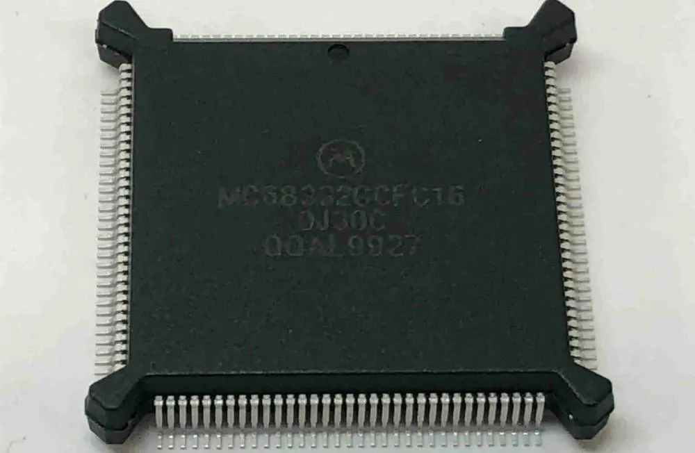
What is a QFP? A QFP is a surface-mounted IC (integrated circuit) package having “gull-wing” like leads extending on either side of their four edges. Generally, these packages are extensively utilized by very large-scale and large-scale ICs. The number of pins utilized in this technology is more than one hundred, making it pretty efficient. QFP technology smoothens IC operations. It also makes these packages pretty reliable when it comes to packaging the central processing unit (CPU).

QFPs have small parasitic parameters, and they are also pretty tiny in size. These features make them suitable for higher frequency applications.

In the manufacturing of the QFP packages, three base materials are utilized, namely:

  • Ceramic
  • Metal
  • Plastic

In terms of quantity, plastic packages take the lead. It is actually so widely used such that whenever you see a QFP package material with no label on it. Then you should automatically know that it is plastic.

QFP basics

QFPs come in two shape variations, rectangular and square:

  1. Rectangular โ€“ the number of pins that come out of each side is different due to varying lengths. One side might have more pins compared to another.
  2. Square โ€“ they have the same number of pins on each side as they have the same length.

QFP packages have two sections: the top and bottom sections. These two sections are then glued together to form a complete QFP package. QFP pins are usually bent downwards for easier connectivity to the print circuit board. The pins just touch the PCB making the soldering process pretty easy.

QFP integrated circuits vary in terms of formats and also in terms of the number of pins utilized. However, QFPs are often square, and the pin count mostly lies at around 256 or more.

By definition, a QFP with 256 pins means that it would typically have around sixty-four pins protruding on either side of the package. However, some smaller QFPs might have only thirty-two pins, which means they have eight pins on either side. In this example we are assuming that the packages are square in shape.

QFP package variations

As stated above, QFPs come in many different variations, which include:

Bumpered quad flat pack (BQFP)

These QFPs have extensions on each of their four corners. The extensions shield the leads against any mechanical damage before you solder this package onto a PCB.

One major QFP issue is how easily the lead pins get damaged or bent. And because of their fine pitch, it becomes close to impossible to repair a device having bent pins.

Bumpered Quad Flat Pack having Heat Spreaders

These QFPs utilize pin protectors positioned at the device’s corners. And on top of that, it also has heat spreaders which allow higher power levels dissipation to improve efficiency.

Ceramic Quad Flat Packages

These packages utilize ceramic which improves their quality and also their efficiency.

Fine Pitched Quad Flat Packages

These packages are QFPs with a pretty fine pin pitch just as their name dictates.

Heat Sinked Quad Flat Pack

Integrated Circuits might dissipate pretty high levels of heat, especially those which have high pin counts. Due to this heat dissipation this ICs eventually end up having high circuitry levels. The heat dissipated by this IC needs to be ejected from them for better performance. To accomplish this you must replace a couple of pins, often those found in the central part of the opposing side, with pins that are thicker. Solder these replacement pins onto a larger pad on the print circuit board with a large copper area. With this setup in place, this device can dissipate much heat away from the ICs.

Low profile Quad Flat Packages

Low-profile Quad Flat packages or simply LQFPs are based upon MQFP and QFP metrics. They are thinner, having a body thickness of only 1.44mm, which means that they can be utilized in components that have height issues.

LQFPs specs can be defined as follows:

  1. Lead โ€“frame footprint โ€“ 2.0mm
  2. Lead count โ€“ ranges from thirty-two to two hundred and fifty-six
  3. Body size โ€“ ranges from 28 x 28 millimeters to 5 x 5 millimeters
  4. Lead pitches โ€“ comes in four different variations: 0.3, 0.4, 0.5 and 0.65mm

Metric Quad Flat Packages

These QFPs have their measurements defined in terms of metric dimensions. Normal QFPs, on the other hand, utilize imperial measurements. They define pin spacing and et cetera in terms of imperial dimensions rather than metric dimensions.

Plastic Quad Flat Packages

These packages are built out of plastic.

Thin Quad Flat packages

TQFPs are a low-profile QPF variation. They have a height of 1mm and a standard lead-frame footprint of 2.0mm. These packages are manufactured using plastic.

Issues to take note of when dealing with QFPs

qfp Packagesย 

Quad Flat Package damage

QFP pins are pretty small, plus they have small spacings. Their positioning and size makes them vulnerable to damage that is hard to fix. To make sure that these devices are safe, you should store them carefully to minimize the chances of damage. If you plan to transport them, we recommend that you pack them on special ‘waffle’ packaging for adequate protection.

Print Circuit Board density track

The number of pins that a QFP can accommodate means that you should take a lot of care when designing PCBs. If you get clumsy when designing your PCB, then you might encounter track density challenges around the QFP. So careful designing and routing are pretty essential to ensure that you do not violate any designing rule.

Advantages of using QFP

  1. You can utilize sockets
  2. It uses mature technology

Square QFP packages are pretty attractive to a lot of users. They bear one significant advantage that sets them apart from rectangular QFPs:

  • They let the QFP package bear high density compared to rectangular packages

Disadvantages

  1. These devices have a 500MHz I/O limit
  2. Not enough input/output complex chips

Since we stated one significant advantage of using square QFP packages, how about a disadvantage to even things out:

  • During transportation, these QFPs are damaged easily compared to rectangular packages

QFP PCB Assembly

For QFP-PCB assembly, follow the following procedure:

Solder paste stencil

Apply soldering paste onto the PCB metal pad by stencil printing. TO determine the soldering paste volume to use, you should check on the stencil thickness and the stencil aperture. Note that excessive soldering paste causes solder bridging. On the other hand little soldering paste reduces solder spreading. The measurement should hence be pretty accurate.

Solder paste

Solder paste (PB-free) is composed of some type of SnAgCu alloy. Particle size of this alloy must be suitable for solder-stencil apertures dimensions printing.

It would be best to utilize type 4 pastes for this procedure as they are more effective. Also, note that soldering paste is sensitive to humidity, temperature, and age.

Placement

Self-alignment that occurs because of the surface tension of the liquid solder support reliable solder joint formation. However, you still need to place the component carefully. Setting the package manually is not recommended. Instead, we recommend that you utilize a pick and place machine to ensure accuracy each time.

Reflow Soldering

In print circuit board QFP assembly, you can utilize a force convection oven for reflow soldering. Soldering your QFP in an atmosphere full of nitrogen can improve the solder jointโ€™s quality. However, this is not necessary for the creation of reliable joints.

QFP solder joint temperature can be affected by a couple of things:

  1. Its position on the PCB
  2. It’s surrounding
  3. The PCB thickness

For power packages whereby shortage and leakage current below the QFP are a factor to, you should solder using less flux spread.

Remember to follow the manufacturer’s guidelines when soldering to achieve an optimal output.

Now let us advance on to the next section, where we will compare QFPs and QFNs to identify the difference between the two:

Differences between QFP and QFN

Here are some differences that will help you differentiate between these two devices.

Lead difference

QFN โ€“ Leads extends on all four sides of the QFN package

QFP โ€“ Leads extends out in a gull-wing shape or an L-shape

Assembly portion difference

QFN โ€“ The average footing for QFN packages occurs during the PCB assembly procedure

QFP โ€“ Lead form has an excellent base for the QFP package even during the PCB assembly procedure

Pin difference

QFN โ€“ These packages have only eight pins in total, plus a thermal pad

QFP โ€“ These packages, on the other hand, have multiple pins ranging from eight pins per side to seventy pins per side

Conclusion

Quad flat No-lead packages and Quad flat packages are both pretty impressive devices. However, these two are not one of a kind. We hope this article has shed light upon any questions you might have had regarding QFPs and QFNs and their differences. With the knowledge gained from this article, you can make great IC choices without breaking a sweat.

What is .PRO File ?

.PRO Files

The .pro file majorly belongs to Punchโ€™s Home and Landscape Design Pro. This file extension is the main type used in storing a buildingโ€™s 3D models. Also, it is useful in the interior designs that are created with the use of IMSIโ€™s TurboFloorPlan.

The .PRO file has different contents. These include foundation, building layouts/floors, electrical plans, plumbing and landscape. You can save unfinished designs to a .PRO file and then resume it later. PUNCHโ€™s 3D home design tool called Professional Home Design utilizes the .pro file. It helps to store its projects. This type of project may involve the floor layout, foundation, the deck. It also involves other objects such as a homeโ€™s roofing design.

Furthermore, KiCad, which is a program known to automate designs for electronic circuits. This makes use of the .pro file to store any project. Also, ProPresenter, which is a software that helps in presenting and sequencing worship songs, makes use of .pro files in storing different video and audio files, which are mostly worship songs. Also, the .pro file is useful in storing projects that are created with the use of Qt. Qt is a package that develops applications.

How Can You Open .PRO Files?

To open .pro files, you will need reliable software such as Home and Landscape Design Pro. Furthermore, without making use of the right software, you will get a message from Windows.  Examples are โ€œWindows failed to open this fileโ€ or other related alerts from Android, iPhone, or Mac.

Also, if you fail to open the .pro file the right way, you can long-press or right-click the file. Next, select โ€œOpen With.โ€ Once it opens, choose the application you will love to use. Also, you can display the .pro file in your browser directly.

What Programs Can You Use in Opening and Converting PRO Files?

Home and Landscape Design Pro

This software was developed by Punch. They are usually called the 3d images of the Home and Landscape Design Pro. This is because it is majorly used or created by using this software.

Chord Pro

This is by Mussoft. This program is a classic one, which allows users to edit, create, print, and display the lyrics of songs. These include piano chords or associated guitar in a form of graphical representation.

Also, you can store music notation. This is created with the help of Chord Pro by making use of file extensions that are arbitrary. These include CHPRO, PRO, CHORD, and more. The classification of the file format is under โ€œDataโ€.

Ape

This hardware was created by Steven Tucker. It is capable of imitating Atari computers of 8-bit. Also, the main format for the disk-image that is utilized by the operating systems of Atari for the APE emulator is the PRO. The classification of the file format is under โ€œSystem.โ€

Euphoria

This programming language is an interpreted one for computers that run using MS-DOS, FreeBSD, Linux, and Windows. Furthermore, on computers using Windows, Euphoria makes use of PRO files in storing color highlighting data. Also, the classification of the file format is under โ€œDeveloper.โ€

Creo Elements/Pro

This is a well-known Windows-based CAM, CAE, and CAD modeling program from 3D, with PTC known as the developer. Furthermore, this program is majorly useful in the manufacturing and engineering sectors. Also, GUI elements, settings, skins, themes, as well as other Creo Elements/Pro configurations that are stored in the .PRO files. The classification of the file format is under โ€œSettingsโ€.

HTMLtool

This was developed by Lorenz Graf. It is a reliable and versatile code editor that helps in the editing and creation of the source code for JavaScript, ASP, CCSS, HTML, and more. Also, the program provides better features such as FTP client, spell checker, and syntax highlighting.

Any project file that is created using the HTML tool is stored in the .pro file. The classification of the file format is under โ€œDeveloper.โ€

Fast-Talk

This is a top and classic software that allows users to perform phonetic searches that are parallel to the usual spoken audio. Furthermore, this program has the ability to search, as well as retrieve a word or string very quickly. The pronunciation files that are useful in determining the phonemes sequence in any search tem have .pro file extension. The classification of the file format is under โ€œAudioโ€.

Pagis Pro

Xerox developed this. Pagis Pro serves as a suite for color scanning. This allows users to view, scan, copy, fax, or edit electronic photos and documents. Also, this is done on Windows NT 4.0, 98, and 95 computers. These graphics are stored in the .pro files. The classification of the file format is under โ€œRaster Image.โ€

Infinity Game Engine

BioWare is credited for this. This is a kit for software development. It helps in creating role-playing isometric video games. Furthermore, this package was useful in creating video games such as Baldurโ€™s Gate. There are game data like descriptions for the projectile type, which the Infinity Game Engine created and saved in the .pro file. The classification of the file format is under โ€œGameโ€.

PROLOG

This is a form of programming language. PROLOG is majorly useful in artificial intelligence and computational linguistics. Also, the initial release of this program happened back in 1972. The source code that was written in PROLOG language was stored in the files having P, PL, or PRO file extensions. The classification of the file format is under โ€œDeveloper.โ€

Qt

This is a C++ application framework for development. Also, it includes tools for possible cross-platform internationalization and development.

Also, this .pro file has information like stylesheets, translation sources, and resource files. These are necessary for the compilation of a Qt application by making use of the command โ€œqmake.โ€ The classification of the file format is under โ€œSettingsโ€.

Conclusion

We hope we have been able to explain what the .pro file is all about. Also, we have given you several ways, as well as softwares that will help you open the .pro file. If you have any more questions bothering you, please reach out to us here.

Taconic RF-35A2 Ultra Low Loss Power Amplifier Substrate

Taconic RF-35A2 Ultra pcb

Power amplifiers are the heart of most modern wireless communication systems. Taconic RF-35A2 PCBs is a particular type that can handle these tasks admirably. These devices use a combination of amplification stages, crossovers, and filters. They provide crystal clear audio at high output power levels. As a result, they minimize losses in the process.

Employing their designed semiconductors provides impressive power transfer levels for minimal power losses.

The RF-35A2 is also very circuit efficient and efficient in power dissipation.

The RF-35A2 has a power output of 1.6 W per channel. Its internal LNA, low noise amplifier, and balun make the amplifier capable of delivering up to 3W of audio into a 10MHz channel at a minimum RF input level of -50dBm.

Since the RF-35A2 is both power and circuit-efficient, it consumes very little energy and produces very little heat. The RF-35A2 has a typical idle current of only 1.5mA. Its peak current consumption is 4.5A RMS at 4W output power. This translates to a peak current consumption of 5.3A with an output of 8W into an 8-ohm load.

Materials

Companies like RayMing PCB and Assembly make the RF-35A2. They use a mixture of standard and specialized materials. Most of them are Taconic-made. One can construct the PCB from either FR4 or Rogers 4003 material. The former is more common for power amplifiers due to its stiffness and durability. Other components include MELF resistors. They are extremely small yet provide the same performance as any other resistor.

The RF-35A2 power amplifier can easily remove the substrate from the PCB. It uses a simple Phillips screwdriver. It makes it easy to repair damaged electronic devices.

The substrate can dissipate heat generated by the components. It uses a series of channels beneath the surface of the PCB.

The RF-35A2 works best with Taconic’s TBO-03 heat sink. It improves the amplifier’s thermal dissipation capabilities.

As for connectors on miniaturized devices, many manufacturers use surface mount connectors. They do this to save space and reduce costs. However, this causes signal degradation due to a steep rise in input capacitance. To remedy this, the RF-35A2 uses an IPC-A panel mount connector with a high input capacitance value of 0.025pF.

PCB Layout

Like most Taconic designs, the layout of the RF-35A2 PCB is extremely simple. The entire assembly consists of three main sections. The first section contains the amplification stages, lowpass filters, and volume controls on one side. In contrast, we place highpass filters and output stages on the other.

We use a secondary substrate to support the power LED, DC power jack, and other components necessary for the operation of the amplifier. They place these components to remove the entire assembly using a simple Phillips screwdriver. This feature allows for easy repair and modification of existing devices.

Several traces run along the top edge of the circuit board. We can use them to provide additional components to increase performance or lower costs.

The RF-35A2 is also quite resistant to mechanical damage. For instance, we mount the components on the amplifier in a very sturdy manner. One can operate it safely without worrying about its stability.

The RF-35A2’s PCB uses Taconic’s components to add reliability or reduce cost. This is especially true of resistors and capacitors. Specifically, we select them for their high quality and low cost.

Performance and Use

The RF-35A2 manufacturing process is straightforward. It allows for easy customization and modification. This makes it perfect for use in various other electronic devicesโ€”for example, cell phones or wireless routers.

Unlike most power amplifiers, the RF-35A2 can operate for long periods without fail. It gives reliable performance in the harshest environments. It can continue operating even when the amplifier’s temperature reaches 40 ยฐC.

The RF-35A2 is also extremely efficient, and it consumes very little energy while providing high output power.

The RF-35A2’s efficiency and maximum power output are helpful in several different applications. It includes wireless routers and large-scale paging systems.

The RF-35A2 provides high-quality audio and high output levels. So, we often use it in paging systems that cover large areas such as city blocks or office buildings.

In addition to its use in audio amplifiers, the RF-35A2 is also very commonly used as an RF power amplifier in a range of other applications.

Additionally, we often use it for analog satellite systems. It amplifies the frequency-modulated (FM) signal from the LNB. We can also find it in other transmitters. For instance, those used to relay emergency alerts or data from weather satellites.

Test Results

All RF-35A2 power amplifiers underwent testing using an Agilent 8310A spectrum analyzer. They measured the output powers of each amplifier over a wide range of frequencies. It included typical MELF bias voltages and output levels ranging from 11W to 150W converted to approximately 20Vrms. They took all measurements with the amplifier held at ambient temperature. It had free air within the space between the device and the analyzer.

The RF-35A2 was very reliable and stable in most test conditions. It maintained high output levels even with very low bias voltages (below 0.5V). It produced significantly higher output powers at high bias voltages (above 0.8V).

The RF-35A2’s efficiency ranges from an excellent 78% at 8W into 1kฮฉ of load resistance to an exceptional 93% at 150W into 10ฮฉ of load resistance. In most applications, we will drive the RF-35A2 closer to 0.25V than 0.5V. Still, the amplifier’s output levels were slightly higher at a bias of 0.5V than at a bias of 0.25V. They showed no signs of instability or degradation in performance over extended periods.

Taconic found that the RF-35A2 performed as expected in stability and efficiency even when used with very low bias voltages.

Benefits of using the Taconic RF-35A2 PCB

1. Low cost

We fabricate the RF-35A2 using a very efficient process. The process incorporates several Taconic quality components that cost less. In addition, its reliable performance levels also allow for higher output power at lower drive voltages. It further reduces costs in both the short term and long term.

The low manufacturing cost also gives users flexibility in choosing different amplifiers.

2. Low loss properties

The RF-35A2’s efficiency and loss level also contribute to its low manufacturing cost. The amplifier’s high efficiency allows for increased output levels at lower bias voltages. It reduces cost in the short term by enabling users to use currents that are less than those of alternative devices. In addition, the RF-35A2’s low loss levels allow for greater output power at higher bias voltages. This translates into even higher efficiency and lower long-term cost.

3. DK tolerance of +/- 0.05

The RF-35A2’s onboard DK tolerance of +/- 0.05V reduces long-term costs. Each stage of the RF-35A2 can operate within the device’s specified operating range. This ensures that its performance will be consistent regardless of voltage and temperature. Since the RF-35A2 operates within a very narrow voltage range, we use it in applications with fluctuations in operating power. This allows for more reliable performance and greater ease of operation.

4. Homogeneous DK

The RF-35A2’s common ko bias increases output power at lower drive and bias voltages. Since all amplifier stages can operate within a single voltage range, the Taconic amplifier will produce the same supply voltage throughout its entire life span.

5. Excellent peel strength

Since the RF-35A2 uses a high-quality epoxy resin, its peel strength is extreme. This makes it easier to install and remove, which results in lower installation costs. In addition, strong peel strength also eliminates the need for adhesives. This, in turn, helps strengthen the device and increase its reliability.

6. Ease of drilling

Since the RF-35A2 uses a common drilling method, it is easier to install than other power amplifiers. The RF-35A2’s design allows for the use of a full range of common drilling brands and sizes. Since we can easily modify and repair the device, it helps increase its lifespan and prevent problems with them in the future.

Applications

The RF-35A2 can be helpful in a variety of consumer electronic devices. LED lights, wireless transmitters, and RFID chips are a few examples of the many types of devices that you would enjoy.

Since the RF-35A2’s performance levels are excellent even at higher drive voltages, it is also a good choice for applications requiring high output power levels and high output currents.

1. Power amplifiers:

Although the RF-35A2 has a low bias, its DK tolerance ensures that it performs well under more rigorous testing conditions. This translates into more reliable performance at higher output power levels. It is ideal for many applications.

2. Filters/couplers: The RF-35A2’s forward gain and f>10dB return loss ensure that it is an excellent choice for use in filters and couplers.

3. High-speed digital:

The RF-35A2 serves as an effective component in high-speed digital applications.

4. Multilayer:

The RF-35A2’s excellent high-frequency properties make it a good candidate for multilayer PCBs.

5. Passive components: RF-35A2 is an excellent candidate for use as a resistor, inductor, and capacitor die.

6. Wireless antennas:

The RF-35A2’s high efficiency makes it a suitable recipient for wireless antennas.

The RF-35A2 cannot replace any of the current products on the market. However, it offers manufacturers another option in high-performance power amplifiers.

The main drawbacks of the RF-35A2 are that it uses a higher bias voltage than many other devices. Its fmax is lower than that of some other products.

Conclusion

The RF-35A2 is relatively robust. It is also a straightforward wireless power amplifier. It can provide excellent performance at a low cost.

Taconic’s RF-35A2 is a particularly low-cost and efficient power amplifier. It is suitable for many devices, such as cell phones and wireless routers. Since one can modify or repair the board, it helps increase its lifespan and prevent problems with them in the future.

All the power amplifiers tested performed admirably under rigorous testing conditions. The RF-35A2, however, had the lowest power loss levels of all the devices and was only out-performed by a few others. The low loss design of this amplifier makes it ideal for applications where it needs high power output.

What is DRC PCBย ?

drc pcb

PCB manufacturing and design is a very complex process. This process involves mounting and connecting several components on a PCB. Therefore, it is crucial to have a check on this process. One of the best ways to ensure an error-free PCB design and manufacturing is through a design rule check (DRC).

Early detection of errors in the design stage will prevent further errors. PCB design rule check is crucial in ensuring the fabrication of quality boards. DRC errors in PCB design are very common. Also, it is important to detect these errors and correct them on time.

What is DRC PCB?

DRC PCB is a set of rules adopted by PCB designers. It helps to verify their schematic matches the manufacturing considerations of a board. With a DRC, a design can verify that the schematic and layout reflects the design margins you are incorporating in a design.

PCB design rule check is widely adopted to detect mismatches and errors. These errors include traces and widths in a PCB design. PCB designers use software to design the layout of a circuit board. Every PCB manufacturer works with a set of rules that describes various parameters. Some of the parameters specified are the minimum size of vias and the spacing between each line.

Once a PCB manufacturer gets a design, it carries out a DRC test. This test helps to verify that the design submitted matches their published standard. If there is any mismatch, the DRC PCB detects them. The designer will have to update the layout or design according to the right standards.

However, the PCB design rule check varies among manufacturers. Before PCB users submit a design to the manufacturer, they should check the DRC PCB.

PCB DRC Rules

There are a set of rules that help to detect several mistakes. These rules include:

Vertical plane change rule

Trace routing from one layer to another is a design practice that accommodates dense PCB layout. However, it is important to minimize the risk of mode radiation. Also, this rule detects the transitioning of signals from one layer to another. Also, it detects how stitching vias or stitching capacitors are placed near nets.

Crosstalk coupling rule

This rule helps to detect areas where unwanted crosstalk appears on sensitive nets. Also, crosstalk can result in functionality errors. Furthermore, it can be difficult to detect this problem manually on a PCB.

Filer placement rule

The filter placement rule detects any filter close to the pins of a connector. Filters minimize noise that may occur on a connector. Therefore, this helps to prevent radiation and shield sensitive signals. The misplacement or absence of filters can result in EMI failures.

Decoupling capacitor placement rule

It is important your PCB designs meet the demands of every component. Checking the placement of decoupling capacitors on every net is important. However, this can be time-consuming if you are checking manually. The decoupling capacitor placement rule identifies all decoupling capacitors placed improperly.

Signal supply rule

This identifies discontinuities between the supply planes of an integrated component and the reference plane of connected traces. Any violation as regards this can result in EMI failures and EMI radiation.

Ground/power width rule

This rule detects ground traces and narrow traces that arenโ€™t wide enough. If these traces arenโ€™t wide enough, there can be an insufficient current on the net. Therefore, this can result in several problems. Some of these problems include unnecessary heat production. Also, it can cause an inadequate power supply to components.

How DRCs can Reduce Board Re-spins

Sometimes, PCB designs experience re-spins. This will cause a significant cost for each re-spin. Therefore, electrical DRC via pcb capabilities make sure designs meet specific requirements. This can be achieved by reducing and getting rid of possible re-spins. These checks include signal integrity, electromagnetic interference, and safety checks.

Checking for Differential Symmetry with DRC

A PCB design may comprise several differential pairs. This includes 100ohm and 50ohm differential impedance. Such differential pairs are inside the constraint manager of the layout tool within a separate constraint class. The constraint class within the PCB tool will be automatically defined within the DRC tool. This is because of the tight integration between DRC and layout. Therefore, designers can make an object list from the constraint class. This enables them to choose to manage the next rule on the two differential nets.

Differential impedance traces should be properly designed for great functionality. However, there are properties that determine this functionality. They include the position of the pairs, spacing, and symmetry in the length. Therefore, the differential pair rule helps to check the consistency of these properties.

PCB designers can specify rule parameters like maximum and minimum allowable trace length. This is because the tested differential traces have particular differential impedance. Therefore, the PCB DRC helps to customize every rule for individual design parameters.

Online DRC PCB Tools

Altium Designer

This is a great online tool for PCB design rule check. Altium designer is a powerful tool that checks the integrity of a PCB design. Also, it features various options for checking PCB designs.

EasyEDA

EasyEDA offers you a DRC function. This online tool will allow you to detect several errors. Also, this tool runs on macOS, Windows, and Linux. It is a reliable tool that features various component libraries. Also, this online tool has a cloud-based feature that allows several users to work on a similar project simultaneously.

kiCad EDA

This is one of the most reliable PCB design tools that help you to create a high-quality PCB.  Furthermore, KiCad EDA runs on macOS, Windows, and Linux. Also, it offers all necessary files for PCB designs. This easy-to-install online tool is very easy to use.

What is Depth Control Routing PCB?

Depth control routing PCB is the partial routing in PCB manufacturing with a level elevation within PCB. This helps to support a high end market. Depth control routing in PCB allows the processing of bent PCBs and complex designs with great precision. Depth control routing has great benefits in a PCB assembly.

Conclusion

DRC errors in PCB design are very common. Therefore, PCB design rule check is crucial to fabricating high-quality boards. Therefore, manufacturers must ensure, they adopt this rule in their fabrication processes.

Top 10 silicon wafer manufacturing companies in the world

silicon wafer manufacturing

Silicon wafers are the foundation of modern electronics. So, they create a sub-microscopic layer that. It includes the integrated circuits that are now ubiquitous in our daily lives. Nowadays, there is an increasing need for faster silicon wafer manufacturing. So, companies across the globe have arisen to meet this demand.

Silicon is one of the essential materials for every electronic product on Earth. As a result, we must produce silicon wafers with precision and efficiency. But silicon wafers are new compared to their more cousins in the industry. The first significant use of silicon in electronics did not occur until after World War 2.

But, the wafers that we are familiar with today have been in mass production for almost 50 years.

What is a Silicon Wafer?

A silicon wafer consists of a single crystal on a very thin silicon layer. So, we can arrange them in many different ways. The wafers come in many sizes. As a result, some are more valuable than others. They are often helpful as the base material. As a result, they help create modern processors, memory chips and integrated circuits (ICs).

The type of wafer you use depends on your specific needs and industry. The most common type of silicon wafer is the single-crystal silicon wafer. Additionally, there are three primary forms of the single-crystal silicon wafer:

Type A โ€“ This waferโ€™s most used type has a very high purity of 99.999%. We use it in high-performance computer memory chips, cell phones, and digital cameras. They are also essential in other devices that need a high degree of density and function.

Type B is more challenging to produce than type A due to its high purity value. But, we use it in high-resolution colour memory chips and sensor applications. These are applications that need very high performance at a low operating temperature.

Type C โ€“ A cheaper alternative to type B, this wafer has a purity of less than 99.999% but still meets most end-uses. We use it to manufacture logic chips. They provide functionality in integrated circuits. As a result, it enables computers and iPhones to send data and perform calculations.

History

To understand the importance of silicon wafers, we must look at the history of the material. The first silicon-based electronic devices came out in 1882. Heinrich Hertz from Germany and Nikola Tesla from New York City were the inventors. They used a crude form of semiconductor technology to show the existence of radio waves. It was later called Hertz. The wave of energy produced by a spark between two electrodes consisted of electromagnetic radiation. But these waves are not visible to the human eye. This finding was a rudimentary form of semiconductor technology. So, these scientists used non-metallic conductors to create the energetic wave.

But these scientists, who laid the foundation for the electronics field, did not stop there. Hertz and Tesla continued to experiment with this new technology. Tesla invented what we now know as the Tesla Coil. It is a device used to generate electromagnetic waves at higher frequencies than Hertz. These waves could then move wirelessly through the air without cables.

In 1905, Albert Einstein published his famous paper on โ€œDoes the Inertia of a Body Depend Upon Its Energy Content?โ€.

Today, Einsteinโ€™s paper is one of the essential publications in physics. It is the foundation for modern atomic theory. But at the time, Einsteinโ€™s work was not well received. However, the concepts were historically significant. So, to further understand his theories, Einstein decided that he needed a better experimental platform to test them on. He believed that we could achieve this by creating a unique device. This device would be capable of measuring small changes in electromagnetic mass.

Top 10 Silicon Wafer manufacturing companies

silicon wafer price

Hemlock Semiconductor Corporation

Hemlock Semiconductor Corporation is an American semiconductor foundry. It specializes in creating high-density and high-performance logic devices for microprocessors. Hemlock also works with digital signal processors and graphics processing unit markets. It came into existence in 1990, and its headquarters are in Honolulu, Hawaii. Hemlock also has offices in Tokyo, Japan and Taipei, Taiwan. The company is in the top ten silicon wafer manufacturers globally. However, the ranking depends on its production capacity. Hemlock Semiconductor Corporation produces over 45,000 silicon wafers per month. It has a total production area of over 75,000 square feet.

LANCO

LANCO is a corporation known for its production and sales of silicon wafers. It had its headquarters in Nara Prefecture, Japan. LANCO produces several products. They include:

  • semiconductor devise manufacturing tools
  • grinding machines
  • polishing machines
  • ion implantation machines
  • ion implanters
  • electrical discharge machines

It started operations in 1971, and it is one of the worldโ€™s top ten silicon wafer manufacturers.

LANCO manufactures high-quality polysilicon wafers used in electronics, telecommunications, and other industries. It started as a small company. However, it has become one of the worldโ€™s largest producers of dielectric materials by volume. LANCO operates biennially at over 200 facilities worldwide. It has a total production area of over 1.4 million square meters (15 million square feet).

Elkem

Elkem is a Norwegian company that specializes in silicon wafer manufacturing. Based in Trondheim, they produce semiconductors. They also make other materials used in electronics and the microelectronic industry. Ole F. Christiansen founded it in 1947 under the name Elektronikk og Materiell. It led to the name Elkem. Additionally, they have one of the largest global production capacities of silicon wafers/. As a result, they outdo some of the leading silicon wafer manufacturing companies globally.

Elkem operates with a total production area of around 3 million square meters. So, it has a production capacity of almost 1.5 million silicon wafers per month. Their primary services include developing, fabrication, and sales of high-performance materials. In addition, we use them to produce cutting-edge products in the electronics industry. For example, they have LEDs, solar cells and semiconductor devices.

MEMC Electronic Materials

MEMC Electronic Materials is a company headquartered in Nanjing, China. It started in 1992. So, it is a top ten silicon wafer manufacturer globally. As a result, this depends on its annual production capacity. MEMC produces high-purity polysilicon wafers. This helps to create DRAM memories, logic chips and other electronic devices. Also, MEMC engages in the research and development of materials. We use them to make semiconductor devices and high-quality silicon material. They are essential for computer memory chips.

This is a global pioneer in developing, producing, and selling high-quality silicon wafers. It also provides a variety of other semiconductor materials to clients worldwide. It maintains production facilities in 11 different locations around the globe. Most of them are in China, Spain, Germany, and the United States. MEMC has a production area of about 310 million square meters.

Okmetic

Okmetic is a Silicon Wafer manufacturer. It produces high-purity silicon wafers used to manufacture analogue and digital electronics. Okmetic started operations in Germany in 1992. Okmetic initially operated under VBK Silicon. Then Semiconductor Business Europe (SBE) acquired it in 1995. It then changed its name to Okmetic. It is an initialism for โ€œOK,โ€ the German word โ€œOKโ€.

Novellus Systems Group finally acquired SBE in 1999. This technology company design develops and manufactures a variety of silicon wafers. So, we use them to fabricate digital and analogue semiconductors. Okmetic operates with a total production area of over 1 million square meters. They have more than 1000 workers worldwide. They are one of the worldโ€™s top silicon wafer manufacturers in production capacity.

PV Crystalox Solar

The PV Crystalox Solar is a silicon crystal manufacturer, and its headquarters are in the Netherlands. They specialize in producing silicon wafers to supply to the solar photovoltaic industry. Founded in 1978, we often refer to PV Crystalox Solar as โ€œThe Dutch Silicon Valleyโ€. This is because it has high-quality silicon wafers. In addition, they are suppliers of solar cell manufacturers like CIGS Cell and others.

PV Crystalox Solar has a total production area of around 200,000 square meters (2.3 million square feet). They have a current annual production capacity of 2 million silicon wafers. Also, they operate at over 20 facilities around the globe.

It produces multi crystalline silicon ingots and wafers, making crystalline silicon solar cells. PV Crystalox Solar utilizes the latest technology in silicon wafer manufacturing. As a result, they include high-temperature vacuum processing and high-purity, rapid temperature annealing processes. It also has a comprehensive quality control infrastructure. This ensures its products are always of the highest quality.

Shin-Etsu Chemical

Founded in 1931, it was only focusing on semiconductor materials. However, the company has become Japanโ€™s second-largest silicon wafer manufacturer. They operate with a total production area of over 750,000 square meters.

Shin-Etsu Chemical is a company that specializes in the production of semiconductor materials. They are one of the top silicon wafer manufacturers worldwide. Their products also include quartz, zinc oxide, and hydrogen fluoride.

Shin-Etsu Chemical is a Japanese company. It produces silicon wafers used in the semiconductor industry. They are mostly known for being one of the largest silicon wafers producers globally. We use them for NAND Flash memory manufacturers. Some of them include Vertec Company, Rayming PCB & Assembly, Renesas Electronics, and other Japanese companies.

Siltronic

Siltronic is a global leader in producing high-purity, silicon photovoltaic (SiPV) devices. The company started in 1963 and had a total production area of around 2 million square meters. They have almost 2 million semiconductor wafers per month. This is equal to about 100 million silicon wafers per year.

Siltronic manufactures and distributes a variety of different semiconductor products. They include:

  • Single-crystal silicon ingots and wafers
  • Multicrystalline silicon ingots and wafers
  • Standard-grade solar cells
  • Ultra-high-purity silicon ingots and wafers

They also produce high-quality semiconductor devices for a variety of different applications.

This company has one of the largest production capacities for solar cells globally. They have manufacturing facilities around the globe. But, global wafer Siltronic has its headquarters in Germany. They operate with a global workforce of almost 4,000 employees.

Mitsubishi / Sumitomo Sumco Silicon

silicon wafer production by country

Mitsubishi Silicon Corporation is a Japanese company. So, they produce silicon wafers used to manufacture solar panels and semiconductor chips. The company started in 1949. It specializes in delivering high-quality, multicrystalline silicon ingots and wafers. For use in the solar photovoltaic industry.

Mitsubishi operates with a total production area of about 1 million square meters. It consists of several different production facilities around Japan. They also operate with an entire workforce of over 7,500 employees.

Mitsubishi Sumitomo Sumco Silicon is a multinational corporation. So, it produces high-purity silicon wafers used to manufacture solar panels and semiconductor chips. The company started in 1973, and they have their headquarters in Japan.

LDK Solar

LDK Solar is a silicon wafer producer. It specializes in silicon wafers for the solar photovoltaic industry. Founded in 1992, Its headquarters are in China. LDK Solar is one of the largest crystalline silicon wafers used in solar panels.

LDK Solar has a total production area of about 500,000 square meters. They have a current annual production capacity of 1 million silicon wafers. In addition, they produce silicon wafers to manufacture solar panels.

LDK Solar is the largest crystalline silicon wafers used to manufacture solar cells. It has a production capacity of around 1 million wafers per month.

Silicon Wafer Production Process

Silicon wafer production begins by melting purified silicon. Then, we use a heat gun or a furnace, heating, and high-temperature annealing it.

They transfer each silicon wafer from the furnace to a tool called an etch stencil. So, it etches it to remove the unwanted silicon material. The remaining part at the bottom of the etch stencil is the seed layer. Finally, we polish it to expose the silicon ingotโ€™s crystal face. Below are the preparation and production details.

Preparation of the Silicon Wafer Media

The purpose of preparing the silicon wafer media is to remove the unwanted silicon material. We find these materials on the seed layer. As a result, we refer to this process as silicon wafer production. It starts by vapor removing the unwanted silicon material. Then, we do this by heating it in an oven enough to complete this process.

Crystal Growth and Wafer Slicing Process:

We place single crystal seeds on a rotating wafer carrier to grow the crystal silicon on the seed layer. After the crystal is grown, itโ€™s cut into thin slices and sent for testing and packaging.

Thickness Sorting:

We send the wafer to be thickness-sorted. Then it is ready for the crystallization process.

Lapping & Etching Processes:

The next step in the wafer wafering is to lap and etch the wafers. Then we do the lapping by polishing the surfaces of the silicon wafers. In this step, we use a lapping machine called a lap-polisher.

Thickness Sorting and Flatness Checking:

The wafers of the same size and flatness are then packaged and sent to be ready for the following process.

Polishing Process:

The next step in silicon wafer production is to polish the silicon wafers. Then, the polishing process uses polishing processes like pickle and shot blast.

Final Dimensional and Electrical Properties Qualification:

The silicon wafers go for testing and qualification. We do the final dimensional and electrical properties qualification. This is to determine the quality of the silicon wafers.

Silicon Wafer Processing Steps

The different processing steps help put the wafers through before they are ready for the following process. First, the wafers pass through various processing steps. They include silicon wafer cutting, testing, slicing and polishing.

In the case of its use in solar panels, we measure monocrystalline Silicon in Angstrom units. In other words, we measure monocrystalline silicon depending on its approximate molecular weight. Monocrystalline Silicon has a โ€œgrain sizeโ€ of approximately one micron. It means itโ€™s a layer of crystallized silicon that looks like a needle.

Fabrication:

The silicon wafers go for fabrication after the crystal growth. Then the wafer slicing process follows. The fabrication process includes the following steps:

Monocrystalline Silicon wafers are first sliced into thin silicon ingots then polished. We then coat the rough surface of each silicon ingot with a layer of photoresist. Then we expose them to light through a patterned mask.

Diffusion:

The patterned mask comes out, and it is now time for the diffusion process. First, we expose the silicon wafers to a solution of nitrogen and hydrogen gases. Then the hydrogen molecules diffuse into the silicon lattice. As a result, then they bond to the silicon surface. The process stops when thereโ€™s no more diffusion after several hours of exposure. This depends on some specific levels of hydrogen.

Coat-Bake:

After exposing the silicon wafers to the hydrogen gas for several hours, they bake in an oven for several hours. This process aims to remove the silicon wafers from the solution, which can be harmful. And after that, the silicon wafers go for coating with a layer of SiO. Finally, we then passivate it with a chemical called HF.

Align:

The next step in the fabrication process is to align the wafers. The wafers then move to the aligning machine. First, it aligns them by making them spin around and line up. After that, the machine polishes and metallizes them.

Develop:

After aligning and polishing the wafers, the machine develops them. Then, they go through a โ€œmagnetic coatingโ€ process.

Dry etch:

The wafers then go dry carving before another round of polishing and metallizing. After that, we expose them to a high-temperature annealing process. This gets rid of any remaining hydrogen molecules.

Wet etch & clean:

When the wafers are ready to go through the wet etch process, we first clean them with an HF chemical. The wafers are then exposed to WF sublimation gas and then sent for annealing by polishing it twice.

We saw silicon wafers into diamond-shaped pieces known as โ€œlumpsโ€ for this process. After that, we call the process sheet-cutting. We do it using a machine, which cuts the sheets from the sheet of the silicon wafer.

Photolithography:

The next step is to apply thin photoresist layers to the silicon wafer lumps. The idea is to cover the upper part of the silicon wafer with a thin photoresist layer. Then, we expose it to a patterned mask.

Implant / Masking Steps:

The next step is to expose it to a specific set of X-ray beams. Finally, we project the X-ray beams through a patterned mask. This creates a thin photoresist layer on each silicon wafer.

Die Attach / Wire Bond:

We expose the wafers to the X-ray beams through a patterned mask. Then we transferred them to a vacuum box and stored them there. Once theyโ€™re in the vacuum box, theyโ€™re ready for the die to attach and wire bond process.

Encapsulation:

The next step in the silicon wafer production process is encapsulation. This process aims to create an airtight barrier. First, this isolates the wires from the wafer. Then it protects them from oxidative gases and moisture.

Lead Finish / Trim and Form:

The wafers go for trimming and formation after encapsulation. The silicon wafers are then lead finish.

Final Testing / Shipping:

After the lead finish process, the wafers are then tested and packaged. Finally, we ship to be ready for the following process.

Criteria to Select these Top Silicon Wafer Manufacturing Companies

The essential criteria in selecting the top silicon wafer suppliers are:

Wafer Quality:

The most critical measures to choose the top silicon wafers manufacturing companies are:

-High-quality raw materials.

-Accurate dimensions of silicon wafers.

-High yield of the process.

-Long term quality about service for a fixed price.

-High-quality silicon wafers.

Wafer quality is essential in the production of solar cells. This is because they are the part that contains solar cells. The quality of the wafers will determine the final result of the finished product. It is always easy to produce something that is not good than to produce something good.

Wafer thickness:

The essential factors in selecting the top silicon wafers manufacturing companies are:

-Thickness of silicon wafer production

-Effect on panel efficiency

-Thickness guarantee

Quality of the silicon:

The essential factors in selecting the top silicon wafers manufacturing companies are:

-Carrier-to-absorber conversion efficiency.

The quality of the solar cells depends on the quality of silicon theyโ€™re made out of. So the higher level of purity in silicon, the better quality solar cells will have.

Time of the silicon wafers production:

The essential criteria in selecting the top silicon wafer manufacturing companies are:

  • -Time of the silicon wafer production.
  • -Delivery time
  • -Flexibility of delivery time.
  • -Testing time.

Cost of Energy (Capex):

The essential factors in selecting the top silicon wafers manufacturing companies are:

  • -Savings in energy cost based on saving money on solar technology
  • -Savings in energy cost based on getting more efficient solar panels

RoHS:

The essential factors in selecting the top silicon wafers manufacturing companies are:

  • -Compliance with EU RoHS standards.
  • -The solar panel manufacturer must show on their website that theyโ€™re โ€œRoHS compliantโ€

Energy Self-Sufficiency:

The essential factors in selecting the top silicon wafers manufacturing companies are:

  • -Number of goods that we can reduce using solar energy only
  • -Energy self-sufficiency

Environmental Responsibility:

The most important criteria to select the top silicon wafers manufacturing companies are:

  • -Solar manufacturers should be using eco-friendly production processes and materials

SiC Wafer Manufacturing Equipment:

The most important criteria to select the top silicon wafers manufacturing companies are:

  • -Manufacturing equipment for SiC wafer production

Conclusion

We use silicon wafers in different ways in solar cells and semiconductor lasers. For example, silicon wafers are essential to creating solar panels. This is a renewable energy source. In addition, solar panels help reduce carbon dioxide emissions, which can cause global warming.

The use of solar power has increased over the last few years. We estimate that by 2050 the total energy produced will be approximately 20% from photovoltaic systems. Solar cells can either consist of Germanium or Silicon. But the basis of all solar cells is the silicon wafer. As a result, the production of silicon wafers has increased. We expect it to increase over the following years.

Raspberry Pi 4 vs 3:What’s the Difference?

Raspberry Pi 4 vs 3

Introduction

The Raspberry Pi is a powerful, low-cost, credit card sized computer that has become a platform of choice for electronics enthusiasts, hobbyists and educators. Since the launch of the original Pi in 2012, the Raspberry Pi Foundation has steadily released newer, more capable models. The Raspberry Pi 4 Model B is the latest iteration, succeeding the very popular Raspberry Pi 3 Model B/B+.

This article provides a detailed technical comparison between the Raspberry Pi 4 vs 3 across various aspects like compute power, interfaces, multimedia capabilities and overall improvements. For users considering an upgrade from Pi 3 to Pi 4, it highlights the key differences that matter.

Raspberry Pi 4 and 3 Models Overview

The Raspberry Pi family consist of several models of single board computers with different capabilities. Here is a brief overview of the Pi 4 and 3 variants:

Raspberry Pi 4 Model B

  • 1.5GHz quad-core ARM Cortex-A72 CPU
  • 1GB, 2GB, 4GB, 8GB LPDDR4 RAM options
  • Dual-band 802.11ac wireless LAN
  • Gigabit Ethernet
  • 2x USB 3.0, 2x USB 2.0 ports
  • Dual micro-HDMI display interfaces
  • USB-C power supply

Raspberry Pi 3 Model B+

  • 1.4GHz quad-core ARM Cortex-A53 CPU
  • 1GB LPDDR2 RAM
  • 802.11n wireless LAN
  • Gigabit Ethernet
  • 4x USB 2.0 ports
  • Full-size HDMI
  • Micro-USB power

Raspberry Pi 3 Model B

  • Same as 3 B+ except:
  • 1.2GHz 64-bit quad core ARM Cortex A53 CPU
  • 802.11n wireless LAN with 150Mbps max speed
  • 10/100Mbps Ethernet

The Pi 4 brings significant upgrades over the Pi 3 family with faster processor, modern ports and extra RAM capacity.

Processing Performance Comparison

Raspberry Pi Zero Board

The Pi 4 provides a noticeable jump in processing power and speed over the Pi 3:

CPU

  • Pi 4 – 1.5GHz 4-core Cortex-A72
  • Pi 3 – 1.2GHz/1.4GHz 4-core Cortex-A53

The Pi 4’s quad-core processor is more advanced with improved pipelined execution for higher instructions per clock compared to Pi 3’s CPU.

CPU Benchmark Comparison

ModelGeekbench 5 ScorePercent Increase
Raspberry Pi 3333 Single / 1227 MultiBaseline
Raspberry Pi 4598 Single / 1990 Multi80% Single / 62% Multi increase

This translates to real-world performance boosts like:

  • Faster application and boot up times
  • Better multitasking under heavy workloads
  • Lower latency for time sensitive tasks like audio/video streaming

The Pi 4’s processor delivers excellent processing power for the price point.

Memory and Storage

The Pi 4 offers more RAM and versatile storage options:

  • Memory: 1GB/2GB/4GB/8GB LPDDR4 RAM options vs 1GB LPDDR2 for Pi 3
  • Storage Interfaces: PCIe M.2 slot for SSDs, MicroSD card for boot media

The extra memory combined with fast LPDDR4 RAM provides capacity for running bigger applications, larger datasets, and intensive workloads like image analysis with lower likelihood of slowdowns.

Onboard PCIe M.2 socket allows adding fast SSD storage instead of slower microSD cards in Pi 3.

Wired Connectivity Comparison

The Pi 4 comes with modern high-speed wired connectivity:

  • Ethernet: Gigabit Ethernet port
  • USB Ports: 2x USB 3.0, 2x USB 2.0 ports
  • USB Boot: Supported

This improves on Pi 3’s 10/100Mbps Ethernet and 4x USB 2.0 ports. The faster network and USB allows building high bandwidth data logging, media streaming, automation and IoT applications.

USB boot support allows booting the OS directly from a USB mass storage device rather than just SD cards.

Wireless Connectivity

For wireless connectivity, the Pi 4 has:

Compared to 802.11n WiFi and Bluetooth 4.2 in the Pi 3.

The modern WiFi standard in Pi 4 improves wireless network speeds and reception. Bluetooth 5.0 doubles the range and quadruples throughput over Bluetooth 4.x for whole-home coverage and better audio streaming.

Multimedia and Display Capabilities

For media, graphics and display, the Pi 4 provides:

  • Video: 4Kp60 hardware decode of H.265/HEVC video codec
  • Graphics: OpenGL ES 3.x graphics
  • Display Interfaces: Dual micro-HDMI ports supporting dual 4K displays
  • Audio: Stereo audio and USB audio class support

This is significantly improved from Pi 3’s maximum 1080p30 video playback, OpenGL ES 2.0 graphics, and single HDMI port.

Dual display output allows using the Pi 4 as a desktop computer with multiple monitors. 4K video streaming, graphics and interfacing are enabled for building media centers and gaming rigs.

Power Supply

The Pi 4 switches to a USB Type-C power supply that provides ample power delivery:

  • 5.1V 3A USB-C for a recommended 3A power supply
  • Higher stability under power surges and fluctuations
  • Can source more current allowing additional USB peripherals

The Pi 3 uses an old-style micro-USB port with a 2.5A maximum recommended supply. The new USB-C supply powers the Pi 4 properly under all use cases.

Size and Form Factor

Both Pi 4 and 3 maintain the same compact footprint and layout:

  • Dimensions of 85 x 56 x 17mm
  • Identical mounting hole patterns
  • 40-pin GPIO header located along top edge
  • Full-sized HDMI and audio jacks
  • All connectors along the boards’ edges

This consistent form factor allows using most Pi 3 cases and add-on boards with the Pi 4.

Summary of Notable Improvements in Raspberry Pi 4

  • Faster quad-core ARM Cortex-A72 processor
  • Up to 8GB RAM capacity with fast LPDDR4
  • Hardware 4K video and 3D graphics decoding
  • Higher speed USB 3.0 and Gigabit Ethernet
  • Dual-band 802.11ac wireless networking
  • Bluetooth 5.0 with longer range
  • Dual 4K display support via two micro HDMI ports
  • USB-C power supply with higher current rating
  • PCIe interface to add SSD storage

Conclusion

The Raspberry Pi 4 Model B offers a major upgrade over the Pi 3 across all areas including faster processing, additional memory, modern connectivity options and 4K ready video and graphics capabilities. It takes the Pi to the level of an entry-level desktop PC while retaining its compact single board footprint. For those needing more power for heavier workloads and bandwidth intensive applications like media centers, web servers, automation controllers etc., the Pi 4 is a significant step up. It continues the Raspberry Pi Foundation’s mission of pushing affordable technology for students, hobbyists and casual computing uses.

Frequently Asked Questions about Raspberry Pi 4 and 3

Raspberry Pi 3B
Raspberry Pi 3B

Here are some common questions when comparing the Raspberry Pi 4 and Raspberry Pi 3 models:

Q: Is the Raspberry Pi 4 compatible with Raspberry Pi 3 cases?

A: Yes, the Pi 4 has identical physical dimensions and port positions as the Pi 3 allowing reuse of most cases and enclosures.

Q: Can Pi 4 accessories like HATs be used with a Raspberry Pi 3?

A: Unfortunately no. While the Pi 4 board has the same 40-pin header, it uses different pin functionality so Pi 3 add-on boards cannot be used.

Q: How do the processors compare between Pi 3 and Pi 4?

A: The Pi 4 uses the newer 1.5GHz quad-core Cortex-A72 while Pi 3 uses the 1.2GHz or 1.4GHz quad-core Cortex-A53. The A72 has better performance per clock cycle.

Q: Does Pi 4 have built-in WiFi like Pi 3?

A: Yes, both Pi 3 and Pi 4 have on-board wireless connectivity, with Pi 4 using the latest 802.11ac WiFi standard.

Q: Can Pi 4 power external hard drives properly unlike Pi 3?

A: Yes, the higher current USB-C power supply on Pi 4 is designed to provide stable power to external USB hard drives.

What is .GPI File ?

What is .GPI File

The .GPI file format is integrated into files that comprise geographic data like the location of the user’s point of interest. GPI stands for the Garmin Point of Interest.  Garmin, a GPS company developed this file format. This company designs hardware units known as GPS Navigation. GPS Navigation is a commonly used device sync with mobile phones. Also, it helps in locating routes and directions.

For example, if the point of interest of a user is a market .GPI files will provide details about the location of that market and the closest routes to get to that market. Therefore, .GPI files are of great importance in GPS devices. You can use POIConverter software to open and view what is in these files.

Also, you can use .GPI files in fax files by Bitware. The Bitware Fax software utilizes the .GPI file suffix. As long as the Bitware Fax Program created these fax files, the .GPI extension is used as their fax output file format. The .GPI file stores the location and name of a user’s point of interest. Also, this file can provide navigational routes as an inter-route point or destination.

Also, GPI files can save navigational route data like final and intermediate destination points. Furthermore, these files serve other purposes as they can store traffic enforcement camera locations.

How to Open .GPI File

Below are steps on how to open your .gpi file.

Double-click the file

Double-click the .GPI file icon. The file will automatically open if you installed the right program.

Look for another program

If you realize that the .GPI file doesnโ€™t open after double-clicking it, look for another program. There are several programs ideal for opening a GPI file. Program like Garmin Point of Interest File or Bitware Fax File.

Check the type of file

You will have to check the type of file if the programs mentioned above won’t open the .GPI file. The majority of GPI files are data files.

You can check for the file type in the fileโ€™s properties. Right-click the file and click on properties. You will see the file type under โ€œType of File.โ€ If you are using a Mac computer, just right-click the file and select โ€œMore info.” You will see the file type under “Kind.”

Contact your developer

If you have tried all of these steps and nothing worked out, contacting a developer may be the final solution.

Get a universal file viewer

This is another easy way you can open a .GPI file. Download a File Magic to help you open different file formats. The file will be in a binary format if .GPI isn’t compatible.

Software Applications that can Open and Convert GPI files

Not all software applications can open and convert .GPI files. You can open and convert .GPI files through the following programs:

POI Loader (point of interest database file)

The POI Loader created by Garmin is specifically designed to generate navigational routes by using points of interest. Also, GPI files can save a database of points of interest by Garmin POI Loader.

EAGLE

EAGLE is another reliable program that can convert and open GPI files. These files are also known as EAGLE data files. This is because Eagle created these files.

gEDA

gEDA is a reliable application for opening .GPI files. This program supports other files like SCH and GML. Also, it is a free open source application.

Problems Associated With Opening .GPI Files

Sometimes you might not be able to open the .GPI file. This may not be a result of having inappropriate software. There are other common problems that may prevent the .GPI file from functioning. The following are potential problems that may cause this:

  • A corrupted .GPI file
  • Partial installation of software that supports the .GPI format.
  • Deleting the GPI’s description from the Windows registry.
  • Thee GPI file has a malware
  • When the computer has inadequate hardware resources to open the .GPI file.
  • The Drivers of equipment to open a GPI file are outdated.

How to Solve Problems Associated with Accessing .GPI Extension

Get the POI Loader

Without proper applications installed on your system, you can access your .GPI files. Download the POI Loader and install it. Visit the developer’s website to install the POI Loader.

Update the POI Loader if necessary

If you can’t still properly access the .GPI files after you have installed the POI Loader on your PC, try updating it. Update it to the most recent version. Also, the latest version is backward compatible. In addition, it can handle files supported by the software’s older versions.

Set the default software to open GPI files to POI Loader

Associate the .GPI files with the most recent version of POI Loader. Associating file formats with default applications is a very simple process. However, this process may be different based on the platform.

Verify the GPI file is completely free of errors

If you are still encountering problems with the .GPI file, it is time to verify it. This is very important as the file may be corrupted. Therefore, this can prevent you from accessing it.

Frequently Asked Questions

How can I associate my .GPI file with installed software?

There are two ways to associate your .GPI file with a new program. The easiest way is to right-click the GPI file. Click on โ€œchoose default program from the drop-down menuโ€. Then choose โ€œBrowseโ€ and locate the desired program. The second way is to associate the .GPI file extension to the software in the Windows Registry.

What is a file extension?

 A file extension refers to the characters after the dot in a file name. For instance, the file extension for โ€˜myfile.schโ€™ is sch.  With a file extension, Windows can choose the appropriate program to open the file. Also, a file extension indicates the file type. Windows always associates a default program to every file extension.

Conclusion

The Garmin Point of Interest file plays a significant role in GPS devices. In this article, we have discussed important things about the .GPI file. Also, we discussed the programs that can help you open and convert this file.

Full Introduction about QuickLogic ArcticLink III Family

QuickLogic ArcticLink III

Mediums are not just for storing or transmitting information. They can act as physical representations or interpretations of an experience. This post will examine how we conceptualize sound through mediums. They include airwaves, recordings, songs, and instruments.

QuickLogic ArcticLink III Family is relevant to this topic because it makes creating and using music a lot easier.

It is also relevant because this post is not only an introduction to QuickLogic ArcticLink III Family. It is also a means of understanding the actual nature of music. I want to understand how we create music, listen to it, and create sound out of any experience.

The ArcticLink III Family

ArcticLink III Family by QuickLogic is a small, cost-effective development board. It combines analog signal processing with digital signal processing into a single package. The board consists of a fully-programmable Analog Devices ADSP2100 DSP, a 64-pin QFP package. They contain 512KB of flash memory, and 256KB of SRAM from Atmel, an Atmel AT91SAM7S ARM7TDMI processor.

The board is fully programmable, but it is only suitable for 16-bit DSP functions, not 24-bit. This does limit the number of voices that a single chip can generate without using more chips. The software package provided by QuickLogic includes code for a basic synthesizer. However, it is entirely open-source so that you can program any instrument into it. The actual package comes in two different versions. At Rayming PCB & Assembly the ArcticLink III is a fully-assembled version that costs $249. On the other hand, the ArcticLink III Lite is a kit that costs $149.

However, if you go with the Lite package, you can expect to spend at least another $100 on assembling it yourself. The best reason for purchasing the fully-assembled ArcticLink III is that it includes everything needed to build a custom synthesizer in one package.

The QuickLogic site includes information about programming your instrument into the board, available under their resources section.

Itย is available in a QFN package, making adding it to the DIY Synth Builder Kit (DSK) possible. To use this board with the DSK, you need to purchase two QFN sockets and solder them on top of the board.

The DSK also comes with a USB-to-Serial adapter for using the board as a programmer for AVR microcontrollers. Unfortunately, no software is among the DSK โ€“ you will have to find your code from elsewhere on the web or write it from scratch.

Layout

CSSP-BXFDN120 PCB design elements

Type of circuit: Analog

โ€ข Number of layers: 3 layers

โ€ข Pad stack sizes: 0.1×0.1mm

โ€ข Hole sizes: 0.3mm

โ€ข Copper thickness: 1.0mm

โ€ข Layer traces/spaces: 1.0/2.5mm

โ€ข Inter-layer traces/spaces: 2.0/-0.25/-0.

โ€ข Board width: 156mm

โ€ข Layer thickness: 0.02mm

โ€ข SMD pads/pins: 9.0×9.0mm

โ€ข Dip-Can holes: 3.0×2.5mm

โ€ข Number of LEDs: 2 x 0603

โ€ข Number of tactile switches: 3 x 5 x 4mm (bottom)

โ€ข Board thickness: 6.5mm (top)

โ€ข Operating voltage: 5 V

โ€ข Board height: 22mm (inputs)

โ€ข Box volume: 410ml (i.e. small box)

โ€ข External connections: USB port for programming and serial data, 2×0.1″ pin headers for breakout

โ€ข External power: minimum 0.5A, peak 0.

โ€ข Mounting holes: 2x13mm

Partitioning

Tones sounded by the instrument are divided into different octaves. This is because, to reproduce a tone, you must use a different number of synthesizer modules to generate that tone. It is important to note that this partitioning is only an idealized one. Many other factors like z-position and modulation levels affect how instruments. Examples include synths respond to notes played on the keyboard.

One significant advantage of using the QuickLogic ArcticLink III is its ability to create 16-bit audio files. It means it can take advantage of more than 8192 different frequencies in each tone.

This means that each of the sixteen synthesizer modules in the ArcticLink III can give way for a single oscillator with a frequency of 63.0kHz. It makes it possible to replicate the entire audible spectrum.

Another way to create complex feedback loops is through sound synthesis. This does not require an interface between the DSP and the musical instrument. You can set up several different tones to play simultaneously. Then you can use the resonance on one tone to modulate another tone. Some instruments, like old-school analog synthesizers, used this technique more than other instruments at their time.

Placement on the board

The ArcticLink III is small, but it is still quite a large PCB because there are many components on the board. The main parts of the board have only two layers, but only one side matters because they are placed on the board.

The central part of the board (the middle area) houses most of the processing power for synthesizing and editing sounds. There are eight audio processor modules here. Each module can take one tone from analog or digital input and translate that into a 16-bit waveform in memory. You can connect up to eight of these modules at once to create 128-voice polyphony simultaneously. In addition, each module has a sound synthesizer that we can program to make sounds of its own.

The eight input and output modules connect via two separate two-layer boards. They contain the universal data bus and the transconductance amplifiers.

The left half of the board houses seven square boxes that house the remaining processing power. These include oscillators, ring modulators, mixers, filters, and so forth. Each box also connects to its waveform memory. Unfortunately, each one is only 64 bytes in size (only 3.5 KB). However, this is sufficient for recording 256 waveforms at once, which might be more than enough for many purposes.

Routing

The ArcticLink III comes with a variety of connectors on the board. The most notable are two external USB headers. One which we can use to program the board and the other that we can use to connect an audio source via USB or CV/Gate. A serial data port also provides access to a serial device to program firmware updates and monitor sound parameters. There are also nine boards soldered onto the bottom side of the PCB, which make up six square “breakout” connectors. Each breakout contains either four QFN sockets for adding your hardware or four dip-can for prototyping projects.

The ArcticLink III includes a USB-to-Serial adapter (UART). It works similarly to the Adafruit Feather’s default USB-to-serial adapter.

There are two rows of input/output pins on the board, each with eight pins in each row. So, for example, the NanoKey should be connected to one row of those inputs and outs; UART and LEDs in the other.

Connections

The ArcticLink III connects with two headers attached to the bottom of the board. Each header has a USB-to-Serial adapter and a D-Sub connector for connecting to external audio sources, and a power pin. It comes in handy when you want to connect both the ArcticLink III and an external synthesizer at the same time.

There are four expansion connectors on the bottom side of the board: one for pushbuttons (usually under a rotary encoder) and three for LEDs. An audio output also allows you to connect your speakers or amplifier to the device.

A micro USB connection can connect it to a computer to program the board with different software.

Dip-Can sockets (2 x 0.1″ spacing)

The DSK comes with nine dip-can connections to interface with three tactile switches and a rotary encoder. Since the board itself only has three tactile switches, this makes it possible for you to add more switches if needed.

Power

The ArcticLink III uses a 3.3V power supply that we can purchase separately. In addition, you can use one of their DualUSB adapters, which provides both 5V power and USB connectivity to an attached device (such as an Arduino).

The power supply can connect the board: the 5V pin and the GND pin. The GND connector is preferable, as it will provide power to all the components at once. We also recommend connecting a decoupling capacitor (100ยตF) across the 5V and GND pins, as this helps prevent voltage spikes from causing trouble for any of the sensitive components on the board.

Power consumption on this board can vary greatly depending on what modules are on and what modules are currently working. However, the bare minimum that the board will consume is 16mA, which is the absolute minimum current required to power the USB-to-Serial converter.

It is recommended to use a power supply capable of pushing out at least 0.25A, but not too great than 0.5A, as this will prevent voltage drops on the 5V supply line. A separate 5V supply can be safely used to power the board without damage or malfunctioning of any chips.

When running a program that uses the serial port on the board, you should use an external USB-to-serial adapter. This is because the one on-board is unreliable and can affect data integrity if it makes mistakes. Ideally, Adafruit’s TTL-232 cable can be helpful with this project. It provides some 5V and 3.3V power to keep the ArcticLink III running while providing a reliable serial connection back to your computer via a USB port.

Clock Routing

We do clock routing by the pins on the UART 2 connector, connected to pins A3-A0 on the NanoKey.

Arduino vs. NanoKey

Both Arduino and NanoKey share the same number of pins (20). However, because it needs to provide 5V power and uses a USB connection, Arduino is more difficult to connect to the board. This means that if you want to use Arduino for programming or debugging, you will need a separate power supply for both options.

Physically, they are very similar in size. Both have an ATmega328P microcontroller with an 8MHz clock rate and 16MHz crystal oscillator.

Arduino has more available IO (interfacing pins): 40, 61, 62, 71, 72, 73 (VCC), 74 (RST), and 75-76 (IOREF). The NanoKey only has 39 lines: 18 for GPIOs 1 through 14 and GPIOs 15-22.

Since all of the NanoKey’s pins are used for general IO, and the Arduino doesn’t have any I/O specifically dedicated to controlling sound generation modules or other multimedia applications, it might be necessary to use a software serial library. The Adafruit_Serial library is an excellent example of one that could be helpful with input or output.

High-Speed Differential Pair

The ArcticLink III uses a high-speed differential pair connector to interface with the NanoKey’s I/O pins. This contrasts with the I/O scheme used by the Arduino, which uses a single differential pair to communicate with its attached modules.

The Arduino’s IO pins connect to general-purpose input/output pins, which means that we connect to any of your module’s inputs and outputs. However, that may not be what you want. For example, a high-speed differential pair connector considers differences in speed between lines and can use one line as a clock while another line is read or written.

When using a high-speed differential pair, your inputs and outputs must be well isolated from each other and anything else around them. When any current moves through a circuit, electricity tends to flow in all directions until it reaches an opening. If a ground pin connects to an input, it may draw a current, sending that current to the 5V input and potentially damaging your Arduino. The same goes for the opposite scenario.

NanoKey has 18 high-speed differential pairs in total: 8 on each side of the board. We can program each side separately. However, they will be treated as one big “mess” when it comes time to make a connection. Any high-speed differential pair can be either input or output connections at any time.

To maintain its full speed capability on the NanoKey, you need to isolate your inputs from any surrounding grounds that might draw current away from them.

Vias

The ArcticLink III both use vias to pass electricity from one side of the board to the other. This is important as it allows current to flow through all components while reducing voltage drops across any connections.

On most electronic circuit boards, you will find that vias are in between some or all of the pins on each side, which can limit the speed at which electronics can process data. In addition, a full-sized (4-layer) printed circuit board will generally split into smaller pieces for easier handling, which means that some areas won’t have a via in them.

The exact distance between vias may vary but should be at least 0.006″ or 1.27mm, the smallest distance that allows for the fastest signal propagation.

The NanoKey case has a limited number of vias because it uses a half-sized printed circuit board. Unfortunately, this means that some signal traces will be right next to each other, leading to signal degradation and even signal loss altogether if there is too much resistance or damping in between them.

For example, look at a close-up of the NanoKey’s differential pair connector:

This points out two issues in this area: it’s hard to see where the wires go between two rows of pins because they are very close together (0.25mm isn’t a lot). The other is that there are vias on both sides of this area, which can cause signal degradation.

Due to the limited space available between pins on the ArcticLink III, you will need to place vias very close to where you are connecting pins. In some cases, it might not be possible to have vias at all due to the design constraints on your design.

Isolations

The ArcticLink III requires high resistance to the board’s VCC pin (3.3V). A decoupling capacitor can provide this. It will help keep the voltage at 3.3V without causing problems for any other components on the board. This is generally not required. But, it can help ensure that no voltage spikes can cause trouble to any of the chips on the board while they are working.

A variety of different things can cause voltage spikes. One example is when you are programming the board with an external programmer, such as the FTDI basic breakout. This can cause voltage spikes that could harm the microcontroller or interfere with other components on the board.

Another way to cause a voltage spike is when an external power supply powers the board. Most external USB-to-5V converters have some way of limiting the output voltage or reducing it to something safe (such as 2.5 to 5 volts). If your board receives a voltage that it wasn’t expecting, this can damage the chips.

The best way to prevent these problems is to use a decoupling capacitor on the VCC pin on the ArcticLink III.

The exact value of this capacitor will vary depending on its placement on the board and how much current it is receiving from VCC and GND.

Electrostatic Discharge (ESD)

Electrostatic discharge (ESD) can cause damage to several different components. Some of these components may be in a position where they cannot protect themselves. For example, potentiometers and switches use conductive rubber or plastic not protected by the same system used to protect microcontrollers.

Electrostatic discharge can cause an object with a high electric potential to release that energy onto another object with a lower electric potential, which can permanently damage or destroy the electronics on your module. Therefore, it is essential to take precautions, such as using ESD-safe work practices or even purchasing an anti-static mat or wrist strap, so you don’t accidentally cause harm to your modules while developing them.

ArcticLink III CSSP-BXFDN120 applications Overview

The ArcticLink III chip is suitable for several different applications, such as:

Smart Textiles

ArcticLink III chips can be helpful with textiles to create smart clothing. This can include LED fabrics, shirts, gloves, and several other products. These products are generally low-voltage and high-current devices that need to be connected directly to the pins on the board.

For example, you could have a bright red shirt that turns green when you get close enough to something. To achieve this, you could connect a photoresistor R1 on one side of your shirt and R2 on the other side.

Home appliances

ArcticLink III chips can be helpful in intelligent thermostats, heating systems, and energy management systems. They often work with an external microcontroller that receives several inputs from sensors. They can also be helpful with the Raspberry Pi to add small computer-like features to devices that were not initially suitable for it, such as a small fan or light.

For example, you could have a device that controls -40 to +40 degrees Celsius in your house by receiving temperature readings and comparing them against a memory module. This would allow you to adjust the temperature at any time without having to worry about turning on or off the heater (or air conditioning).

Artificial Intelligence

ArcticLink III chips can create a small computer or even a smart home. This can include using the board to detect when someone is home, whether they are actually in the house, what they are doing, or if there are any activities in their bedroom.

As an example, you could have a board that detects your car and sends data back to you without having to set up anything: all you need to do is plug your car into the board and turn it on once, and it will automatically read how much gas there is in it.

5G Technology

ArcticLink III chips can be helpful in prototype devices part of the 5G network. They can also benefit devices that connect to a 5G network, such as smart TVs and cars.

This connection is often challenging to create, and the proprietary nature of 5G networks can make it harder to implement this kind of technology into your next project.

As an example, you could have a board that connects your smartphone with a TV or other peripherals without having any cables or wires between them. The phone could also automatically connect with any nearby devices on the same 5G network, which wouldn’t have been possible before.

Wireless Technology

ArcticLink III chips can be helpful in various wireless technology prototypes: including Wi-Fi, Bluetooth, and RFID. In addition, ArcticLink III can also help in other 3G, TD-LTE, or LTE-M technologies.

This technology is more widespread than 5G technology and requires less complex hardware to implement. This makes it easier for you to implement many different products that require communication between devices over the air. An example of this would be a board that would allow you to connect a smartphone with an external antenna so that it could communicate with your car over your garage door.

Internet of Things

ArcticLink III chips can be helpful in various prototypes that are part of the internet of things (IoT) system. These include “smart homes” and entertainment systems.

For example, you could have a board that detects when your car arrives home or is parked in the garage and sends this information to several services, such as Google Home or Amazon Echo.

The complexity involved with creating IoT devices can vary greatly depending on the type of product you are trying to build. As an example, you could do something as simple as putting an LED on top of a wireless switch so that you can control if your lights are on or off without having any wires between them.

Medical Equipment

ArcticLink III chips can be helpful with medical equipment to help create smart implants. They can also help connect other types of monitoring systems to the internet, such as blood pressure monitors or pulse oximeters.

Security and Monitoring

ArcticLink III chips can be helpful for home security alerts, anti-theft systems, and several different monitoring systems.

For example, you could have a board connected to your house’s water system and use an LED on top of it to show any water leaking from it (or if something is wrong) without checking it manually every time.

Conclusion

In conclusion, the QuickLogic ArcticLink III Family of chips is a versatile product that we can use in many different applications. For example, the ArcticLink III chip can be helpful with your Raspberry Pi to add small computer-like features to devices that were not originally suitable for it, such as a small fan or light.

How to Clean a Circuit Board ?

clean circuit board

Introduction

Circuit boards, also known as PCBs (printed circuit boards), form the backbone of most electronic devices. Over time, PCBs can accumulate dirt, grime, dust and other contaminants during manufacturing, storage, and use. Cleaning helps remove these contaminants to prevent issues like short circuits, corrosion, and impaired thermal performance. However, care must be taken not to damage sensitive board components while cleaning.

This comprehensive guide covers methods, materials, and best practices for safely and effectively cleaning circuit boards in electronics production, maintenance, and repair.

Reasons for Cleaning Circuit Boards

Cleaning PCBs provides both functional and aesthetic benefits:

  • Removes contaminants that may lead to shorts, false signals, and impaired connections
  • Helps dissipate heat efficiently by removing thermal insulators like dust and grime
  • Prevents arcing and leakage current issues in high voltage boards
  • Protects components and metal traces against corrosion
  • Improves conformal coating adhesion and appearance
  • Restores boards to visually clean condition for inspection
  • Removes residual fluxes after soldering to avoid further oxidation

Thorough cleaning should be standard procedure in PCB fabrication, rework, repair, and maintenance processes.

Safety Considerations for PCB Cleaning

Cleaning agents and methods can damage delicate board components if not done properly. Follow these safety guidelines:

  • Review board construction and identify sensitive components (MEMS, displays). Take extra care near them.
  • Avoid cleaning agents that can damage component materials and metallic traces. Match cleaning solutions carefully.
  • Use anti-static safety gear to avoid electrostatic discharge (ESD) through components.
  • Allow sufficient drying time before reconnecting power to avoid short circuits.
  • Follow directions for proper usage and handling of commercial cleaning agents like solvents.

Working safely prevents introducing new issues like ESD damage, chemical corrosion, and residual moisture while cleaning boards.

Dry Cleaning Methods for PCBs

PCB Cleaning
PCB Cleaning

Dry cleaning techniques avoid using liquids for removing contaminants:

Vacuuming

Vacuuming is an easy dry method for removing loose dust and dirt from PCB assemblies.

Procedure:

  • Use an ESD-safe vacuum with a brush nozzle attachment
  • Vacuum across exposed surfaces of the board, focusing on high buildup areas
  • Angle the brush to dislodge stubborn contaminants
  • Check areas under large components and sockets

Pros:

  • Fast, gentle, and efficient for removing loose particulate debris
  • Mobile vacuums allow cleaning mounted boards

Cons:

  • Ineffective for sticky oils/greases or removing corrosion

Air Duster Spray

Pressurized air cans release high pressure gas that can dislodge contaminants.

Procedure:

  • Hold can 6-8 inches from board surface
  • Blast short bursts across and under components, connectors etc.
  • Wipe away dislodged particles with lint-free cloth

Pros:

  • Quickly removes dust and surface debris
  • Reaches narrow spaces under components

Cons:

  • Does not remove stuck-on contaminants
  • Air blast can damage fragile parts if not careful

Lens Brush

Soft, flexible lens cleaning brushes can remove contaminants from hard-to-reach spots.

Procedure:

  • Use light pressure and brush across board surface
  • Reach into tight spaces between board parts
  • Fold brush tip to expose fresh bristles

Pros:

  • Versatile for meticulous dry cleaning of delicate areas
  • Compact and portable

Cons:

  • Time consuming for large boards
  • Cannot remove strongly adhered contaminants

Dry cleaning works well for removing loose dust, dirt and small particulate matter from circuit boards.

Wet Cleaning Methods for PCBs

No-Clean Flux vs. Water Soluble Flux

Wet cleaning methods use solutions to dissolve and displace stuck-on contaminants:

Isopropyl Alcohol (IPA)

IPA is a mild organic solvent commonly used for PCB cleaning.

Procedure:

  • Soak lint-free cloth or swabs in 99% pure IPA
  • Wipe across board surface, applying moderate pressure on stained areas
  • Allow to air dry fully before reconnecting power

Pros:

  • Removes light oils, fluxes, thermal paste from boards
  • Evaporates quickly without residue
  • Low cost and easily available

Cons:

  • May not remove heavy grease or corrosion
  • Can damage rubbers, plastics if left too long

Cleaning Pens

Pens containing IPA or other cleaning solutions allow spot cleaning deposits.

Procedure:

  • Shake pen to saturate nib with cleaning solution
  • Rub nib gently over contamination area
  • Let ink dissolve deposit for 10-30 seconds
  • Wipe away contamination with nib

Pros:

  • Allows precision cleaning of specific spots
  • Easy to carry for field use

Cons:

  • Takes effort to clear heavy buildup
  • May leave traces of cleaning solution residue

Ultrasonic Cleaner

Ultrasonic energy helps dislodge dried contaminants from boards.

Procedure:

  • Fill tank with suitable cleaning solvent like IPA, water, or detergent
  • Immerse board and energize ultrasonic transducer
  • Run for 5-10 minutes allowing cavitation to remove contaminants
  • Rinse board with clean solvent after ultrasonic cleaning

Pros:

  • Very effective for removing old, dried contamination
  • Able to penetrate tight spaces and component undersides
  • Does not require rubbing or scrubbing

Cons:

  • Requires an ultrasonic system with solvent tank
  • Care needed to avoid component detachment

Wet cleaning processes help clear more stubborn, adhered on grime, oils and fluxes from PCBs.

Cleaning Agents for PCBs

How to solder the chip components-Cleaning Solder Resist

Choosing the right cleaning solution ensures effective contaminant removal without damaging boards:

  • Isopropyl alcohol (IPA) โ€“ General purpose cleaner suitable for light oils and fluxes
  • Acetone โ€“ Stronger than IPA but can damage component plastics
  • Cleaning solvents โ€“ Proprietary blends optimized for PCB cleaning applications
  • Water โ€“ Inexpensive but leaves conductive residues requiring thorough drying
  • Detergents โ€“ Used as safer aqueous cleaners combined with water
  • Ozone-based cleaners โ€“ Effective cleaners made from ozone gas in water

Factors like cost, safety, component compatibility and waste disposal guide the selection of PCB cleaning agents.

Cleaning Different PCB Assemblies

PCB cleaning methods may vary by board type and assembly:

Bare Boards

  • New blank PCBs – Use IPA rub to remove manufacturing residues
  • Reworked boards โ€“ Clean light corrosion; degrease if thermal paste was used

Coated Boards

  • Avoid coating damage from rubbing. Soak swab in IPA and lightly wipe.

Conformal Coated Boards

  • Gently wipe with solvent like acetone before recoating to improve adhesion

Assembled Boards

  • Vacuum loose dust. Use air duster on components. Exercise caution.
  • Swab clean between components with lens brush and IPA-soaked tips
  • For heavy buildup, partial disassembly may be required for access

Assess PCB components and type before selecting suitable cleaning method.

PCB Cleaning Process

Follow a systematic approach for consistent cleaning results:

1. Dry Pre-cleaning โ€“ Use vacuum, brush and air spray for loose contaminants.

2. Wet Cleaning โ€“ Apply preferred solvent like IPA and wipe board. Allow to dry.

3. Rinsing โ€“ Use fresh solvent to remove any remaining cleaning agent residues.

4. Drying โ€“ Allow board to dry fully before reassembly and testing.

5. Final wipedown โ€“ Wipe with lint-free cloth to remove any remaining lint, fibers or dust.

6. Visual inspection โ€“ Inspect under bright light for cleanliness before reassembly.

Establishing a repeatable process helps achieve contaminant-free PCBs.

Cleaning Tips for PCB Maintenance

Some best practices for cleaning during PCB maintenance and repair:

  • Assess buildup and select suitable cleaning method โ€“ solvent wipe for light oils or ultrasonic bath for heavy residue.
  • Take photos before disassembly as a guide for correct reassembly.
  • Use anti-static safety gear to prevent ESD damage which may look like new contamination.
  • For coated boards, clean only affected areas to minimize coating wear.
  • Rinse with fresh solvent after wet cleaning and allow longer drying time for densely populated boards.
  • Visually inspect under bright light or microscope after cleaning to check for residue.
  • Properly store cleaned boards in anti-static bags before system reassembly.

Meticulous cleaning as part of regular maintenance keeps PCBs contaminant-free for reliable performance.

Conclusion

clean circuit board

Cleaning is an important process for removing potentially harmful PCB contaminants like grime, dusts, oils and fluxes. Dry cleaning techniques like vacuuming, air spray and lens brushing remove loose particulate matter. For clearing heavier residue, wet cleaning with solutions like isopropyl alcohol is more effective. With the right process and cleaning agents, even old stubborn contamination on boards can be cleared without component damage for restored board performance.

Frequently Asked Questions about Cleaning Circuit Boards

Here are some common questions about PCB cleaning:

Q: What are some must-have supplies for cleaning PCBs?

A: Useful supplies are high purity isopropyl alcohol, cleaning swabs, lens brushes, low-pressure air duster, ESD-safe mat, lint-free wipes, magnifying glass.

Q: How often should PCB maintenance cleaning be done?

A: For normal environments, annual cleaning suffices. In harsh industrial conditions with more contaminant exposure, cleaning every 6 months is recommended.

Q: Is tap water or soapy water OK for PCB cleaning?

A: Avoid tap water due to mineral residues. Small amounts of mild detergent in deionized water can aid aqueous cleaning.

Q: Which cleans better – acetone or isopropyl alcohol?

A: Acetone is a stronger solvent so it can remove some stubborn contaminants that IPA cannot. However, acetone can damage component plastics.

Q: Is ultrasonic cleaning safe for all PCBs?

A: Ultrasonic cleaning is very effective but high ultrasonic vibrations can damage fragile components in some boards.

What is .CAM File?

.CAM File

Mostly, .cam files belong to Autodeskโ€™s Eagle. The extension of the CAM filename has to do with the files that are created using the Drawing Editor. This is then saved in the FastCAM format.

Furthermore, these CAM filesโ€™ contents may deal with an objectโ€™s material, thickness, quantity, and path. Also, the extension of the CAM filename has to do with designs of printed circuit boards (PCB), which are saved in the vector graphics format of Gerber. The creation of these types of PCB designs may have happened with programs like CircuitCAM or Eagle.

Also, HouseCall, which is known as an anti-malware program, helps by using the CAM file as a place to save the backup of the AUTOEXEC.BAT file.

Furthermore, CimaGraphi, which is a CAD/CAM design software that saves some of the CAD data in the CAM files. Also, the projects which were created with Camtasia Studioโ€™s older versions also make use of the extension of the CAM filename. Note that Camtasia Studio is a video editing and screen recording software.

Also present in the CAM project file is an ongoing work, which is going through editing. For example, the video game – Age of Wonders III makes use of CAM files in storing campaign maps. Furthermore, the extension of the CAD filename are pictures that are also captured using the digital cameras of CASIO QV.

How do I Open .CAM files?

To open CAM files, you will need reliable and suitable software such as Eagle. Without using a proper software, a message from Windows will pop up like โ€œhow do you wish to open the file.โ€ You may see another message like โ€œWindows doesnโ€™t recognize or cannot open the fileโ€. Another thing you may see is a similar Android/iPhone/Mac alert.

One you fail to open the .cam file the right way, try to long-press that file, or right-click it. Next, select โ€œOpen withโ€ and then tap on any application you want.

What Programs Can I Use to Convert and Open .CAM Files?

You may be searching for programs that you can use in converting and opening .cam files. Here are some of them.

Eagle

This is by Autodesk. Here, the .cam files are seen as Eagle cads. This is because this file type is mainly used or created with the help of this software.

Altium Designer

This one is by Altium, and it is a combination of computer-aided design and manufacturing tools that helps in the design, the printing, as well as the exporting of PCBs. Also, the reading of the design components of CAM PCB which gets into the Altium Designer is only possible by the Editor component of CAMtastic. Also, the file format is under the category called CAD.

Abeโ€™s Oddysee

This is a computer video game in 2D form. Here, Abe, which is the major character of the game is a meek slave that works in a factory for meat processing. However, Abe decided to find a way of escape after discovering that he and everyone related to him would be slaughtered.

Furthermore, the storing of this gameโ€™s background is in the .cam files. The format of this file is placed under the โ€œGameโ€ category.

CimaGraphi

This is by GraphiTech. It is a reliable CAD/CAM program that works for different 3D and 2D applications like milling and engraving. Also, the storing of some of the milling data that are utilized by CimaGraphi is done in CAM files. Also, the format for the file is under the CAD category.

 Camtasia Studio

This is by TechSmith. This project is a video editing or screen recorder software, which helps in the creation of training materials and demos. The storing of the programโ€™s older versions is usually in the .cam files. The format for this file is under the CAD category.

HouseCall

This is a program by Trend Micro, and it is useful in protecting computers against spyware, malware, as well as other possible cyber threats. Furthermore, the saving of the backup of the AUTOEXEC.BAT file of HouseCall is in the CAM file. The format of this file is under the Backup category.

Drawing Editor

This is by FastCAM. For the Drawing Editor, we can say that it is a software for product fabrication. This helps in the creation and the cutting of the designs of product parts from the geometric shapes, which are accurately drawn.

The creation of objects using the Drawing Editor is taken to the CAM files for storage. The file format is under the CAD category.

PhotoModeler

This is a software, which allows the user to create great and accurate 3D and 2D models as well as measurements from the photographs taken using a very standard camera. Also, One PhotoModeler calibrates the camera, it goes ahead to save the details of the camera in the CAM file. The file format is under the category โ€œDataโ€.

QV

This is by Casio. These are Casio digital cameras that are no longer in production. The photographs taken with the help of these cameras are stored in the files having the CAM filename. The file format is under the Raster Image category.

NASCAR Racing 2002

This one is by Sierra. This is a video game that involves car racing. This features real tracks for race. The storage of the replay settings of this gameโ€™s camera is in the .cam file. The file format is under the Game category.

How Do You Solve Problems Involving CAM Files?

First of all, you will need to associate the extension of the CAM file with the right application. Visit Windows, then check any CAM file, and right click it. Next, click โ€œOpen Withโ€ then tap โ€œChoose another appโ€. After this, choose another program, then go ahead to check this box saying โ€œAlways utilize this app to help open all *.cam filesโ€.

Next, update the software which you use in opening your PCB designs. This is because only the latest version allows the use of the latest format of .cam file.

To ensure there is no virus infection or corruption on your .cam file, get this file again and do some scanning using the virustotal.com of Google.

Conclusion

By now, you should have a clear understanding of what .cam file is all about. If you have any more questions, feel free to contact us.