USING AIR-GAPS IN RIGID-FLEX PCBS

Rigid-flex PCBs have revolutionized the electronics industry by combining the best features of rigid and flexible circuit boards. These hybrid designs offer unique advantages in terms of space savings, weight reduction, and enhanced reliability. One crucial aspect of rigid-flex PCB design that often goes unnoticed but plays a significant role in their performance is the use of air-gaps. This article delves deep into the world of air-gaps in rigid-flex PCBs, exploring their importance, implementation techniques, benefits, and challenges.

YouTube video

Understanding Rigid-Flex PCBs

Before we dive into the specifics of air-gaps, it’s essential to understand what rigid-flex PCBs are and how they differ from traditional PCBs.

What are Rigid-Flex PCBs?

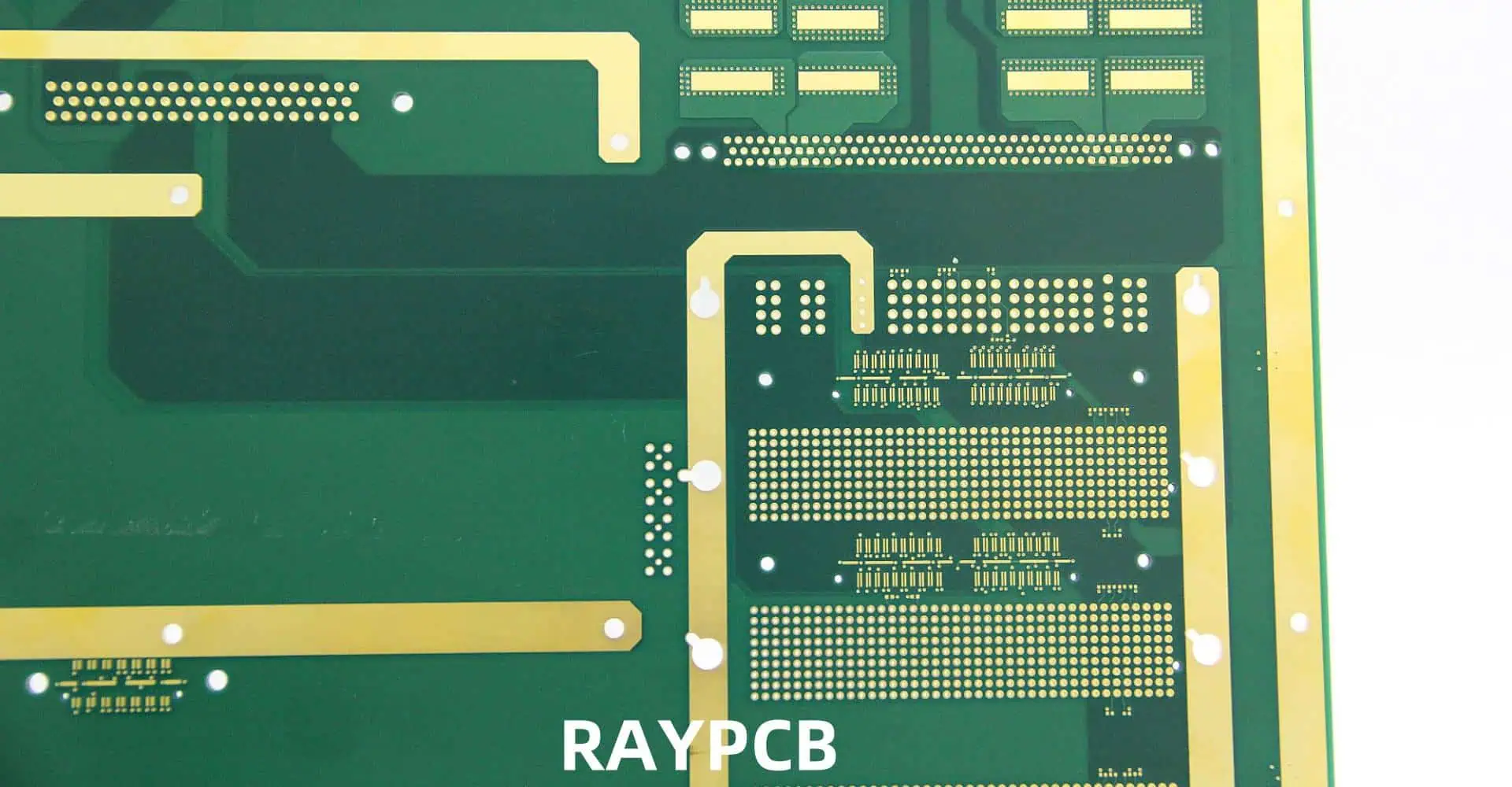
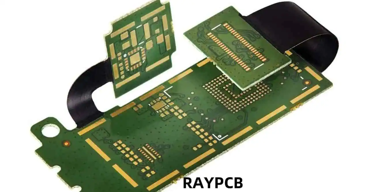
Rigid-flex PCBs are a type of printed circuit board that combines rigid and flexible board technologies. They consist of rigid sections interconnected by flexible sections, allowing for three-dimensional configurations and dynamic flexing applications.

Components of Rigid-Flex PCBs

A typical rigid-flex PCB consists of the following components:

ComponentDescription
Rigid SectionsMade of traditional FR-4 or high-performance laminates
Flexible SectionsComposed of flexible polyimide or similar materials
Copper LayersConduct electrical signals across both rigid and flex sections
CoverlayProtective layer for the flexible sections
AdhesivesBond the various layers together

The Role of Air-Gaps in Rigid-Flex PCBs

Air-gaps play a crucial role in the design and functionality of rigid-flex PCBs. They are intentional spaces left within the PCB structure, typically in the flexible sections or at the transition between rigid and flexible areas.

Purpose of Air-Gaps

The primary purposes of air-gaps in rigid-flex PCBs include:

  1. Enhancing flexibility
  2. Reducing stress on copper traces
  3. Improving thermal management
  4. Facilitating complex bending requirements
  5. Increasing the overall reliability of the PCB

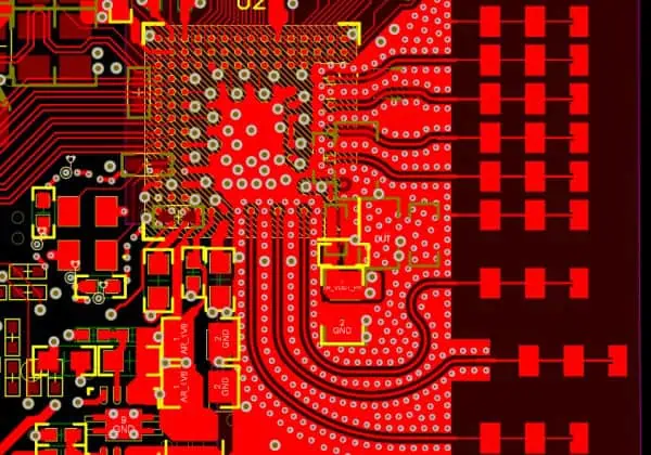
Designing Air-Gaps in Rigid-Flex PCBs

Incorporating air-gaps into rigid-flex PCB designs requires careful consideration and planning. Let’s explore the key aspects of air-gap design.

Types of Air-Gaps

There are several types of air-gaps commonly used in rigid-flex PCBs:

1. Selective Bonding Air-Gaps

These air-gaps are created by selectively applying adhesive in specific areas, leaving other areas unbonded.

2. Cutout Air-Gaps

Cutouts are physical openings in one or more layers of the PCB, creating space for flexing or component clearance.

3. Transition Zone Air-Gaps

These air-gaps are implemented at the junction between rigid and flexible sections to reduce stress and improve reliability.

4. Stress Relief Air-Gaps

Strategically placed air-gaps designed to alleviate mechanical stress in areas prone to repeated bending or flexing.

Design Considerations for Air-Gaps

When incorporating air-gaps into rigid-flex PCB designs, several factors must be considered:

FactorConsideration
LocationPlacement of air-gaps relative to components and traces
SizeDimensions of air-gaps to achieve desired flexibility
ShapeContour of air-gaps to optimize stress distribution
NumberQuantity of air-gaps needed for the application
Layer Stack-upIntegration of air-gaps within the PCB layer structure

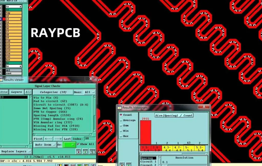
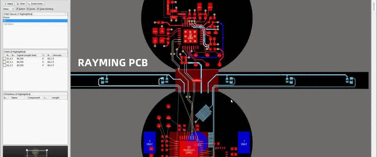
Tools and Software for Air-Gap Design

Designing air-gaps in rigid-flex PCBs requires specialized tools and software. Some popular options include:

  1. Altium Designer
  2. Cadence Allegro
  3. Mentor Graphics Xpedition
  4. Zuken CR-8000

These tools offer features specifically tailored for rigid-flex PCB design, including air-gap modeling and analysis capabilities.

Benefits of Using Air-Gaps in Rigid-Flex PCBs

Incorporating air-gaps into rigid-flex PCB designs offers numerous advantages. Let’s explore some of the key benefits:

1. Enhanced Flexibility

Air-gaps allow for greater flexibility in the bendable sections of the PCB. This increased flexibility enables:

  • Tighter bend radii
  • More complex folding configurations
  • Improved conformability to irregular shapes

2. Reduced Mechanical Stress

By providing space for movement and deformation, air-gaps help reduce mechanical stress on:

  • Copper traces
  • Solder joints
  • Component connections

This stress reduction leads to improved reliability and longer product life.

3. Improved Thermal Management

Air-gaps can act as thermal barriers, helping to:

  • Isolate heat-generating components
  • Reduce heat transfer between sections
  • Improve overall thermal performance

4. Weight Reduction

The inclusion of air-gaps can contribute to overall weight reduction in the PCB assembly, which is crucial for applications such as:

5. Increased Design Flexibility

Air-gaps provide designers with more options for:

  • Component placement
  • Routing traces
  • Accommodating mechanical constraints

Challenges and Considerations in Air-Gap Implementation

rigid-flex-pcb-design

While air-gaps offer numerous benefits, their implementation also comes with challenges that designers must address.

1. Structural Integrity

Balancing flexibility with structural integrity is crucial. Designers must ensure that:

  • The PCB maintains its shape and function
  • Components remain securely attached
  • The overall assembly can withstand expected mechanical stresses

2. Electrical Performance

Air-gaps can affect the electrical characteristics of the PCB. Considerations include:

3. Manufacturing Complexity

Incorporating air-gaps can increase manufacturing complexity, potentially affecting:

4. Cost Implications

The addition of air-gaps may impact the overall cost of the PCB due to:

  • Increased design time
  • More complex manufacturing processes
  • Potential yield issues

5. Reliability and Testing

Ensuring the long-term reliability of rigid-flex PCBs with air-gaps requires:

  • Comprehensive testing protocols
  • Accelerated life testing
  • Consideration of environmental factors (temperature, humidity, etc.)

Best Practices for Air-Gap Design in Rigid-Flex PCBs

To maximize the benefits of air-gaps while minimizing potential issues, designers should follow these best practices:

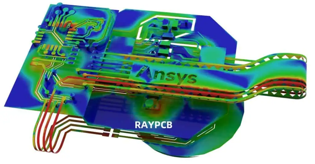
1. Simulate and Analyze

Utilize advanced simulation tools to:

  • Model air-gap behavior under various conditions
  • Analyze stress distribution
  • Optimize air-gap placement and dimensions

2. Consider the Entire System

When designing air-gaps, take into account:

  • Overall product requirements
  • Mechanical constraints
  • Environmental conditions
  • Expected lifecycle

3. Collaborate with Manufacturers

Work closely with PCB fabricators to:

  • Ensure manufacturability of the design
  • Understand process limitations
  • Optimize air-gap implementation for production

4. Implement Gradual Transitions

Design smooth transitions between rigid and flexible sections by:

  • Using stepped layers
  • Implementing transition zones
  • Gradually reducing layer count

5. Conduct Thorough Testing

Develop comprehensive testing protocols that include:

  • Flex testing (static and dynamic)
  • Environmental stress testing
  • Electrical performance verification

Future Trends in Air-Gap Design for Rigid-Flex PCBs

As technology continues to evolve, we can expect to see advancements in air-gap design and implementation for rigid-flex PCBs.

1. Advanced Materials

New materials are being developed that could enhance the performance of air-gaps, including:

  • Novel adhesives with controlled bonding properties
  • High-performance flexible substrates
  • Specialized coatings for improved reliability

2. 3D Printing and Additive Manufacturing

Additive manufacturing techniques may enable:

  • More precise air-gap geometries
  • Custom-designed flexible sections
  • Integration of air-gaps with other PCB features

3. AI and Machine Learning in Design

Artificial intelligence and machine learning algorithms could revolutionize air-gap design by:

  • Optimizing air-gap placement and dimensions
  • Predicting performance under various conditions
  • Automating aspects of the design process

4. Integration with Other Technologies

Air-gap design may be integrated with other emerging technologies, such as:

Conclusion

Air-gaps play a crucial role in the design and performance of rigid-flex PCBs. By providing enhanced flexibility, reducing mechanical stress, and offering design freedom, air-gaps enable the creation of more compact, reliable, and versatile electronic devices. As technology continues to advance, the importance of air-gaps in rigid-flex PCB design is likely to grow, driving innovation in materials, manufacturing processes, and design techniques.

While challenges exist in implementing air-gaps effectively, careful design consideration, advanced simulation tools, and close collaboration with manufacturers can help overcome these obstacles. By following best practices and staying abreast of emerging trends, designers can harness the full potential of air-gaps to create cutting-edge rigid-flex PCB solutions for a wide range of applications.

Frequently Asked Questions (FAQ)

1. What is the primary purpose of using air-gaps in rigid-flex PCBs?

The primary purpose of using air-gaps in rigid-flex PCBs is to enhance flexibility, reduce mechanical stress on copper traces and components, improve thermal management, and increase overall reliability. Air-gaps allow for more complex bending configurations and help the PCB conform to tight spaces or irregular shapes.

2. How do air-gaps affect the electrical performance of a rigid-flex PCB?

Air-gaps can impact the electrical performance of a rigid-flex PCB in several ways. They may affect impedance control, signal integrity, and EMI/EMC performance. Designers need to carefully consider the placement and dimensions of air-gaps to minimize any negative impacts on electrical characteristics while maximizing mechanical benefits.

3. Are there any drawbacks to using air-gaps in rigid-flex PCBs?

While air-gaps offer many benefits, there are some potential drawbacks to consider. These include increased design complexity, potential manufacturing challenges, and possible impacts on structural integrity if not properly implemented. Additionally, the use of air-gaps may increase the overall cost of the PCB due to more complex design and manufacturing processes.

4. How are air-gaps typically created in rigid-flex PCBs?

Air-gaps in rigid-flex PCBs are typically created through several methods:

  1. Selective bonding: applying adhesive only in specific areas
  2. Cutouts: physical openings in one or more layers of the PCB
  3. Transition zones: specially designed areas between rigid and flexible sections
  4. Stress relief patterns: strategically placed openings to alleviate mechanical stress

The specific method used depends on the design requirements and manufacturing capabilities.

5. What future developments can we expect in air-gap technology for rigid-flex PCBs?

Future developments in air-gap technology for rigid-flex PCBs may include:

  • Advanced materials with improved flexibility and bonding properties
  • Integration of 3D printing techniques for more precise air-gap geometries
  • AI-driven optimization of air-gap design and placement
  • Combination of air-gaps with other emerging technologies like embedded components or stretchable electronics

These advancements are likely to expand the capabilities and applications of rigid-flex PCBs in various industries.

SECRETS OF FINE-PITCH PCB ASSEMBLY

Fine-pitch PCB assembly is a critical process in the electronics manufacturing industry, enabling the production of smaller, more complex, and highly efficient electronic devices. As technology advances, the demand for miniaturization and increased functionality in electronic products continues to grow. This article delves into the intricacies of fine-pitch PCB assembly, exploring the challenges, techniques, and best practices that ensure successful outcomes in this demanding field.

What is Fine-Pitch PCB Assembly?

Fine-pitch PCB assembly refers to the process of mounting components with very small lead spacing on printed circuit boards. Typically, fine-pitch components have lead spacings of 0.5 mm or less, pushing the boundaries of traditional PCB assembly techniques.

Evolution of PCB Assembly

To understand the significance of fine-pitch assembly, it’s essential to look at the evolution of PCB assembly:

EraLead PitchTypical Components
1970s-1980s>2.54 mmThrough-hole components
1990s1.27-2.54 mmEarly surface-mount devices (SMDs)
2000s0.5-1.27 mmFine-pitch SMDs
2010s-Present<0.5 mmUltra-fine pitch, BGAs, QFNs

This progression towards finer pitches has been driven by the need for higher component density, improved performance, and reduced device sizes.

Challenges in Fine-Pitch PCB Assembly

1. Component Placement Accuracy

One of the primary challenges in fine-pitch assembly is achieving precise component placement. As lead pitches decrease, the margin for error becomes increasingly small.

Factors Affecting Placement Accuracy:

  • Pick-and-place machine precision
  • Component size and weight
  • PCB warpage
  • Thermal expansion coefficients

2. Solder Paste Deposition

Accurate solder paste deposition is crucial for successful fine-pitch assembly. Challenges include:

  • Controlling solder paste volume
  • Maintaining consistent paste height
  • Avoiding solder bridges between adjacent pads

3. Reflow Process Control

The reflow soldering process becomes more critical with fine-pitch components. Key challenges include:

  • Achieving uniform heating across the PCB
  • Managing thermal profiles for different component types
  • Preventing component shifting during reflow

4. Inspection and Quality Control

Detecting defects in fine-pitch assemblies requires advanced inspection techniques:

  • Limitations of visual inspection
  • Need for automated optical inspection (AOI) systems
  • X-ray inspection for hidden solder joints (e.g., BGAs)

Advanced Techniques for Fine-Pitch PCB Assembly

1. Stencil Design and Printing

Stencil design plays a crucial role in accurate solder paste deposition for fine-pitch components.

Key Considerations in Stencil Design:

FactorDescription
Aperture SizeTypically 80-90% of pad size for fine-pitch components
Stencil ThicknessUsually 3-4 mils (0.076-0.102 mm) for fine-pitch applications
Aperture ShapeCustomized shapes (e.g., home plate) for optimal release
Nano-coatingImproves paste release and reduces bridging

2. Advanced Pick-and-Place Technologies

Modern pick-and-place machines incorporate several technologies to improve accuracy:

  • Vision systems for component alignment
  • Closed-loop feedback for placement verification
  • Multi-nozzle heads for increased throughput
  • Linear motors for smoother, more precise movements

3. Reflow Profiling for Fine-Pitch Components

Developing an optimal reflow profile is critical for fine-pitch assembly success.

Typical Reflow Profile Zones:

  1. Preheat Zone
  2. Soak Zone
  3. Reflow Zone
  4. Cooling Zone

Each zone must be carefully controlled to ensure proper solder joint formation without damaging sensitive components.

4. Nitrogen Reflow Atmosphere

Using a nitrogen atmosphere during reflow can provide several benefits for fine-pitch assembly:

  • Improved wetting and spread of solder
  • Reduced oxidation of solder joints
  • Lower defect rates, especially for lead-free solders

Best Practices for Fine-Pitch PCB Assembly

1. Design for Manufacturability (DFM)

Implementing DFM principles from the outset can significantly improve the success rate of fine-pitch assemblies.

Key DFM Considerations:

  • Adequate spacing between components
  • Proper pad design and solder mask clearances
  • Thermal relief for large ground planes
  • Fiducial marks for accurate component placement

2. Process Control and Monitoring

Maintaining tight control over the assembly process is crucial for consistent results.

Critical Process Parameters to Monitor:

ParameterTypical Range
Solder Paste Temperature20-25ยฐC
Stencil Print Pressure0.18-0.27 kg/cm of squeegee length
Print Speed25-100 mm/s
Reflow Peak Temperature230-250ยฐC (for SAC305 solder)
Cooling Rate2-4ยฐC/s

3. Environmental Control

Maintaining a controlled environment is essential for fine-pitch assembly success.

Environmental Factors to Control:

4. Training and Skill Development

Investing in operator training and skill development is crucial for achieving consistent results in fine-pitch assembly.

Key Training Areas:

  • Proper handling of fine-pitch components
  • Visual inspection techniques
  • Process control and troubleshooting
  • Equipment maintenance and calibration

Advanced Inspection Techniques for Fine-Pitch Assemblies

1. Automated Optical Inspection (AOI)

AOI systems use high-resolution cameras and advanced image processing algorithms to detect defects in fine-pitch assemblies.

Common Defects Detected by AOI:

  • Component misalignment
  • Solder bridges
  • Insufficient solder
  • Missing components

2. X-ray Inspection

X-ray inspection is particularly useful for inspecting hidden solder joints, such as those found in BGA packages.

Advantages of X-ray Inspection:

  • Non-destructive testing
  • Ability to detect voids in solder joints
  • Inspection of multiple board layers

3. In-Circuit Testing (ICT)

ICT provides electrical verification of assembled PCBs, helping to catch defects that may not be visible through optical or X-ray inspection.

ICT Capabilities:

  • Short circuit detection
  • Open circuit detection
  • Component value verification
  • Functional testing of active components

Future Trends in Fine-Pitch PCB Assembly

As technology continues to evolve, several trends are shaping the future of fine-pitch PCB assembly:

1. Further Miniaturization

The drive towards smaller, more powerful devices is pushing lead pitches even lower. Some emerging technologies include:

  • 01005 (0.4 x 0.2 mm) passive components
  • 0.3 mm pitch BGAs
  • Wafer-level chip scale packages (WLCSP)

2. Advanced Materials

New materials are being developed to address the challenges of fine-pitch assembly:

  • Low-temperature solders for heat-sensitive components
  • Novel flux formulations for improved wetting and cleaning
  • High-reliability conformal coatings

3. Artificial Intelligence in Assembly Processes

AI and machine learning are being integrated into various aspects of the assembly process:

  • Predictive maintenance for assembly equipment
  • Real-time process optimization
  • Defect detection and classification in inspection systems

4. Additive Manufacturing Techniques

3D printing and other additive manufacturing techniques are being explored for PCB production, potentially revolutionizing fine-pitch assembly:

  • Printed electronics for flexible circuits
  • Embedded components within PCB substrates
  • Custom package designs for optimal performance

Conclusion

Fine-pitch PCB assembly represents the cutting edge of electronics manufacturing technology. By understanding the challenges, implementing advanced techniques, and following best practices, manufacturers can successfully navigate the complexities of fine-pitch assembly. As technology continues to evolve, staying informed about emerging trends and continuously improving processes will be key to remaining competitive in this demanding field.

Frequently Asked Questions (FAQ)

1. What is considered “fine-pitch” in PCB assembly?

Fine-pitch typically refers to components with lead spacings of 0.5 mm or less. However, the definition can vary depending on the industry and application. Some ultra-fine-pitch components may have lead spacings as small as 0.3 mm or even less.

2. How does fine-pitch assembly differ from standard PCB assembly?

Fine-pitch assembly requires higher precision in all aspects of the process, including stencil printing, component placement, and reflow soldering. It often necessitates specialized equipment, more stringent process controls, and advanced inspection techniques to ensure quality and reliability.

3. What are the most common defects in fine-pitch PCB assembly?

Common defects in fine-pitch assembly include solder bridges (shorts between adjacent pads), insufficient solder (open circuits), component misalignment, and solder balling. These defects can be more difficult to detect and correct compared to those in standard PCB assembly.

4. How can manufacturers improve their fine-pitch assembly capabilities?

Manufacturers can improve their fine-pitch assembly capabilities by investing in advanced equipment, implementing rigorous process controls, providing comprehensive training to operators, and utilizing advanced inspection techniques. Additionally, working closely with PCB designers to ensure design for manufacturability can significantly improve outcomes.

5. What future developments can we expect in fine-pitch PCB assembly?

Future developments in fine-pitch PCB assembly are likely to include further miniaturization of components, advanced materials for improved reliability, integration of artificial intelligence for process optimization, and potentially the adoption of additive manufacturing techniques for PCB production. These developments will enable even more compact and powerful electronic devices in the future.

Which Is Better for PCBs โ€” Potting or Conformal Coating?

When it comes to protecting printed circuit boards (PCBs) from environmental hazards, engineers face a critical decision between two primary protection methods: potting and conformal coating. Both techniques serve the essential purpose of shielding electronic components from moisture, dust, chemicals, vibration, and temperature extremes, but they achieve this protection through fundamentally different approaches. Understanding the distinctions between these methods is crucial for making informed decisions that can significantly impact product performance, longevity, and cost-effectiveness.

YouTube video

Understanding Conformal Coating

Conformal coating represents a thin protective layer, typically ranging from 25 to 250 micrometers in thickness, that is applied directly to the surface of populated PCBs. This protective film conforms to the contours of the circuit board and its components, creating a barrier that maintains access to the board while providing environmental protection.

Types of Conformal Coatings

The conformal coating family includes several material options, each with distinct characteristics. Acrylic coatings offer excellent moisture resistance and optical clarity, making them ideal for applications where visual inspection remains necessary. Silicone coatings provide superior flexibility and temperature resistance, functioning effectively across extreme temperature ranges. Polyurethane coatings deliver robust chemical and abrasion resistance, while parylene coatings offer unparalleled uniformity and penetration into tight spaces.

Application Methods for Conformal Coating

Conformal coatings can be applied through various methods, including spray coating, dip coating, brush application, and selective coating systems. Spray coating provides excellent control and is suitable for high-volume production, while dip coating ensures comprehensive coverage for complex geometries. Selective coating systems offer precision application, allowing specific areas to remain uncoated for connections or heat dissipation.

Understanding Potting Compounds

Potting involves completely encapsulating electronic assemblies in a solid or gel-like compound, creating a protective shell around the entire circuit. This method provides maximum environmental protection by completely sealing components from external influences. Potting compounds typically range from flexible gels to rigid thermoset materials, offering varying degrees of protection and accessibility.

Types of Potting Materials

Potting materials include epoxy resins, which provide excellent mechanical strength and chemical resistance; silicone compounds, offering flexibility and temperature stability; and polyurethane materials, delivering good mechanical properties with moderate flexibility. Each material type brings specific advantages depending on the application requirements and environmental conditions.

Potting Application Process

The potting process involves placing the PCB assembly into a housing or mold, then dispensing the potting compound to completely surround the components. The material is then cured through heat, chemical reaction, or UV exposure, depending on the compound type. This process requires careful consideration of air bubble elimination, proper mixing ratios, and curing parameters to achieve optimal results.

Comparative Analysis: Protection Levels

When evaluating protection effectiveness, potting generally provides superior environmental protection due to its complete encapsulation approach. Potted assemblies offer exceptional resistance to moisture ingress, dust contamination, and chemical exposure. The thick barrier created by potting compounds also provides excellent vibration damping and shock protection, making this method ideal for harsh industrial or military applications.

Conformal coating, while providing good environmental protection, offers a lighter level of defense. The thin coating effectively prevents moisture and contaminant contact with circuit elements but may not provide adequate protection in extremely harsh environments. However, conformal coatings excel in applications where some level of environmental protection is needed without completely isolating the circuit from its surroundings.

Maintenance and Rework Considerations

One of the most significant differences between these protection methods lies in their impact on maintenance and rework capabilities. Conformal coatings can often be removed through solvent dissolution, mechanical scraping, or thermal methods, allowing for component replacement and circuit modifications. This reversibility makes conformal coating attractive for applications where future modifications or repairs are anticipated.

Potting compounds, particularly rigid formulations, create permanent encapsulation that makes component access extremely difficult or impossible. While some soft potting gels can be mechanically removed, the process is often time-consuming and may damage delicate components. This irreversibility must be carefully considered during the design phase, as it essentially makes the assembly disposable in many cases.

Cost Considerations and Economic Impact

From an economic perspective, conformal coating typically requires lower initial material costs and simpler application equipment. The thin film application uses minimal material, and the coating process can often be integrated into existing production lines with moderate equipment investment. Labor costs remain relatively low, and the reversible nature of most coatings provides long-term value through repairability.

Potting generally involves higher material costs due to the volume of compound required to fill the enclosure completely. Additionally, potting often necessitates custom housings or molds, adding tooling costs to the overall project expense. The specialized dispensing equipment and curing systems required for potting also represent significant capital investments, particularly for automated production systems.

Performance in Specific Applications

The choice between potting and conformal coating often depends heavily on the specific application environment and requirements. In aerospace and military applications, where maximum protection is paramount and cost is secondary, potting frequently provides the necessary level of environmental protection. The complete encapsulation protects against extreme temperature cycling, high humidity, salt spray, and mechanical shock that aircraft and military equipment regularly encounter.

For consumer electronics and commercial applications, conformal coating often represents the optimal balance between protection and practicality. Products like smartphones, computers, and home appliances benefit from the moisture and dust protection that conformal coating provides while maintaining the ability for service and repair. The thinner profile also helps maintain compact product designs where space is at a premium.

Industrial applications present varied requirements that may favor either approach. Process control systems in chemical plants might require the complete isolation that potting provides, while automation equipment that requires regular maintenance might benefit more from the accessibility that conformal coating allows.

Making the Right Choice

The decision between potting and conformal coating should be based on a comprehensive evaluation of environmental requirements, maintenance needs, cost constraints, and performance expectations. Applications requiring maximum environmental protection, where maintenance is minimal and cost is not the primary concern, often benefit from potting solutions. Conversely, applications needing moderate protection with maintained accessibility for service and repair typically favor conformal coating approaches.

The optimal choice also depends on production volume, available manufacturing capabilities, and long-term product strategy. High-volume production might favor conformal coating due to its streamlined application process, while low-volume, high-reliability applications might justify the additional complexity and cost of potting.

Both potting and conformal coating represent effective protection strategies, each with distinct advantages and limitations. The key to success lies in carefully matching the protection method to the specific application requirements, ensuring that the chosen approach delivers the necessary performance while maintaining economic viability and practical functionality throughout the product lifecycle.

PCB Manufacturers for Hobbyists & College Students: Your Complete Guide to Affordable Circuit Board Production

multilayer pcb manufacturers

Creating custom printed circuit boards (PCBs) has never been more accessible for hobbyists and college students. With the rise of affordable online PCB manufacturing services, anyone can transform their circuit designs from breadboard prototypes into professional-looking boards. This comprehensive guide explores the best PCB manufacturers that cater specifically to budget-conscious makers, students, and electronics enthusiasts.

Why Choose Professional PCB Manufacturing Over DIY Methods?

While it’s possible to create PCBs at home using etching methods, professional manufacturing offers significant advantages. Professional PCBs provide superior reliability, cleaner traces, and the ability to create complex multi-layer designs that would be impossible to achieve at home. Additionally, modern PCB manufacturers offer competitive pricing that often makes professional production more cost-effective than DIY methods when factoring in time, materials, and success rates.

Professional PCBs also support advanced features like soldermask, silkscreen labeling, plated through-holes, and surface mount component compatibility. These features are essential for creating projects that look professional and function reliably over time.

Top PCB Manufacturers for Budget-Conscious Projects

Rogers AD255C PCB

JLCPCB: The Student Favorite

JLCPCB has emerged as the go-to choice for hobbyists and students worldwide. Their promotional pricing of $2 for five 100mm x 100mm PCBs makes it incredibly affordable to experiment with designs. The company offers excellent quality control, fast turnaround times, and ships globally with reasonable shipping costs.

What makes JLCPCB particularly attractive is their integrated ecosystem. Beyond PCB manufacturing, they offer component sourcing and assembly services, allowing students to order both the board and components in one place. Their online quotation system is transparent, showing exact costs upfront without hidden fees.

PCBWay: Quality and Community Focus

PCBWay has built a strong reputation among the maker community by consistently delivering high-quality boards with excellent customer service. They offer competitive pricing for small quantities and frequently run promotions specifically targeting students and hobbyists.

The company stands out for its comprehensive manufacturing capabilities, including flexible PCBs, aluminum boards, and advanced multi-layer designs. Their online design rule check helps catch potential issues before manufacturing, reducing the likelihood of receiving unusable boards.

OSH Park: Made in USA Option

For those preferring domestic manufacturing, OSH Park offers PCB production within the United States. While slightly more expensive than overseas options, they provide faster shipping to North American customers and excellent quality control. Their distinctive purple soldermask has become iconic in the maker community.

OSH Park uses a unique pricing model based on square inches rather than board count, which can be economical for very small designs. They also offer a shared projects gallery where users can order copies of open-source designs created by other makers.

Understanding PCB Specifications for Student Projects

Layer Count Considerations

Most hobbyist projects can be accomplished with single or double-layer PCBs, which are the most economical options. Single-layer boards work well for simple circuits with minimal complexity, while double-layer boards provide more routing flexibility for projects with multiple components or complex connections.

Four-layer boards become necessary for high-speed digital circuits, RF applications, or designs requiring dedicated power and ground planes. While more expensive, four-layer boards often provide better signal integrity and reduced electromagnetic interference.

Size Limitations and Cost Optimization

Understanding size limitations helps optimize costs. Most manufacturers offer attractive pricing for boards under 100mm x 100mm, with costs increasing significantly for larger sizes. Smart designers learn to partition large projects into smaller boards that can be connected together, maintaining low costs while achieving complex functionality.

Consider the aspect ratio of your design as well. Extremely long, narrow boards may incur additional charges due to manufacturing constraints and material waste during the panelization process.

Design Software Options for Students

Free and Open Source Solutions

KiCad has become the standard free PCB design software for hobbyists and students. It offers professional-grade features including schematic capture, PCB layout, 3D visualization, and extensive component libraries. The software receives regular updates and has excellent community support through forums and tutorials.

FreeCAD and other open-source tools can complement KiCad for mechanical design integration, allowing students to create complete product designs that consider both electronic and mechanical requirements.

Educational Licenses for Professional Tools

Many professional PCB design tools offer free educational licenses for students. Altium Designer, considered the industry standard, provides student licenses that include full functionality. Similarly, Autodesk EAGLE offers educational versions that remove commercial use restrictions while providing professional capabilities.

These tools often integrate directly with major PCB manufacturers, streamlining the process from design to production. Learning professional tools during college can provide valuable skills for future career opportunities.

Online Design Tools

Browser-based design tools like EasyEDA have gained popularity for their convenience and integrated manufacturing workflows. These tools require no software installation and often connect directly to PCB manufacturing services, simplifying the ordering process for beginners.

While online tools may lack some advanced features of desktop software, they provide an excellent starting point for students new to PCB design and can handle the majority of hobbyist projects effectively.

Cost Management Strategies for Student Projects

Group Orders and Bulk Purchasing

One of the most effective cost reduction strategies involves organizing group orders with classmates or local maker groups. Since most manufacturers have minimum order quantities that exceed individual needs, splitting orders among multiple people reduces per-board costs significantly.

Many manufacturers offer volume discounts that kick in at relatively low quantities, making group purchases financially attractive. Coordinate with study groups, engineering clubs, or local hackerspaces to identify others working on projects.

Timing Orders for Maximum Savings

PCB manufacturers frequently offer promotional pricing, especially during slower business periods. Following manufacturers on social media or subscribing to newsletters can provide advance notice of sales and special offers.

Consider timing orders to avoid rush charges. Most manufacturers offer standard turnaround times of 5-10 business days at base pricing, with expedited options available for additional fees. Planning ahead eliminates the need for expensive rush orders.

Design Optimization for Cost Reduction

Simple design choices can significantly impact manufacturing costs. Minimizing layer count, avoiding exotic materials, and staying within standard size limitations keeps costs low. Using standard via sizes and avoiding minimum spacing requirements prevents additional charges for advanced manufacturing processes.

Consider the total cost of ownership beyond just PCB manufacturing. Designs that accommodate readily available components and standard assembly processes reduce overall project costs and complexity.

Quality Assurance and Testing

Understanding Manufacturing Tolerances

Professional PCB manufacturers maintain strict quality control standards, but understanding normal manufacturing tolerances helps set realistic expectations. Trace widths, hole sizes, and component placement all have acceptable variation ranges that rarely affect functionality but may be noticeable upon close inspection.

Most manufacturers provide detailed specifications for their standard processes, allowing designers to understand what level of precision to expect. This information helps in creating designs that work reliably within normal manufacturing variations.

Inspection and Testing Procedures

Reputable manufacturers perform electrical testing on every board to verify continuity and identify short circuits. However, functional testing of the complete circuit remains the designer’s responsibility. Plan for basic testing procedures to verify your boards work as intended before integrating them into larger projects.

Consider designing test points into your PCBs to facilitate troubleshooting and verification. These small additions can save significant time during the debugging process and help identify whether issues stem from design errors or manufacturing defects.

Building Relationships with Manufacturers

Communication and Support

Establishing good relationships with PCB manufacturer support teams can provide valuable assistance throughout your educational journey. Many manufacturers offer technical support to help resolve design issues and manufacturing questions.

Don’t hesitate to reach out with questions about capabilities, specifications, or design optimization. Most manufacturers prefer to address potential issues before production rather than dealing with problematic orders after the fact.

Long-term Considerations

As students transition into professional careers, the relationships and knowledge gained through educational projects can prove valuable. Understanding manufacturing processes, cost structures, and quality expectations provides a solid foundation for future professional work in electronics design and development.

Consider how your choice of manufacturers and design practices during school might influence your future career path. Experience with industry-standard tools and processes can provide competitive advantages in the job market.

Professional PCB manufacturing has revolutionized electronics education and hobbyist projects by making high-quality circuit boards accessible and affordable. By understanding the options available, optimizing designs for cost-effectiveness, and building good relationships with manufacturers, students and hobbyists can create impressive projects that demonstrate both technical competence and professional presentation. The key lies in balancing cost, quality, and learning objectives to maximize the educational value of each project while staying within budget constraints.

Reducing Design Costs in Printed Circuit Boards

Printed Circuit Board (PCB) design represents a significant portion of electronic product development costs, often accounting for 15-30% of total manufacturing expenses. As global competition intensifies and profit margins shrink, engineers and product managers must find innovative ways to optimize PCB design costs without compromising functionality or reliability. This comprehensive guide explores proven strategies to reduce PCB design expenses while maintaining quality standards.

YouTube video

Understanding PCB Cost Drivers

Material and Manufacturing Factors

The foundation of cost-effective PCB design begins with understanding what drives expenses. Raw materials typically constitute 40-60% of total PCB costs, with copper being the most significant contributor. The thickness of copper layers, number of layers, and substrate material directly impact pricing. Standard FR-4 substrates offer the best cost-to-performance ratio for most applications, while exotic materials like Rogers or Teflon should be reserved for high-frequency applications where they provide measurable benefits.

Manufacturing complexity adds substantial costs through specialized processes. Via types, drill sizes, trace widths, and spacing requirements all influence manufacturing difficulty and yield rates. Each additional manufacturing step introduces potential failure points and increases labor costs, making simplicity a valuable design principle.

Design Complexity Impact

Complex designs require more engineering hours, extended testing phases, and often multiple prototype iterations. Features like blind vias, buried vias, and microvias can increase costs by 200-500% compared to standard through-hole vias. Similarly, tight spacing requirements may necessitate advanced manufacturing processes that command premium pricing.

Strategic Design Approaches for Cost Reduction

Optimize Layer Count and Stack-up

One of the most impactful cost reduction strategies involves minimizing layer count while maintaining signal integrity. Each additional layer increases material costs and manufacturing complexity exponentially rather than linearly. A four-layer board typically costs 40-60% more than a two-layer equivalent, while an eight-layer board can cost 300-400% more.

Careful component placement and routing optimization often enables designers to achieve the same functionality with fewer layers. Mixed-signal designs benefit from proper ground plane management, which can eliminate the need for additional shielding layers. Power distribution networks can be optimized through strategic decoupling capacitor placement rather than dedicated power layers.

Standardize Design Rules and Specifications

Establishing and adhering to standard design rules across projects reduces manufacturing costs through improved yields and simplified processes. Standard via sizes, trace widths, and spacing requirements enable manufacturers to use proven processes and tooling, reducing setup costs and minimizing defects.

Creating design rule libraries that align with preferred manufacturers’ capabilities ensures compatibility and cost-effectiveness. These libraries should include standard drill sizes, minimum trace widths, and preferred component footprints that balance performance requirements with manufacturing constraints.

Component Selection and Placement Strategies

YouTube video

Choose Standard Components

Component selection significantly impacts both direct costs and manufacturing efficiency. Standard package sizes like 0603, 0805, and 1206 for passive components offer the best balance of cost, availability, and assembly reliability. Avoiding exotic packages reduces component costs and simplifies assembly processes.

Standardizing on common component values reduces inventory complexity and enables volume purchasing benefits. Using preferred manufacturer parts lists ensures long-term availability and competitive pricing. This approach also simplifies supply chain management and reduces the risk of component obsolescence.

Optimize Component Placement

Strategic component placement reduces PCB area requirements and simplifies routing, directly impacting costs. Grouping related components minimizes trace lengths and reduces electromagnetic interference, potentially eliminating the need for additional shielding or filtering components.

High-power components should be positioned to take advantage of natural heat dissipation paths, reducing the need for expensive thermal management solutions. Connector placement affects enclosure design costs and assembly complexity, making early coordination between PCB and mechanical designs essential.

Manufacturing and Assembly Considerations

Design for Manufacturability (DFM)

Implementing DFM principles from the project’s inception prevents costly redesigns and manufacturing delays. Standard drill sizes reduce tooling costs and improve yield rates. Manufacturers typically offer better pricing for designs using their preferred drill sizes and processes.

Panelization strategies can significantly reduce per-unit costs for small PCBs. Designing boards to fit efficiently within standard panel sizes maximizes material utilization and reduces waste. Proper panelization also improves assembly efficiency and reduces handling costs.

Assembly Optimization

Component orientation standardization reduces assembly time and potential errors. Aligning all polarized components in the same direction simplifies pick-and-place programming and reduces assembly errors. This approach also improves visual inspection efficiency and reduces testing time.

Test point accessibility and placement affect manufacturing test costs significantly. Well-designed test strategies reduce test time and improve fault detection rates, minimizing rework costs. In-circuit test (ICT) strategies should be considered during initial design phases rather than added later.

Advanced Cost Reduction Techniques

Multi-project Sharing

Combining multiple small projects into single manufacturing runs leverages economies of scale effectively. This approach works particularly well for companies with multiple product lines or when collaborating with partners on complementary products.

Shared tooling costs and setup fees can reduce per-unit expenses by 30-50% for small to medium volume runs. Careful coordination of project timelines enables this strategy without impacting individual project schedules.

Alternative Materials and Processes

Exploring alternative substrate materials can yield significant cost savings for appropriate applications. CEM-1 and CEM-3 substrates offer cost advantages over FR-4 for simple, low-frequency applications. However, these alternatives require careful evaluation of electrical and mechanical properties.

Flexible-rigid PCB designs can eliminate connectors and cables in some applications, reducing both material costs and assembly complexity. While the PCB itself may be more expensive, total system costs often decrease through simplified assembly and improved reliability.

Long-term Cost Management Strategies

Supplier Relationships and Volume Planning

Developing strong relationships with PCB manufacturers enables better pricing negotiations and priority treatment during capacity constraints. Long-term partnerships often result in preferential pricing and access to advanced manufacturing capabilities.

Volume forecasting accuracy directly impacts pricing structures. Manufacturers offer significant discounts for committed volumes, making accurate demand planning essential for cost optimization. Flexible manufacturing agreements can balance cost savings with inventory risk management.

Design Reuse and Standardization

Creating reusable design blocks and reference designs accelerates development while reducing engineering costs. Standard power supply circuits, communication interfaces, and protection circuits can be validated once and reused across multiple projects.

Platform-based design approaches enable cost amortization across product families. Common base designs with application-specific modifications reduce development time and leverage previous validation efforts.

Measuring and Monitoring Cost Effectiveness

Implementing cost tracking systems throughout the design process enables continuous improvement. Regular cost analysis helps identify trends and opportunities for further optimization. Key metrics include cost per square inch, component costs as percentage of total, and manufacturing yield rates.

Design review processes should include cost implications alongside technical considerations. Early identification of cost drivers enables proactive optimization rather than reactive cost reduction efforts.

Conclusion

Reducing PCB design costs requires a systematic approach that balances technical requirements with economic realities. Success comes from understanding cost drivers, implementing proven design strategies, and maintaining focus on manufacturability throughout the design process. The strategies outlined in this guide can typically reduce PCB costs by 20-40% while maintaining or improving product performance and reliability.

Cost optimization should be viewed as an ongoing process rather than a one-time effort. Regular review and refinement of design practices, supplier relationships, and manufacturing strategies ensures continued competitiveness in evolving markets. The investment in cost reduction strategies pays dividends through improved profit margins and market positioning.

Improving PCB Quality Through Even Copper Distribution

The quality and reliability of printed circuit boards (PCBs) fundamentally depend on the uniformity of copper distribution across their surface. Even copper distribution is not merely an aesthetic consideration but a critical factor that directly impacts electrical performance, thermal management, mechanical integrity, and manufacturing yield. Understanding and implementing strategies for achieving uniform copper distribution represents one of the most significant opportunities for PCB designers and manufacturers to enhance product quality and reduce field failures.

YouTube video

Understanding Copper Distribution Fundamentals

Copper distribution refers to how copper traces, planes, and features are arranged across a PCB’s surface area. In an ideally designed board, copper should be distributed as evenly as possible to maintain consistent electrical and thermal properties throughout the substrate. Uneven copper distribution creates localized areas of high and low copper density, leading to a cascade of quality issues that can compromise the entire circuit board’s functionality.

The physics behind copper distribution effects are rooted in the PCB manufacturing process itself. During fabrication, the board undergoes various thermal cycles including lamination, soldering, and reflow processes. Areas with dense copper concentrations expand and contract differently than areas with sparse copper coverage due to the significant difference in thermal expansion coefficients between copper and the substrate material. This differential expansion creates internal stresses that can manifest as warpage, delamination, or even copper trace cracking over time.

Manufacturing Process Implications

The impact of copper distribution becomes apparent during the etching process, where uneven copper densities can lead to inconsistent etch rates across the board. Areas with high copper density may experience over-etching or under-etching compared to sparse areas, resulting in trace width variations that directly affect impedance control and signal integrity. This manufacturing variability translates to increased scrap rates and reduced yields, making even copper distribution a critical economic consideration for manufacturers.

Plating processes are similarly affected by copper distribution uniformity. During electroplating, current density varies inversely with copper coverage, meaning areas with less existing copper receive more plating current and thus thicker copper deposits. This creates a snowball effect where uneven distribution becomes more pronounced through successive manufacturing steps. The result is inconsistent via fill, varying trace thickness, and unpredictable electrical characteristics across the finished board.

Electrical Performance Considerations

From an electrical standpoint, uneven copper distribution directly impacts signal integrity and power delivery performance. Impedance control, which is crucial for high-speed digital circuits, becomes significantly more challenging when copper distribution varies across the board. Transmission lines require consistent cross-sectional geometry to maintain target impedance values, but variations in copper thickness and spacing due to uneven distribution create impedance discontinuities that can cause signal reflections, increased EMI, and timing errors.

Power distribution networks (PDN) are particularly sensitive to copper distribution uniformity. Modern electronic devices demand clean, stable power delivery with minimal voltage ripple and noise. Uneven copper distribution in power planes creates areas of high and low impedance, leading to uneven current distribution and voltage drops that can affect circuit performance. Critical analog circuits may experience increased noise, while digital circuits might suffer from timing variations and increased jitter.

Ground planes, which serve as return paths for high-frequency signals, must maintain consistent impedance characteristics to ensure proper signal return currents. Variations in copper distribution create impedance variations in the ground plane, forcing return currents to take suboptimal paths that can increase crosstalk between adjacent signals and degrade overall system performance.

Thermal Management Benefits

Thermal management represents another critical aspect where even copper distribution provides substantial benefits. Copper’s excellent thermal conductivity makes it an effective heat spreader, but only when distributed uniformly across the board. Concentrated copper areas create thermal hotspots that can stress components and reduce their operational lifetime, while areas with insufficient copper coverage may not adequately dissipate heat generated by nearby components.

Even copper distribution enables more predictable thermal modeling and analysis during the design phase. Thermal simulation tools can more accurately predict temperature distributions when copper coverage is uniform, allowing designers to make informed decisions about component placement and thermal management strategies. This predictability reduces the need for extensive prototyping and testing, accelerating time-to-market while improving product reliability.

The thermal expansion benefits of even copper distribution cannot be overstated. When copper is distributed evenly, the entire PCB expands and contracts more uniformly during thermal cycling, reducing internal stresses that can lead to solder joint failures, component cracking, or substrate delamination. This is particularly important for products that experience wide temperature variations during operation or storage.

Design Strategies for Achieving Uniform Distribution

Achieving even copper distribution requires deliberate design strategies implemented from the earliest stages of PCB layout. Copper balancing techniques involve adding copper fills, dummy features, or adjusting trace routing to achieve more uniform coverage across each layer. Modern PCB design software includes copper balancing tools that can automatically calculate and adjust copper distribution, but designers must understand the underlying principles to use these tools effectively.

Strategic copper fill placement represents one of the most effective techniques for improving distribution uniformity. Rather than simply flooding empty areas with solid copper, designers should implement hatched or grid-pattern fills that provide more controlled copper coverage. These patterns can be optimized to achieve target copper percentages while maintaining appropriate clearances from active circuits.

Via stitching and thermal vias serve dual purposes in copper distribution optimization. Beyond their primary function of providing interlayer connections, strategically placed vias can help balance copper distribution while improving thermal performance. Dense via patterns in low-copper areas can increase local copper content while providing thermal pathways between layers.

Layer stackup design plays a crucial role in achieving even copper distribution. Alternating signal and plane layers with complementary copper patterns can help balance overall distribution while maintaining good electrical performance. Designers should consider the cumulative effect of all layers when evaluating copper distribution rather than optimizing individual layers in isolation.

Advanced Copper Management Techniques

Modern PCB design increasingly relies on advanced copper management techniques that go beyond traditional copper fills. Copper thieving involves adding non-functional copper features specifically to balance copper distribution without affecting circuit operation. These features can be strategically sized and placed to achieve target copper percentages while maintaining isolation from active circuits.

Hatched copper fills offer advantages over solid fills for copper distribution applications. The hatched pattern provides more controlled copper coverage and can be adjusted to achieve precise copper percentages. Additionally, hatched fills reduce the risk of creating large copper areas that might cause manufacturing issues or electromagnetic interference.

Cross-hatching patterns can be optimized for specific applications, with factors such as line width, spacing, and orientation affecting both copper coverage and electrical performance. Advanced design rules can automatically generate optimized cross-hatch patterns based on local copper density requirements and electrical constraints.

Quality Assurance and Testing

Implementing even copper distribution requires robust quality assurance processes to verify that design intentions translate to manufactured reality. Copper distribution analysis should be integrated into the design review process, with specific criteria for acceptable copper percentage variations across the board area. Statistical process control techniques can track copper distribution consistency across production lots, identifying trends that might indicate process drift or equipment issues.

Visual inspection techniques can identify gross copper distribution problems, but quantitative measurement requires specialized equipment. Automated optical inspection (AOI) systems can measure copper coverage percentages across defined areas, providing objective data for quality assessment. X-ray inspection can reveal copper distribution in inner layers that are not visible through conventional optical inspection.

Electrical testing can validate the functional impact of copper distribution decisions. Impedance testing should verify that copper distribution variations do not create unacceptable impedance variations. Power delivery network analysis can confirm that even copper distribution provides the intended benefits for power system performance.

Economic and Manufacturing Considerations

The business case for even copper distribution extends beyond technical performance to encompass manufacturing efficiency and cost reduction. Improved manufacturing yields result from more predictable etching and plating processes, reducing scrap and rework costs. Consistent electrical performance reduces the need for expensive testing and sorting operations, while improved reliability reduces warranty costs and field failures.

Long-term reliability benefits translate to competitive advantages in markets where product longevity is valued. Applications such as automotive electronics, medical devices, and industrial controls particularly benefit from the enhanced reliability that even copper distribution provides. The investment in design time and analysis tools required to achieve even copper distribution typically pays for itself through reduced manufacturing costs and improved customer satisfaction.

Even copper distribution represents a fundamental aspect of PCB quality that impacts every aspect of circuit board performance from manufacturing through end-of-life. By understanding the underlying principles and implementing appropriate design strategies, PCB designers and manufacturers can significantly improve product quality, reliability, and manufacturing efficiency. The investment in achieving uniform copper distribution pays dividends throughout the product lifecycle, making it an essential consideration for any quality-focused PCB development program.

How to Avoid DFM Issues: A Comprehensive Guide to Design for Manufacturing

Design for Manufacturing (DFM) is a critical engineering methodology that focuses on designing products in a way that makes them easier, faster, and more cost-effective to manufacture. DFM issues can lead to production delays, increased costs, quality problems, and even complete product redesigns. Understanding how to avoid these pitfalls is essential for any product development team aiming to bring successful products to market.

Understanding DFM Fundamentals

DFM issues typically arise when designers create products without considering the constraints and capabilities of the manufacturing processes that will be used to produce them. These problems manifest in various forms: parts that are impossible to manufacture with available equipment, designs that require excessive machining time, assemblies that are difficult to put together, or products that suffer from poor quality due to manufacturing limitations.

The core principle of effective DFM is to integrate manufacturing considerations into the design process from the earliest stages, rather than treating manufacturing as an afterthought. This proactive approach prevents costly redesigns and ensures that products can be manufactured efficiently at scale.

YouTube video

Early Collaboration and Communication

One of the most effective ways to avoid DFM issues is establishing strong communication channels between design teams and manufacturing personnel from the project’s inception. Designers should regularly consult with manufacturing engineers, machinists, and production supervisors to understand the capabilities and limitations of available manufacturing processes.

Regular design reviews that include manufacturing stakeholders help identify potential issues before they become costly problems. These reviews should cover material selection, dimensional tolerances, surface finish requirements, and assembly processes. Manufacturing teams can provide valuable insights about which design features are easy to produce and which might cause difficulties or increase costs.

Creating cross-functional teams that include both design and manufacturing representatives ensures that manufacturing considerations are embedded throughout the design process. This collaborative approach helps designers understand the practical implications of their design decisions and enables manufacturing teams to prepare for production requirements early in the development cycle.

Material Selection and Properties

Choosing appropriate materials is fundamental to avoiding DFM issues. Materials must not only meet functional requirements but also be compatible with intended manufacturing processes. For example, selecting a material that cannot withstand the temperatures required for a specific molding process will create immediate manufacturing problems.

Designers should consider material availability, cost, and supply chain reliability when making selections. Specifying exotic or hard-to-source materials can lead to production delays and increased costs. Similarly, materials with inconsistent properties or quality can cause manufacturing variability and quality issues.

Understanding how materials behave during manufacturing processes is crucial. Some materials may warp during heat treatment, others might be prone to cracking during machining, and certain plastics may have unpredictable shrinkage rates during molding. Working closely with material suppliers and conducting material testing early in the design process helps avoid these issues.

Tolerance and Dimensional Considerations

Overly tight tolerances are among the most common DFM issues. While precision is often important for product function, specifying tolerances that are tighter than necessary significantly increases manufacturing costs and complexity. Each manufacturing process has inherent capabilities and limitations regarding the tolerances it can achieve economically.

Designers should understand the natural tolerances of different manufacturing processes and design accordingly. For instance, injection molding typically achieves different tolerances than CNC machining, and sand casting has different capabilities than investment casting. Specifying tolerances that align with process capabilities reduces costs and improves manufacturability.

Tolerance stack-up analysis is essential for complex assemblies. Understanding how individual part tolerances combine to affect overall assembly dimensions helps designers specify appropriate tolerances for each component. This analysis often reveals that some tight tolerances are unnecessary and can be relaxed without affecting product function.

Process-Specific Design Guidelines

Each manufacturing process has specific design guidelines that, when followed, significantly reduce the likelihood of DFM issues. For injection molding, this includes considerations like wall thickness uniformity, draft angles, undercuts, and gate placement. Parts designed without adequate draft angles may be difficult to remove from molds, while non-uniform wall thickness can cause warping and sink marks.

For machined parts, designers should consider tool access, setup requirements, and material removal efficiency. Features that require special tooling or complex setups increase manufacturing costs and time. Designing parts that can be machined with standard tools and minimal setups improves manufacturability and reduces costs.

Sheet metal parts require attention to bend radii, hole spacing, and material utilization. Bends that are too tight for the material thickness can cause cracking, while poor hole placement might interfere with standard tooling. Designing parts that make efficient use of standard sheet sizes reduces material waste and costs.

Assembly and Fastening Strategies

Complex assemblies often present significant DFM challenges. Parts that are difficult to access during assembly, require special tools, or must be assembled in a specific sequence can create production bottlenecks and quality issues. Designing for assembly (DFA) principles should be integrated with DFM considerations to create products that are both manufacturable and assemblable.

Reducing the number of parts in an assembly often improves both manufacturability and assembly efficiency. Part consolidation through design optimization or alternative manufacturing processes can eliminate assembly steps and reduce inventory complexity. However, this must be balanced against the manufacturability of individual parts.

Fastening methods should be chosen based on assembly requirements, accessibility, and cost considerations. Self-tapping screws might be appropriate for some applications but could cause assembly difficulties in others. Similarly, press-fits and snap-fits can eliminate fasteners but require precise manufacturing tolerances.

Quality and Inspection Considerations

Designing parts that are easy to inspect and test helps avoid quality-related DFM issues. Features that are difficult to measure or inspect can lead to quality problems that are discovered late in the production process. Providing adequate access for measurement tools and inspection equipment should be considered during the design phase.

Statistical process control (SPC) requirements should influence design decisions. Parts designed with features that are inherently stable and controllable during manufacturing will have fewer quality issues than parts that push manufacturing processes to their limits. Understanding process capability and designing within these limits improves overall product quality.

Critical dimensions and features should be easily accessible for inspection. Hidden or hard-to-reach features may not be properly inspected, leading to quality escapes. Designing parts with inspection access in mind helps ensure consistent quality throughout production.

Cost Optimization Strategies

DFM is closely tied to cost optimization. Many DFM issues directly translate to increased manufacturing costs. Understanding the cost drivers in different manufacturing processes helps designers make informed decisions that balance functionality with manufacturability and cost.

Standard features and dimensions typically cost less to produce than custom requirements. Using standard hole sizes, thread pitches, and material thicknesses where possible reduces tooling costs and improves manufacturability. Similarly, designing parts that can be produced with standard manufacturing equipment eliminates the need for special tooling or processes.

Production volume significantly impacts manufacturing process selection and design requirements. Low-volume products might be best suited for machining or 3D printing, while high-volume products benefit from processes like injection molding or stamping. Designing for the appropriate production volume ensures optimal cost and manufacturability.

Continuous Improvement and Learning

Avoiding DFM issues is an ongoing process that requires continuous learning and improvement. Establishing feedback loops between manufacturing and design teams helps identify recurring issues and develop solutions. Post-production reviews that analyze manufacturing challenges provide valuable insights for future designs.

Staying current with manufacturing technology and capabilities is essential. New processes, materials, and equipment regularly become available, offering new possibilities for design optimization. Regular training and industry engagement help design teams stay aware of evolving manufacturing capabilities.

Building design guidelines and standards based on past experience helps institutionalize DFM knowledge within organizations. These guidelines should be regularly updated based on new learnings and shared across design teams to prevent repeated mistakes.

Conclusion

Avoiding DFM issues requires a systematic approach that integrates manufacturing considerations throughout the design process. Success depends on early collaboration between design and manufacturing teams, understanding process capabilities and limitations, and making informed decisions about materials, tolerances, and design features. By following these principles and maintaining a focus on continuous improvement, organizations can significantly reduce DFM issues and create products that are both functional and manufacturable. The investment in proper DFM practices pays dividends through reduced costs, shorter development cycles, and improved product quality.

How to Select High-Frequency PCB Materials

The selection of appropriate materials for high-frequency printed circuit boards (PCBs) is a critical decision that directly impacts signal integrity, performance, and reliability in modern electronic systems. As operating frequencies continue to increase in applications ranging from 5G communications to radar systems, understanding the nuances of high-frequency PCB material selection becomes increasingly important for engineers and designers.

Understanding High-Frequency Challenges

High-frequency circuits present unique challenges that don’t exist at lower frequencies. As signals approach gigahertz frequencies, traditional PCB materials like standard FR-4 begin to exhibit significant limitations. Signal attenuation increases dramatically, dielectric losses become pronounced, and impedance control becomes more critical. The skin effect causes current to flow primarily on the surface of conductors, increasing resistance and heat generation. Additionally, electromagnetic interference (EMI) and crosstalk between traces become more problematic, requiring careful material selection and design considerations.

YouTube video

Key Material Properties for High-Frequency Applications

Dielectric Constant (Dk)

The dielectric constant, also known as relative permittivity, fundamentally affects signal propagation speed and impedance characteristics. For high-frequency applications, materials with lower and more stable dielectric constants are generally preferred. A lower Dk results in faster signal propagation and reduced signal delay, which is crucial for maintaining timing integrity in high-speed digital circuits. More importantly, the stability of the dielectric constant across frequency, temperature, and humidity variations ensures consistent performance. Materials like PTFE-based substrates typically offer Dk values ranging from 2.1 to 2.6, compared to standard FR-4’s typical range of 4.2 to 4.8.

Dissipation Factor (Df)

The dissipation factor, or loss tangent, quantifies the material’s ability to convert electrical energy into heat. In high-frequency applications, minimizing signal loss is paramount, making low dissipation factor materials essential. While standard FR-4 might have a dissipation factor of 0.02 or higher, specialized high-frequency materials can achieve values as low as 0.001 to 0.004. This dramatic reduction in loss translates directly to improved signal integrity and reduced power consumption, particularly important in battery-powered devices or high-power RF applications.

Thermal Stability

High-frequency circuits often generate significant heat, and thermal management becomes crucial for maintaining performance and reliability. The coefficient of thermal expansion (CTE) must be carefully matched between the substrate and copper conductors to prevent stress-related failures. Additionally, the thermal conductivity of the substrate affects heat dissipation capabilities. Materials with good thermal stability maintain their electrical properties across wide temperature ranges, ensuring consistent performance in varying environmental conditions.

Moisture Absorption

Water absorption can significantly alter a material’s dielectric properties, leading to performance degradation in high-frequency applications. Hydrophobic materials like PTFE-based substrates typically exhibit very low moisture absorption rates, maintaining stable electrical characteristics even in humid environments. This property is particularly important for outdoor applications or devices operating in challenging environmental conditions.

Common High-Frequency PCB Materials

rogers 4003c

PTFE-Based Materials

Polytetrafluoroethylene (PTFE) based materials represent the gold standard for many high-frequency applications. Rogers RT/duroid series, including RT/duroid 5870 and 5880, offer excellent electrical properties with dielectric constants around 2.33 and extremely low dissipation factors. These materials provide exceptional stability across frequency and temperature ranges, making them ideal for microwave and millimeter-wave applications. However, PTFE materials can be challenging to process, requiring specialized drilling and plating techniques due to their chemical inertness.

Hydrocarbon Ceramic Materials

Materials like Rogers RO4000 series combine the processability of traditional epoxy-glass systems with enhanced high-frequency performance. These materials use hydrocarbon ceramic technology to achieve lower dielectric constants and dissipation factors compared to standard FR-4, while maintaining compatibility with conventional PCB manufacturing processes. This balance makes them attractive for applications requiring good high-frequency performance without the processing complexities of pure PTFE systems.

Low-Loss Glass Weave Materials

Advanced glass weave constructions help minimize the “glass weave effect,” where the periodic structure of glass fabric can cause impedance variations and skew in differential pairs. Materials using spread glass or low dielectric constant glass weaves help maintain signal integrity in high-speed digital applications. Some manufacturers offer materials with specialized glass constructions designed specifically for high-frequency performance.

Liquid Crystal Polymer (LCP)

LCP materials offer unique advantages for certain high-frequency applications, particularly in flexible circuits. They provide low dielectric constants, excellent dimensional stability, and good processability. LCP’s inherent flexibility makes it suitable for applications requiring bendable high-frequency circuits, though its use is more specialized compared to traditional rigid substrates.

Selection Criteria and Trade-offs

Performance Requirements

The first step in material selection involves clearly defining performance requirements. Operating frequency range, acceptable insertion loss, return loss specifications, and impedance tolerance all influence material choice. Applications operating above 10 GHz typically require specialized low-loss materials, while applications in the 1-5 GHz range might be adequately served by enhanced FR-4 materials or entry-level high-frequency substrates.

Manufacturing Considerations

Processing compatibility with standard PCB manufacturing equipment significantly impacts material selection. Pure PTFE materials may require specialized drilling techniques and surface treatments for reliable plating adhesion. Materials that can be processed using conventional FR-4 manufacturing methods often provide cost advantages and shorter lead times, making them attractive for commercial applications.

Cost Analysis

High-frequency materials typically cost significantly more than standard FR-4, sometimes by factors of five to ten or more. This cost impact extends beyond just material costs to include potential manufacturing complications, yield considerations, and inventory management. Engineers must balance performance requirements against budget constraints, often leading to hybrid designs where high-frequency materials are used only in critical circuit sections.

Environmental and Reliability Factors

Operating environment significantly influences material selection. Applications exposed to extreme temperatures, humidity, or mechanical stress require materials with appropriate environmental ratings. Space and military applications may require materials meeting specific outgassing, flammability, or radiation resistance standards.

Design Guidelines and Best Practices

Stackup Design

Proper stackup design works hand-in-hand with material selection to achieve optimal high-frequency performance. Controlled impedance requirements often dictate minimum substrate thicknesses and copper weights. Mixed-material stackups can optimize cost by using high-performance materials only where needed, though this approach requires careful attention to interface effects and thermal expansion matching.

Via and Transition Design

High-frequency signals are particularly sensitive to discontinuities, making via design critical. Material selection affects via aspect ratios, drill sizes, and plating requirements. Some high-frequency materials may limit via options or require special processing techniques to maintain signal integrity through layer transitions.

Testing and Validation

Material selection should be validated through both simulation and measurement. S-parameter measurements, time-domain reflectometry, and eye diagram analysis help verify that chosen materials meet performance requirements. Early prototyping with candidate materials can identify potential issues before committing to full production.

Future Trends and Considerations

As frequencies continue to increase and new applications emerge, material technology continues evolving. Nanotechnology-enhanced materials, advanced polymer systems, and novel ceramic compositions promise improved performance characteristics. The growing importance of 5G, automotive radar, and satellite communications drives continued innovation in high-frequency PCB materials.

Environmental considerations are also becoming increasingly important, with lead-free, halogen-free, and recyclable materials gaining attention. Balancing environmental responsibility with performance requirements represents an ongoing challenge for material developers and circuit designers.

The selection of high-frequency PCB materials requires careful consideration of multiple interrelated factors. Success depends on understanding the fundamental trade-offs between electrical performance, manufacturing practicality, cost, and reliability requirements. As technology continues advancing, staying informed about new material developments and their practical implications remains essential for engineers working in high-frequency applications.

All About Hot Swap PCB

Hot swap PCBs have revolutionized the mechanical keyboard enthusiast community, offering unprecedented flexibility and customization options. Whether you’re a seasoned keyboard builder or just starting your mechanical keyboard journey, understanding hot swap PCBs is essential for making informed decisions about your setup.

YouTube video

What is a Hot Swap PCB?

A hot swap PCB is a printed circuit board designed for mechanical keyboards that allows users to remove and install switches without soldering. Unlike traditional PCBs that require desoldering and resoldering switches for replacement, hot swap PCBs feature special sockets that securely hold switches while enabling tool-free removal.

This innovative design eliminates the need for soldering equipment and technical expertise, making keyboard customization accessible to everyone. The term “hot swap” refers to the ability to change components while the device remains powered and functional, though it’s recommended to disconnect your keyboard before switching components for safety.

Hot swap PCBs typically use specialized sockets like Kailh hot swap sockets, Mill-Max sockets, or proprietary designs from various manufacturers. These sockets create reliable electrical connections while maintaining the mechanical stability needed for consistent typing performance.

How Hot Swap PCBs Work

hot swappable PCB

The Socket System

Hot swap PCBs utilize precision-engineered sockets that grip switch pins securely. When you insert a switch, the pins slide into the socket and make contact with internal spring-loaded connectors. This creates both electrical continuity and mechanical retention without permanent attachment methods.

The socket design varies between manufacturers, but most follow similar principles. Kailh hot swap sockets, for example, feature a plastic housing with metal contacts that compress around switch pins. This compression provides both electrical connection and physical retention, ensuring switches stay in place during normal use.

Compatibility Considerations

Most hot swap PCBs support standard MX-style switches, which include popular brands like Cherry MX, Gateron, Kailh, and many others. The standardized pin layout and spacing ensure broad compatibility across switch manufacturers.

However, some specialty switches may require specific socket types. Low-profile switches, optical switches, or switches with non-standard pin configurations may need dedicated hot swap solutions. Always verify switch compatibility before purchasing.

Types of Hot Swap PCBs

Kailh Hot Swap PCBs

Kailh hot swap sockets are among the most popular choices in the market. These purple-colored sockets offer excellent reliability and support virtually all MX-style switches. They’re rated for thousands of insertion cycles and provide consistent electrical performance.

Kailh sockets come in different variants, including standard sockets for through-hole mounting and low-profile versions for compact builds. Their widespread adoption means excellent availability and competitive pricing.

Mill-Max Hot Swap PCBs

Mill-Max sockets represent a premium hot swap solution often used in custom keyboards. These gold-plated sockets offer superior electrical performance and durability compared to plastic alternatives. They’re particularly popular among enthusiasts who prioritize long-term reliability.

Mill-Max sockets require more precise installation but provide a more refined typing experience. They’re available in various pin diameters to accommodate different switch types and mounting preferences.

Proprietary Hot Swap Systems

Many keyboard manufacturers develop their own hot swap solutions. Companies like Glorious, Drop, and Keychron have created proprietary socket designs optimized for their specific products. While these may offer unique advantages, they can limit switch compatibility or replacement options.

Benefits of Hot Swap PCBs

Easy Switch Customization

The primary advantage of hot swap PCBs is simplified switch replacement. You can experiment with different switch types, weights, and characteristics without commitment. This flexibility is invaluable for finding your perfect typing feel or accommodating different use cases.

Switch testing becomes practical and affordable when you can easily swap between options. Many enthusiasts maintain collections of different switches for various applications, from gaming to typing to programming.

No Soldering Required

Hot swap PCBs eliminate soldering barriers that prevent many people from customizing their keyboards. Traditional keyboard modification requires soldering skills, specialized equipment, and significant time investment. Hot swap systems make customization accessible to anyone comfortable with basic assembly.

This accessibility has dramatically expanded the mechanical keyboard community, allowing more people to explore customization without technical expertise or expensive tools.

Reduced Risk and Cost

Soldering carries inherent risks of component damage, PCB destruction, or personal injury. Hot swap PCBs eliminate these concerns while reducing the overall cost of experimentation. You can try expensive switches without permanent commitment or risk damaging your keyboard.

The ability to reuse switches across different builds also provides economic benefits. Premium switches represent significant investments that can be preserved and transferred between projects.

Faster Assembly and Modification

Hot swap assembly is significantly faster than traditional soldering. Complete keyboard builds that might take hours with soldering can be completed in minutes with hot swap PCBs. This speed advantage is particularly valuable for commercial applications or frequent modifications.

Limitations of Hot Swap PCBs

hot swappable keyboard

Socket Durability Concerns

While hot swap sockets are designed for repeated use, they have finite lifespans. Frequent switching can eventually wear out socket contacts or loosen retention mechanisms. Quality varies between manufacturers, with some sockets lasting thousands of cycles while others may fail prematurely.

Proper insertion and removal techniques can extend socket life, but eventual replacement may be necessary for heavily used keyboards.

Compatibility Restrictions

Hot swap PCBs typically support only specific switch types. Most accommodate standard MX-style switches, but specialty options like Alps, Topre, or custom switches may be incompatible. This limitation can restrict customization options compared to universal soldered solutions.

Potential Connection Issues

Socket connections may occasionally become unreliable, leading to intermittent key failures or inconsistent performance. These issues are relatively rare with quality sockets but more common with budget alternatives or heavily worn components.

Regular maintenance and careful handling can minimize connection problems, but they remain a consideration for critical applications.

Higher Initial Cost

Hot swap PCBs often cost more than traditional alternatives due to socket manufacturing costs and lower production volumes. This premium can be significant for budget-conscious builders, though the long-term value proposition may justify the investment.

Choosing the Right Hot Swap PCB

Layout Considerations

Hot swap PCBs are available in various layouts, from compact 60% designs to full-size options. Consider your space requirements, preferred key layout, and intended use case when selecting a size. Popular options include 65%, 75%, and TKL layouts that balance functionality with desk space efficiency.

Ensure your chosen layout includes all necessary keys for your workflow. Programmable PCBs offer additional flexibility through custom key mapping and macro functionality.

Build Quality and Brand Reputation

Research manufacturer reputation and user reviews before purchasing. Established brands like Keychron, GMMK, and Drop typically offer reliable products with good customer support. Unknown manufacturers may provide lower prices but potentially inferior quality or limited warranty coverage.

Pay attention to PCB thickness, component quality, and overall construction standards. Well-built PCBs provide better typing experiences and longer service life.

Feature Requirements

Consider additional features like RGB lighting, rotary encoders, USB-C connectivity, or wireless capability. These features can enhance your keyboard experience but may increase cost and complexity.

Programmability is particularly valuable for customization enthusiasts. QMK and VIA compatible PCBs offer extensive customization options for advanced users.

Installation and Maintenance Tips

best hot swappable keyboard

Proper Switch Installation

Always align switch pins carefully before insertion to avoid socket damage. Bent pins can destroy sockets or create unreliable connections. Use gentle, even pressure when inserting switches, and ensure they’re fully seated before testing.

Some switches may require slight wiggling during insertion, but excessive force indicates potential problems. Remove and inspect both switch and socket if installation feels difficult.

Socket Maintenance

Periodically inspect sockets for wear, damage, or debris accumulation. Clean sockets gently with compressed air or soft brushes to remove dust and particles. Avoid liquid cleaners that might damage socket materials or electrical contacts.

Replace worn or damaged sockets promptly to prevent connection issues or further damage. Some sockets can be replaced individually, while others may require PCB replacement.

Switch Removal Techniques

Use proper switch pullers or improvised tools to remove switches safely. Avoid pulling on switch housings or using excessive force that might damage sockets. Some switches may require gentle rocking motions during removal.

Store removed switches in protective containers to prevent pin damage or debris contamination. Organize switches by type or characteristics for easy identification during future builds.

Popular Hot Swap PCB Options

Several manufacturers offer excellent hot swap PCB solutions for different needs and budgets. Keychron Q-series keyboards provide premium hot swap experiences with gasket mounting and extensive customization options. The GMMK Pro offers excellent value with solid construction and broad compatibility.

For budget-conscious builders, options like the Keychron K series or various Chinese manufacturers provide acceptable performance at lower price points. Custom PCB designers like AI03 and Gondolindrim create specialized solutions for enthusiast builds.

Consider your specific requirements, budget constraints, and long-term goals when selecting a hot swap PCB. The mechanical keyboard community offers extensive resources and reviews to help guide your decision.

Conclusion

Hot swap PCBs have transformed mechanical keyboard customization by eliminating technical barriers and reducing modification costs. While they have some limitations compared to traditional soldered solutions, the benefits typically outweigh the drawbacks for most users.

Whether you’re building your first custom keyboard or expanding an existing collection, hot swap PCBs offer unmatched flexibility and convenience. As the technology continues improving and costs decrease, hot swap systems are becoming the standard for enthusiast keyboards.

The future of mechanical keyboards lies in accessible customization, and hot swap PCBs represent a crucial step toward that goal. By understanding their capabilities and limitations, you can make informed decisions that enhance your typing experience while providing room for future experimentation and growth.

Impact of Printed Circuit Board Reference Plane on High Speed Signal Transmission

In modern electronic systems operating at gigahertz frequencies, the design and implementation of printed circuit board (PCB) reference planes have become critical factors determining signal integrity and overall system performance. As digital signals transition faster and data rates increase, the electromagnetic behavior of transmission lines becomes increasingly important, making the reference plane one of the most crucial elements in high-speed PCB design.

Understanding Reference Planes in PCB Design

A reference plane in PCB design is typically a continuous copper layer that serves as a return path for electrical currents and provides a stable voltage reference for signals. These planes are usually designated as either power planes (carrying supply voltages like VCC) or ground planes (carrying ground potential). In multilayer PCBs, reference planes are strategically positioned to create controlled impedance transmission lines when combined with signal traces on adjacent layers.

The fundamental principle governing reference plane operation lies in electromagnetic field theory. When a high-speed signal propagates along a trace, it creates both electric and magnetic fields. The electric field terminates on the nearest reference plane, while the magnetic field forms closed loops. The reference plane provides the return current path that completes these magnetic field loops, essentially forming a transmission line structure with predictable electrical characteristics.

YouTube video

Electromagnetic Field Distribution and Signal Propagation

The proximity and characteristics of reference planes directly influence the electromagnetic field distribution around signal traces. In a microstrip configuration, where the signal trace runs on the surface layer with a reference plane beneath, the electric field lines emanate from the trace and terminate on the reference plane. The field distribution is asymmetrical, with some fields propagating through air and others through the dielectric substrate.

In stripline configurations, where the signal trace is embedded between two reference planes, the field distribution becomes more symmetrical and confined within the dielectric material. This confinement results in better signal integrity characteristics, including reduced electromagnetic interference (EMI) and improved impedance control.

The speed of signal propagation is fundamentally affected by the dielectric constant of the material between the signal trace and reference plane. The effective dielectric constant, which influences propagation velocity, depends on the field distribution, which in turn is controlled by the reference plane geometry and positioning.

Impedance Control and Characteristic Impedance

Reference planes play a pivotal role in determining the characteristic impedance of transmission lines. The characteristic impedance (Zโ‚€) depends on the geometric relationship between the signal trace and reference plane, including trace width, thickness, height above the reference plane, and the dielectric constant of the intervening material.

For microstrip transmission lines, the characteristic impedance is primarily determined by the trace width-to-height ratio relative to the reference plane. Wider traces or closer proximity to the reference plane results in lower impedance, while narrower traces or greater distance increases impedance. This relationship allows designers to achieve specific impedance targets (commonly 50ฮฉ for single-ended or 100ฮฉ for differential signals) by adjusting these geometric parameters.

Maintaining consistent characteristic impedance along the entire signal path is crucial for preventing signal reflections. Any discontinuity in the reference plane, such as gaps, splits, or plane changes, can cause impedance variations that lead to signal reflections, ringing, and degraded signal quality.

Return Current Path and Current Distribution

High-speed signals require a complete circuit for current flow, with the return current naturally following the path of least impedance back to the source. In well-designed PCBs, this return current flows on the reference plane directly beneath the signal trace, creating a tightly coupled transmission line structure.

The return current distribution on the reference plane is not uniform but concentrated in a region directly under the signal trace. The current density decreases rapidly with distance from the trace centerline, with most of the return current flowing within a width approximately equal to twice the trace height above the reference plane.

When reference plane discontinuities occur, such as splits or gaps, the return current must find alternative paths. This forces the current to take longer routes around the discontinuity, increasing loop inductance and potentially causing signal integrity problems. The increased loop area also enhances the potential for EMI generation and susceptibility.

Effects of Reference Plane Discontinuities

Reference plane discontinuities represent one of the most significant challenges in high-speed PCB design. These discontinuities can take various forms, including plane splits for power distribution, via antipads, connector areas, and component placement regions where the reference plane is removed.

When a high-speed signal crosses a gap in its reference plane, several detrimental effects occur. The impedance typically increases due to the reduced coupling between signal and reference, causing reflections at the discontinuity boundaries. The return current must find alternative paths, often through decoupling capacitors or other reference planes, creating current loops with higher inductance and greater EMI potential.

Plane splits are particularly problematic when high-speed signals must cross them. The return current cannot flow directly beneath the signal trace, forcing it to find paths around the split through connections between different plane regions. This creates substantial loop inductance and can cause significant signal degradation.

Via Structures and Layer Transitions

Modern multilayer PCBs require signals to transition between layers through vias, creating complex interactions with reference planes. When a signal via passes through multiple layers, it typically encounters several reference planes, each potentially at different electrical potentials.

The via structure itself creates impedance discontinuities due to its different geometry compared to surface traces. The via barrel presents a different impedance environment, while the via pad and antipad (clearance hole in reference planes) further complicate the electromagnetic field distribution.

Return current behavior becomes particularly complex in via transitions. When a signal changes layers, its return current must also transition to the appropriate reference plane for the new layer. This transition occurs through stitching vias or decoupling capacitors connecting the reference planes. Without proper return current management, signal quality degrades significantly.

Power Distribution Network Integration

Reference planes serve dual purposes in modern PCB designs, functioning both as signal references and as part of the power distribution network (PDN). Power planes distribute supply voltages throughout the PCB while simultaneously serving as reference planes for high-speed signals.

The PDN characteristics directly impact signal integrity through several mechanisms. Power plane impedance affects the stability of the reference voltage, with high impedance potentially causing reference bounce and signal degradation. The decoupling capacitor network, designed to maintain low PDN impedance, also provides return current paths for signals crossing plane discontinuities.

Simultaneous switching noise (SSN) represents another critical interaction between power distribution and signal integrity. When multiple signals switch simultaneously, they create current transients in both power and ground planes. If the PDN impedance is too high at the switching frequencies, voltage fluctuations occur that can affect signal timing and noise margins.

Crosstalk and Electromagnetic Interference

Reference planes significantly influence crosstalk between adjacent signals. The proximity of a reference plane affects both electric and magnetic field coupling between traces. Closer reference planes generally reduce crosstalk by providing better field confinement and shorter return current paths.

The reference plane also acts as a shield, reducing electromagnetic radiation from high-speed signals and providing protection against external interference. Continuous reference planes are particularly effective at containing electromagnetic fields within the PCB stackup.

However, reference plane discontinuities can actually enhance crosstalk in some situations. When return currents are forced to take circuitous paths around plane gaps, the enlarged current loops can couple more strongly with other circuits, potentially increasing both crosstalk and EMI.

Design Guidelines and Best Practices

Effective reference plane design requires careful attention to several key principles. Maintaining continuous reference planes under all high-speed signals provides the most predictable transmission line behavior. When plane splits are necessary, they should be oriented perpendicular to signal flow to minimize the crossing distance.

Via stitching becomes crucial for managing return currents in multilayer designs. Stitching vias should be placed adjacent to signal vias to provide low-inductance return current paths. The spacing and number of stitching vias should be determined based on the signal frequencies and required loop inductance.

Layer stackup design should prioritize signal-reference plane pairs, with each high-speed signal layer directly adjacent to a reference plane. This arrangement provides optimal impedance control and signal integrity performance. Mixed power and ground reference planes can be used effectively, but require careful PDN design to maintain low impedance at signal frequencies.

Advanced Considerations and Future Trends

As signal speeds continue to increase into the tens of gigahertz range, reference plane design becomes even more critical. Advanced effects such as surface roughness, causal dielectric properties, and frequency-dependent losses must be considered in reference plane design.

Three-dimensional electromagnetic simulation tools have become essential for predicting reference plane effects in complex designs. These tools enable designers to optimize reference plane configurations before fabrication, reducing the need for costly design iterations.

Emerging technologies such as embedded components and advanced packaging techniques create new challenges for reference plane design. These approaches require novel solutions for maintaining signal integrity while achieving higher integration densities.

The impact of printed circuit board reference planes on high-speed signal transmission cannot be overstated. As digital systems push toward higher frequencies and faster edge rates, the electromagnetic behavior governed by reference plane design becomes the limiting factor in achievable performance. Understanding and properly implementing reference plane design principles is essential for successful high-speed digital system development in contemporary electronic design.