Factors Affecting Print Quality of SMT Solder Paste

Solder paste stencil frame

Surface Mount Technology (SMT) has revolutionized electronic manufacturing by enabling the production of smaller, more complex, and higher-performance electronic devices. At the heart of SMT assembly lies the solder paste printing process, which serves as the foundation for reliable solder joints. The quality of solder paste printing directly impacts the overall assembly yield, reliability, and performance of electronic products. Understanding the various factors that influence print quality is crucial for manufacturers seeking to optimize their SMT processes and achieve consistent, high-quality results.

YouTube video

Stencil Design and Manufacturing

The stencil represents one of the most critical factors in achieving optimal solder paste print quality. Stencil thickness plays a fundamental role in determining the volume of solder paste deposited on each pad. Thicker stencils deposit more paste but may struggle with fine-pitch components, while thinner stencils provide better definition for small apertures but may result in insufficient paste volume for larger components. The industry standard thickness typically ranges from 0.1mm to 0.15mm, with variations based on specific application requirements.

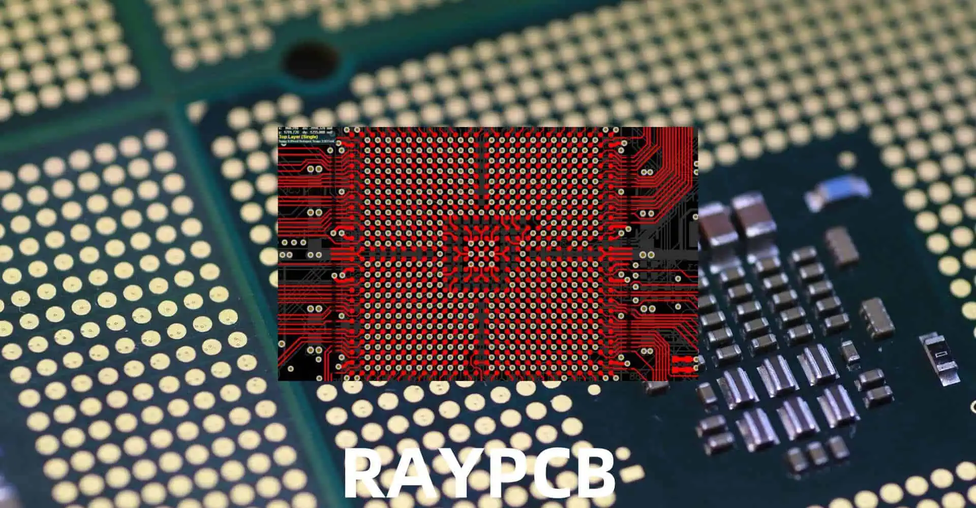
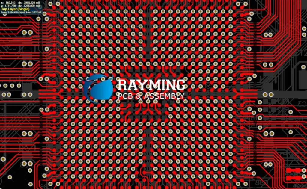
Aperture design significantly impacts paste release and print quality. The aperture size, shape, and wall finish all contribute to the effectiveness of paste transfer from stencil to PCB. Aperture walls should be smooth and properly finished to facilitate clean paste release. The aspect ratio, defined as the ratio of aperture width to stencil thickness, should typically be maintained above 1:1.5 for optimal paste release. Trapezoidal apertures, where the opening is slightly larger on the PCB side, can improve paste release characteristics.

Stencil material selection affects both durability and print quality. Stainless steel stencils offer excellent durability and precise aperture definition, while electroformed nickel stencils provide superior aperture wall smoothness and are particularly beneficial for fine-pitch applications. The choice between laser-cut and electroformed stencils depends on the specific requirements of aperture size, pitch, and production volume.

Solder Paste Properties

The rheological properties of solder paste significantly influence print quality and consistency. Viscosity affects the paste’s flow characteristics during printing and its ability to maintain shape after printing. Paste that is too thick may not flow properly through stencil apertures, resulting in incomplete fills or poor edge definition. Conversely, paste that is too thin may slump after printing, leading to bridging or poor print definition.

Particle size distribution within the solder paste affects both printability and final joint quality. Smaller particles generally provide better printability for fine-pitch applications but may exhibit different reflow characteristics. The metal content percentage influences both the mechanical properties of the printed deposit and the final solder joint strength. Higher metal content typically provides better electrical and mechanical properties but may affect printability.

Tackiness and working time are critical paste properties that affect handling and assembly processes. Adequate tackiness ensures component placement stability, while appropriate working time allows for process flexibility without degrading print quality. The paste’s thixotropic properties enable it to flow during printing while maintaining shape after deposition.

PCB Surface Conditions

The condition of the PCB surface finish dramatically affects solder paste adhesion and print quality. Common surface finishes include Hot Air Solder Leveling (HASL), Electroless Nickel Immersion Gold (ENIG), Immersion Silver, and Organic Solderability Preservative (OSP). Each finish presents different characteristics in terms of flatness, solderability, and shelf life that can impact paste printing.

Surface cleanliness is paramount for achieving consistent print quality. Contamination from oils, oxidation, or residual materials can prevent proper paste adhesion and lead to print defects. The PCB should be free from fingerprints, flux residues, and other contaminants that could interfere with paste adhesion.

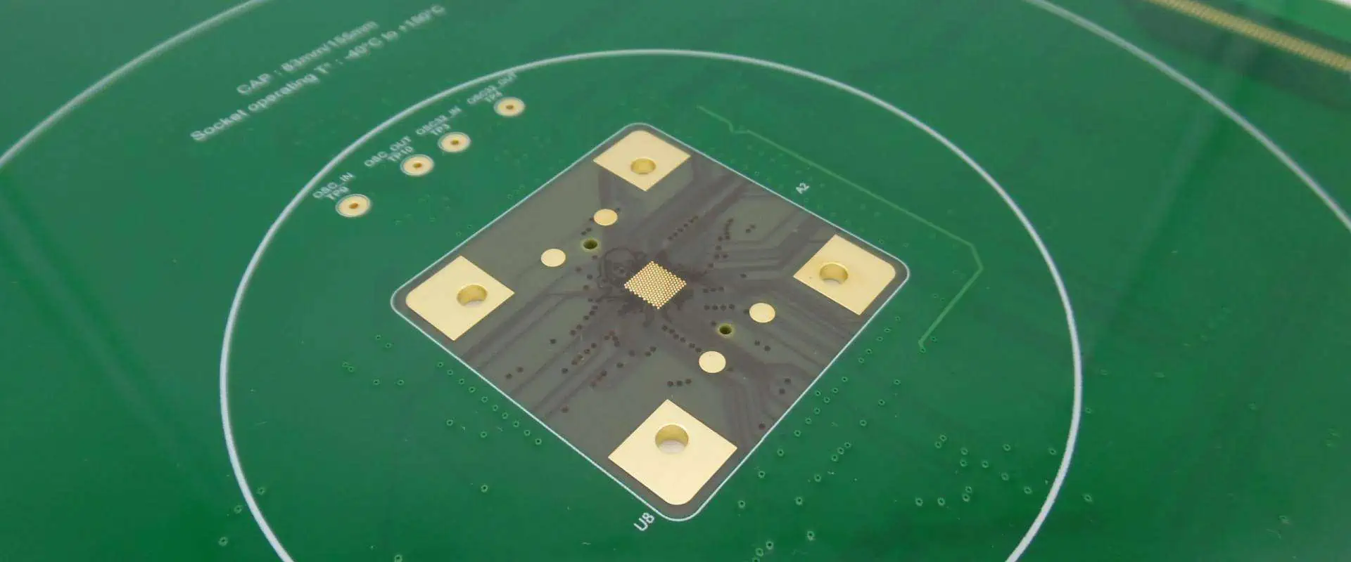
Pad design and layout significantly influence print quality. Pad size, shape, and spacing must be carefully considered in relation to the stencil aperture design. Proper registration between stencil apertures and PCB pads is essential for achieving accurate paste placement. Thermal relief connections and copper pour proximity can affect local heat dissipation during reflow, influencing joint formation.

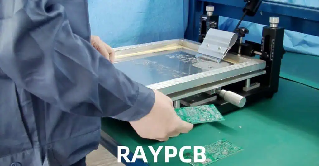
Printing Process Parameters

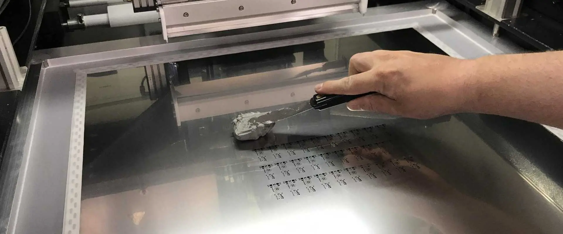
Squeegee pressure represents a critical process parameter that must be carefully controlled. Excessive pressure can force paste through apertures too aggressively, leading to paste bleeding under the stencil or poor edge definition. Insufficient pressure may result in incomplete aperture filling and inconsistent paste deposits. The optimal pressure typically ranges from 0.2 to 0.6 pounds per linear inch of squeegee length.

Print speed affects both the quality and throughput of the printing process. Slower speeds generally provide better aperture filling and more consistent deposits but reduce production efficiency. Faster speeds may improve throughput but can lead to inadequate filling of smaller apertures or poor paste release. The optimal speed typically ranges from 10 to 50 mm/second, depending on paste properties and stencil design.

Separation parameters, including snap-off distance and separation speed, critically affect paste release from the stencil. Proper separation ensures clean paste transfer while preventing smearing or distortion of the printed deposits. The snap-off distance should be minimized while maintaining adequate clearance for PCB warpage. Separation speed should be fast enough to ensure clean release but not so fast as to cause paste distortion.

Environmental Factors

Temperature and humidity significantly impact both solder paste properties and print quality. Higher temperatures generally reduce paste viscosity, improving flow characteristics but potentially affecting working time and print definition. Lower temperatures may increase viscosity, making printing more difficult but potentially improving print stability. Humidity affects paste properties and can lead to oxidation or other chemical changes that degrade print quality.

Atmospheric conditions in the printing environment should be controlled to maintain consistent paste properties. Excessive air movement can accelerate solvent evaporation from the paste, leading to changes in viscosity and printability. Dust and airborne contaminants can settle on the PCB surface or stencil, affecting print quality.

Equipment Considerations

Printer alignment and setup accuracy directly affect print quality and consistency. Proper registration between the stencil and PCB ensures accurate paste placement on the intended pads. Vision systems help maintain consistent registration and can detect and correct for minor variations in PCB placement.

Stencil support and tensioning systems affect print consistency and stencil life. Proper support prevents stencil deflection during printing, while appropriate tensioning maintains stencil flatness and prevents distortion. Inadequate support or tensioning can lead to inconsistent print thickness and poor edge definition.

Squeegee condition and maintenance significantly impact print quality. Worn or damaged squeegees can leave streaks, cause inconsistent pressure distribution, or fail to maintain proper contact with the stencil surface. Regular inspection and replacement of squeegees are essential for maintaining consistent print quality.

Quality Control and Monitoring

Implementing effective quality control measures is essential for maintaining consistent print quality. Solder paste inspection systems can detect defects such as insufficient paste volume, bridging, or misalignment before components are placed. These systems provide immediate feedback on print quality and can trigger process adjustments when necessary.

Statistical process control techniques help identify trends and variations in print quality over time. Monitoring key parameters such as paste volume, print thickness, and registration accuracy enables proactive process optimization and helps prevent quality issues before they affect production.

Regular maintenance and calibration of printing equipment ensure continued optimal performance. This includes cleaning stencils, replacing worn squeegees, calibrating vision systems, and verifying printer mechanics. Preventive maintenance schedules help minimize unexpected downtime and maintain consistent print quality.

The optimization of SMT solder paste print quality requires careful attention to multiple interconnected factors. Success depends on understanding the relationships between stencil design, paste properties, PCB conditions, process parameters, and environmental factors. By systematically addressing each of these areas and implementing appropriate quality control measures, manufacturers can achieve consistent, high-quality solder paste printing that forms the foundation for reliable electronic assemblies.

The Importance of Laminates for PCBs: Foundation of Modern Electronics

PCB Laminate Material Suppliers

Printed Circuit Boards (PCBs) form the backbone of virtually every electronic device in our modern world, from smartphones and computers to automotive systems and medical equipment. At the heart of every PCB lies a critical component that often goes unnoticed but plays an indispensable role in determining the board’s performance, reliability, and functionality: the laminate substrate. Understanding the importance of laminates for PCBs is essential for anyone involved in electronics design, manufacturing, or quality assurance.

YouTube video

What Are PCB Laminates?

PCB laminates are composite materials that serve as the foundational substrate upon which electronic circuits are built. These materials typically consist of a reinforcing material, such as fiberglass cloth, combined with a resin system that binds the layers together. The most common type is FR4 (Flame Retardant 4), which combines woven fiberglass cloth with epoxy resin to create a rigid, electrically insulating base material.

The laminate provides the structural foundation that supports copper traces, component mounting pads, and through-hole vias. Without a proper laminate substrate, it would be impossible to create the complex, multi-layered circuit patterns that modern electronics require. The laminate essentially acts as both a mechanical support structure and an electrical insulator, separating different circuit layers while maintaining the precise dimensional stability necessary for reliable electrical connections.

Mechanical Properties and Structural Integrity

Fr4 Laminate
Fr4 Laminate

One of the primary functions of PCB laminates is to provide mechanical strength and dimensional stability to the circuit board. Modern electronic devices are subject to various mechanical stresses, including vibration, thermal cycling, shock, and bending forces. The laminate must withstand these stresses while maintaining the precise positioning of electrical components and traces.

The mechanical properties of laminates directly impact the PCB’s ability to survive manufacturing processes such as drilling, routing, and component assembly. During drilling operations for through-holes and vias, the laminate must resist delamination and provide clean, burr-free holes. Poor-quality laminates can lead to drill smear, where resin material smears across the hole walls, potentially causing electrical connectivity issues.

Flexural strength and modulus are critical mechanical properties that determine how well a PCB can withstand bending stresses without cracking or breaking. In applications such as flexible PCB or boards that must fit into curved enclosures, the laminate’s mechanical properties become even more crucial. The coefficient of thermal expansion (CTE) is another vital mechanical characteristic, as mismatched CTE values between the laminate and copper can lead to stress buildup and potential failure during temperature cycling.

Electrical Performance Characteristics

The electrical properties of PCB laminates significantly influence signal integrity, power delivery, and overall circuit performance. Dielectric constant (Dk) and dissipation factor (Df) are two fundamental electrical characteristics that determine how electrical signals propagate through the PCB.

The dielectric constant affects the impedance of transmission lines and the propagation delay of signals. In high-speed digital circuits, maintaining consistent impedance is crucial for preventing signal reflections, crosstalk, and electromagnetic interference. Laminates with stable dielectric constants across frequency and temperature ranges enable designers to create controlled impedance structures that ensure reliable signal transmission.

Dissipation factor, also known as loss tangent, represents the amount of electrical energy lost as heat when an alternating electric field is applied to the material. Low-loss laminates are essential for high-frequency applications, such as RF circuits and high-speed digital systems, where signal attenuation must be minimized to maintain signal quality over long traces or at high frequencies.

Volume resistivity and surface resistivity are additional electrical properties that affect the laminate’s ability to prevent unwanted current paths and maintain electrical isolation between different circuit elements. High resistivity values are generally desirable to prevent leakage currents and ensure proper circuit operation.

Thermal Management and Heat Dissipation

Modern electronic devices generate significant amounts of heat, making thermal management a critical design consideration. PCB laminates play a crucial role in thermal management by providing pathways for heat dissipation and maintaining structural integrity at elevated temperatures.

The thermal conductivity of the laminate affects how efficiently heat can be conducted away from heat-generating components to heat sinks or other cooling mechanisms. Standard FR4 laminates have relatively low thermal conductivity, which can be limiting in high-power applications. Specialized laminates with enhanced thermal conductivity, such as metal-core PCBs or thermally conductive dielectrics, are often employed in LED lighting, power electronics, and other applications where efficient heat removal is essential.

Glass transition temperature (Tg) is a critical thermal property that defines the temperature at which the laminate begins to soften and lose its mechanical properties. Operating above the Tg can lead to dimensional instability, increased CTE, and potential delamination. High-Tg laminates are necessary for applications that must operate at elevated temperatures or undergo high-temperature assembly processes such as lead-free soldering.

Thermal decomposition temperature (Td) represents the temperature at which the laminate material begins to chemically break down. This property is particularly important during manufacturing processes that involve high temperatures, such as multiple reflow soldering cycles in complex assemblies.

Chemical Resistance and Environmental Durability

PCBs often operate in challenging environmental conditions, including exposure to chemicals, humidity, and various atmospheric contaminants. The laminate material must provide adequate chemical resistance to prevent degradation that could compromise electrical performance or mechanical integrity.

Moisture absorption is a critical concern, as absorbed water can affect electrical properties, cause dimensional changes, and lead to reliability issues such as conductive anodic filament (CAF) formation. CAF occurs when metal ions migrate through the laminate material in the presence of moisture and electrical bias, potentially creating conductive paths that can cause electrical failures.

The laminate’s resistance to various chemicals, including cleaning solvents, flux residues, and industrial chemicals, determines the PCB’s suitability for different applications. Medical devices, automotive systems, and industrial equipment often require laminates with enhanced chemical resistance to ensure long-term reliability in harsh environments.

Manufacturing Considerations and Processability

Rogers TMM 10i Laminate

The choice of laminate material significantly impacts PCB manufacturing processes and yields. Laminates must be compatible with various manufacturing steps, including drilling, plating, etching, and lamination processes.

Drill-ability is a crucial manufacturing consideration, as modern PCBs often require thousands of small-diameter holes for vias and component mounting. The laminate must provide clean drilling without excessive tool wear, delamination, or drill wander. Glass content, resin type, and filler materials all affect drill-ability and hole quality.

Plating adhesion is another critical factor, as the copper plating in through-holes and vias must form reliable bonds with the laminate material. Poor adhesion can lead to barrel cracking, via failures, and reliability issues. The laminate surface must be properly prepared and compatible with the plating chemistry to ensure strong metallization adhesion.

During the lamination process, where multiple layers are bonded together under heat and pressure, the laminate material must flow properly to fill voids and create strong interlayer bonds. Prepreg (pre-impregnated) materials must have the right resin content and flow characteristics to achieve void-free lamination while maintaining precise layer registration.

Advanced Laminate Technologies and Future Trends

As electronic systems become more complex and demanding, advanced laminate technologies continue to evolve to meet new requirements. Low-loss materials for 5G and millimeter-wave applications require extremely low dissipation factors and stable electrical properties at high frequencies. These materials often incorporate specialized resin systems and low-loss reinforcement materials.

Flexible and rigid-flex laminates enable new form factors and improved reliability by eliminating connectors and allowing three-dimensional circuit routing. These materials must combine flexibility with electrical performance and long-term reliability under repeated flexing.

Embedded component technologies integrate passive components directly into the laminate layers, enabling higher component density and improved electrical performance. These approaches require specialized laminate materials and manufacturing processes to maintain component functionality and reliability.

Environmental considerations are driving the development of halogen-free and recyclable laminate materials. These eco-friendly alternatives must maintain the performance characteristics required for reliable PCB operation while reducing environmental impact.

Conclusion

PCB laminates represent far more than simple substrate materials; they are sophisticated engineered composites that enable the functionality of modern electronic systems. Their mechanical, electrical, thermal, and chemical properties directly impact circuit performance, manufacturing yield, and long-term reliability. As electronic systems continue to evolve toward higher speeds, greater complexity, and more demanding operating conditions, the importance of selecting appropriate laminate materials becomes increasingly critical.

Understanding laminate properties and their impact on PCB performance enables engineers to make informed design decisions that optimize system performance while ensuring manufacturability and reliability. The continuous development of advanced laminate technologies promises to support the next generation of electronic innovations, from high-speed computing and 5G communications to electric vehicles and renewable energy systems. In this context, PCB laminates will continue to play a foundational role in enabling technological advancement and improving the quality of life through better electronic systems.

The Importance of DFMA Procedures for PCBs: Optimizing Design for Manufacturing Excellence

Design for Manufacturing and Assembly (DFMA) represents a critical methodology in modern electronics development, particularly for printed circuit boards (PCBs). This systematic approach integrates manufacturing and assembly considerations directly into the design phase, fundamentally transforming how engineers approach PCB development. By incorporating DFMA procedures early in the design process, organizations can achieve significant improvements in product quality, cost efficiency, and time-to-market while reducing manufacturing defects and assembly complications.

YouTube video

Understanding DFMA in the PCB Context

DFMA combines two complementary methodologies: Design for Manufacturing (DFM) and Design for Assembly (DFA). In PCB applications, DFM focuses on optimizing the board’s physical design to streamline fabrication processes, while DFA emphasizes simplifying component placement and assembly procedures. This dual approach addresses the entire production lifecycle, from raw material processing through final product assembly and testing.

The complexity of modern PCBs, with their increasingly dense component layouts, multilayer structures, and miniaturized form factors, makes DFMA procedures essential rather than optional. Today’s electronics demand high-density interconnects, fine-pitch components, and sophisticated routing architectures that push manufacturing capabilities to their limits. Without proper DFMA implementation, these advanced designs can result in prohibitively expensive manufacturing processes, unacceptable yield rates, and extended development timelines.

Cost Optimization Through Strategic Design Decisions

One of the most compelling arguments for implementing DFMA procedures lies in their profound impact on manufacturing costs. Studies consistently demonstrate that design decisions made during the initial phases of product development influence 70-80% of total manufacturing costs. By applying DFMA principles, engineers can identify and eliminate cost drivers before they become embedded in the final design.

Component selection represents a primary area where DFMA procedures deliver substantial cost benefits. Rather than choosing components based solely on electrical performance specifications, DFMA-guided selection considers factors such as component availability, standardization opportunities, and assembly complexity. This approach often reveals that slightly different components with similar electrical characteristics can dramatically reduce manufacturing costs through improved automation compatibility or reduced handling requirements.

Manufacturing process optimization through DFMA extends beyond component selection to encompass board design decisions that directly impact fabrication costs. Layer count optimization, via size and spacing specifications, drill hole sizing, and material selection all significantly influence manufacturing expenses. DFMA procedures provide structured frameworks for evaluating these trade-offs, enabling designers to make informed decisions that balance performance requirements with cost constraints.

Quality Enhancement and Defect Reduction

PCB DFM

DFMA procedures serve as powerful quality enhancement tools by systematically identifying and eliminating design features that contribute to manufacturing defects. Many common PCB quality issues, including solder joint failures, component misalignment, and thermal stress problems, originate from design decisions that inadequately consider manufacturing realities.

Solder joint reliability, a critical factor in PCB longevity, benefits significantly from DFMA-guided pad design optimization. Proper pad sizing, shape selection, and thermal relief implementation can dramatically improve solder joint formation and long-term reliability. DFMA procedures provide guidelines for optimizing these parameters based on component types, assembly processes, and operational requirements.

Component placement optimization through DFMA procedures addresses another major source of quality issues. By considering factors such as thermal interactions, mechanical stress distributions, and assembly sequence requirements, designers can create layouts that minimize component stress and improve overall reliability. This systematic approach often reveals placement conflicts that might otherwise remain undetected until prototype testing or production phases.

Manufacturing Process Compatibility and Efficiency

Modern PCB manufacturing involves numerous specialized processes, each with specific requirements and limitations. DFMA procedures ensure that design decisions align with these manufacturing capabilities, preventing costly redesigns and production delays. This compatibility extends across the entire manufacturing chain, from board fabrication through component placement, soldering, and final testing.

Assembly process optimization represents a particularly important aspect of DFMA implementation. Automated assembly equipment, including pick-and-place machines and wave soldering systems, operates most efficiently when PCB designs accommodate their specific capabilities and limitations. DFMA procedures provide structured approaches for optimizing component orientations, placement sequences, and assembly accessibility to maximize automation efficiency.

Testability considerations within DFMA frameworks ensure that completed assemblies can be efficiently verified and debugged. This includes providing adequate test point access, minimizing test fixture complexity, and incorporating design features that facilitate automated testing procedures. These considerations, when implemented early in the design process, can significantly reduce testing costs and improve production throughput.

Risk Mitigation and Design Robustness

DFMA procedures function as comprehensive risk management tools by identifying potential manufacturing and assembly challenges before they impact production schedules or product quality. This proactive approach enables design teams to address issues during the development phase when modifications are relatively inexpensive and schedule impacts are minimal.

Supply chain risk mitigation represents an increasingly important aspect of DFMA implementation. By considering component availability, alternate sourcing options, and end-of-life considerations during the design phase, engineers can create more resilient designs that maintain manufacturability despite supply chain disruptions. This strategic approach has proven particularly valuable in recent years as global supply chain challenges have impacted electronics manufacturing worldwide.

Design robustness improvements through DFMA extend beyond component selection to encompass layout optimization for manufacturing variations. Real-world manufacturing processes involve inherent variability in component placement accuracy, solder paste deposition, and thermal profiles. DFMA procedures help designers create layouts that maintain functionality despite these normal manufacturing variations, resulting in higher yield rates and more consistent product performance.

Implementation Strategies and Best Practices

Successful DFMA implementation requires systematic integration into existing design workflows rather than treatment as an afterthought or checklist exercise. This integration typically begins with establishing clear design rules and guidelines that reflect both manufacturing capabilities and cost targets. These rules should be regularly updated to reflect evolving manufacturing technologies and capability improvements.

Cross-functional collaboration represents a critical success factor for DFMA implementation. Effective programs involve manufacturing engineers, assembly technicians, quality personnel, and procurement specialists in the design review process. This collaborative approach ensures that all relevant manufacturing perspectives are considered and that design decisions reflect comprehensive understanding of production requirements.

Design review procedures should incorporate formal DFMA evaluation criteria alongside traditional electrical and mechanical verification processes. These reviews should occur at multiple project phases, allowing for iterative optimization as designs evolve and requirements become more clearly defined. Early-phase reviews focus on architectural decisions and component selection strategies, while later reviews address detailed layout optimization and assembly sequence planning.

Future Considerations and Emerging Technologies

As PCB technologies continue evolving toward higher densities, faster signal speeds, and more complex integration requirements, DFMA procedures must adapt to address new manufacturing challenges. Emerging technologies such as embedded components, flexible-rigid constructions, and advanced packaging techniques introduce new variables that must be incorporated into DFMA frameworks.

Artificial intelligence and machine learning technologies are beginning to enhance DFMA implementation by automating routine design optimization tasks and identifying optimization opportunities that might be overlooked by manual analysis. These tools can process vast amounts of manufacturing data to identify patterns and correlations that inform design decisions and improve manufacturing predictability.

The increasing emphasis on sustainability and environmental responsibility is also influencing DFMA procedures, with growing focus on material selection, end-of-life considerations, and manufacturing process environmental impacts. Future DFMA implementations will likely incorporate comprehensive lifecycle assessment criteria alongside traditional cost and quality metrics.

Conclusion

DFMA procedures represent essential methodologies for modern PCB development, delivering measurable improvements in cost efficiency, product quality, manufacturing reliability, and time-to-market performance. Their systematic approach to integrating manufacturing considerations into design decisions helps organizations navigate the increasing complexity of modern electronics while maintaining competitive advantages in rapidly evolving markets.

The investment in comprehensive DFMA implementation pays dividends throughout the product lifecycle, from reduced development costs and shorter design cycles through improved manufacturing yields and enhanced product reliability. As PCB technologies continue advancing and manufacturing requirements become increasingly sophisticated, organizations that embrace DFMA principles will be better positioned to succeed in competitive electronics markets while delivering superior products to their customers.

Difference Between DFA and DFM for PCBs: A Comprehensive Guide

The success of printed circuit board (PCB) manufacturing depends heavily on two critical design methodologies: Design for Assembly (DFA) and Design for Manufacturing (DFM). While these terms are often used interchangeably or confused with one another, they represent distinct yet complementary approaches that address different aspects of the PCB production process. Understanding the fundamental differences between DFA and DFM is essential for engineers, designers, and manufacturers who want to optimize their PCB designs for cost-effectiveness, reliability, and manufacturability.

YouTube video

Understanding Design for Manufacturing (DFM)

Design for Manufacturing (DFM) focuses on optimizing the PCB design to make the manufacturing process as efficient, cost-effective, and error-free as possible. DFM principles are applied during the design phase to ensure that the bare PCB can be fabricated successfully using standard manufacturing processes and equipment. The primary goal is to create a design that can be manufactured consistently with high yield rates while minimizing production costs and lead times.

DFM considerations for PCBs encompass various aspects of the bare board fabrication process. Trace width and spacing requirements are fundamental DFM concerns, as they must comply with the capabilities of the chosen PCB fabrication facility. Minimum trace widths, via sizes, and spacing between conductors must be carefully considered to ensure the board can be manufactured reliably. Layer stackup design is another crucial DFM element, where engineers must balance electrical performance requirements with manufacturing constraints such as available prepreg thicknesses and copper weights.

Material selection plays a significant role in DFM optimization. Choosing standard materials and thicknesses that are readily available from PCB manufacturers can significantly reduce costs and lead times compared to exotic or custom materials. Additionally, DFM principles guide decisions about hole sizes, drill aspects ratios, and the placement of vias to ensure they can be reliably drilled and plated during fabrication.

The DFM process also involves considerations for panelization, where multiple PCBs are arranged on a single panel for efficient manufacturing. Proper panel design includes adequate spacing between boards, appropriate tooling holes, and fiducial markers for automated handling equipment. Surface finish selection, such as HASL, ENIG, or OSP, is another DFM consideration that affects both manufacturability and end-use performance.

Understanding Design for Assembly (DFA)

Design for Assembly (DFA) focuses specifically on optimizing the PCB design to facilitate the efficient and reliable assembly of electronic components onto the manufactured board. While DFM addresses the fabrication of the bare PCB, DFA is concerned with the subsequent process of component placement, soldering, and final assembly operations. The primary objective of DFA is to minimize assembly time, reduce assembly costs, improve yield rates, and enhance the overall reliability of the assembled product.

DFA principles heavily influence component selection, placement, and orientation decisions. Component footprint design must accommodate the capabilities of pick-and-place equipment, ensuring that components can be accurately positioned during automated assembly. This includes considerations for component package types, with preference often given to surface-mount devices (SMDs) over through-hole components due to their compatibility with high-speed automated assembly processes.

Solder joint accessibility and inspectability are key DFA concerns. Components must be positioned to allow proper solder joint formation and enable both automated optical inspection (AOI) and manual visual inspection. This involves maintaining adequate spacing between components, avoiding component shadowing that could interfere with inspection processes, and ensuring that critical solder joints remain visible and accessible.

Thermal management during assembly is another important DFA consideration. Large components or heat sinks can create thermal shadows during reflow soldering, potentially leading to poor solder joint formation for nearby components. DFA principles guide the placement of components to ensure uniform heating during the soldering process and may influence decisions about component orientation and spacing.

Test point accessibility represents a crucial DFA element, as assembled boards must often undergo electrical testing. DFA guidelines ensure that test points are properly positioned and accessible to testing equipment, facilitating efficient in-circuit testing and functional verification procedures.

Key Differences in Focus and Scope

The fundamental difference between DFA and DFM lies in their respective focus areas within the PCB production workflow. DFM is primarily concerned with the fabrication of the bare PCB substrate, addressing challenges related to etching, drilling, plating, and other board manufacturing processes. DFA, conversely, focuses on the assembly phase, where electronic components are mounted and soldered onto the fabricated PCB.

This distinction in focus leads to different optimization priorities. DFM optimization typically emphasizes factors such as manufacturability margins, yield improvement in PCB fabrication, and cost reduction in substrate production. DFA optimization prioritizes assembly efficiency, component placement accessibility, soldering reliability, and testing convenience.

The timing of implementation also differs between these approaches. DFM considerations must be addressed early in the design process, as they fundamentally affect the PCB stackup, layer count, material selection, and physical board characteristics. Once the board is fabricated, most DFM-related parameters cannot be changed. DFA considerations, while also best addressed during initial design phases, can sometimes be modified through component selection changes or placement adjustments even after initial board fabrication.

Impact on Design Decisions

DFM and DFA principles often influence different aspects of PCB design decisions, though some overlap exists. DFM heavily influences decisions about copper thickness, dielectric materials, via structures, and minimum feature sizes. These parameters directly affect the PCB fabrication process and must align with the capabilities of the chosen manufacturing facility.

DFA principles primarily influence component selection, placement strategies, and assembly-related design features. This includes decisions about component package types, orientation requirements, spacing constraints, and the inclusion of assembly aids such as fiducial markers and tooling holes.

Sometimes DFM and DFA requirements can conflict, requiring design compromises. For example, DFM might prefer larger via sizes for better manufacturability, while DFA might prefer smaller vias to maximize routing density and component placement flexibility. Successful PCB design requires balancing these potentially competing requirements to achieve an optimal overall solution.

Implementation Strategies

Effective implementation of both DFM and DFA requires close collaboration between design teams and manufacturing partners. DFM implementation typically involves early engagement with PCB fabrication houses to understand their specific capabilities, limitations, and preferences. This collaboration helps establish design rules that align with manufacturing capabilities while meeting electrical and mechanical requirements.

DFA implementation requires similar collaboration with assembly houses, component suppliers, and testing facilities. Understanding the capabilities and limitations of pick-and-place equipment, reflow ovens, and testing systems helps inform design decisions that optimize assembly efficiency and reliability.

Many organizations implement DFM and DFA through formal design review processes, where manufacturing and assembly partners evaluate designs before production begins. These reviews help identify potential issues early in the development cycle when changes are less costly and time-consuming to implement.

Economic Implications

The economic impact of proper DFM and DFA implementation can be substantial. Effective DFM can reduce PCB fabrication costs through improved yields, reduced scrap rates, and shortened production cycles. It can also minimize the need for expensive manufacturing processes or exotic materials, leading to significant cost savings in high-volume production.

Similarly, proper DFA implementation can dramatically reduce assembly costs through faster placement times, higher first-pass yields, and reduced rework requirements. The cumulative effect of small improvements in assembly efficiency can result in significant cost savings when multiplied across thousands or millions of units.

Conclusion

While DFA and DFM are complementary approaches that both contribute to successful PCB production, understanding their distinct focus areas and requirements is essential for optimal design outcomes. DFM addresses the challenges of bare board fabrication, emphasizing manufacturability, yield, and cost optimization in PCB substrate production. DFA focuses on assembly efficiency, component placement optimization, and testing accessibility in the component mounting and soldering phases.

Successful PCB design requires careful consideration of both DFM and DFA principles, often requiring trade-offs and compromises to balance competing requirements. By understanding these differences and implementing both approaches systematically, engineers can create PCB designs that are not only electrically and mechanically sound but also optimized for efficient, cost-effective manufacturing and assembly. The investment in proper DFM and DFA implementation pays dividends through reduced production costs, improved quality, shorter development cycles, and enhanced product reliability in the marketplace.

BGA ROUTING AND IMPEDANCE CONTROL IN HDI PCBs

In the rapidly evolving world of electronics, High-Density Interconnect (HDI) Printed Circuit Boards (PCBs) have become crucial for meeting the demands of miniaturization and increased functionality. Among the challenges faced by PCB designers, Ball Grid Array (BGA) routing and impedance control stand out as critical aspects that significantly impact the performance and reliability of electronic devices. This article delves into the intricacies of BGA routing and impedance control in HDI PCBs, exploring best practices, challenges, and emerging technologies in this field.

YouTube video

Understanding BGA Technology

What is BGA?

Ball Grid Array (BGA) is a surface-mount packaging technology for integrated circuits. It is designed to address the increasing demand for higher pin counts and better electrical and thermal performance in a compact form factor.

Advantages of BGA

  1. Higher pin count in a smaller area
  2. Better thermal and electrical performance
  3. Reduced lead inductance
  4. Improved reliability due to self-alignment during reflow

Types of BGA Packages

BGA TypeDescriptionTypical Application
Plastic BGA (PBGA)Uses plastic substrateConsumer electronics
Ceramic BGA (CBGA)Uses ceramic substrateHigh-reliability applications
Tape BGA (TBGA)Uses polyimide tape substrateLightweight applications
Micro BGA (BGA)Smaller pitch, typically < 0.8mmMobile devices
Flip Chip BGA (FCBGA)Die is flipped and connected directly to substrateHigh-performance computing

HDI PCB Technology

Definition of HDI

High-Density Interconnect (HDI) PCBs are characterized by higher wiring density per unit area. They typically feature finer lines and spaces, smaller vias and capture pads, and higher connection pad density than traditional PCBs.

Key Features of HDI PCBs

  1. Microvias (laser-drilled vias with diameter < 150ยตm)
  2. Fine line width and spacing (typically < 100ยตm)
  3. High layer count (often > 10 layers)
  4. Buried and blind vias
  5. Sequential lamination process

Benefits of HDI in BGA Routing

  1. Improved signal integrity
  2. Reduced board size and weight
  3. Enhanced electrical performance
  4. Better thermal management
  5. Increased design flexibility

BGA Routing Strategies in HDI PCBs

Fanout Techniques

1. Dog Bone Fanout

  • Description: Uses short traces (“dog bones”) to connect BGA pads to vias
  • Pros: Simple, cost-effective
  • Cons: Limited routing density, longer signal paths

2. Via-in-Pad

  • Description: Vias placed directly in BGA pads
  • Pros: Highest density, shortest signal paths
  • Cons: More complex manufacturing, potential reliability issues

3. Via-near-Pad

  • Description: Vias placed adjacent to BGA pads
  • Pros: Balance between density and manufacturability
  • Cons: Slightly longer signal paths than via-in-pad

Layer Stack-up Considerations

  1. Signal layer allocation
  2. Power and ground plane placement
  3. Microvia structure (stacked, staggered, or skip vias)

Routing Guidelines

  1. Maintain consistent trace widths
  2. Use 45-degree angles for direction changes
  3. Implement differential pair routing for high-speed signals
  4. Avoid routing under BGA to minimize crosstalk
  5. Consider signal grouping and length matching

Impedance Control in HDI PCBs

Importance of Impedance Control

Impedance control is crucial for maintaining signal integrity, especially in high-speed designs. It helps minimize signal reflections, reduce electromagnetic interference (EMI), and ensure proper signal transmission.

Factors Affecting Impedance

  1. Trace width
  2. Trace thickness
  3. Dielectric constant of PCB material
  4. Distance to reference planes
  5. Presence of nearby conductors

Common Impedance Values

ApplicationTypical Impedance
Single-ended50ฮฉ or 75ฮฉ
Differential100ฮฉ or 120ฮฉ
USB90ฮฉ differential
HDMI100ฮฉ differential
PCIe100ฮฉ differential

Impedance Calculation

While exact impedance calculations can be complex, a simplified formula for microstrip impedance is:

Zโ‚€ = 87 / โˆš(ฮตแตฃ + 1.41) * ln(5.98h / (0.8w + t))

Where:

  • Zโ‚€ is the characteristic impedance
  • ฮตแตฃ is the dielectric constant of the PCB material
  • h is the height of the trace above the ground plane
  • w is the width of the trace
  • t is the thickness of the trace

Impedance Control Techniques

1. Controlled Dielectric Thickness

HDI PCB Board Laminate Structure-PCB Manufacturer-4
  • Maintain consistent dielectric thickness between signal layers and adjacent planes
  • Use high-quality, low-tolerance PCB materials

2. Trace Width Control

  • Adjust trace widths to achieve desired impedance
  • Use impedance calculators or field solvers for accurate calculations

3. Copper Weight Management

  • Consider the impact of copper thickness on impedance
  • Use consistent copper weights across the board

4. Reference Plane Design

  • Ensure solid, uninterrupted reference planes
  • Implement proper return path design

5. Differential Pair Routing

  • Maintain consistent spacing between differential pairs
  • Use serpentine routing for length matching

Challenges in BGA Routing and Impedance Control

1. High-Density Routing

  • Limited space for routing between BGA pads
  • Need for advanced PCB fabrication techniques

2. Signal Integrity

  • Managing crosstalk and EMI in dense layouts
  • Maintaining consistent impedance across the board

3. Thermal Management

  • Dealing with heat dissipation in high-pin-count BGAs
  • Balancing thermal and electrical requirements

4. Manufacturing Complexity

  • Increased cost due to more complex fabrication processes
  • Higher potential for manufacturing defects

5. Testing and Inspection

  • Limited access to BGA solder joints for inspection
  • Need for advanced testing techniques (e.g., X-ray inspection)

Advanced Techniques and Future Trends

1. 3D Routing

2. AI-Assisted Routing

  • Using machine learning algorithms for optimal trace routing
  • Automated impedance control and signal integrity analysis

3. Advanced Materials

  • Development of low-loss, high-speed PCB materials
  • Implementation of novel dielectrics for improved performance

4. Optical Interconnects

  • Integration of optical layers in HDI PCBs
  • Hybrid electro-optical routing solutions

5. Additive Manufacturing

  • 3D-printed PCBs with integrated BGA routing
  • Custom impedance control through additive processes

Best Practices for BGA Routing and Impedance Control

  1. Use appropriate design tools and simulators
  2. Implement a well-planned layer stack-up
  3. Follow manufacturer’s guidelines for BGA fanout
  4. Perform thorough signal integrity analysis
  5. Use controlled impedance techniques consistently
  6. Implement proper power distribution network (PDN) design
  7. Consider thermal management early in the design process
  8. Collaborate closely with PCB fabricators and assemblers
  9. Implement robust design for manufacturability (DFM) practices
  10. Conduct thorough testing and verification before production

Conclusion

BGA routing and impedance control in HDI PCBs represent critical challenges in modern electronic design. As devices continue to shrink in size while increasing in complexity and performance, mastering these aspects becomes essential for creating reliable, high-performance electronics.

The successful implementation of BGA routing and impedance control requires a deep understanding of PCB design principles, material properties, and manufacturing processes. Designers must balance the demands of high-density routing with the need for signal integrity, thermal management, and manufacturability.

As we look to the future, emerging technologies such as 3D routing, AI-assisted design, and advanced materials promise to push the boundaries of what’s possible in HDI PCB design. However, these advancements will also bring new challenges that designers must be prepared to address.

Ultimately, the key to success in BGA routing and impedance control lies in a holistic approach to PCB design, combining technical expertise with creativity and a willingness to embrace new technologies and methodologies. By following best practices and staying abreast of industry developments, designers can create HDI PCBs that meet the ever-increasing demands of modern electronics.

FAQ

Q1: What are the main advantages of using BGAs in HDI PCB designs?

A1: The main advantages of using BGAs in HDI PCB designs include:

  1. Higher pin count in a smaller area, allowing for more compact designs
  2. Improved electrical performance due to shorter interconnects and reduced parasitic effects
  3. Better thermal performance, as the entire bottom surface of the package can be used for heat dissipation
  4. Reduced lead inductance, which is crucial for high-speed applications
  5. Self-alignment during the reflow process, which can improve manufacturing yield
  6. More robust mechanical connection compared to leaded packages
  7. Ability to accommodate complex ICs with high I/O requirements

Q2: How does impedance control impact signal integrity in HDI PCBs?

A2: Impedance control significantly impacts signal integrity in HDI PCBs in several ways:

  1. Minimizes signal reflections: Consistent impedance along the signal path reduces reflections that can cause signal distortion.
  2. Reduces electromagnetic interference (EMI): Proper impedance control helps contain electromagnetic fields, reducing unwanted radiation and coupling.
  3. Improves signal quality: Controlled impedance environments maintain signal shape and timing, crucial for high-speed data transmission.
  4. Enhances power integrity: Well-controlled impedance in power distribution networks helps maintain stable power delivery to components.
  5. Enables faster edge rates: Consistent impedance allows for faster signal transition times without degradation.
  6. Facilitates matching: Controlled impedance makes it easier to match source, transmission line, and load impedances, maximizing power transfer.
  7. Supports higher bandwidth: By maintaining signal quality, impedance control enables higher data rates and bandwidth in digital systems.

Q3: What are the key challenges in routing high pin-count BGAs in HDI PCBs?

A3: Routing high pin-count BGAs in HDI PCBs presents several key challenges:

  1. Limited space: The high density of BGA pins leaves little room for routing between pads.
  2. Layer count management: Balancing the need for multiple routing layers with manufacturing constraints and cost considerations.
  3. Via management: Efficiently using and placing microvias to access inner layers without blocking too many routing channels.
  4. Signal integrity: Maintaining proper signal quality, especially for high-speed signals, in a dense routing environment.
  5. Power delivery: Ensuring adequate power and ground connections to all parts of the BGA.
  6. Thermal management: Dealing with heat dissipation in high-pin-count, densely routed areas.
  7. Manufacturability: Ensuring the design can be reliably manufactured and assembled despite its complexity.
  8. Impedance control: Maintaining consistent impedance in a constrained routing space.
  9. Crosstalk minimization: Managing electromagnetic coupling between closely spaced traces.
  10. Testability: Providing adequate test points and implementing design-for-test strategies in a limited-access environment.

Q4: How does the choice of PCB material affect impedance control in HDI designs?

A4: The choice of PCB material significantly affects impedance control in HDI designs in several ways:

  1. Dielectric constant: Materials with lower and more stable dielectric constants allow for more precise impedance control.
  2. Loss tangent: Lower loss tangent materials reduce signal attenuation, especially at high frequencies.
  3. Thickness control: Materials with tighter thickness tolerances enable more accurate impedance calculations and control.
  4. Thermal stability: Materials with lower coefficients of thermal expansion (CTE) maintain more consistent impedance across temperature ranges.
  5. Moisture absorption: Materials with lower moisture absorption rates maintain more stable electrical properties over time.
  6. Frequency dependence: Some materials maintain more consistent properties across a wide frequency range, crucial for broadband applications.
  7. Copper adhesion: Better copper adhesion allows for finer lines and spaces, enabling more precise impedance control.
  8. Homogeneity: More homogeneous materials provide more consistent electrical properties across the board.
  9. Cost: High-performance materials often come at a higher cost, requiring a balance between performance and budget.

Q5: What emerging technologies are likely to impact BGA routing and impedance control in the future?

A5: Several emerging technologies are poised to impact BGA routing and impedance control:

  1. 3D printing of PCBs: Enabling complex 3D routing strategies and custom impedance structures.
  2. AI-assisted routing: Using machine learning algorithms to optimize BGA breakout and routing patterns.
  3. Advanced PCB materials: Development of novel substrate materials with improved electrical and thermal properties.
  4. Embedded components: Integrating passive and active components within PCB layers to free up surface routing space.
  5. Optical interconnects: Incorporating optical layers in HDI PCBs for high-speed, low-loss signal transmission.
  6. Additive manufacturing techniques: Allowing for more precise control of trace geometries and material deposition.
  7. Advanced simulation tools: More accurate and efficient electromagnetic and thermal simulation capabilities.
  8. Photonic PCBs: Integration of optical waveguides with traditional PCB technology for ultra-high-speed applications.
  9. Flexible and stretchable electronics: New form factors requiring novel approaches to BGA mounting and impedance control.
  10. Quantum computing integration: Adapting PCB design for quantum computing requirements, including cryogenic operations and specialized signal routing.

CSP AND FINE-PITCH PCB ASSEMBLY

eMMC BGA

In the ever-evolving world of electronics, the demand for smaller, faster, and more powerful devices continues to drive innovation in printed circuit board (PCB) assembly techniques. Two key technologies at the forefront of this miniaturization trend are Chip Scale Packaging (CSP) and fine-pitch assembly. This article explores these cutting-edge approaches, their benefits, challenges, and their impact on the electronics manufacturing industry.

YouTube video

Understanding Chip Scale Packaging (CSP)

Definition and Characteristics

Chip Scale Packaging (CSP) is an advanced integrated circuit (IC) packaging technology where the package is no more than 1.2 times the size of the die. CSPs are designed to minimize the physical size of electronic components while maintaining or improving their performance.

Key characteristics of CSPs include:

  1. Small form factor
  2. Direct surface mountable
  3. Reduced parasitics
  4. Improved thermal performance
  5. Enhanced electrical characteristics

Types of CSP

1. Flip Chip CSP

Flip Chip
Flip Chip

Flip Chip CSP involves mounting the chip face-down on the substrate, with connections made through small solder bumps.

2. Wire Bonded CSP

In this type, the chip is connected to the package substrate using wire bonds before being encapsulated.

3. Wafer Level CSP (WLCSP)

WLCSP is created directly on the wafer before singulation, resulting in a package the same size as the die.

4. Stacked CSP

Multiple chips are stacked vertically within a single package, allowing for even greater miniaturization.

Advantages of CSP

  1. Reduced footprint and weight
  2. Improved electrical performance due to shorter interconnects
  3. Better thermal management
  4. Higher I/O density
  5. Cost-effective for high-volume production

Challenges in CSP Implementation

  1. Requires advanced assembly equipment
  2. More sensitive to thermal stress
  3. Increased complexity in PCB design
  4. Potential reliability issues due to smaller solder joints

Fine-Pitch PCB Assembly

Definition and Importance

Fine-pitch assembly refers to the process of placing and soldering components with very close lead spacing on a PCB. As electronic devices become smaller and more complex, the need for fine-pitch assembly has become crucial.

Fine-Pitch Categories

CategoryLead Pitch
Standard> 0.65 mm
Fine0.4 mm – 0.65 mm
Ultra-Fine0.3 mm – 0.4 mm
Super-Fine< 0.3 mm

Key Technologies in Fine-Pitch Assembly

1. Advanced Pick-and-Place Machines

Modern pick-and-place machines offer high accuracy and speed, capable of placing components with pitches as small as 0.3 mm or less.

2. High-Precision Stencil Printing

Stencil printing technology has evolved to accommodate fine-pitch requirements, with improvements in stencil materials, designs, and printing processes.

3. Reflow Soldering Optimization

Reflow profiles must be carefully optimized to ensure proper solder joint formation without causing component damage or solder bridging.

4. Automated Optical Inspection (AOI)

AOI systems play a crucial role in detecting defects in fine-pitch assemblies, offering high-resolution imaging and advanced algorithms for defect detection.

Challenges in Fine-Pitch Assembly

  1. Increased risk of solder bridging
  2. Difficulty in rework and repair
  3. Higher sensitivity to PCB warpage and coplanarity issues
  4. Stringent requirements for component placement accuracy
  5. Need for advanced inspection techniques

PCB Design Considerations for CSP and Fine-Pitch Assembly

Xilinx Versal FPGA
Xilinx Versal FPGA

Layout and Routing

  1. Careful planning of component placement
  2. Use of microvias and HDI techniques
  3. Consideration of signal integrity and power distribution
  4. Implementation of proper thermal management strategies

Solder Pad Design

  1. Optimization of pad size and shape
  2. Use of solder mask defined (SMD) vs. non-solder mask defined (NSMD) pads
  3. Implementation of proper pad finish (e.g., ENIG, HASL)

Design for Manufacturability (DFM)

  1. Adherence to minimum spacing rules
  2. Consideration of pick-and-place machine capabilities
  3. Design for testability and inspection

Material Selection

  1. Use of appropriate PCB substrate materials
  2. Selection of solder paste with suitable particle size and flux characteristics
  3. Consideration of underfill materials for certain CSP applications

Manufacturing Process for CSP and Fine-Pitch Assembly

1. PCB Fabrication

  • High-precision drilling and etching
  • Implementation of advanced PCB technologies (e.g., HDI, microvias)

2. Solder Paste Printing

  • Use of ultra-fine pitch stencils
  • Optimization of printing parameters (speed, pressure, separation speed)
  • Implementation of automated solder paste inspection (SPI)

3. Component Placement

  • Use of advanced pick-and-place machines with high accuracy
  • Implementation of fiducial marks for improved placement precision
  • Consideration of component-specific placement requirements

4. Reflow Soldering

  • Development of optimized reflow profiles
  • Use of nitrogen atmosphere for improved soldering results
  • Implementation of proper cooling strategies

5. Inspection and Quality Control

  • Automated optical inspection (AOI) for solder joint and placement verification
  • X-ray inspection for hidden solder joints (e.g., BGA, CSP)
  • Implementation of in-circuit testing (ICT) and functional testing

6. Rework and Repair (if necessary)

  • Use of specialized rework stations for CSP and fine-pitch components
  • Implementation of proper handling and ESD protection procedures

Advanced Techniques in CSP and Fine-Pitch Assembly

1. 3D Package Integration

  • Stacking of multiple CSPs
  • Integration of different component types within a single package

2. Embedded Components

  • Incorporation of passive and active components within PCB layers
  • Reduction of overall PCB size and improvement of electrical performance

3. Laser-Assisted Bonding

  • Use of laser technology for precise solder reflow
  • Enablement of ultra-fine pitch assembly

4. Plasma Cleaning

  • Implementation of plasma cleaning processes to improve solder joint reliability
  • Enhancement of surface wettability for improved solder paste adhesion

5. Conformal Coating

  • Application of protective coatings to improve reliability in harsh environments
  • Use of advanced coating materials and application techniques

Industry Trends and Future Outlook

xilinx-spartan-6-fpga-tutorial

Miniaturization Trends

The push for smaller, more powerful devices continues to drive the development of even smaller CSPs and finer pitch assemblies.

YearMinimum CSP SizeMinimum Lead Pitch
20200.4 mm x 0.4 mm0.3 mm
20220.3 mm x 0.3 mm0.25 mm
2024 (projected)0.2 mm x 0.2 mm0.2 mm
2026 (projected)0.15 mm x 0.15 mm0.15 mm

Integration with Advanced Technologies

  1. 5G and high-frequency applications
  2. Internet of Things (IoT) devices
  3. Artificial Intelligence (AI) and machine learning hardware
  4. Automotive electronics
  5. Wearable technology

Sustainability and Environmental Considerations

  1. Development of lead-free and halogen-free CSP solutions
  2. Implementation of more energy-efficient assembly processes
  3. Focus on recyclability and end-of-life considerations in package design

Automation and Industry 4.0

  1. Increased use of AI and machine learning in assembly processes
  2. Implementation of digital twin technology for process optimization
  3. Development of fully automated, lights-out manufacturing facilities

Conclusion

CSP and fine-pitch PCB assembly technologies have revolutionized the electronics industry, enabling the creation of smaller, more powerful devices that were once thought impossible. As we continue to push the boundaries of miniaturization, these technologies will play an increasingly critical role in shaping the future of electronics.

The challenges associated with CSP and fine-pitch assembly are significant, requiring ongoing innovation in materials, processes, and equipment. However, the benefits in terms of device performance, size reduction, and functionality make these challenges worth overcoming.

As the industry moves forward, we can expect to see even more advanced packaging solutions, finer pitches, and more integrated assemblies. The convergence of CSP and fine-pitch technologies with other emerging trends such as 3D integration, embedded components, and advanced materials will likely lead to new breakthroughs in electronic device design and manufacturing.

The future of CSP and fine-pitch PCB assembly is bright, promising continued innovation and exciting new possibilities in the world of electronics. As these technologies evolve, they will enable the next generation of electronic devices that will shape our increasingly connected and technology-driven world.

FAQ

Q1: What is the main difference between CSP and traditional IC packaging?

A1: The main difference lies in the size and efficiency of the package. Chip Scale Packaging (CSP) is designed to be very close to the size of the actual silicon die, typically no more than 1.2 times the size of the die. Traditional IC packages, on the other hand, are often significantly larger than the die they contain. CSPs offer several advantages, including:

  1. Smaller footprint on the PCB
  2. Improved electrical performance due to shorter interconnects
  3. Better thermal characteristics
  4. Higher I/O density
  5. Often more cost-effective for high-volume production

Q2: What are the key challenges in implementing fine-pitch PCB assembly?

A2: Implementing fine-pitch PCB assembly comes with several challenges:

  1. Increased risk of solder bridging due to closer component leads
  2. Higher demands on placement accuracy for pick-and-place machines
  3. Need for more precise stencil printing to control solder paste volume
  4. Difficulty in inspection and quality control due to smaller features
  5. Increased sensitivity to PCB warpage and coplanarity issues
  6. Challenges in rework and repair of defective joints
  7. Requirements for more advanced PCB design techniques, such as the use of microvias

Q3: How does the use of CSPs and fine-pitch assembly impact PCB design?

A3: The use of CSPs and fine-pitch assembly significantly impacts PCB design in several ways:

  1. Requires more careful component placement and routing to manage the higher density
  2. Often necessitates the use of advanced PCB technologies like High-Density Interconnect (HDI) and microvias
  3. Demands greater attention to signal integrity due to closer proximity of components
  4. Requires more sophisticated power distribution network design
  5. Necessitates careful thermal management strategies
  6. Calls for stricter adherence to design for manufacturability (DFM) guidelines
  7. Often requires the use of more advanced PCB materials to meet performance requirements

Q4: What are some emerging technologies that complement CSP and fine-pitch assembly?

A4: Several emerging technologies are complementing and enhancing CSP and fine-pitch assembly:

  1. 3D package integration, allowing for vertical stacking of multiple chips
  2. Embedded component technology, integrating passive and active components within PCB layers
  3. Advanced materials, such as low-loss dielectrics for high-frequency applications
  4. Laser-assisted bonding for ultra-fine pitch assembly
  5. Plasma cleaning processes to improve solder joint reliability
  6. Advanced inspection technologies, including high-resolution X-ray and 3D AOI systems
  7. AI and machine learning for process optimization and defect prediction

Q5: How is the industry addressing the environmental concerns related to CSP and fine-pitch assembly?

A5: The industry is addressing environmental concerns through several initiatives:

  1. Development of lead-free and halogen-free CSP solutions to comply with regulations like RoHS
  2. Implementation of more energy-efficient assembly processes to reduce carbon footprint
  3. Design for recyclability, considering end-of-life disassembly and material recovery
  4. Use of more environmentally friendly flux and cleaning agents in the assembly process
  5. Optimization of manufacturing processes to reduce waste and improve yield
  6. Development of more durable designs to extend product lifespan
  7. Implementation of circular economy principles in the electronics supply chain

Micro-Hole Technology for HDI PCBs

What is Micro-Hole Technology?

Micro-hole technology represents a revolutionary advancement in printed circuit board (PCB) manufacturing, specifically designed to meet the demanding requirements of High Density Interconnect (HDI) boards. This sophisticated drilling technique creates extremely small holes, typically ranging from 50 to 150 micrometers in diameter, which are significantly smaller than traditional mechanical drill holes that usually measure 200 micrometers or larger.

The technology enables manufacturers to create intricate interconnections between different layers of multilayer PCBs, allowing for unprecedented component density and miniaturization. These microscopic holes serve as pathways for electrical signals, connecting traces on different layers while occupying minimal board real estate.

YouTube video

Types of Micro-Holes in HDI PCBs

Microvias

Microvias are the most common type of micro-holes found in HDI PCBs. These small-diameter holes connect adjacent layers and are typically created using laser drilling technology. Microvias can be categorized into several types:

Blind vias connect an outer layer to one or more inner layers without penetrating the entire board thickness. These vias are essential for maintaining signal integrity in high-speed applications while preserving valuable routing space on internal layers.

Buried vias exist entirely within the internal layers of the PCB, connecting two or more inner layers without reaching either outer surface. This design approach maximizes routing density and allows for more complex interconnection schemes.

Stacked vias involve multiple microvias placed directly on top of each other, creating connections through multiple layers. This configuration requires precise alignment and advanced manufacturing capabilities but offers exceptional routing flexibility.

Through Holes vs. Micro-Holes

Traditional through holes penetrate the entire PCB thickness and are primarily used for component mounting and layer-to-layer connections in conventional designs. In contrast, micro-holes in HDI technology offer several advantages:

The smaller diameter reduces the capture pad size, freeing up valuable routing space around components. This space efficiency is crucial in modern electronic devices where every square millimeter counts.

Micro-holes also provide superior electrical performance due to their reduced parasitic capacitance and inductance, making them ideal for high-frequency applications where signal integrity is paramount.

Manufacturing Processes for Micro-Holes

Laser Drilling Technology

Laser drilling has become the predominant method for creating micro-holes in HDI PCBs due to its precision and versatility. The process uses focused laser beams to ablate material, creating clean, precise holes with minimal thermal damage to surrounding areas.

CO2 lasers are commonly used for drilling through organic materials like prepreg and core materials. These lasers operate at a wavelength of 10.6 micrometers and are particularly effective at removing resin-based materials.

UV lasers excel at drilling through copper layers and provide exceptional precision for the smallest diameter holes. Operating at wavelengths around 355 nanometers, UV lasers offer superior beam quality and minimal heat-affected zones.

Femtosecond lasers represent the cutting edge of micro-hole drilling technology, providing unprecedented precision and virtually no thermal damage. These ultra-short pulse lasers can create holes with extremely smooth walls and precise geometries.

Mechanical Drilling Considerations

While laser drilling dominates micro-hole creation, mechanical drilling still plays a role in certain applications. High-speed spindles capable of rotating at speeds exceeding 200,000 RPM can create small-diameter holes using specialized micro-drill bits.

Mechanical drilling offers advantages in terms of hole wall quality and the ability to drill through multiple layers simultaneously. However, it faces limitations in minimum achievable hole sizes and is more prone to drill breakage when creating extremely small features.

Sequential Build-Up Process

The sequential build-up process is fundamental to HDI PCB manufacturing and directly impacts micro-hole creation. This method involves building the PCB layer by layer, with micro-holes drilled at specific stages of the construction process.

Each build-up sequence allows for optimal placement of microvias and ensures proper interlayer connections. The process requires careful planning and coordination between drilling operations and layer lamination to achieve the desired electrical and mechanical properties.

Design Considerations for Micro-Hole Implementation

Aspect Ratio Management

The aspect ratio, defined as the hole depth divided by its diameter, is a critical parameter in micro-hole design. HDI technology typically achieves aspect ratios between 0.75:1 and 1.5:1, which is significantly lower than traditional through-hole technology.

Lower aspect ratios provide several benefits including easier plating, better via fill reliability, and reduced manufacturing complexity. Designers must balance the desire for high routing density with practical manufacturing constraints.

Via-in-Pad Technology

Via-in-pad design places microvias directly within component pads, maximizing routing efficiency and enabling ultra-high-density layouts. This approach requires careful consideration of via fill materials and processes to ensure reliable solder joint formation.

The technique is particularly valuable for fine-pitch components like Ball Grid Arrays (BGAs) and Chip Scale Packages (CSPs), where traditional routing methods become impractical due to space constraints.

Signal Integrity Optimization

Micro-holes significantly impact signal integrity in high-speed digital circuits. Their smaller size reduces parasitic effects, but proper design practices are essential to maintain signal quality.

Controlled impedance design becomes more challenging with microvias due to their unique geometry and the proximity of reference planes. Advanced simulation tools are often required to predict and optimize electrical performance.

Applications and Benefits of Micro-Hole Technology

Mobile Device Integration

Smartphones and tablets represent the largest application area for HDI PCBs with micro-hole technology. The relentless demand for smaller, lighter devices with increased functionality drives the need for higher interconnect density.

Micro-holes enable multiple signal layers within extremely thin PCB stackups, allowing manufacturers to pack more functionality into less space. This capability is essential for integrating advanced features like multiple cameras, sensors, and wireless communication systems.

Automotive Electronics

Modern vehicles contain numerous electronic control units that benefit from HDI technology. Advanced driver assistance systems, infotainment units, and autonomous driving components require high-reliability circuits with excellent signal integrity.

Micro-hole technology supports the automotive industry’s transition toward more sophisticated electronic systems while meeting stringent reliability requirements for harsh operating environments.

Medical Device Applications

Medical electronics demand exceptional reliability and often require miniaturization for implantable or portable devices. HDI PCBs with micro-hole technology enable the creation of complex circuits within biocompatible packages.

The precision possible with micro-holes supports the integration of multiple sensors, wireless communication, and power management functions within space-constrained medical devices.

Challenges and Solutions in Micro-Hole Manufacturing

Plating Uniformity

Achieving uniform copper plating within micro-holes presents significant challenges due to their high aspect ratios and small dimensions. Specialized plating chemistry and current density control are essential for reliable via formation.

Advanced plating techniques, including pulse plating and additive chemistry, help ensure complete via fill and eliminate potential reliability issues associated with poor plating coverage.

Registration Accuracy

Precise alignment between layers becomes increasingly critical as hole sizes decrease. Advanced registration systems and measurement techniques are required to maintain the tight tolerances necessary for reliable micro-hole formation.

Automated optical inspection and X-ray imaging systems help verify proper registration and detect potential misalignment issues before they impact product reliability.

Cost Considerations

Micro-hole technology requires significant investment in specialized equipment and process development. However, the benefits in terms of product miniaturization and performance often justify the additional manufacturing costs.

Economies of scale and continued technology advancement are driving down the cost barriers, making HDI with micro-holes more accessible across various market segments.

Future Developments and Trends

Advanced Materials Integration

Next-generation HDI PCBs will incorporate new dielectric materials optimized for micro-hole processing. Low-loss materials and thermally conductive substrates will enable even higher performance applications.

Research into organic and inorganic hybrid materials promises to deliver improved electrical properties while maintaining compatibility with existing micro-hole manufacturing processes.

Automation and Industry 4.0

Smart manufacturing concepts are being applied to micro-hole production, with real-time monitoring and adaptive process control improving yield and consistency. Machine learning algorithms help optimize drilling parameters and predict potential quality issues.

The integration of artificial intelligence into manufacturing processes will continue to enhance the precision and reliability of micro-hole technology while reducing production costs.

Emerging Applications

New applications in areas like 5G telecommunications, Internet of Things devices, and advanced computing systems will drive further development of micro-hole technology. These applications demand even smaller features and higher interconnect densities.

The continued evolution of electronic devices toward greater functionality and miniaturization ensures that micro-hole technology will remain at the forefront of PCB manufacturing innovation.

Micro-hole technology represents a fundamental shift in PCB design and manufacturing, enabling the creation of electronic devices that were previously impossible. As the technology continues to mature, it will play an increasingly important role in shaping the future of electronics across all market segments.

To Fill or Not to Fill Vias in PCB?

When designing printed circuit boards (PCBs), one critical decision that engineers face is whether to fill vias or leave them unfilled. This choice can significantly impact the board’s performance, reliability, manufacturability, and cost. Understanding the advantages and disadvantages of each approach is essential for making informed design decisions that align with your project’s specific requirements.

What Are Vias and Why Does Filling Matter?

Vias are small holes drilled through PCB layers to create electrical connections between different layers of the board. These cylindrical pathways are plated with conductive material, typically copper, to ensure electrical continuity. The question of whether to fill these holes with additional material has become increasingly important as PCB designs become more complex and miniaturized.

The filling process involves depositing material into the via barrel after the initial plating process. This can be done using various materials and techniques, each offering different benefits and serving specific purposes in the overall PCB design strategy.

YouTube video

Benefits of Filling Vias

Enhanced Structural Integrity

Filled vias provide superior mechanical strength compared to their unfilled counterparts. The filling material adds structural support that helps prevent via barrel cracking during thermal cycling, mechanical stress, or board flexing. This is particularly crucial in applications where the PCB will experience significant temperature variations or mechanical vibrations.

The additional structural support becomes even more critical in high-density interconnect (HDI) boards where via sizes are smaller and more susceptible to mechanical failure. Filled vias can withstand higher stress levels, making them ideal for aerospace, automotive, and military applications where reliability is paramount.

Improved Thermal Performance

Via filling can significantly enhance thermal management in PCB designs. When vias are filled with thermally conductive materials, they create efficient heat transfer pathways between layers. This is especially beneficial for high-power applications where heat dissipation is critical for maintaining component performance and preventing thermal damage.

Thermal vias filled with conductive materials can effectively transfer heat from hot components to heat sinks or ground planes, improving overall thermal performance. This capability is essential in LED lighting, power electronics, and high-frequency applications where thermal management directly impacts device longevity and performance.

Superior Electrical Performance

Filled vias offer several electrical advantages, particularly in high-frequency applications. The filling material can reduce parasitic inductance and capacitance, leading to improved signal integrity. This is crucial for high-speed digital circuits, RF applications, and precision analog designs where signal quality is paramount.

Additionally, filled vias provide better electromagnetic interference (EMI) shielding and can help maintain consistent impedance characteristics across the board. This results in cleaner signal transmission and reduced crosstalk between adjacent circuits.

Enhanced Reliability and Durability

The filling process creates a more robust interconnection that can withstand harsh environmental conditions. Filled vias are less susceptible to contamination, moisture ingress, and oxidation, which can compromise electrical performance over time. This enhanced reliability is particularly valuable in outdoor applications, marine environments, and industrial settings where PCBs face challenging conditions.

Drawbacks of Via Filling

Increased Manufacturing Costs

Via filling adds complexity to the manufacturing process, resulting in higher production costs. The additional processing steps, specialized materials, and quality control requirements can significantly increase the overall cost per board. For cost-sensitive applications or high-volume production runs, this cost increase may be prohibitive.

The cost impact becomes more pronounced when using specialized filling materials like thermally conductive compounds or when tight tolerance requirements necessitate additional processing steps.

Extended Manufacturing Time

The via filling process adds time to the production schedule. Depending on the filling method and material used, this can extend lead times by several days or even weeks. For projects with tight deadlines or rapid prototyping requirements, this additional time may be unacceptable.

The curing time for certain filling materials and the need for additional inspection steps can further extend manufacturing schedules, potentially impacting project timelines.

Process Complexity and Yield Issues

Via filling introduces additional variables into the manufacturing process, potentially affecting yield rates. Issues such as incomplete filling, void formation, or material shrinkage can lead to defective boards and reduced overall yield. This complexity requires more sophisticated process control and quality assurance measures.

Manufacturers must carefully control parameters such as temperature, pressure, and material viscosity to ensure consistent filling quality, adding complexity to the production process.

Types of Via Filling Materials

Conductive Filling

Conductive materials such as copper paste, silver-filled epoxy, or conductive polymers are used when electrical conductivity through the via is required. These materials maintain electrical connectivity while providing mechanical support and thermal conductivity benefits.

Conductive filling is essential for applications requiring current carrying capacity through the via or when the via serves as a thermal path for heat dissipation.

Non-Conductive Filling

Non-conductive materials like epoxy resins, polyimides, or specialized polymers are used when electrical isolation is desired while still providing mechanical support. These materials are often used in applications where via filling is primarily for structural reasons or to prevent contamination.

Non-conductive filling is common in applications where the via serves only as a mechanical support structure or when preventing solder wicking during assembly is important.

Soldermask-Defined Filling

In some applications, vias are filled with soldermask material during the soldermask application process. This approach provides a cost-effective way to fill vias while maintaining the overall manufacturing flow, though it offers limited structural and thermal benefits compared to dedicated filling materials.

When to Fill Vias

High-Reliability Applications

Applications requiring maximum reliability, such as aerospace, medical devices, or critical infrastructure systems, often benefit from via filling. The enhanced mechanical strength and protection from environmental factors justify the additional cost and complexity.

Thermal Management Requirements

When thermal management is critical, filled vias can provide essential heat transfer pathways. Power electronics, LED drivers, and high-performance computing applications often require filled thermal vias to maintain optimal operating temperatures.

High-Frequency and RF Applications

High-frequency designs benefit from the improved electrical characteristics of filled vias. The reduced parasitic effects and better impedance control can significantly improve signal integrity in RF and microwave applications.

Harsh Environmental Conditions

PCBs operating in challenging environments with exposure to moisture, chemicals, or extreme temperatures benefit from the protection offered by filled vias. The filling material helps prevent contamination and corrosion that could compromise long-term reliability.

When to Avoid Via Filling

Cost-Sensitive Applications

For consumer electronics or other cost-sensitive applications, the additional expense of via filling may not be justified if the performance benefits are not critical to the application’s success.

Simple, Low-Performance Designs

Basic circuits without high-frequency signals, significant thermal loads, or reliability requirements may not benefit from via filling. The added complexity and cost may not provide sufficient value in these applications.

Rapid Prototyping

During the design and prototyping phase, unfilled vias allow for faster turnaround times and lower costs, enabling more rapid design iterations and testing cycles.

Design Considerations and Best Practices

When deciding whether to fill vias, consider the specific requirements of your application, including performance specifications, environmental conditions, reliability requirements, and cost constraints. Work closely with your PCB manufacturer to understand their capabilities and recommendations for your specific design.

Consider the aspect ratio of your vias, as high aspect ratio vias may be more challenging to fill completely. Ensure that your design files clearly specify which vias should be filled and with what material to avoid manufacturing confusion.

Plan for the impact of via filling on your project timeline and budget early in the design process. This planning helps ensure that the decision aligns with overall project constraints and objectives.

Conclusion

The decision to fill or not fill vias in PCB design depends on multiple factors including application requirements, performance specifications, cost constraints, and manufacturing considerations. While via filling offers significant benefits in terms of reliability, thermal performance, and electrical characteristics, it also introduces additional costs and complexity.

Careful evaluation of your specific application requirements, working closely with experienced PCB manufacturers, and considering the long-term implications of your decision will help ensure the best outcome for your project. Whether you choose filled or unfilled vias, understanding the trade-offs involved will help you make an informed decision that balances performance, reliability, and cost effectively.

OPTIMIZING PCB COMPONENT ORIENTATION

Printed Circuit Board (PCB) design is a critical aspect of electronic product development. One of the key factors that contribute to the overall efficiency, reliability, and manufacturability of a PCB is the orientation of its components. Proper component orientation can significantly impact the board’s performance, assembly process, and long-term reliability. This article delves into the importance of optimizing PCB component orientation and provides comprehensive guidelines for engineers and designers to achieve the best results.

YouTube video

The Importance of Component Orientation

Electrical Performance

Component orientation plays a crucial role in the electrical performance of a PCB. Proper orientation can:

  1. Minimize signal interference
  2. Reduce electromagnetic emissions
  3. Improve signal integrity
  4. Enhance overall circuit efficiency

Thermal Management

The orientation of components affects heat dissipation and thermal management on the PCB. Optimal orientation can:

  1. Facilitate better heat distribution
  2. Prevent hotspots
  3. Improve overall thermal performance

Manufacturing and Assembly

Correct component orientation is essential for efficient manufacturing and assembly processes. It can:

  1. Streamline automated assembly
  2. Reduce assembly errors
  3. Improve soldering quality
  4. Enhance overall production yield

Reliability and Longevity

Proper orientation contributes to the long-term reliability of the PCB by:

  1. Reducing mechanical stress on components
  2. Minimizing the risk of component failure
  3. Improving resistance to environmental factors

Guidelines for Optimizing Component Orientation

1. Follow Industry Standards and Best Practices

IPC Standards

Adhere to IPC (Institute of Printed Circuits) standards for component placement and orientation. Key standards include:

  • IPC-7351B: Generic Requirements for Surface Mount Design and Land Pattern Standard
  • IPC-2221: Generic Standard on Printed Board Design
  • IPC-2222: Sectional Design Standard for Rigid Organic Printed Boards

Manufacturer Guidelines

Consider component manufacturer guidelines for optimal orientation and placement.

2. Prioritize Signal Integrity

Component Placement

  • Place sensitive components away from noise sources
  • Group related components together
  • Minimize signal path lengths

Orientation for Signal Flow

  • Align components to facilitate logical signal flow
  • Orient components to minimize crossovers and vias

3. Optimize for Thermal Management

Heat-Generating Components

  • Orient high-power components for optimal heat dissipation
  • Align components to create thermal corridors

Thermal Considerations

  • Consider airflow direction when orienting components
  • Use thermal simulations to validate component orientation

4. Enhance Manufacturing and Assembly Efficiency

Pick-and-Place Optimization

  • Orient components consistently for efficient pick-and-place operations
  • Align component reference designators for easy identification

Soldering Considerations

  • Orient components to facilitate proper solder fillets
  • Consider reflow direction when orienting surface-mount components

5. Improve Testability and Maintenance

Test Point Access

  • Orient components to allow easy access to test points
  • Consider in-circuit test (ICT) requirements when placing components

Rework and Repair

  • Orient components to facilitate easy rework and replacement
  • Consider clearance for soldering tools and equipment

Component-Specific Orientation Guidelines

Integrated Circuits (ICs)

  • Align pin 1 consistently across the board (e.g., top-left corner)
  • Orient ICs to minimize crossing of critical signals

Capacitors and Resistors

  • Orient passive components in the same direction when possible
  • Align components parallel or perpendicular to the board edge

Inductors and Transformers

  • Orient magnetic components to minimize electromagnetic interference (EMI)
  • Consider mutual inductance effects when placing multiple inductors

Connectors

  • Orient connectors for easy access and cable management
  • Align connectors with board edges when appropriate

LEDs and Optical Components

  • Orient LEDs consistently for uniform light distribution
  • Consider viewing angles when placing optical components

Advanced Techniques for Component Orientation Optimization

Led Orientation
Led Orientation

1. Design for Manufacturing (DFM) Analysis

Utilize DFM software tools to:

  • Identify potential manufacturing issues related to component orientation
  • Optimize component placement for assembly efficiency
  • Validate compliance with design rules and standards

2. Signal Integrity Simulation

Employ signal integrity simulation tools to:

  • Analyze the impact of component orientation on signal quality
  • Optimize critical signal paths
  • Identify and mitigate potential EMI issues

3. Thermal Analysis and Simulation

Use thermal analysis software to:

  • Evaluate the effect of component orientation on heat distribution
  • Identify potential hotspots
  • Optimize component placement for improved thermal performance

4. 3D Modeling and Visualization

Leverage 3D PCB design tools to:

  • Visualize component orientation in a three-dimensional space
  • Identify potential mechanical conflicts
  • Optimize component placement for space utilization

5. Machine Learning and AI-Assisted Placement

Explore emerging technologies that use machine learning and artificial intelligence to:

  • Suggest optimal component orientations based on design goals
  • Analyze large datasets of successful PCB designs for pattern recognition
  • Continuously improve placement strategies based on manufacturing feedback

Case Studies: Successful Component Orientation Strategies

Case Study 1: High-Speed Digital Design

AspectStrategyResult
Signal IntegrityAligned critical components along signal paths30% reduction in signal reflections
EMI ReductionOriented ICs to minimize loop areas25% decrease in electromagnetic emissions
Thermal ManagementCreated thermal corridors for heat dissipation15% improvement in overall thermal performance

Case Study 2: Power Supply Design

AspectStrategyResult
EfficiencyOptimized placement of power components10% increase in power conversion efficiency
Thermal PerformanceOriented heat-generating components for better airflow20% reduction in maximum component temperature
EMI SuppressionAligned filter components to minimize noise coupling40% reduction in conducted emissions

Case Study 3: IoT Device Miniaturization

AspectStrategyResult
Space UtilizationOptimized component orientation for compact layout25% reduction in overall PCB size
Assembly EfficiencyStandardized component orientations15% decrease in assembly time
Antenna PerformanceCarefully oriented RF components20% improvement in wireless range

Common Pitfalls and How to Avoid Them

  1. Inconsistent orientation of similar components
    • Solution: Establish and follow standardized orientation guidelines
  2. Neglecting thermal considerations in component placement
    • Solution: Conduct thermal simulations and prioritize heat dissipation in layout
  3. Poor accessibility for testing and rework
    • Solution: Consider test point access and rework requirements during initial placement
  4. Ignoring manufacturability in component orientation
    • Solution: Collaborate with PCB manufacturers and consider their feedback
  5. Overlooking signal integrity in high-speed designs
    • Solution: Use signal integrity simulations to validate component orientations

Future Trends in PCB Component Orientation

Placement Orientation of LED
  1. Increased adoption of AI-assisted placement and routing
  2. Integration of augmented reality (AR) in PCB design processes
  3. Advanced thermal management techniques for high-density designs
  4. Enhanced focus on design for recycling and sustainability
  5. Automation of compliance checks for component orientation standards

Conclusion

Optimizing PCB component orientation is a critical aspect of successful electronic design. By following industry standards, considering electrical and thermal performance, and prioritizing manufacturability, designers can create more efficient, reliable, and cost-effective PCBs. As technology continues to advance, new tools and techniques will emerge to further enhance the component orientation process, leading to even more innovative and high-performing electronic products.

Frequently Asked Questions (FAQ)

Q1: How does component orientation affect PCB manufacturing costs?

A1: Proper component orientation can significantly reduce manufacturing costs by:

  • Streamlining the assembly process, reducing production time
  • Minimizing errors during automated pick-and-place operations
  • Improving soldering quality, reducing rework and scrap rates
  • Enhancing overall production yield

Q2: What are the key considerations for orienting components in high-frequency PCB designs?

A2: In high-frequency PCB designs, consider the following:

  • Minimize signal path lengths to reduce signal degradation
  • Orient components to reduce loop areas and minimize EMI
  • Align sensitive components to avoid coupling and crosstalk
  • Consider the impact of component orientation on impedance matching

Q3: How can I ensure consistent component orientation across multiple PCB designs?

A3: To maintain consistency across designs:

  • Develop and document standardized orientation guidelines for your organization
  • Create component libraries with predefined orientations
  • Use design rule checks (DRCs) to enforce orientation standards
  • Conduct regular design reviews to ensure compliance with guidelines

Q4: What tools can help optimize component orientation in PCB design?

A4: Several tools can assist in optimizing component orientation:

Q5: How does component orientation impact the reliability of a PCB in harsh environments?

A5: Proper component orientation can enhance PCB reliability in harsh environments by:

  • Improving heat dissipation, reducing thermal stress on components
  • Minimizing mechanical stress on solder joints during vibration or thermal cycling
  • Enhancing resistance to moisture ingress and corrosion
  • Facilitating better conformal coating coverage for environmental protection

WHAT ARE DIELECTRIC CALL-OUTS?

PTFE Dielectric Constant

In the world of printed circuit board (PCB) design and manufacturing, precision and clarity are paramount. One crucial aspect of PCB design that often requires special attention is the specification of dielectric materials. This is where dielectric call-outs come into play. Dielectric call-outs are essential annotations that provide critical information about the insulating materials used in PCB construction. This article will delve deep into the concept of dielectric call-outs, their importance, how they’re used, and their impact on PCB performance and manufacturing.

YouTube video

Understanding Dielectrics in PCBs

Before we dive into dielectric call-outs, it’s essential to understand what dielectrics are and their role in PCBs.

What are Dielectrics?

Dielectrics are insulating materials that do not conduct electricity but can support electrostatic fields. In PCBs, dielectrics serve as the insulating layers between conductive copper layers.

Types of Dielectric Materials

PCBs use various dielectric materials, each with unique properties:

MaterialDielectric Constant (Dk)Dissipation Factor (Df)Typical Applications
FR-44.0 – 4.80.01 – 0.02General purpose
Polyimide3.2 – 3.50.002 – 0.004High-temperature
PTFE2.1 – 2.50.0002 – 0.0004High-frequency
Ceramic6.0 – 10.00.001 – 0.01High-power RF

What are Dielectric Call-Outs?

Dielectric call-outs are specific annotations or notations on PCB design documents that provide detailed information about the dielectric materials used in different layers of the PCB stack-up.

Purpose of Dielectric Call-Outs

The primary purposes of dielectric call-outs include:

  1. Specifying exact dielectric materials
  2. Indicating dielectric thickness
  3. Defining electrical properties (Dk and Df)
  4. Ensuring manufacturability
  5. Maintaining signal integrity

Components of Dielectric Call-Outs

A comprehensive dielectric call-out typically includes several key components:

1. Material Designation

This specifies the type of dielectric material to be used, such as FR-4, polyimide, or PTFE.

2. Thickness

The thickness of the dielectric layer is crucial for maintaining proper impedance control and overall PCB thickness.

3. Dielectric Constant (Dk)

Also known as relative permittivity, Dk indicates how much electric field energy can be stored in the material.

4. Dissipation Factor (Df)

Df, also called loss tangent, represents the amount of energy lost as heat in the dielectric material.

5. Glass Transition Temperature (Tg)

Tg indicates the temperature at which the material begins to soften and lose its rigid properties.

6. Coefficient of Thermal Expansion (CTE)

CTE describes how the material expands or contracts with temperature changes.

Importance of Dielectric Call-Outs

Dielectric call-outs play a crucial role in PCB design and manufacturing for several reasons:

1. Ensuring Proper Impedance Control

Accurate dielectric information is essential for maintaining consistent impedance throughout the PCB.

2. Maintaining Signal Integrity

The dielectric properties significantly affect signal propagation and integrity, especially in high-speed designs.

3. Meeting Thermal Requirements

Proper specification of thermal properties ensures the PCB can withstand expected operating temperatures.

4. Facilitating Accurate Manufacturing

Clear dielectric call-outs help PCB fabricators produce boards that meet the designer’s exact specifications.

5. Enabling Repeatable Performance

Consistent dielectric specifications ensure that PCBs perform reliably across different production runs.

How to Create Dielectric Call-Outs

Creating effective dielectric call-outs requires attention to detail and a thorough understanding of the PCB design requirements.

Steps to Create Dielectric Call-Outs

  1. Determine the required dielectric properties based on the circuit design
  2. Select appropriate dielectric materials
  3. Calculate necessary thicknesses for impedance control
  4. Specify the dielectric constant and dissipation factor
  5. Include additional properties like Tg and CTE as needed
  6. Use standardized notation for clarity

Example of a Dielectric Call-Out

A typical dielectric call-out might look like this:

CopyFR-4 / 0.008" / Dk=4.3 / Df=0.02 / Tg=180ยฐC / CTE=60ppm/ยฐC

This call-out specifies:

  • Material: FR-4
  • Thickness: 0.008 inches
  • Dielectric Constant: 4.3
  • Dissipation Factor: 0.02
  • Glass Transition Temperature: 180ยฐC
  • Coefficient of Thermal Expansion: 60 parts per million per degree Celsius

Dielectric Call-Outs in Different PCB Types

The complexity and importance of dielectric call-outs can vary depending on the type of PCB being designed.

Single-Layer PCBs

In single-layer PCBs, dielectric call-outs are relatively simple, typically specifying only the base material and thickness.

Multi-Layer PCBs

Multi-layer PCBs require more detailed call-outs, as different dielectric materials may be used between various layers.

LayerDielectric Call-Out
TopFR-4 / 0.004″ / Dk=4.5 / Df=0.018
InnerFR-4 / 0.008″ / Dk=4.3 / Df=0.020
BottomFR-4 / 0.004″ / Dk=4.5 / Df=0.018

High-Frequency PCBs

High-frequency PCBs often require specialized low-loss dielectric materials, making precise call-outs crucial for performance.

Flexible PCBs

Flexible PCBs may use unique dielectric materials like polyimide, requiring specific call-outs to ensure flexibility and durability.

Common Challenges in Dielectric Call-Outs

While dielectric call-outs are essential, they can present several challenges in PCB design and manufacturing:

1. Material Property Variations

Dielectric properties can vary between manufacturers and even between production lots, requiring careful specification and tolerance definition.

2. Balancing Performance and Cost

High-performance dielectric materials often come at a premium, necessitating a balance between desired performance and budget constraints.

3. Accounting for Environmental Factors

Environmental conditions like temperature and humidity can affect dielectric properties, requiring consideration in the call-outs.

4. Ensuring Manufacturability

Some dielectric specifications may be challenging to manufacture consistently, requiring collaboration with PCB fabricators.

5. Maintaining Consistency Across Revisions

As PCB designs evolve, maintaining consistent dielectric call-outs across revisions can be challenging but is crucial for performance.

Best Practices for Dielectric Call-Outs

To ensure effective use of dielectric call-outs, consider the following best practices:

1. Be Specific and Clear

Provide all necessary information in a clear, standardized format to avoid ambiguity.

2. Consider Tolerances

Specify acceptable tolerances for critical parameters like thickness and Dk to account for manufacturing variations.

3. Collaborate with Manufacturers

Work closely with PCB fabricators to ensure that specified materials and properties are achievable and cost-effective.

4. Document Material Choices

Maintain a record of why specific dielectric materials were chosen for future reference and revisions.

5. Stay Updated on Materials

Keep informed about new dielectric materials and their properties to optimize designs for performance and cost.

6. Use Simulation Tools

Leverage electromagnetic simulation tools to verify the impact of dielectric choices on circuit performance.

Impact of Dielectric Call-Outs on PCB Performance

The accuracy and completeness of dielectric call-outs can significantly affect various aspects of PCB performance:

1. Signal Integrity

Proper dielectric specification ensures consistent impedance and minimal signal distortion.

2. Power Integrity

Dielectric properties influence power distribution network performance, affecting voltage stability.

3. Thermal Management

Accurate thermal property specifications help predict and manage heat distribution in the PCB.

4. Mechanical Reliability

Proper CTE specification helps prevent issues like delamination and solder joint failures.

5. Electrical Performance

Dielectric properties directly impact circuit parameters like capacitance and propagation delay.

Future Trends in Dielectric Materials and Call-Outs

As PCB technology continues to evolve, we can expect several trends in dielectric materials and their specification:

1. Advanced Low-Loss Materials

Development of new materials with extremely low loss for high-frequency and high-speed applications.

2. Environmentally Friendly Options

Increased focus on eco-friendly dielectric materials to meet sustainability goals.

3. Integration with Design Software

Enhanced integration of dielectric libraries and automated call-out generation in PCB design software.

4. Adaptive Materials

Research into dielectric materials that can adapt their properties based on operating conditions.

5. Standardization Efforts

Industry-wide efforts to standardize dielectric call-out formats for improved communication and manufacturability.

Conclusion

Dielectric call-outs are a critical aspect of PCB design and manufacturing, providing essential information about the insulating materials used in circuit boards. By specifying the exact dielectric materials, their thicknesses, and electrical properties, designers can ensure proper impedance control, maintain signal integrity, and facilitate accurate manufacturing.

As PCB technology continues to advance, with increasing speeds and densities, the importance of precise dielectric call-outs will only grow. Designers and manufacturers must stay informed about new dielectric materials, emerging trends, and best practices in creating and interpreting dielectric call-outs.

By mastering the art and science of dielectric call-outs, PCB designers can create more reliable, high-performance circuit boards that meet the demanding requirements of modern electronic devices. As we look to the future, the evolution of dielectric materials and call-out practices will play a crucial role in pushing the boundaries of what’s possible in PCB design and electronic product development.

Frequently Asked Questions (FAQ)

1. Why are dielectric call-outs important in PCB design?

Dielectric call-outs are crucial in PCB design because they provide specific information about the insulating materials used between conductive layers. This information is essential for maintaining proper impedance control, ensuring signal integrity, meeting thermal requirements, and facilitating accurate manufacturing. Precise dielectric specifications help designers create PCBs that perform reliably and consistently across different production runs.

2. What information is typically included in a dielectric call-out?

A comprehensive dielectric call-out typically includes:

  • Material designation (e.g., FR-4, polyimide)
  • Thickness of the dielectric layer
  • Dielectric constant (Dk)
  • Dissipation factor (Df)
  • Glass transition temperature (Tg)
  • Coefficient of thermal expansion (CTE)

For example: FR-4 / 0.008″ / Dk=4.3 / Df=0.02 / Tg=180ยฐC / CTE=60ppm/ยฐC

3. How do dielectric properties affect PCB performance?

Dielectric properties significantly impact PCB performance in several ways:

  • Signal Integrity: Dk and Df affect signal propagation and loss
  • Impedance Control: Dielectric thickness and Dk influence trace impedance
  • Thermal Management: Tg and CTE affect the board’s ability to withstand temperature changes
  • Power Integrity: Dielectric properties impact power distribution network performance
  • Mechanical Reliability: CTE affects the board’s resistance to delamination and other stress-related issues

4. What are some common challenges in creating accurate dielectric call-outs?

Common challenges in creating accurate dielectric call-outs include:

  • Material property variations between manufacturers and production lots
  • Balancing performance requirements with cost constraints
  • Accounting for environmental factors that can affect dielectric properties
  • Ensuring manufacturability of specified dielectric configurations
  • Maintaining consistency in call-outs across design revisions

5. How are dielectric call-outs likely to evolve in the future?

Future trends in dielectric call-outs may include:

  • Integration of advanced low-loss materials for high-frequency applications
  • Increased focus on environmentally friendly dielectric options
  • Better integration with PCB design software for automated call-out generation
  • Development of adaptive dielectric materials
  • Industry-wide efforts to standardize call-out formats for improved communication between designers and manufacturers

As PCB technology continues to advance, dielectric call-outs will likely become more detailed and precise to meet the demands of higher speeds and greater circuit densities.