Whatโ€™s the Difference Between SMD and NSMD in BGA Footprint?

surface mount pcb assembly

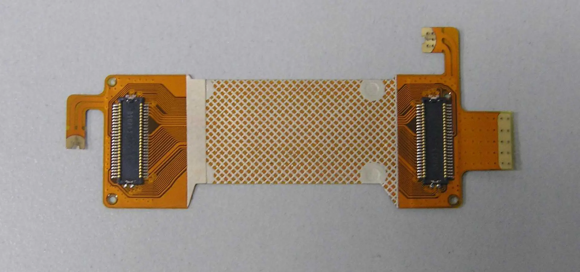
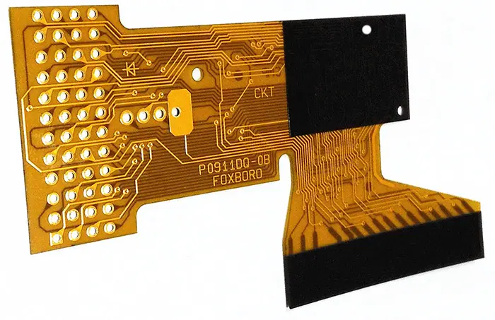
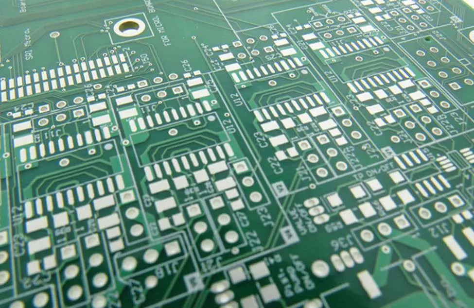
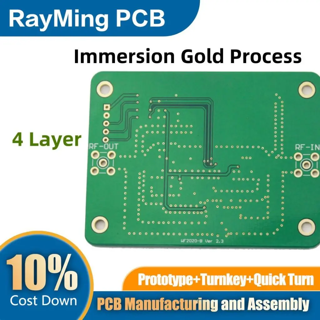
Correct PCB pad design is crucial to effectively weld components to the circuit board. For bare pad  prototype pcb assembly , there are two common welding methods โ€” SMD (Solder Mask Defined) and NSMD (Non-Solder Mask Defined), each with its own characteristics and advantages.

The Difference Between SMD and NSMD

SMD:

SMD refers to the resistance layer opening is less than the metal pad welding process. This process reduces the possibility of the welding plate falling off during welding or dewelding. However, the disadvantage is that the method reduces the copper surface area that can be used for solder joint connections and reduces the space between adjacent pads. This limits the thickness of the trace lines between the pads and may affect the use of through-hole.

NSMD:

NSMD refers to the welding plate process in which the opening of the resistance layer is larger than that of the welding plate. This process provides greater surface area for solder joint connections and greater clearance between solder pads (compared to SMD), allows for wider line width and more through-hole flexibility, but NSMD pads are more likely to fall off during welding and disassembly. Even so, NSMD still has a better welding firm performance and is suitable for solder joint sealing pads.

Introduction

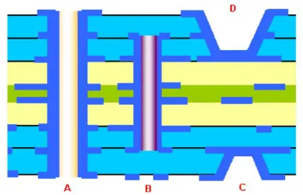
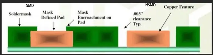
Ball grid array (BGA) packages are widely used for integrated circuits as they provide a high density of interconnections beneath the package. BGA packages connect to the PCB through an array of solder balls that serve as the leads. When defining the PCB land patterns or footprint for the BGA package, the solder mask design requires special consideration for reliability. The solder mask can either cover the copper pad completely, known as solder mask defined (SMD), or have openings larger than the pad diameter, called non-solder mask defined (NSMD).

This article explains what SMD and NSMD BGA footprints are, their differences, key design considerations, assembly process impacts and applications.

Solder Mask Defined (SMD) BGA Footprints

YouTube video

In an SMD BGA footprint, the openings in the solder mask layer fully cover and intersect the underlying copper pads. This results in the solder mask itself defining the final land dimensions and controlling the volume of solder paste printed. Hence the name solder mask defined (SMD) footprint.

With SMD footprint, the copper pad size is typically 20 to 60 ฮผm greater than the solder mask opening based on registration tolerances. The key characteristics of SMD BGA land patterns are:

  • Solder mask opening equals the intended land diameter for the BGA balls. This controls the amount of solder.
  • Excellent registration is needed between layers to keep the pad centered in the mask opening.
  • The pad shape is not critical and there is no risk of exposed copper.
  • Allows smaller pad and pitch dimensions since solder mask dams prevent bridge formation.
  • Solder voiding can occur more easily due to smaller paste volumes.

Here is an illustration of solder mask defined (SMD) BGA footprint:

The tight alignment between copper pad and solder mask opening required for SMD footprint necessitates use of the tightest manufacturing tolerances.

Non-Solder Mask Defined (NSMD) BGA Footprints

In a non-solder mask defined (NSMD) footprint, the openings in the solder mask layer are larger than the diameter of the copper pads. This exposes the entire copper pad allowing the pad size and shape to define the final land dimensions rather than the solder mask.

In NSMD footprint, the mask openings exceed the copper pad size by at least 150 ฮผm based on registration tolerances. Key features are:

  • The pad diameter determines the solder volume. Solder mask does not restrict soldering.
  • Requires greater clearance between pads to prevent mask bridging since mask does not dam solder flow.
  • Copper pad can be dog-bone or dumbbell shaped to allow solder filleting.
  • Pad registration to mask opening is non-critical. Mask just needs to expose pad.
  • Allows larger paste deposit area so less prone to solder voids.

Here is an illustration of non-solder mask defined (NSMD) footprint:

The NSMD design provides more tolerance for pad positioning within the mask opening but demands greater spacing between adjacent pads.

Comparison Between SMD and NSMD Footprints

Here is a summary comparison of some key differences between the solder mask defined (SMD) and non-solder mask defined (NSMD) footprints for BGA packages:

ParameterSMD FootprintNSMD Footprint
Mask opening vs. padEqual to pad diameterAt least 150 ฮผm greater than pad
Solder volume controlDefined by mask openingDefined by pad diameter
Pad shapeLimited by mask openingCan use dogbone, dumbbell shapes
bridging riskLower – mask dams prevent solder spreadHigher – no mask dams so needs more spacing
Registration needsTight mask to pad registration essentialPad registration non-critical
Solder voidingHigher risk due to small volumesLower risk thanks to larger paste deposits
Design and assembly costGenerally higherLower cost

In summary, SMD design works best for fine pitch parts where the solder mask yields precise solder volumes, while NSMD is preferable for larger packages needing greater process and registration tolerances.

SMD Footprint Design Guidelines

When designing an SMD footprint for a BGA package, here are some guidelines to follow:

  • Pad diameter should be 20 to 60 ฮผm less than mask opening based on registration capabilities
  • A minimum web of 50 to 75 ฮผm is required between adjacent mask openings
  • Laser cut mechanically drilled (LCMD) vias can be placed within pad area if space is tight
  • 1:1 pad to ball ratio should be used for perimeter balls
  • Non-perimeter pads can utilize area array patterns to increase routing space
  • Pad shapes are largely non-critical since mask controls shape and volume
  • Thermal reliefs in pad are not beneficial due to small paste volumes
  • For dense footprint, use tighter mask to pad tolerances for web reduction
  • Reduce pad spacing further by shifting adjacent rows/columns by 50% pitch
  • Use thicker mask of at least 150 ฮผm to prevent tacky solder damage

NSMD Footprint Design Guidelines

For non-solder mask defined BGA footprints, following guidelines are recommended:

  • Pad diameter should be smaller than mask opening by at least 150 ฮผm
  • Minimum web of 225 ฮผm should be kept between mask openings
  • Dogbone, dumbbell pad shapes can be used to improve solder filleting
  • LCMD vias must be placed clear of extended pad edges
  • 1:1 pad assignment preferred on package perimeter
  • Thermal reliefs can be incorporated in pad shapes
  • Increased spacing required between pads due to lack of solder dams
  • Thinner solder mask down to 75 ฮผm can suffice if bridging risks are low
  • Tighter mask to pad registration not needed allowing faster assembly
  • Can shift adjacent rows/columns by 25% pitch only due to bridging risks
  • Suitable for footprint sizes above 15mm ร— 15mm

Assembly Process Impacts

The choice between SMD or NSMD footprints for a BGA package influences various aspects of the assembly process:

Stencil Design

For SMD pads, stencil openings equal the pad size as mask defines shape. For NSMD pads, stencil openings must be smaller than pad area to control solder volume.

Solder Paste Printing

NSMD pads allow larger print deposits reducing voids. SMD pads need tighter print process control to prevent solder balls.

Pad Tolerance Changes

SMD needs tight mask to pad registration. NSMD relaxes this requirement allowing cheaper PCB fabrication.

Spacing and Routing

NSMD needs more clearance between pads forcing larger pitch. This consumes more PCB area but eases routing.

Voiding Risks

The smaller paste deposits of SMD make it more prone to voids versus NSMD pads.

Bridging Risks

Lack of mask dams means NSMD has higher bridging risks requiring careful paste volume control.

Fillet Formation

NSMD allows pad shapes to improve solder side filleting. SMD shape is restricted by mask aperture.

Rework Concerns

SMD pads limit where heat can be applied during rework. Mask restricts access to NSMD pads less.

SMD vs NSMD Applications

SMD footprints are preferred for:

  • Fine pitch BGA packages โ‰ค 0.8mm pitch
  • Small BGAs with pitch โ‰ค 0.5mm
  • Packages with high pin counts
  • Portable consumer electronics where space is critical

NSMD footprints suit:

  • Lower density BGA packages with >1mm pitch
  • Larger package sizes above 15mm x 15mm
  • Automotive grade parts needing greater process tolerances
  • Corner ball cases requiring dogbone pads for sufficient solder volume
  • Boards with fewer routing layers where pad spacing is less critical
  • Applications where solder voiding risks need minimization

Summary

In summary, solder mask defined (SMD) BGA footprints provide precision solder control by limiting paste volumes but demand tight fabrication tolerances. Non-solder mask defined (NSMD) pads relax tolerances but occupy more space on the PCB unless carefully designed. Making the right choice based on pitch, pad count, size constraints and process capabilities is key to designing a reliable and manufacturable BGA footprint.

FAQs

Can SMD or NSMD be used for any BGA pitch?

SMD is preferred for fine pitch below 0.65mm due to solder control. NSMD is unsuitable below 0.5mm because of bridging risks from lack of dams.

Which provides better resistance to shock and vibration?

NSMD allows larger fillets so can withstand mechanical stresses better. SMD may crack more easily at the package edges and corners.

Is NSMD also called extended pad in some datasheets?

Yes, extended pad is another term used to indicate NSMD footprint where pad extends beyond the solder mask opening.

Does NSMD increase the risk of thermomechanical fatigue?

Slightly – the larger pad size leads to higher shear stresses at the pad periphery which must be considered in reliability testing.

Can thermal vias be incorporated in BGA pads?

For SMD pads thermal vias will reduce solder volume further increasing void risks. In NSMD thermal vias can be safely placed provided they do not infringe on the extended pad area.

What is the Stiffener for FPC?

pcb board stiffeners

Introduction

Flexible printed circuits (FPCs) are widely used to interconnect components in products like mobile phones, wearables, displays, medical devices etc. where flexibility is required. FPCs use thin and flexible polymer materials as the base substrate unlike rigid printed circuit boards (PCBs). However, this flexibility also makes FPCs prone to bending and twisting stresses during handling, assembly and use. Stiffeners can be attached to FPCs to provide localized reinforcement and protect certain areas from these stresses.

This article will provide a detailed overview of FPC stiffeners – their role, materials used, design considerations, attachment methods and applications.

What is a FPC Stiffener?

An FPC stiffener is a relatively thick, rigid structure that is fixed to the FPC using adhesives at strategic locations. It helps prevent excessive flexing, twisting or bending of the FPC in those areas during manufacturing, assembly and usage. Stiffeners protect delicate components as well as the FPC substrate itself from damage due to handling and mechanical stresses. They also provide stiffness for connectors and interface points to external devices.

FPC stiffeners are commonly made using materials like stainless steel, FR4, polyimide and acrylics. Adhesives such as epoxies and acrylics are used to bond the stiffener securely to the FPC. The stiffener often includes holes and cutouts to allow mounting of ICs, connectors, buttons and other components.

Need for Stiffeners in FPCs

the flexible board requires a stiffener to obtain external support

While the thin, flexible construction of FPCs is advantageous for many applications, it also creates some unique challenges which FPC stiffeners help overcome:

  • The thin polyimide substrate can get damaged by repeated flexing and twisting stresses during assembly and usage. Stiffeners reinforce areas prone to such stresses.
  • Components on FPCs are also susceptible to failures and cracked joints due to excessive vibration or shock loads without support. Stiffeners protect fragile components.
  • Flexible sections of FPCs by nature are prone to frequent handling and manipulation during fabrication, component placement and testing. Stiffeners prevent damage to copper traces and joints.
  • Display driver ICs are sensitive to bending stresses due to the brittle silicon. Stiffeners support these components on display driver FPCs.
  • Connectors and interface points to other PCBs or cables undergo mechanical stresses which can crack solder joints. Stiffeners prevent flexing damage.
  • Stiffness is required during handling, clamping and assembly of FPCs using automatic equipment. Targeted stiffeners facilitate this.
  • Stiffened areas can be grabbed or held firmly during manual assembly and repair procedures without causing damage due to bending.
  • Components mounted on stiffened islands remain stable for inspection and rework. Flexible FPCs can distort from flatness.
  • Stiffeners allow mounting of components on both sides of FPCs without short circuits due to touch. Open areas can be kept flexible.

FPC Stiffener Materials

Stiffeners designed for FPCs need to meet requirements like dimensional stability, mechanical stiffness, easy machinability or stamping, moisture resistance and adhesion compatibility with the FPC substrate and components. Here are some common materials used:

Plastics

Polyimide sheets offer a balance of stiffness, temperature resistance, dimensional stability and cost-effectiveness. Popular grades include Vespel, Duratron and Kapton. However, polyimide absorbs some moisture which may be unsuitable for high humidity environments. It has limited chemical resistance against solvents.

Acrylics like PMMA provide good moisture and chemical resistance along with stiffness and stability. PMMA stiffeners retain flexibility and do not become brittle over time. They adhere well to FPC substrates using acrylic adhesives. However, acrylics have relatively lower temperature ratings.

Polycarbonate offers high tensile strength for mechanical rigidity combined with temperature resistance exceeding 155ยฐC. It also offers flame retardant properties required in some applications. Polycarbonate is prone to environmental stress cracking however.

LCP (liquid crystal polymer) grades like Zenite offer the best temperature resistance (>240ยฐC) and stiffness among plastic options. LCP has excellent chemical resistance and ultra-low moisture absorption. But it is an expensive material choice.

Metals

Stainless steel offers extremely high stiffness and environmental resistance. It can withstand repeated flexing without cracking. Steel can be easily stamped or machined to desired shapes. It needs nickel/gold plating for soldering compatibility. Stainless steel substantially increases the weight of the FPC assembly.

Aluminum provides good stiffness-to-weight ratio and corrosion resistance while being lighter than steel. It is also low cost and easy to fabricate, but not as rigid as steel for the same thickness. Plating may be needed for soldering.

Copper has excellent thermal conductivity to dissipate heat from components. This lightweight metal stiffener can be readily soldered to the FPC copper traces without plating. But copper is prone to corrosion and needs protective coatings.

Kovar alloy has matching coefficient of thermal expansion (CTE) as silicon chips, minimizing solder joint stresses. However, kovar is not easily soldered and is mainly used as leadframes for ICs rather than stiffeners.

Brass offers good stiffness and manufacturability though not as strong as steel. It is prone to corrosion and needs protective nickel-tin plating typically. Soldering compatibility is also excellent.

Composites

FR-4 combines good stiffness, dimensional stability and cost-effectiveness. It can withstand processing temperatures over 150ยฐC. Being fiberglass reinforced epoxy, it bonds well with the FPC substrate. However, FR-4 absorbs moisture and is not suitable for all environments.

CEM-1 laminates consisting of woven glass fabric in a cyanate ester resin provide the highest thermal capabilities as stiffeners, withstanding over 280oC. They have very low outgassing and moisture absorption. But CEM-1 material cost is also high.

Carbon fiber composites offer extremely high rigidity for their weight, along with corrosion resistance and ambient temperature tolerance exceeding 200ยฐC. The high cost of carbon fiber is the main deterrent.

FPC Stiffener Design Considerations

Some key factors to consider during design of FPC stiffeners are:

Stiffness requirements – The amount of flex that needs to be prevented guides required stiffness. This helps select the material and thickness.

Area coverage – Partial patches or strips may suffice for localized reinforcement versus covering larger areas. Stiffener footprint impacts weight, cost and assembly considerations.

Component space – Cutouts, holes or voids need accommodation in the stiffener for mounting components, connectors, displays etc.

Routing provisions – Stiffener location should avoid blocking interconnection paths between components located on both sides of the FPC.

FPC material and layers – More layers and thicker dielectric require higher rigidity for equivalent stiffening. Stiffener adhesive selections depend on the FPC substrate.

Assembly and inspection – Stiffener should not hamper component placement, clamping, machine handling or manual assembly. Visual inspections and rework access need consideration.

Weight and thickness – Overall thickness after stiffener installation should meet product specifications. Weight limits steer material selection for wearable and portable devices.

Environment – Temperature range, chemical exposure, moisture levels and outgassing drive stiffener material selection.

Thermal dissipationHeat dissipation may require thermally conductive stiffeners under high power components. Electrical and thermal insulation is needed for some applications.

Reworkability – Strippable stiffener adhesives may be preferred to allow rework of underlying components after stiffener attachment.

FPC Stiffener Attachment Methods

The stiffener must be securely fixed to the FPC substrate to prevent separation or movement during use. The common joining methods include:

Adhesive bonding – Acrylic, epoxy or polyimide adhesives are commonly used to bond the stiffener. Adhesive selection depends on materials and environmental needs. Die-cutting can create custom bondline shapes.

Soldering – For metal stiffeners, solder paste can attach and electrically ground it. Reflow attaches stiffener but risks heat damage to FPC substrate. Selective hand soldering is preferred.

Press-in – Interlocking press-fit features on metal stiffeners physically lock into the FPC substrate when compressed together. No adhesives are needed. Allows stiffener removal for repairs.

Clips – Metal spring clips or fasteners screwed into the stiffener mechanically clamp it to the FPC substrate firmly. Allows easy installation and removal.

Screws – Screws passing through clearance holes in the FPC substrate can thread into tapped holes in the stiffener to clamp it together. Supports reworkability.

Riveting – Rivets installed in the stiffener are peened over onto the FPC substrate to capture it. Allows stiffener removal by drilling out rivets.

Typical Applications of FPC Stiffeners

Some common applications where FPC stiffeners provide important benefits include:

Display driver FPCs – Stiffeners reinforce areas under driver ICs and connectors to prevent damage due to handling and vibration in devices like mobile phones, tablets, televisions etc.

Battery FPC interconnects – Mechanical robustness to withstand vibration and shocks over long device lifetimes make stiffeners essential for battery connector FPCs.

Medical products – For patient monitoring patches, implants and wearable devices, stiffeners allow robust interface connectors while keeping sensors flexible.

Automotive FPCs – Stiffeners used in cabling and sensors prevent damage due to continuous vibration and thermal cycles over vehicle lifetime.

Robotics – Frequent robotic arm and gripper movements require local stiffening on flex cables interconnecting movable sections for extended mechanical endurance.

Consumer Electronics – Stiffeners reinforce FPC connections to PCBs in smartphones, laptops and portable electronics that undergo drops and shocks.

Industrial – FPCs used in motion control systems, pneumatic valves, instrumentation etc. use stiffeners to create stable component mounting interfaces and robust cabling.

Benefits of FPC Stiffeners

Some key benefits provided by FPC stiffeners include:

  • Reinforce connector areas for increased mechanical robustness and reliability
  • Support fragile components like driver ICs and prevent failures
  • Allow clamping and assembly handling of FPC without damage
  • Improve stability for component placement, inspection and rework
  • Prevent copper trace damage due to repeated bending stresses
  • Absorb vibration and shock loads instead of transmitting them to FPC
  • Facilitate manual and automated assembly and fabrication processes
  • Allow double-sided component mounting for increased density without shorts
  • Enable reliable performance over expected product lifetime
  • Protect flexible cable segments from complex motion stresses

FAQs

Do FPC stiffeners help in heat dissipation?

Yes, choosing a thermally conductive stiffener under high power components allows heat spreading into the stiffener effectively. This reduces local hot spots.

Can multiple small stiffeners be used instead of one large one?

Yes, multiple discrete stiffener patches can be used for localized reinforcement and component protection instead of a single large stiffener.

Is the stiffener always in direct contact with FPC substrate?

Not always – standoffs can create an airgap between stiffener and FPC to facilitate inspection while still providing mechanical protection.

What tolerance is essential in FPC stiffener fabrication?

As stiffeners align FPC substrates for assembly, typical machining tolerance held is around ยฑ0.10 mm. For placement near connectors or components, ยฑ0.05mm tolerance or better is recommended.

How thick is a typical FPC stiffener?

Stiffener thickness depends on rigidity required but is typically in 0.3mm to 1mm range. Stainless steel can be as thin as 0.1mm but plastics need to be thicker for equivalent strength.

The importance of FPC stiffener

The Flex PCB stiffener refers to a stiffener attached to the back of the FPC when a widget such as a connector is attached to the FPC.

FPC stiffener
fr4 stiffener

From the point of view of reinforcing materials, various materials, including metals and resins, can be provided depending on the application.

pi stiffener material

FPC๏ผˆFlexible Printed Circuit๏ผ‰it is a soft and flexible structure. This is the biggest feature of FPC, but due to its soft structure, when connecting a small part such as a connector to an FPC, it is necessary to place a reinforcing plate on the back side of the electronic component to which the connector is attached.

But why do you want to put a stiffener? There are three main reasons for this. 1 solder resist off measure 2 solder pad drop countermeasure As shown in the right side of Figure 1, when the connector mounted on the FPC is inserted and removed, the FPC is soft, so external force is applied to the terminal portions of some connectors. As a result, the welded portion may fall off directly. Similarly, since the copper foil portion (pad) of the FPC may also easily fall off from the underlying structure, the base portion. This is where the mat falls off.

In either case, as shown in the left part of Fig. 1, as long as a sufficiently stiff reinforcing plate is placed on the FPC, it is possible to prevent the force from being concentrated on the terminal portion, and the solder/pad can effectively prevent the falling off.

FLex PCB PI

3 Anti-substrate warpage countermeasures during reflow soldering

If the reinforcing plate is not attached during reflow soldering, the FPC will bend and the correct soldering may not be possible.

At the same time, even if it is difficult to weld, the mounting portion sometimes bends, which causes the mounting failure. (parts fall off)

In order to keep the mounting surface flat and securely mounted, the reinforcing plate is essential.

FLEX PCB SMT PI

What is High Density PCB?

High-Speed High-Density PCB

Introduction

Printed circuit boards (PCBs) form the backbone of all electronic devices providing the platform to mount components and interconnect them. With rapid technological advancements and need for product miniaturization, PCBs have become increasingly complex and crowded. This had led to the growth of high density interconnect (HDI) PCB technology to provide the wiring density needed by advanced electronics.

High density PCBs allow packing of high component densities and fine features into smaller board areas. They enable integration of more functionality into compact and lightweight electronics. HDI capabilities are critical for products like smartphones, wearables, IoT devices, medical equipment etc. that require maximum hardware capabilities within tight space constraints.

This article will provide an in-depth understanding of what constitutes a high density PCB, the key technologies enabling HDI boards and their applications.

What Makes a PCB High Density?

qrf

A high density PCB can be defined as a board with:

  • Fine trace/space width โ‰ค 100 ฮผm (4 mils)
  • High layer count โ‰ฅ 6 layers
  • Blind and buried vias for routing between inner layers
  • Microvias with diameters โ‰ค 150 ฮผm, typically 50 to 80 ฮผm
  • High component density with pad/pitch โ‰ค 0.4 mm

To achieve these high wiring densities, HDI PCBs leverage technologies like laser drilling and imaging of fine features, thinner dielectrics, sequential lamination, and more.

Some key characteristics of HDI boards from standard PCBs are:

FeatureStandard PCBHDI PCB
Line/Spaceโ‰ฅ 125 ฮผmโ‰ค 100 ฮผm
Via diameterโ‰ฅ 150 ฮผmโ‰ค 80 ฮผm
Via pad sizeโ‰ฅ 350 ฮผmโ‰ค 250 ฮผm
Layer countโ‰ค 12โ‰ฅ 6, up to 30+
Dielectric thicknessโ‰ฅ 50 ฮผmโ‰ค 40 ฮผm
Solder maskLiquid photoimageableLaser direct imaging
Finished thicknessโ‰ฅ 1.6 mmโ‰ค 1.0 mm

Evolution of High Density Interconnect Technology

The origins of HDI technology can be traced back to the 1980s when traditional PCB fabrication techniques started reaching their limits as circuit densities grew. Some key milestones in the development of HDI are:

  • Mid 1980s – Surface mount technology and multilayer boards started gaining adoption to support denser packaging and routing.
  • Late 1980s – Microvia technology was developed by IBM allowing connections between layers with small vias. This avoided the need to route lines all the way to the outer layers.
  • Early 1990s – Build up layer (BUL) process introduced by Intel-Microsoft consortium to build additional thin signal layers on top of a core board.
  • Mid 1990s – Laser direct imaging adopted for fine photolithography to create traces below 25 ฮผm.
  • Early 2000s – Stacked microvias and sequential lamination refined the basic HDI processes.
  • 2010s – With growth of smartphones, HDI became ubiquitous globally. Lines/spaces dropped below 20 ฮผm.

Continued innovation in materials and processes has enhanced the capabilities of HDI technology to keep pace with market requirements.

Key Technologies Enabling High Density PCBs

A number of advanced PCB fabrication technologies are essential to manufacture the high density boards needed today:

Laser Drilling

Mechanical drilling cannot achieve the 5 mil and lower via sizes seen in HDI. UV lasers are used drill these miniscule vias with high accuracy at tight pitches. Laser also produces cleaner via walls and avoids issues like smear and epoxy clogging faced with small bits.

Thin Dielectrics

Standard glass fabric substrates are too lossy and thick for high speed HDI boards. Teijinโ€™s Nexus and Panasonicโ€™s Megtron 6 are popular low-loss thermoset laminates with dielectric thicknesses down to 25 ฮผm. These allow tighter lines/spaces and prevent signal integrity issues.

Direct Imaging

To fabricate ultra-fine traces below 25 microns, photolithographic methods are used instead of mechanical print-and-etch process. Liquid photoresists are exposed using laser direct imaging to define the circuit patterns with high precision.

Blind and Buried Vias

Blind/buried vias are drilled and plated before lamination of the outer layers, allowing connections between inner layers without consuming routing space. This provides tremendous routing flexibility in HDI designs.

Microvias

These are small vias with diameters typically between 50 to 80 ฮผm drilled with lasers. Microvias connect adjacent layers in HDI boards without using board area.

Build Up Layers

Additional thin dielectric layers are added on either side of the core HDI board using sequential lamination. These provide more routing layers to relieve congestion and integrate components.

Fine Pad/Pitch SMT

To place more components in smaller areas, fine pitch component packaging from 0.4 to 0.15mm pitch is used. The PCB fabrication process must achieve the pad geometries and tolerances needed for this.

HDI Board Construction

HDI PCB Board Laminate Structure-PCB Manufacturer-4

There are three fundamental types of HDI board constructions used:

1. Basic HDI

This construction has 4 to 8 blind via layers with at least one fine line top or bottom layer joined by microvias. Blind vias route between internal layers eliminating the need for via stubs. A 25 to 50 ฮผm finish layer can integrate fine pitch SMT components.

2. Complex HDI

Complex HDI boards sandwich very thin core and buildup layers containing microvias between thicker sub-assemblies containing conventional and blind/buried vias for routing density. There can be multiple such sub-assemblies in large boards.

3. Sequential Lamination HDI

Here the core board contains 6 to 12 layers. Then additional build up layers are added sequentially by laminating 25 to 60 ฮผm thin dielectric films. Vias in each layer are stacked to form connections between the layers. Components can be embedded in the outer build up layers.

The choice of HDI construction depends on layer count, component density, routing congestion and other design needs.

Applications of High Density PCBs

Some major application areas where HDI PCB technology provides major benefits are:

Consumer Electronics

Smartphones, tablets, wearables and other compact consumer electronic devices extensively use HDI boards to cram maximum functionality into limited space. The small via sizes help in routing dense chip-scale packages (CSP).

Automotive Electronics

Infotainment systems, advanced driver assistance systems (ADAS) and vehicle control units need HDI boards due to high component densities. Weight and fuel efficiency demands also drive adoption.

Medical Electronics

Medical equipment like imaging systems, patient monitors etc. require HDI PCBs to integrate multi-modality functionality into small, ergonomic and portable devices.

Aerospace and Defense

Avionics, radar and electronic warfare systems use rugged, lightweight HDI boards with high layer counts for excellent signal integrity and noise control in harsh environments.

High-End Computing

Supercomputers, data servers and network switches demand maximum speeds which is enabled by HDI PCBs due to their electrical performance advantages.

Advantages of Using High Density PCBs

Some benefits offered by high density PCBs are:

  • Space saving – HDI technology provides 2-4x improvement in component packaging density versus conventional PCBs. This enables product miniaturization.
  • Design flexibility – The routing flexibility offered by microvias and additional routing layers accommodates last-minute design changes easily.
  • Signal integrity – Electrical performance is improved by allowing shorter traces, matched lengths, tighter layouts and fewer stubs/vias.
  • Lower costs – Despite higher initial cost, fewer PCBs are needed so system cost reduces. Overall manufacturing costs also lower due to tiny components.
  • Weight reduction – Elimination of wires and backplanes along with smaller components reduces weight significantly for aerospace and portable applications.

Challenges in High Density PCBs

Some key challenges faced in designing and manufacturing HDI boards are:

  • Extremely tight tolerances in fabrication require advanced processes and equipment. This increases cost.
  • Thermal management is difficult due to high power densities. This requires planning for heat sinks, thermal vias etc.
  • High costs of rework due to microvia holes makes designs unforgiving of mistakes.
  • Signal and power integrity demands complex analysis and modeling to prevent issues.
  • Warpage due to coefficient of thermal expansion (CTE) mismatches in thin multilayers requires careful material selection.

Future Outlook

Emerging applications like Internet of Things (IoT), wearables, electric vehicles etc. will drive greater adoption of HDI technology. Additive manufacturing and substrate-like PCBs will enable embedding of components. Line widths may shrink below 10 ฮผm driven by 5G rollouts. However, fabrication costs and margins will remain challenges for further innovations.

FAQs

What is the key difference between conventional PCB and HDI PCB?

The ability to fabricate fine features like traces below 100 ฮผm and microvias below 150 ฮผm sets HDI boards apart. This provides much higher wiring densities.

Is HDI PCB suitable for analog circuits?

Not usually – the high frequencies and close coupling in HDI boards increases noise pickup and crosstalk. Standard PCBs are generally preferred for analog/mixed signal designs.

Can components be embedded inside HDI PCB?

Yes, additional build up layers can be used to create cavities for embedding bare die, capacitors, resistors etc. This helps further reduce size and enhances electrical performance.

Are HDI PCBs prone to failure due to thinner dielectrics?

With careful handling and component selection, reliability is not compromised. The adhesion between dielectric films is critical however and tested thoroughly during qualification.

How are very small microvias in HDI boards plated?

Specialized techniques like panel plating using a conformal anode are used to achieve uniform plating and void-free copper filling of high aspect ratio microvias.

4 Tips in high-speed (>100MHz) high-density PCB design

In the case of fixed circuit board size, if more functions need to be accommodated in the design, it is often necessary to increase the track density of the PCB, but this may cause mutual interference of the track to be enhanced, and the track are too thin to make the impedance impossible to reduce. . Pay attention to crosstalk interference when designing high-speed, high-density PCB because it has a large impact on timing and signal integrity. Here are a few caveats:

1. Control the continuity and matching of the trace characteristic impedance.

2. The trace space. The spacing commonly seen is twice the line width. The simulation can be used to know the influence of the trace spacing on timing and signal integrity, and to find the minimum space that can be tolerated. The results may vary from analog chip to chip. Choose the appropriate termination method. Avoid the same running direction of the upper and lower adjacent layers, or even overlap with each other because the crosstalk is larger than that of the adjacent lines in the same layer.

rf pcb design

3. Use blind/buried via to increase the area of the track. However, the manufacturing cost of the PCB board will increase. It is really difficult to achieve full parallelism and equal length in actual implementation, but still try to do it.

high speed pcb design tutorial

4. Differential termination and common-mode termination can be reserved to mitigate the effects on timing and signal integrity.

What are the different surface finishes in PCB?

pcb surface finish

Introduction

Printed circuit boards (PCBs) form the backbone of all electronic devices. They provide the mechanical support structure to mount various electronic components and interconnect them through conductive copper tracks to form functioning circuits. The copper tracks and pads on the PCB that connect the various components need to be protected from oxidation and corrosion to maintain the electrical conductivity and solderability. This is achieved by applying different types of surface finishes over the exposed copper on the PCB.

There are various types of surface finishes available for PCBs, each with their own sets of pros and cons. Selecting the right surface finish for a PCB design requires carefully weighing factors like cost, solderability, oxidation resistance, contact resistance, assembly process compatibility, reworkability and more. The most common finishes used in PCB fabrication today include:

  • Hot Air Solder Leveling (HASL)
  • Immersion Silver (IAg)
  • Immersion Tin (ISn)
  • Electroless Nickel Immersion Gold (ENIG)
  • Organic Solderability Preservatives (OSP)
  • Electroless Nickel Electroless Palladium Immersion Gold (ENEPIG)

This article provides a detailed overview of these popular PCB surface finishes, their characteristics, typical applications and process methods used to apply them.

PCB Surface Finishing Processes

PCB Immersion Gold vs PCB Gold Plating

Surface finishing of PCBs is typically done after the boards have gone through the complete fabrication process of lamination, drilling, metallization and imaging. The exposed copper tracks are coated with the selected surface finish to protect the copper from oxidation and maintain solderability. There are various techniques used for depositing the different finish layers:

Electroplating

This involves submerging the PCB in a electrolytic bath containing the coating metal ions (tin, silver, gold etc.) and applying electric current to facilitate deposition of the metal layer onto the copper through reduction reactions. Electroplating allows deposition of uniform, smooth and shiny metallic coatings.

Electroless Plating

In this process, the PCB is dipped in a aqueous solution containing the plating metal (nickel, gold, palladium etc.) and a reducing agent. The reducing agent reacts with the metal ions leading to autocatalytic deposition of the metal layer onto the copper surface without external current.

Hot Air Solder Leveling

In this technique, the PCB is passed over a molten solder wave. The solder adheres to the copper tracks forming a coating. Hot air knives immediately blow hot air to flatten out the solder layer and give a smooth finish.

Organic Surface Preservatives

The PCB is dipped in an organic solution containing additives like imidazole, benzimidazole etc. which form an invisible thin coating and prevent copper oxidation.

With this background on the commonly used PCB surface finishing processes, let us now look at the popular finishes in more detail.

Hot Air Solder Leveling (HASL)

Hot air solder leveling using tin-lead alloy was the most prevalent PCB finish for many decades due to its low cost, ease of application, repairability and acceptable performance. However, due to the toxicity of lead and subsequent ban on lead usage in electronic assembly, lead-free solders have become standard for HASL finish.

Composition

The HASL finish consists of a thin layer of solder alloy coated over the copper conductors on the PCB. Common solder alloys used are:

  • Sn96.5/Ag3/Cu0.5 (SAC305) – Melting point 217??C
  • Sn95.5/Ag3.8/Cu0.7 (SAC387) – Melting point 219??C
  • Sn99.3/Cu0.7 (SAC0307) – Melting point 227??C

These lead-free solders provide comparable performance to tin-lead solders. The thickness of the finish typically ranges from 1 to 3 mils.

Process

The steps in the HASL process are:

  1. Flux application – The PCB goes through a foam fluxer unit containing flux solution to clean the copper and prepare it for soldering.
  2. Preheating – The board is preheated to about 150??C to evaporate solvents in the flux and activate it.
  3. Solder coating – The hot PCB (typical solder bath temperature 240-260??C) passes over a pumped solder wave which deposits and evenly coats the molten solder over the entire board surface.
  4. Hot air leveling – High pressure hot air knives (245-255??C) immediately blow down on the solder coated board. This flattens out the solder, removing any peaks and valleys, giving an even, smooth finish.
  5. Cooling and cleaning – The board cools down as it exits the HASL system. Residual flux is washed off in a cleaning unit.

Advantages

  • Low cost process due to high throughput.
  • No special PCB fabrication processes required.
  • Provides good solderability. The solder finish itself acts as a permanent coating.
  • Easy rework of components by locally applying solder.
  • Repairable finish unlike ENIG, ISn etc. Damaged boards can be re-finished.

Disadvantages

  • Can cause unevenness on small component leads and test pins.
  • Flux residue entrapment can lead to corrosion and dendrite growth.
  • Thickness control harder versus plating processes.
  • Exposed finish prone to oxidation requiring nitrogen storage.
  • Thermal fatigue issues due to CTE mismatch with copper.
  • Unsuitable for fine pitch components due to bridging risk.
  • Lead contamination risk in solder bath affects long term reliability.

Applications

HASL continues to be used for cost-sensitive applications like:

It is often avoided for high reliability or fine pitch boards. The most common lead-free solder used is SAC305 which provides good solderability.

Immersion Silver (IAg)

immersion-silver-pcb

Immersion silver finish has emerged as a popular and cost-effective replacement to HASL for many applications. It avoids the unevenness and bridging issues faced with HASL for fine pitch ICs and offers better coplanarity. The immersion silver plating process is simple and does not need any special PCB fabrication adjustments.

Composition

The immersion silver deposit consists of pure silver. The plating thickness is typically 2 to 5 micro-inches (0.05 to 0.125 microns).

Process

Immersion silver plating involves the following steps:

  1. Surface preparation – The copper pads and traces are microetched to remove oxides and activate the surface.
  2. Silver deposition – The PCB is immersed in a silver plating solution containing a silver salt (typically silver nitrate) and a reducing agent. The reducing agent facilitates deposition of silver ions onto the copper surfaces.
  3. Rinsing and drying – The plated board is rinsed thoroughly in deionized water to remove any chemicals. It is then hot air dried.

The immersion silver process typically takes just 2-3 minutes and can easily be integrated into standard PCB fabrication lines.

Advantages

  • Provides excellent solderability comparable to HASL.
  • Uniform thickness deposition across pads, leads and test pins.
  • Solves issues of HASL like icicling, flagging and bridging.
  • Lower cost than other common finishes – ENIG, ENEPIG etc.
  • Suitable for fine pitch components.
  • RoHS compliant and halogen free process.

Disadvantages

  • Silver tarnishes and oxidizes over time which can degrade solderability. Shelf life is limited.
  • Not easily repairable unlike HASL. Damaged boards need to be re-plated.
  • Slightly higher cost compared to HASL process.
  • Does not prevent whisker growth like immersion tin.

Applications

The low cost, excellent solderability and fine pitch compatibility of immersion silver has made it the most widely used surface finish today for a range of applications:

  • Cellphones, tablets and portable electronics
  • Computer motherboards and graphic cards
  • Telecommunication hardware
  • Automotive electronics

It provides drop-in replacement capability for HASL. The limited shelf life means Ag plated boards are best assembled within 6-12 months.

Immersion Tin (ISn)

Immersion tin finish provides an economical way to protect copper traces from oxidation while retaining excellent solderability. The matte tin coating prevents whisker growth which has made it popular for high reliability applications.

Composition

The immersion tin deposit on PCBs consists of pure tin. The thickness typically ranges from 1 to 5 micro-inches (0.025 – 0.125 microns).

Process

The immersion tin plating process involves the following steps:

  1. Surface preparation – Microetching cleans the copper surfaces and activates them for plating.
  2. Tin deposition – The PCB is immersed in a heated tin salt solution containing a reducing agent. This causes deposition of Sn ions as a thin uniform metallic tin layer.
  3. Rinsing and drying – the plated board is thoroughly rinsed and then dried using hot air.

The immersion tin plating process adds minimal cost to PCB fabrication.

Advantages

  • Provides excellent solderability. Comparable to HASL for leaded and lead-free solders.
  • Lower cost compared to other platings – ENIG, ENEPIG.
  • Uniform thickness across component leads, test pads etc.
  • Matte grey finish prevents tin whisker growth risks.
  • Suitable even for ultra-fine pitch components.
  • Long shelf life with good oxidation resistance.

Disadvantages

  • Can have adhesion issues during thermal cycling leading to cracking.
  • Not easily repairable compared to HASL process.
  • Higher cost versus HASL process.
  • Dull cosmetic finish.

Applications

The whisker resistance, stable solderability and fine pitch compatibility of immersion tin make it well suited for high reliability applications:

  • Aerospace and defense electronics
  • High-end telecom, 5G and networking gear
  • Automotive electronics
  • Medical equipment
  • Industrial electronics

Its ability to prevent tin whiskering has led to the wide adoption of this finish in these segments.

Electroless Nickel Immersion Gold (ENIG)

The electroless nickel immersion gold (ENIG) finish provides an excellent combination of durability, solderability, bondability, conductivity and corrosion resistance. This had made it the finish of choice for high-reliability and high-performance electronics over the past several decades, despite its higher cost.

Composition

ENIG finish consists of a bottom layer of nickel-phosphorus alloy topped by a thin layer of immersion gold. Typical thickness is:

  • Electroless nickel: 80 to 250 micro-inches (2-6 microns)
  • Immersion gold: 3 to 15 micro-inches (0.08 – 0.4 microns)

Process

The ENIG process involves sequential plating of nickel and gold layers:

  1. Surface preparation – A microetch step removes oxides and activates the copper surface.
  2. Nickel plating – The PCB is immersed in an autocatalytic nickel bath where the exposed copper catalyzes deposition of nickel-phosphorus without any electrical current.
  3. Gold plating – The nickel layer is coated with a thin top layer of immersion gold by dipping in a gold plating bath containing a reducing agent.
  4. Rinsing and drying – Finally, the board is thoroughly rinsed in DI water and hot air dried.

Advantages

  • Provides excellent solderability combined with long shelf life.
  • Gold layer prevents copper/nickel oxidation.
  • Wear and abrasion resistant finish.
  • Uniform thickness deposition across component leads, test pads etc.
  • Good for both leaded & lead-free soldering.
  • Strong wire bondability.
  • Excellent corrosion and tarnish resistance.
  • Good electrical conductivity compared to other finishes.

Disadvantages

  • Relatively higher cost finish.
  • Not easily repairable or reworkable finish.
  • Nickel barrier prone to cracking under thermal fatigue.
  • Black pad risk due to thick nickel layer.

Applications

The superior reliability and performance characteristics have established ENIG as the finish of choice for critical applications:

  • High speed digital electronics – CPUs, GPUs, chipsets, memory
  • Aerospace and defense electronics
  • Telecommunication infrastructure
  • Automotive electronics
  • High-end consumer electronics

ENIG is also used where component wire bonding is needed. The thickness of the nickel layer is adjusted based on required corrosion resistance and current density.

Organic Solderability Preservatives (OSP)

osp pcb

Organic solderability preservatives provide an inexpensive way to protect copper traces from oxidation without the cost of metal plating. The organic coating prevents tarnishing while allowing soldering when needed.

Composition

OSP deposits consist of organic inhibitors like imidazoles, benzimidazoles, benzotriazoles etc. They form monolayers with a thickness of only a few molecules.

Process

The OSP application process is quick and involves:

  1. Surface preparation – The copper is microetched and activated prior to OSP deposition.
  2. OSP treatment – The PCB is immersed in a room temperature OSP solution containing organic inhibitors. These coat the copper surfaces.
  3. Rinsing and drying – Residual treatment solution is rinsed off, followed by drying.

The OSP process adds minimal fabrication cost and can easily be integrated.

Advantages

  • Extremely low cost compared to metal finishing.
  • Simple room temperature process.
  • Minimal effect on production process flow.
  • Provides temporary protection against oxidation.
  • Minimal risk of insertion issues versus thick metal layers.

Disadvantages

  • Shelf life limited to about 6 months.
  • Multiple heat cycles can degrade solderability.
  • Not suitable for high temperature or high reliability applications.
  • Repairing and reworking is difficult.
  • No wire bonding possible. Only for SMT parts.

Applications

The ultra-low cost of OSP makes it attractive for cost sensitive consumer electronic products with limited shelf lives:

  • Mobile phones
  • Tablets and laptops
  • IoT devices
  • Portable electronics
  • LED lighting

For long-life or high temperature products, other finishes like ENIG or Immersion Silver are used.

Electroless Nickel Electroless Palladium Immersion Gold (ENEPIG)

ENEPIG finish provides a cost-effective alternative to ENIG for many applications by replacing the immersion gold layer with electroless palladium + immersion gold. This reduces the overall gold consumption while providing excellent shelf life.

Composition

ENEPIG deposits consist of:

  • Electroless nickel: 2 to 5 microns
  • Electroless palladium: 0.05 – 0.3 microns
  • Immersion gold: 0.025 – 0.05 microns

Process

ENEPIG plating involves the following steps:

  1. Surface preparation using microetching
  2. Electroless nickel plating
  3. Electroless palladium plating
  4. Immersion gold – Double dip process
  5. Rinsing and drying

Advantages

  • Low gold consumption provides cost benefit over ENIG.
  • Shelf life, solderability and conductivity close to that of ENIG finish.
  • Good corrosion and oxidation resistance.
  • Palladium/Gold resists black pad risk.
  • Uniform deposition across component leads and pads.

Disadvantages

  • More expensive than tin, silver or OSP finishes.
  • Slightly lower bondability than with thick immersion gold.
  • Repair and rework is difficult.

Applications

The ENEPIG process allows reducing thickness (and cost) of gold layer without compromising shelf life or solderability. It is commonly used for:

  • High reliability telecommunications hardware
  • Aerospace and defense electronics
  • Automotive electronics
  • Medical electronics equipment
  • High-end industrial electronics

Faster depletion of thinner gold layer limits reworkability.

Summary of Common PCB Finishes

FinishTypical ThicknessProsConsApplications
HASL1-3 milsLow cost, repairable, good solderabilityThermal fatigue issues, uneven deposits, bridging risksCost-sensitive electronics
Immersion Silver0.05-0.125 ??mLow cost, excellent solderability, suitable for fine pitchOxidation and tarnishing issues, short shelf lifeCellphones, computers, telecom hardware
Immersion Tin0.025-0.125 ??mWhisker-free, excellent shelf life and solderabilityDull cos

How to know the surface finish from PCB color?

From the PCB surface, there are three main colors: gold, silver, and light red color. The PCB with gold color is the most expensive, the silver color is cheap, and the light red color is the cheapest.

You could know if the manufacturer have cut corners or not, from the surface color.

Besides, the circuit inside the board is mainly pure copper. The Copper is easily oxidized when exposed to air, so the outer layer must have the above protective cover.

  1. Gold color

Some people say that gold color is copper, that is not right.

Please refer to the picture with gold plating on the board as below:

immersion gold pcb board

The golden circuit board is the most expensive and is the real gold. Although it is thin, it also accounts for nearly 10% of the cost of the board.

There are two advantages for using gold, One is for welding conveniently and the other is for anti-corrosion.

As shown below, this is the golden finger of the memory stick 8 years ago. It is still golden and shining.

plated gold finger pcb

The gold-plated layer is widely used in circuit board component pads, gold fingers, connector shrapnel etc.

If you find that some boards are all silver, it must be cut corners. We call it โ€œcostdown.โ€

Generally speaking, the motherboards of mobile phone are gold-plated boards, but computer motherboards and small digital boards are not gold-plated.

Please refer to the board of iPhone X as below, The exposed parts are all gold plated.

gold plated pcb
  1. Silver color

Gold color is gold, silver color is silver? Of course not, it is tin.

immersion silver pcb board

The silver board is called a HASL board. Spraying tin on the outer layer of the copper, it also could help to welding, but it is not as stable as gold.

There is no effect on already welded components for HASL board. However, if pads are exposed to the air for a long time, such as ground pads and pin sockets etc, It is easy to oxidize and rust, resulting in poor contact.

All the small digital products are HASL boards. There is only one reason: cheap.

HASL PCB Board
  1. Light red color

OSP(Organic Solderability Preservatives), it is organic, not metal, So it is cheaper than the HASL process.

The only function of the organic membrane is to ensure the inner copper foil will not be oxidized before PCB soldering.

This membrane evaporates as soon as it is heated. Then you could solder the copper wire and components together.

But it is easy to be corroded. An OSP board canโ€™t be soldered if it is exposed to the air for more then 10 days.

There are many OSP processes in computer motherboards. Because the board size is too large.

osp pcb board

How to Detect Short Circuits in SMT Soldering

pcb short circuit

Short circuits are one of the most common defects in surface-mount PCB assembly using soldering processes like reflow soldering. They can lead to field failures and impair product function. Detecting shorts early using the right inspection methods is crucial for quality and reliability.

This article discusses ways to test for and identify different types of solder-related short circuits in SMT boards. It covers shorts between pads, traces, pins, component leads/terminations as well various inline and off-line electrical testing techniques with pros and cons. Recommendations are provided for choosing the optimal inspection strategy based on defect criticality, volume and cost considerations.

Introduction to Detection of SMT Shorts

A short circuit or โ€˜shortโ€™ is an unintended electrical connection between two conductors due to the following typical defects in SMT soldering:

Bridging – Solder forms a conductive bridge between adjacent pads, traces, component leads etc. which should be isolated.

Insufficient Clearance – Very close spacing of conductors allows conduction through residues or humidity.

Excess Solder – Extra solder creates shorting paths between neighboring conductors.

Tombstoning – Partially lifted SMD component creates short post-soldering between leads.

Solder Balls – Conductive solder spheres/splatter short adjacent exposed conductors.

Short circuits can cause:

  • Increased current draw damaging circuits.
  • Unwanted activation of components.
  • incorrect logic levels and erratic circuit behavior.
  • Intermittent contacts and reduced reliability over time.

Detecting and eliminating shorts in SMT assembly is thus critical for product function and robustness.

Test Methods for Detecting SMT Solder Shorts

YouTube video

Several testing approaches allow detecting solder shorts on surface mount boards:

Automatic Optical Inspection (AOI)

  • Captures images of post-soldering PCBs and analyses using algorithms.
  • Detects visible shorts like solder bridges.
  • Limited by resolution, optics and algorithm accuracy.
  • Typical in-line inspection technique.

X-Ray Inspection

  • Radiographic images reveal hidden shorts like insufficient clearance.
  • Requires expertise for analysis.
  • Used for inspection of critical components.
  • Time consuming for whole board inspection.

Flying Probe Testing

  • Electrically probes test nodes on powered-up board using flying probe heads.
  • Detects conductivity between shorted nets.
  • Limited access to nodes in dense boards.

ICT – In-Circuit Test

  • Tests board by probing test points at component pins level.
  • Detects shorts between component leads and nodes.
  • Fixtures limit access to dense boards.
  • Significant test development effort.

Boundary Scan Testing

  • Uses on-board JTAG circuitry for interconnect testing.
  • Detects short circuits between components with boundary scan cells.
  • Needs support from components.
  • Very thorough but system level focus.

Functional Testing

  • Validates board operation under simulation of actual conditions.
  • Behavioral anomalies reveal faults like short circuits.
  • System level focus. Software-based.

SMT Defects that Can Cause Short Circuits

Solder Bridging

  • Solder forms undesired bridge between traces or pads.
  • Caused by excess solder volume, improper temperature or component spacing.
  • Bridging across multiple pins of a component especially problematic.
  • Visual inspection or x-ray detects bridging. Electrical testing confirms.

Insufficient Clearance

  • Very narrow spacing between conductors.
  • Residues or condensation allows current flow under high humidity/voltage.
  • Caused by poor board design tolerances.
  • Detectable via x-ray or environmental stress screening.

Excess Solder

  • Extra unwanted solder creates shorting paths.
  • Due to issues in solder paste volume, reflow profile or component leveling.
  • Visual inspection reveals excess solder shorts.

Tombstoning

  • SMD components lift up on one side during reflow creating shorts between terminations.
  • Due to imbalanced wetting forces from poor paste stencil/volume.
  • Easily spotted under visual inspection.

Solder Balls/Splatter

  • Airborne solder particles solidify into conductive spheres.
  • Caused by solder slumping/splash during reflow.
  • Can short pads, traces positioned above solder joints.
  • Visual inspection identifies solder ball shorts.

Solutions for Preventing SMT Solder Shorts

SMT solder shorts can be minimized by:

  • Maintaining optimum soldering temperature, ramp rates and times.
  • Using no-clean, low residue flux to avoid bridging post-reflow.
  • Having adequate spacing between conductors based on voltage levels.
  • Containing solder paste volume between 0.66 to 1.5 times pad area.
  • Making stencil apertures inner dimensions match pad sizes.
  • Having sufficient clearance between stencil apertures to avoid solder bridging.
  • Using stencils of proper thickness – 0.1 to 0.15 mm typically.
  • Matching pad shapes/orientations to paste print direction to reduce tombstoning.
  • Making any board cutouts over 30 mm edge to edge to prevent solder balling.
  • Placing heat sinks and shields to avoid solder splash on areas prone to shorts.

Recommended Inspection Methods Based on Criticality

High Criticality – Full electrical testing – ICT, boundary scan combined with AOI and x-ray inspection. Ensures all shorts detected.

Medium Criticality – Sample electrical testing along with automated optical and x-ray inspection. Provides good defect coverage.

Low Criticality – Primarily automated optical inspection of solder joints combined with periodic x-ray inspection. Balance between cost and defect detection.

Inspection Guideline Based on Volume of Production

Low volume – Emphasis on functional testing to detect faults. Optical inspection for assembly process feedback.

Medium volume – Add sample electrical testing like flying probe inspection. Use automated optical inspection.

High volume – Continuous inline AOI of all boards. Stop and repeat electrical testing on sample boards.

Field Failures from SMT Solder Shorts

Field failures from undetected solder shorts include:

Early life failures – Present immediately on power up and testing. Cause extensive rework.

Late life failures – Develop over time in operation due to factors like vibration, corrosion, moisture ingress. Cause reliability concerns.

Intermittent failures – Cause erratic behavior only under specific conditions. Hard to reproduce and diagnose.

Latent defects – Exist without issue until triggered by an event like static voltage surge. Sporadic failures.

Thorough inspection during assembly prevents field issues escaping to customers. Follow best practices based on criticality.

Conclusion

Short circuits are difficult to completely avoid in complex, dense SMT boards but can be minimized via design guidelines and controlled process. Electrical test techniques like ICT and boundary scan provide the most comprehensive defect coverage but at higher cost. They are recommended for critical boards. For high volume boards, automated optical inspection offers a good balance between cost and test coverage. The appropriate inspection methods should be applied based on criticality of product operation and constraints of volume, cost and time. This allows maximizing defect detection and elimination to ensure reliable soldering and minimal field failures due to shorts.

FAQs

Q1. What is the easiest method to check for short circuits?

The quickest way is visual inspection of solder joints under a microscope to look for visible shorts like solder bridges, tombstoning, excess solder etc. It catches obvious shorts.

Q2. Can Diagnostic X-ray find short circuits?

Yes, x-ray inspection can help reveal hidden shorts like insufficient clearance which are not visible externally. It also validates component placement and solder defects.

Q3. What type of testing finds the highest number of shorts?

In-circuit testing using test fixtures will find the most shorts by testing conductivity between component nodes which optical or x-ray inspection cannot. Boundary scan testing also catches many shorts.

Q4. When should flying probe testing be used to find shorts?

Flying probes are best for medium volume, prototype or pilot runs where failures are unacceptable but volume is not high enough for justification of custom ICT fixtures.

Q5. Does AOI always catch solder shorts?

No, AOI can miss hidden shorts or those below its resolution limit. But it is very effective at finding visible shorts like solder bridges between pads and traces if algorithm is robust.

6 Inspection Methods For Short Circuitย 

1. Open the PCB design on the computer, light up the short-circuited network, and see where the nearest is,and where the easiest connect. Pay special attention to the short circuit inside the IC.

2. if it is manual welding, it is necessary to develop good habits:

A. Visually inspect the PCB board before soldering, and use a multimeter to check whether the important circuit (especially the power supply and ground) is short-circuited or not;

B. Use a multimeter to measure whether the power supply and ground are short-circuited after each chip is soldered.

C. Do not through off the soldering iron when soldering, if the solder tin is rubbed onto the soldering feet of the chip (especially surface mount components), it is not easy to find.

PCB Assembly Manual Inspection Methods

3. It was found that there was a short circuit. Take a board to cut the circuit (especially suitable for single/double board), after each secant, each part of the function block is energized separately and gradually eliminated.

4. Using the short-circuit positioning analysis instrument.

Using the Short-circuit Positioning Analysis Instrument to Test PCB Assembly Quality

5. If there is a BGA chip, since all the solder joints are invisible by the chip cover, and it is a multi-layer pcb board (more than 4 layers), it is best to separate the power supply of each chip when designing, using magnetic beads or the resistor which is 0 ohms. so that  the power supply is shorted to the ground, the magnetic bead is cut off and is detected and it is easy to locate a certain chip. Due to the difficulty in soldering the BGA, if it is not the machineโ€™s automatic soldering, the adjacent power supply and ground solder balls will be short-circuited with a little care.

6. Small size surface mount capacitors must be careful when soldering, especially the power supply filter capacitor (103 or 104), the number is large, it is easy to cause the power supply and ground short circuit. Of course, sometimes the bad luck to come across the capacitor itself is short-circuited, so the best way is to check the capacitance before soldering.

PCB vs PCBA: Understanding the Key Differences and Applications

pcb vs pcba

Introduction

In today’s world, electronics are marvels of engineering, combining intricate components to create devices with incredible capabilities. At the heart of this technological revolution lie two crucial elements: Printed Circuit Boards (PCBs) and Printed Circuit Board Assemblies (PCBAs). These unsung heroes form the backbone of modern electronic devices, enabling the powerful performance we’ve come to expect.

For anyone working in the electronics field โ€“ whether you’re an engineer, designer, or manufacturer โ€“ understanding the differences between PCBs and PCBAs is more than just helpful; it’s essential. This knowledge is the key to making informed decisions when developing new products or improving existing ones.

YouTube video

This guide aims to demystify PCBs and PCBAs, exploring their core characteristics, various types, cutting-edge manufacturing techniques, and unique features. By delving into these topics, we’ll equip you with the insights needed to take your electronic projects to the next level.

As we explore the world of PCBs and PCBAs, you’ll gain valuable knowledge that will help you push the boundaries of what’s possible in electronics. Whether you’re a seasoned professional or just starting in the field, this guide will provide you with the tools to innovate and excel in your work.

What is a PCB?

A Printed Circuit Board (PCB) is the unsung hero of modern electronics. Imagine it as a thin, flat canvas made of insulating materials like fiberglass or epoxy resin. This canvas is adorned with intricate patterns of conductive copper traces, creating a masterpiece of electronic connectivity.

At its core, a PCB serves as a sturdy foundation for electronic components. It’s where resistors, capacitors, and integrated circuits come together to form a harmonious circuit. These components are securely attached to the board, working in concert to bring your electronic device to life.

PCBs are game-changers in electronics design for several reasons:

  1. Simplification: They transform complex wiring into neat, organized pathways.
  2. Reliability: By providing a stable platform, PCBs enhance device dependability.
  3. Compact Design: PCBs enable the creation of sleek, high-performance circuits.
  4. Easy Troubleshooting: Their organized layout makes identifying and fixing issues a breeze.
  5. Physical Support: PCBs act as a protective scaffold, keeping components aligned and secure, even in harsh conditions.

The performance of a PCB is influenced by various factors:

  • The type and thickness of the insulating material
  • The width and spacing of conductive traces
  • The quality of solder joints

These elements shape the board’s electrical properties, such as resistance, capacitance, and inductance, which in turn affect the overall device performance.

Designing an effective PCB is both an art and a science. It requires careful consideration of these factors to ensure the board – and the device it powers – performs at its best. Whether you’re creating a smartphone or a satellite, the humble PCB is what brings your electronic vision to life.

Types of PCBs and Their Main Components

4 Layer Fr4 3oz 1.0mm ENIG PCB

PCBs come in various types, each designed to meet specific needs in the world of electronics. Let’s explore the main types and then dive into the key components that make up these technological marvels.

Types of PCBs

  1. Single-sided PCBs
    • The simplest and most cost-effective option
    • One conductive layer on a single side of the insulating material
    • Ideal for basic electronics and simple control systems
    • Components attached via through-hole or surface-mount techniques
  2. Double-sided PCBs
    • Conductive traces on both sides of the board
    • Allows for more complex circuits and higher component density
    • Uses plated-through holes (PTHs) or vias for inter-layer connections
    • Common in automotive electronics, industrial controls, and communication devices
    • More versatile but slightly more expensive than single-sided PCBs
  3. Multilayer PCBs
    • Multiple layers of conductive and insulating materials
    • Can have 4 to 30+ layers
    • Uses PTHs, blind, and buried vias for inter-layer connections
    • Ideal for high-performance electronics like advanced computers and medical devices
    • Offers superior performance and space efficiency but at a higher cost

Main Components of a PCB

  1. Substrate (FR4)
    • The foundation of the PCB, typically made of fiberglass
    • Provides mechanical support and insulation
  2. Copper Layers
    • Thin sheets of copper laminated to the substrate
    • Form the conductive pathways for electrical signals
  3. Solder Mask
    • Protective layer applied over the copper
    • Usually green, but can come in various colors
    • Prevents short circuits and protects copper from external factors
  4. Silkscreen
    • Typically white layer containing text and symbols
    • Serves as a guide for component placement and orientation
  5. Edge Connectors (Gold Fingers)
    • Gold-plated terminals on the board’s edge
    • Used for interfacing with other boards or devices
  6. Vias
    • Small holes drilled through the PCB
    • Enable electrical connections between different copper layers

Choosing the right PCB type depends on factors like circuit complexity, available space, performance requirements, and budget. Understanding these PCB types and components empowers designers and engineers to make informed decisions, creating electronics that push the boundaries of what’s possible.

Whether you’re working on a simple gadget or a cutting-edge device, the right PCB can make all the difference. By mastering the intricacies of PCB types and components, you’re well-equipped to tackle any electronic challenge that comes your way.

PCB Manufacturing Process: From Design to Reality

Creating a Printed Circuit Board (PCB) is like orchestrating a symphony of precision and technology. Let’s break down this fascinating process into three main acts: Design, Fabrication, and Assembly.

  1. Design: Blueprinting the Future

The journey begins in the digital realm, where Computer-Aided Design (CAD) software becomes the artist’s canvas. Here’s what happens:

  • Engineers map out component layouts and trace routes
  • They strategically place vias and plated-through holes (PTHs)
  • Materials are selected, layer structures are planned, and trace dimensions are defined
  • The final design is exported as Gerber files, the universal language of PCB manufacturing
  1. Fabrication: Bringing the Design to Life

This is where the magic happens, transforming digital designs into tangible boards:

  • Start with a copper-clad substrate (usually FR-4, a fiberglass-epoxy composite)
  • Etch the copper to create the designed trace patterns (chemically or mechanically)
  • For multilayer PCBs, individual layers are created and then fused with heat and pressure
  • Drill holes for component mounting and inter-layer connections
  • Plate the holes with copper to create PTHs and vias
  • Apply solder mask to protect the traces
  • Add silkscreen for component guidance and important information
  • Finish with surface treatments to prevent oxidation
  1. Assembly: Adding the Brains to the Board

Now it’s time to populate the PCB with electronic components:

  • Components are placed using one of two methods: a) Through-hole soldering: Component leads are inserted into pre-drilled holes and soldered b) Surface-mount technology (SMT): Components are soldered directly onto the board’s surface
  • Specialized machines precisely place components
  • Soldering techniques (like reflow or wave soldering) secure the components

Each step in this process is a delicate dance of precision and expertise. Understanding this journey helps engineers and designers make informed decisions to optimize performance, reduce costs, and enhance manufacturability.

From the initial concept to the final product, PCB manufacturing is a testament to human ingenuity and technological advancement. Whether you’re designing a simple gadget or a complex computing system, knowing these steps empowers you to create better, more efficient electronic devices.

Remember, in the world of PCBs, attention to detail isn’t just importantโ€”it’s everything!

What is a PCBA ?

Sweeping Robot PCBA

PCBA stands for Printed Circuit Board Assembly. It’s the result of attaching electronic components to a bare printed circuit board (PCB). This process transforms a simple PCB into a functional electronic circuit.

The PCB assembly process is crucial in manufacturing electronic devices. It involves carefully placing and soldering various components onto the board according to a specific design.

A PCBA serves as the foundation for electronic devices, allowing different components to work together efficiently. It ensures that the device functions as intended by:

  1. Guiding electrical signals between components
  2. Following the device’s schematic design
  3. Providing ground and voltage planes
  4. Maintaining proper impedance control for optimal electrical performance

The quality and performance of a PCBA depend on several factors:

  • The quality of the components used
  • The accuracy of the assembly process
  • The reliability of the solder joints

In essence, a PCBA is the heart of most electronic devices, enabling them to perform their intended functions.

PCBA Composition

A Printed Circuit Board Assembly (PCBA) is a complex yet unified electronic component. Here’s what makes up a PCBA:

  1. The PCB (Printed Circuit Board)

The PCB is the foundation of the PCBA. It’s a flat board made of laminate materials, often in multiple layers. The PCB provides:

  • Structural support
  • Conductive pathways for electrical signals
  1. Electronic Components

Various electronic parts are mounted on the PCB, including:

  • Passive components: resistors, capacitors, inductors
  • Active components: transistors, integrated circuits

Each component has a specific function, contributing to the overall performance of the device.

  1. Traces and Vias
  • Traces: Thin conductive paths on the PCB surface that carry electrical signals
  • Vias: Small holes connecting different layers in multi-layer PCBs, allowing signals to travel between layers
  1. Solder Paste

Solder paste is applied to the board before component placement. It consists of:

  • Fine solder particles
  • Flux

The paste ensures solid electrical and mechanical connections when heated. Proper application is crucial for the quality of the final assembly.

In summary, a PCBA is a carefully designed combination of these elements. Each part plays a vital role in creating a functional electronic circuit that powers our modern devices.

Two Main PCBA Assembly Methods

PCBA (Printed Circuit Board Assembly) refers to the process of attaching electronic components to a printed circuit board. There are two primary methods used in PCBA:

  1. Through-Hole Technology (THT)

THT is a traditional method of PCB assembly. Key features include:

  • Components have long leads inserted through holes in the PCB
  • Leads are soldered on the opposite side of the board
  • Provides strong mechanical and electrical connections

Applications of THT:

  • Aerospace equipment
  • Military hardware
  • Industrial machinery
  • Vintage electronics

THT Assembly Process: a) Drilling holes in the PCB b) Inserting component leads c) Soldering (often using wave soldering) d) Trimming excess leads and cleaning

  1. Surface-Mount Technology (SMT)

SMT is a more modern approach to PCB assembly. Key features include:

  • Components are mounted directly onto the PCB surface
  • Uses small solder pads instead of holes
  • Allows for smaller, more compact designs

Applications of SMT:

  • Smartphones
  • Tablets
  • Wearable devices

SMT Assembly Process: a) Applying solder paste using a stencil b) Placing components with pick-and-place machines c) Reflow soldering in a specialized oven d) Inspection and quality control (often using Automated Optical Inspection)

Both methods have their advantages and are chosen based on the specific requirements of the electronic device being manufactured.

PCBA Testing: Ensuring Quality and Reliability

PCBA (Printed Circuit Board Assembly) testing is a crucial step in the manufacturing process, ensuring that assembled circuit boards meet quality standards and function as intended. This process involves checking various aspects such as IC programming, power, current, voltage, and circuit continuity.

Importance of PCBA Testing:

  • Critical quality control measure
  • Ensures product functionality and reliability
  • Helps prevent defective products from reaching customers

Main PCBA Test Types:

  1. In-Circuit Test (ICT)
    • Checks circuit functionality
    • Measures current and voltage values
    • Analyzes fluctuation curves, amplitude, and noise
  2. Functional Circuit Test (FCT)
    • Simulates real-world usage
    • Identifies hardware and software issues
    • Verifies overall product functionality
  3. Flying Probe Test
    • Uses moving probes for electrical testing
    • Examines component values and characteristics
    • Ideal for low-volume or prototype boards
  4. Aging Test
    • Continuous power-on testing
    • Simulates long-term use
    • Evaluates product durability and stability
  5. Environmental Stress Test
    • Exposes PCBAs to extreme conditions
    • Tests temperature, humidity, water resistance, drop, and vibration tolerance
    • Assesses overall product reliability

Choosing the right combination of tests depends on the specific product requirements and intended use. Experienced PCBA manufacturers can efficiently conduct these tests to ensure high-quality, durable products.

PCB vs. PCBA: Understanding the Distinctions

pcb-vs-pcba
pcb-vs-pcba

While PCB (Printed Circuit Board) and PCBA (Printed Circuit Board Assembly) are closely related, they have several key differences:

  1. Definition

PCB:

  • A bare board with conductive traces on a non-conductive substrate
  • Provides the foundation for electronic circuits

PCBA:

  • A fully assembled PCB with electronic components attached
  • A functional circuit ready for use in electronic devices
  1. Manufacturing Process

PCB:

  • Involves designing the layout
  • Creating conductive pathways through etching
  • Drilling holes for component insertion

PCBA:

  • Starts with a completed PCB
  • Adds components like resistors, capacitors, and integrated circuits
  • Involves processes such as:
    • Solder paste application
    • Component placement
    • Reflow soldering
  1. Cost Considerations

PCB:

  • Generally less expensive
  • Cost mainly includes materials and fabrication

PCBA:

  • More costly overall
  • Includes PCB cost, component costs, and assembly fees

Comparison Table:

AspectPCBPCBA
StateBare boardAssembled board
FunctionalityNon-functional on its ownFunctional electronic circuit
ComponentsNoneVarious electronic parts attached
ProductionDesign and fabrication onlyIncludes component placement and soldering
CostLowerHigher
UseIntermediate productFinal product or sub-assembly

Understanding these differences is crucial for anyone involved in electronics design, manufacturing, or procurement.

Choosing Between PCB and PCBA

When to Choose PCB:

  • Early stages of product design and prototyping
  • Testing and refining board layout
  • Evaluating conductive pathways
  • When you have in-house capability for component assembly
  • If you prefer flexibility for alterations

When to Choose PCBA:

  • Need for fully operational boards
  • Direct integration into products
  • Mass production scenarios
  • Time-saving solution
  • Ensuring consistency and reducing assembly errors
  • Cost-effective at scale
  • For finished products or near-final prototypes

Applications of PCB and PCBA:

  1. Consumer Electronics: Smartphones, TVs, etc.
  2. Automotive Electronics: EVs, battery management, autonomous navigation
  3. Industrial Controls: PLCs, motor drives, sensors
  4. Medical Devices: Heart rate monitors, MRI scanners, surgical instruments
  5. Computing Devices: Servers, laptops, hosting CPUs, GPUs, RAM
  6. Telecommunications: Routers, switches, base stations
  7. Aerospace and Defense: Cockpit instrumentation, missile guidance systems
  8. Internet of Things (IoT): Smart homes, wearables, industrial sensors

RAYMING PCB Services:

Company Highlights:

  • Focus on intelligent manufacturing for small and large-scale PCBA production
  • Swift service without compromising quality
  • In-house developed management systems (CRM, MES, ERP, IoT)
  • Expertise in various sectors: industrial control, smart home, instrumentation, vehicle IoT, communication power, medical devices, automotive, and aviation
  • Rigorous testing and prototype assembly protocols

RAYMING PCB positions itself as a partner for comprehensive PCB and PCBA solutions, from design to delivery, with a focus on innovation and quality across diverse industries.

What Cleaner Can I Use to Clean Circuit Board?

pcb clean

Printed circuit boards (PCB) need routine cleaning during manufacturing, rework and maintenance to remove contaminants like flux residues, dust, grease and other particles. Choosing the right circuit board cleaner is important to effectively remove contamination without damaging the board. This article discusses different types of PCB cleaners, how to select the appropriate one, cleaning methods and best practices.

Need for Cleaning Circuit Boards

the PCB with excess flux

Following are some key reasons for cleaning PCBs:

  • Remove corrosive flux residues after soldering – These can degrade performance over time if not cleaned properly. No-clean flux also leaves minor residues.
  • Eliminate dust, dirt and particulates – These can lead to short circuits or affect heat dissipation.
  • Remove grease, oil and silicones – They can coat test pads or socket contacts hindering detection.
  • Take off adhesive residues – From stickers or labels which may insulate traces.
  • Get rid of oxidized copper and tarnishing – Can negatively impact soldering if not removed.
  • Correct field failures by cleaning – Contamination is a common cause of field failures.
  • Prepare boards for conformal coating – Coating adhesion relies on a pristine PCB surface.
  • Allow inspection of boards – Cleaning facilitates easier visual inspection.

Proper cleaning is thus vital both during assembly and for maintenance of operational PCBs. Using the right cleaner avoids issues like corrosion while removing residues.

Properties of a Good PCB Cleaner

An effective PCB cleaner exhibits following desirable properties:

  • Cleaning ability – Should thoroughly remove fluxes, pastes, greases, particles.
  • Material compatibility – Should not damage board substrate, components, coatings.
  • Residue-free cleaning – Should not leave any cleaner residues after rinsing.
  • Quick drying – Fast evaporation allows quicker processing.
  • Non-flammability – Important for safety given organic solvents.
  • Minimal odor – Reduces environmental impact.
  • Reusability – Allows multiple cleaning cycles improving economy.
  • Accessibility – Easily available from supply sources.
  • Low cost – Important considering regular use during production.

Types of Circuit Board Cleaners

Some common options for PCB cleaners include:

Aqueous Cleaners

  • Water-based cleaners with detergents, pH modifiers.
  • Non-flammable, biodegradable, usable at room temperature.
  • May leave water residues requiring extra drying.
  • Poor at removing some organic residues.

Semi-Aqueous Cleaners

  • Contain mild solvents in water for added cleaning ability.
  • Evaporate faster than aqueous cleaners.
  • Less flammable than solvents. May still require rinsing.

Solvent Cleaners

  • Strong organic solvents like acetone, isopropyl alcohol (IPA), methanol etc.
  • Very effective at removing organic flux, greases, oils.
  • Fast evaporation at room temperature. Highly flammable.
  • Some chlorinated solvents like 1,1,1-Trichloroethane available but being phased out.

Terpene Cleaners

  • Derived from pine, orange oils. Non-hazardous, non-flammable.
  • Biodegradable but slower to evaporate than solvents.
  • Weaker cleaning ability than solvents. Mostly used with frequent cleaning.

Engineered Cleaners

  • Uses surfactants for cleaning combined with corrosion inhibitors.
  • Provides both cleaning and temporary corrosion protection.
  • Used as benchtop spray or inline cleaners.

Selecting the Right Circuit Board Cleaner

Selection criteria for PCB cleaners depends on application:

During Manufacturing

  • Strongest cleaning ability preferred to remove all residues and maximize first-pass yield.
  • Quick evaporation allows faster processing. Flammability addressed by safe storage.
  • Low cost important as used routinely in every batch.
  • Residue testing essential to avoid any cleaner vestiges.

Field Maintenance/Rework

  • Strong cleaners used but with emphasis on safety. Accessibility in aerosol cans useful.
  • Non-flammable, non-hazardous cleaners may be mandated.
  • Cleaners with corrosion inhibitors help protect cleaned boards.
  • Evaporation time and residues lesser concerns with one-off usage.

Cleaning Methods for Circuit Boards

Some ways PCB cleaners are applied:

Manual Cleaning

  • Cleaner applied manually using brushes, swabs, wipes.
  • Used for prototype, on-demand cleaning.
  • Labor intensive but good for limited, selective cleaning.

Ultrasonic Bath

  • PCBs immersed in cleaning solution tank which is ultrasonically agitated.
  • Provides consistent, thorough cleaning. Particularly good for odd board shapes.
  • Allows high volume batch cleaning.

Spray In Air

  • Cleaner sprayed using nozzles onto PCB held in a fixture.
  • Automated using a conveyorised system with multiple spray/rinse stations.
  • Facilitates selective cleaning of areas. Fast.

Vapour Phase Cleaning

  • PCB exposed to cleaning solvent vapours which condense selectively on cooler residues dissolving them.
  • Very effective at removing even microscopic surface contaminants.
  • No residues left from drying. Expensive equipment.

Dishwasher type Batch Cleaners

  • PCBs loaded in a cabinet with spray nozzles.
  • Automated cleaning cycles with various solutions and rinses.
  • Moderate throughput suitable for small batches.

Water-based vs Solvent Circuit Board Cleaners

PCB Cleaning
PCB Cleaning

Water-based cleaners are safer and non-flammable but slower at removing organics while solvents evaporate faster but are hazardous. Hybrid semi-aqueous offer a compromise. Typical comparison:

ParameterWater-basedSemi-aqueousSolvent-based
Cleaning AbilityMediumMedium-HighVery High
Drying TimeHighMediumVery Low
FlammabilityNoneLowHigh
Performance on OrganicsMediumMedium-HighExcellent
Performance on IonicsExcellentMediumLow
Environmental ImpactNon-hazardousMarginally hazardousHazardous
Health/SafetySafeUse with cautionRisk of burns, inhalation
Residues after CleaningHigh chance of water residuesLow chanceNone usually
Typical UsageLight cleaningGeneral purposeStrong contamination

Key Considerations for Choosing Circuit Board Cleaner

  • Type and extent of contamination to be removed
  • Allowable flammability based on usage environment
  • Evaporation rate and potential for residue formation
  • Effect on board materials like plastics, coatings
  • Whether ulrasonic cleaning is to be used
  • Environmental regulations for effluents and disposal
  • Health hazards to operators during use
  • Cost, availability, reusability factors

Careful selection of the right cleaner and cleaning process ensures thorough contaminant removal without any detrimental effects on the boards or personnel.

Best Practices for Cleaning Circuit Boards

Some good practices when cleaning PCB assemblies:

  • Test cleaner compatibility on a non-critical area first.
  • Follow manufacturer recommended dilutions and usage guidelines.
  • Apply cleaner using brushes, swabs for selective cleaning.
  • Use higher temperatures to improve cleaner action but within limits.
  • Rinse boards thoroughly with clean water or solvent post-cleaning.
  • Dry boards immediately after rinsing using compressed air flow.
  • Allow sufficient cleaning time for immersed or sprayed boards.
  • Use cleaning fixtures to access difficult areas like connectors.
  • Wear nitrile gloves to prevent skin contact and contamination.
  • Ensure the cleaner is not expired and container is sealed properly after use.

Properly implementing the material and equipment manufacturers’ instructions helps maximize cleaning efficacy while minimizing any detrimental effects.

Troubleshooting Cleaning Issues

Some common PCB cleaning problems and remedies:

IssuePossible CausesCorrective Actions
Incomplete cleaningToo dilute cleaner concentrationIncrease cleaner strength
Insufficient cleaning timeUse longer immersion time
Low cleaning temperatureIncrease solution temperature
Excessive contaminationDo multiple-stage cleaning
Cleaner leaving residuesLow rinsingRinse more thoroughly with water/solvent
Cleaner has surfactantsSelect cleaner without surfactants
Evaporation issuesBlow dry boards instead of air drying
Corrosion observed after cleaningNo corrosion inhibitors in cleanerUse cleaners containing inhibitors
Water residues left after rinsingDry immediately after rinsing
Discoloration of boardsChemical attack by cleanerReduce concentration and exposure time
Overexposure to cleanerOptimize cleaner application parameters

Careful inspection of the cleaned boards reveals most cleaning issues for troubleshooting based on board appearance and testing.

Conclusion

PCB cleaning is a critical process needing careful selection of the right chemistry and method. Aqueous, semi-aqueous and solvent-based cleaners each have specific strengths and weaknesses. Usage environment, board materials, residue tolerance, cost and environmental factors guide the cleaner choice. Following manufacturer recommendations and industry best practices for parameters like concentration, temperature and rinsing while testing on non-critical boards ensures effective contaminant removal without board or personnel hazards. Cleaning validation using ionic residue testing confirms the cleaning process is working adequately. With the growing complexity of boards requiring high first-pass yields, proper cleaning is becoming even more indispensable for quality and reliability.

FAQs

Q1. Can isopropyl alcohol (IPA) be used to clean circuit boards?

Yes, isopropyl alcohol is an excellent general purpose cleaner for PCBs due to its strong solvency power, rapid evaporation and low cost. Care must be taken regarding its flammability.

Q2. What is the ideal PCB cleaning temperature?

For water-based cleaners, 45-55ยฐC is typically used. Some engineered cleaners work well at room temperature. Solvent cleaners are also usually used cold.

Q3. When should ultrasonic cleaning be used for PCBs?

Ultrasonic cleaning effectively removes particulate contamination and cleans blind vias and odd-shaped boards. It should be used as needed based on inspection.

Q4. What is a quick test to verify post-cleaning board cleanliness?

Using reverse osmosis/deionized water and measuring resistivity provides a good quick cleanliness verification method. High resistivity indicates the board is clean.

Q5. How can one improve the drying rate after aqueous cleaning?

Use of higher water temperatures, spray/air impingement rinses and immediate forced hot air drying after rinsing improves drying rate and prevents water residues.

Whatโ€™s the Difference Between PCB Immersion Gold and Gold Plating PCB ?

PCB Immersion Gold vs PCB Gold Plating

Printed circuit boards (PCB) need protective coatings on the copper traces to prevent oxidation and improve solderability. Gold is commonly used as PCB surface finish due to its high conductivity, corrosion resistance and ability to form reliable solder joints. The two main gold finishing processes used are immersion gold and electroplated gold.

This article explains immersion gold and gold plating for PCBs, compares their properties, process differences, reliability and costs to help understand their pros and cons. It also provides guidance on selecting the right gold finish for a PCB application based on considerations like cost, durability, complexity etc.

YouTube video

Introduction to PCB Gold Finishing

PCBs have exposed copper pads and traces that are prone to oxidation and corrosion when left unprotected. This negatively affects soldering performance. Gold finishing deposits a thin layer of gold on the copper conductors which provides excellent protection.

Gold is used due to its unique properties:

  • Highly conductive
  • Does not oxidize or corrode
  • Bio-compatible and lead-free
  • Good solderability and wire bondability
  • Surface hardness

Gold finishing is typically applied over nickel underplating on PCBs. The nickel layer protects copper from leaching into the solder during high temperature soldering processes.

Read More about PCB surface finished:

What is PCB Immersion Gold?

enig-finish-PCB

Immersion gold or electroless gold involves depositing a layer of gold on the PCB conductors by immersing the boards in an aqueous gold solution containing ions of a reducing agent like sodium borohydride.

The electrons from the reducing agent provide energy to reduce gold ions in the solution to metallic gold which deposits on the PCB surface.

The thickness of the gold layer can be controlled by immersion time, solution parameters and temperature typically ranging from 3 to 8 micro-inches. The deposition occurs uniformly on the entire PCB surface.

What is Gold Plating on PCBs?

Gold plating refers to the electrolytic deposition of gold on PCBs using electrical current. The PCB acts as the cathode and gold ions in solution deposit on the PCB surface in the presence of an electrical potential.

Thickness can be precisely controlled ranging from 10 to 100 micro-inches. Only selected areas like fingers, pads, traces that are connected to the current get plated.

Comparing Immersion Gold vs Gold Plating

Process Differences

Immersion GoldGold Plating
Auto-catalytic chemical process. No external electrons supplied.Electrolytic process requires external DC current to drive deposition.
Uniform deposition on all surfaces.Selective deposition only on surfaces connected to current.
Lower process control and thickness uniformity.More process control and thickness uniformity.
Suitable for simple board geometries.Suitable for complex board geometries.
No power supplies or process control needed.Power supplies and process control instrumentation required.

Performance Comparison

ParameterImmersion GoldGold Plating
Corrosion ResistanceGoodExcellent
HardnessLower (~100 Knoop)Higher (130-160 Knoop)
AdhesionModerateVery good
SolderabilityGoodExcellent
Wire BondabilityModerateExcellent
Wear ResistanceLowerHigher
PurityModerate (~98%)High (~99.9%)
DurabilityModerate (~1-2 years)Very high (5-10 years)

Cost Comparison

Immersion GoldGold Plating
Lower equipment costs.Higher equipment costs.
Lower process control costs.Additional process control instrumentation needed.
Higher solution costs due to lack of solution recovery.Lower solution costs due to >99% solution recovery.
Overall lower cost process.Overall higher cost process.

PCB Applications of Immersion Gold vs Gold Plating

Immersion Gold is Typically Used for:

Gold Plating is Ideal for:

  • High reliability electronics – aerospace, medical, automotive
  • Mission critical electronics like servers
  • High current power electronics
  • Low voltage digital logic boards
  • Complex and dense board geometries
  • Long field life products

Pros and Cons of Immersion Gold vs Gold Plating

Advantages of Immersion Gold

  • Simple process with no electrical instrumentation
  • Lower equipment and processing costs
  • Uniform coverage on all surfaces
  • Faster processing time
  • Suitable for fine features and PCBs with dense spacing

Disadvantages of Immersion Gold

  • Lesser control on thickness uniformity and reproducibility
  • No possibility of selective plating
  • Lower purity, hardness and bondability
  • Less wear resistance and durability

Advantages of Gold Plating

  • Excellent thickness process control and uniformity
  • High purity, bondability, hardness and wear resistance
  • Selective plating ability
  • Superior solderability and corrosion resistance
  • High durability with thickness up to 100 micro-inches

Disadvantages of Gold Plating

  • Requires current supply and monitoring instrumentation
  • Slower than immersion with higher cost
  • Complex for boards with dense, small features
  • Higher initial capital investment

Choosing Between Immersion Gold vs Gold Plating

Immersion Gold PCB

Factors Favoring Immersion Gold

  • Cost sensitive products
  • Consumer electronics with shorter life cycles
  • Very fine feature PCBs below 100 microns
  • Quick turnaround boards
  • Simpler board geometries

Factors Favoring Gold Plating

  • High reliability products like medical, defense, aerospace
  • Mission critical enterprise server boards
  • Complex, dense board geometries with various feature sizes
  • Very flat gold finish needed for wire bonding
  • Long field operational life expectancy

Conclusion

In summary, immersion gold provides a faster and cheaper process while electrolytic gold plating offers superior durability, solderability and selective plating capability. For low cost consumer PCBs with fine features, immersion gold usually suffices. But for complex, high performance boards with long service lives, gold plating may be the optimal choice.

The PCB application, cost targets, reliability needs and product life cycle should be evaluated to decide between immersion gold vs gold plating finish. With new technological advances, hybrid techniques can also potentially combine the advantages of both processes.

FAQs

Q1. Is it possible to first use immersion gold and then gold plate?

Yes, it is possible to deposit initial immersion gold layer followed by gold plating to thicken critical areas needing more gold like contact fingers while minimizing costs.

Q2. Does solder mask affect choice of gold finishing process?

Yes, solder mask clearance constraints like 75-100 microns favor using immersion gold which can coat beneath tight spaces. Gold plating requires more spacing.

Q3. Which gold finishing is suitable for ENEPIG surface finish?

ENEPIG refers to electroless Ni, electroless Pd and immersion Au finish. It already uses immersion gold and provides excellent solderability. Gold plating over ENEPIG is generally not required.

Q4. Can immersion gold withstand multiple reflow cycles?

Immersion gold can withstand around 1-3 reflow cycles as compared to 4-6 for hard gold. Recommended thickness is 50-100 microinches for multiple reflow capability.

Q5. Does porosity of copper affect gold finishing?

Yes, highly porous copper can trap process chemicals causing issues. A nickel barrier underlayer helps mitigate porosity issues for both immersion gold and gold plating processes.

How do You Make a Rain Alarm Project?

Introduction

A rain alarm is a useful device that alerts when it starts raining. This allows proactively taking actions like closing windows to prevent rainwater from entering a building. This article provides a step-by-step guide on making a simple rain alarm project using basic electronic components.

The working principle and key stages like circuit design, PCB making, code development, enclosure design and testing will be covered. Additionally, tips to enhance the functionality and aesthetics of the project are provided. A FAQ section addresses common queries regarding rain alarm projects.

Principle of Operation

The rain alarm works on the following principle:

  • A sensor module detects rainfall and outputs a signal.
  • This signal is processed by a microcontroller.
  • When rain is detected, the microcontroller activates an alarm driver circuit.
  • The alarm driver triggers a buzzer to generate an audible alert.
  • An LED is also blinked to give visual indication.
  • If no rain is detected after some time, the alarm is switched off automatically.

Circuit Diagram

The circuit diagram of the rain alarm project is shown below:

It consists of the following key components:

  • Rain sensor module – Detects rain and outputs logic level signal.
  • Arduino Nano – Microcontroller board to process sensor data.
  • Buzzer and LED – Audiovisual indication when rain is detected.
  • Transistor – Works as alarm driver to switch buzzer ON/OFF.
  • Resistors – Current limiting resistors for LED and transistor base.

Working

  • The rain sensor module has an exposed PCB that senses rainfall through a change in electrical conductance between its tracks.
  • When rain is detected, the sensor outputs a logic HIGH signal.
  • The Arduino Nano microcontroller reads this signal on one of its input pins.
  • When a HIGH state is detected, the Arduino turns ON the buzzer and LED by sending a HIGH signal from its output pin to the transistor.
  • The transistor conducts and allows current to flow through the buzzer and LED to activate them.
  • If no rain is detected for some time, the Arduino turns off the alarm automatically.

Circuit Design Details

  • The rain sensor module requires 5V supply and provides a 3.3V logic level output when rain is detected.
  • The Arduino Nano operating at 5V can directly interface with this 3.3V signal without need for logic level conversion.
  • A general purpose NPN transistor BC547 acts as driver to switch the buzzer ON/OFF by Arduino control signal.
  • The buzzer requires 12V supply and draws over 200mA current when activated.
  • A 1K resistor at transistor base limits the current through Arduino output pin.
  • A 470ฮฉ resistor limits current through the LED for visual indication.

Prototype on Breadboard

Before designing a custom PCB, building a prototype on a breadboard allows testing the circuit and making modifications easily.

  • Use jumper wires to connect the components as per the circuit diagram.
  • Double check all connections to avoid shorts or open circuits.
  • Connect the Arduino Nano to your computer and upload the Arduino code given further below.
  • Power up the circuit by connecting the 12V adaptor and 5V from Arduino USB port.
  • Test rain detection by spraying some water droplets. The buzzer and LED should turn ON.
  • Make sure the alarm turns OFF automatically after some time.

PCB Design

A custom PCB makes the project more compact, robust and professional. Some tips for PCB design:

  • Use CAD software like EasyEDA or KiCAD for board layout.
  • Ensure adequate copper trace widths to handle buzzer current.
  • Include power supply filtering capacitors.
  • Use thick traces or polygons for power connections.
  • Design mounting holes for standoffs to secure board inside enclosure.
  • Make provisions for extending sensor wires to place module outside.
  • Add indicator LEDs to show power status.
  • Check footprint compatibility of components.

Coding the Logic

The Arduino program to implement the rain sensing logic with automatic alarm shut off:

cpp

Copy code

//Define sensor pin #define sensorPin 2 //Define alarm driver pin #define alarmPin 6 //Sensor state int sensorState = 0; void setup() { //Configure sensor pin as input pinMode(sensorPin, INPUT); //Configure alarm pin as output pinMode(alarmPin, OUTPUT); } void loop() { //Read rain sensor state sensorState = digitalRead(sensorPin); //If rain detected if(sensorState == HIGH) { //Activate alarm digitalWrite(alarmPin, HIGH); //else if no rain } else { //Turn off alarm digitalWrite(alarmPin, LOW); } //Small delay before checking again delay(100); }

The logic checks the sensor continuously and triggers the alarm only on detecting rain. Else it remains off.

Enclosure Design

A protective enclosure makes the alarm standalone and deployable outdoors:

  • 3D print or laser cut an enclosure box to required dimensions.
  • Make cutouts for buzzer, LEDs, switches etc.
  • Use cable glands for wire connections.
  • Install PCB on standoffs and wire up components.
  • Seal any gaps for waterproofing using silicone gel.
  • Add an extendable mounting arm for positioning sensor outside.
  • Use aesthetically pleasing sounds/indicators.

Testing and Debugging

Rigorously test the rain alarm before final deployment:

  • Check circuits by applying test inputs.
  • Load test alarm by connecting additional buzzer load.
  • Check range by spraying water from different distances.
  • Ensure false triggers are not happening when no rain.
  • Verify automatic shut off is happening after 1-2 minutes.
  • Keep the enclosure outdoors under slight drizzle and heavy downpour to validate performance.
  • Improve water sealing, sound volume or sensitivity if issues are found.

Applications of the Rain Alarm

The rain alarm project has many real-life applications:

  • Install on windows to alert before they get wet in the rain.
  • Use in greenhouses, sheds to indicate leakage.
  • Attach to roof gutters to check for overflow.
  • Use at outdoor events to watch for rain.
  • Alert fishermen so they can take shelter from impending rain.
  • Provide advance warning of rain to farmers.

Future Enhancements

Some ways to improve and add features to the basic rain alarm:

  • Use WiFi to send mobile alerts when activated.
  • Add a wireless receiver horn for remote indication.
  • Incorporate a raindrop flow rate sensor to quantify rainfall.
  • Log data using IoT cloud platforms for weather monitoring.
  • Include automatic window closing mechanism.
  • Solar power the device for remote outdoor operation.

Conclusion

In this article, a step-by-step guide to building a DIY rain alarm project using basic electronic components and modules was provided. The working principle, circuit design, Arduino code, PCB fabrication and enclosure design aspects were elaborated. Tips for testing, troubleshooting and enhancing the functionality were also discussed. The rain alarm presented makes an interesting hobby electronics project as well as serving practical real-life weather monitoring needs. The instructions and details provided will be useful for students, hobbyists and makers to build their own customizable rain alarm systems.

FAQs

Q1. Does the rain sensor require any power supply?

Most basic rain sensor modules are completely passive and do not require any external power. The detection signal output is generated in response to rain droplets.

Q2. Can piezoelectric sensors be used for rain detection?

Yes, piezo discs/elements can output a signal in response to impinging rain drops. But they require support circuitry to process their high impedance charge output.

Q3. How to increase the range of detection?

Use thicker/longer connecting wires between the rain sensor and alarm circuit to increase the detection distance. A wireless radio link can also remotely place the detector.

Q4. Is Arduino the best microcontroller choice?

Arduino provides a simple way to read sensors and control outputs. But low cost microcontrollers like ARM Cortex M0 can also be used with appropriate programming.

Q5. What are typical use cases for the rain alarm?

Typical uses are to alert before windows, skylights get wet due to rain, prevent flooding of sheds, greenhouses, activate coverings for vehicles, warn farmers about rain, etc.

What is the difference between wave soldering and reflow soldering?

reflow soldering

Soldering is a critical process used to attach electronic components to printed circuit boards (PCB) by melting solder to form permanent electromechanical bonds. The two most common soldering methods used in PCB assembly are wave soldering and reflow soldering. Both techniques have their own advantages and disadvantages.

This article provides an in-depth comparison between wave soldering and reflow soldering processes, equipment, applications etc. to understand their key differences and help select the right approach.

Overview of Wave and Reflow Soldering

Wave Soldering involves passing the bottom side of a PCB over a pumped wave of molten solder to solder component leads. The wave solder machine maintains a continuous recirculating wave of liquid solder within a tank.

Reflow Soldering involves applying solder paste deposits to PCB pads, placing components on top and then heating the assembly in a reflow oven to melt the solder and attach components.

Wave Soldering Process

The key stages in wave soldering process are:

  • Flux application – Flux is sprayed on the bottom side of the PCB to remove oxides.
  • Preheat – PCB is preheated to about 100ยฐC to dry flux and prepare surfaces.
  • Wave contact – The PCB travels over the solder wave, contacting the wave for 1-5 seconds allowing soldering of leads.
  • Cool down – PCB passed through cool air jets to solidify solder before next processing step.

Reflow Soldering Process

The stages in a typical reflow soldering process are:

  • Paste printing – Solder paste is deposited on PCB pads using stencil.
  • Component placement – Components are accurately placed on board.
  • Reflow – The PCB passes through preheat, reflow and cool down zones to melt and solidify solder.
  • Inspection – Post reflow inspection performed.

Wave Soldering Equipment

The major equipment units in a wave soldering line are:

  • Fluxer – Applies flux on PCB bottom side by spraying or foaming.
  • Preheater – Uses IR heaters or convection heaters to warm PCB and components.
  • Solder wave – Molten solder pumped and maintained at optimum level by nitrogen or air knives.
  • Cooling section – Fans or water cooled heat sinks to solidify solder quickly.

Support mechanisms include conveyor, board supports, easy load/unload systems. Parameters like temperatures, speed are controlled by a computer.

Reflow Soldering Equipment

The primary equipment used in reflow soldering are:

  • Solder paste printer – High precision, high speed printer to deposit solder paste on PCB.
  • Pick and place machine – Automates placement of components on boards.
  • Reflow oven – Has different thermal zones to heat and cool PCB Assembly. Convection, IR, vapor phase ovens used.
  • Post reflow inspection – AOI machines inspect quality after soldering.

The process is highly automated with conveyor belts moving PCBs between machines.

Joint Quality Comparison

Wave Soldering Advantages

  • Even solder deposition on pad surfaces.
  • No tombstoning since components not yet placed.
  • Less voiding as solder wets pads directly.
  • No head-in-pillow defects.

Reflow Soldering Advantages

  • Generally lower defects as solder paste can hold components in place.
  • Better for fine pitch components due to precise paste deposition.
  • Even heating in oven avoids thermal gradients.
  • Double-sided reflow possible.

Applicable Components

Reflow Soldering
Reflow Soldering

Wave Soldering Application

Best for:

  • Through hole components
  • Wires, connectors soldered to PCB edge
  • Single-sided PCB population

Limitations:

  • Surface mount parts cannot be wave soldered.
  • Tall components may get dislodged.
  • Shadowing can block solder flow under components.

Reflow Soldering Application

Best for:

  • Surface mount components like SMD ICs, resistors, capacitors.
  • High density boards with small components.
  • Double sided SMD boards.

Limitations:

  • Through hole components may fall out before reflow.
  • Large components and boards need customized oven profiles.

Lead-Free Compatibility

Wave Soldering

  • Lead-free solders like SAC alloy compatible but can require higher temperatures.
  • Drossing and alloy contamination can be issues.
  • Nitrogen curtains and mini-waves aid lead-free soldering.

Reflow Soldering

  • Easily adapted for lead-free solders through modified profiles.
  • Closed, controlled oven environment gives better process control.
  • Separate lead-free paste printers may be needed.

Process Speed Comparison

Wave Soldering

  • Very high throughput of upto 35,000 joints per hour.
  • Multiple boards can be processed simultaneously.
  • Continuous in-line processing minimizes non-value added time.

Reflow Soldering

  • Limited by serial nature of process steps.
  • Typical throughput of 2,500 – 6,000 joints per hour.
  • Higher automation and vision inspection add cycle time.

Floor Space Needs

Wave Soldering

  • Entire line from fluxer to cooler can fit in under 10 m length.
  • Compact footprint due to in-line arrangement.
  • Operators only needed at load/unload ends.

Reflow Soldering

  • Printer, oven, AOI require significant space between them.
  • Typically need over 25 m long line.
  • Operators required at multiple points through process.

Energy Consumption

Wave Soldering

  • High thermal efficiency as solder constantly maintained molten.
  • Preheating is only major energy need.
  • Heat recovery reduces energy usage.

Reflow Soldering

  • Repeated heating of oven and paste deposits consumes more energy.
  • Forced convection ovens consume high power.
  • Optimization of preheat and reflow profile can help reduce consumption.

Equipment Cost Comparison

Wave Soldering

  • Initial equipment cost of $50,000 to $150,000
  • Low maintenance except for periodic pump rebuilds, nozzle cleaning etc.

Reflow Soldering

  • Printer, placement machine, oven total investment of $200,000 to $500,000.
  • Higher maintenance for paste printer stencils, nozzles etc.
  • Solder paste costs extra.

Defects Comparison

Wave Soldering Defects

  • Shadowing leading to solder skips.
  • Flux residue trapping under components.
  • Bridging between leads and pads.
  • Disturbed joints due to wave turbulence.

Reflow Soldering Defects

  • Insufficient paste deposit causing poor wetting.
  • Tombstoning of small components.
  • Reflow voids due to poor paste application or profiles.
  • Head-in-pillow defects under BGAs.

Process Control Factors

SMT soldering Process

Wave Soldering Controls

  • Solder wave parameters – height, speed, temperature, dross levels.
  • Flux amount, heating levels in preheaters.
  • Conveyor speed.
  • Board supports, carriers, jigs.

Reflow Soldering Controls

  • Paste printer setup – stencil, pressure, print speed.
  • Accuracy of pick and place machines.
  • Reflow oven – zone temps, conveyor speed.
  • Paste condition and volume.

Inspection Needs

Wave Soldering Inspection

  • Visual inspection at several stages – post flux, post solder, end of line.
  • For solder defects, placement issues, residue etc.
  • ICT testing for connectivity.

Reflow Soldering Inspection

  • Main inspection after reflow by optical AOI equipment.
  • Checks for insufficient or excess solder, tombstoning etc.
  • ICT testing also required to confirm electrical integrity.

Summary Comparison

ParameterWave SolderingReflow Soldering
Process stagesFluxing, preheat, solder wave, coolingPaste print, component place, reflow, cooling
Suitable componentsThrough-hole componentsSMD components primarily
Lead-free suitabilityPossible with higher temperaturesEasily adapted through oven profiles
SpeedVery high, upto 35000 joints/hrLimited by serial steps, 2500-6000 joints/hr
Floor spaceCompact inline arrangementMore space needed between machines
Energy useHigh thermal efficiencyRepeated oven heating consumes more energy
Equipment cost$50K to $150K$200K to $500K
Defect typesShadowing, flux residue, solder bridgingInsufficient paste, tombstoning, reflow voids
Process controlWave parameters, preheat, conveyor speedPaste print, oven profile, paste volume
InspectionPost-solder visual and ICTPost-reflow AOI and ICT

Applications of Wave and Reflow Soldering

Wave Soldering Use Cases

  • High mix, medium volume PCB production
  • Automotive electronics manufacturing
  • Telecom infrastructure equipment
  • Industrial control boards

Reflow Soldering Applications

  • Low to medium volume, high mix consumer electronics
  • Cellphone and portable device manufacturing
  • High density digital boards for computing
  • Advanced driver assistance automotive electronics

Choosing the Right Process

When to use wave soldering

  • For through hole components
  • Double sided TH boards
  • Large boards
  • High production volumes
  • Low precision component placement

When to use reflow soldering

  • For surface mount components
  • Fine pitch parts below 0.5 mm
  • Dense component placement
  • Sensitive components that cannot withstand wave turbulence
  • Lower to medium production volumes

Conclusion

In summary, while both wave and reflow soldering achieve the same end goal of permanently soldering components to PCBs, they have significant differences in their process steps, equipment involved, defect modes, process control needs and applications. Selecting the right soldering technology is vital based on product requirements like component types, precision, volumes etc. Using a combination of both methods is also commonly done to leverage their respective strengths for optimal quality and throughput. With the electronics manufacturing industry moving towards greater automation, miniaturization and flexibility, innovations in soldering technologies will continue playing a key enabler role.

FAQs

Q1. Is it possible to use both wave and reflow soldering on a single PCB assembly?

Yes, it is common to use both methods in a mixed technology assembly. First the surface mount devices are soldered using reflow soldering. Then the through hole components are soldered by passing the board through the wave soldering machine.

Q2. How to decide between wave or reflow soldering for a product?

If using primarily through hole components, wave soldering is preferable. For boards with dense SMD components, fine pitch ICs below 0.5mm, BGAs etc. reflow soldering is more suitable.

Q3. What are no-clean soldering processes?

No-clean processes use solder paste and flux chemistries that do not require cleaning after soldering. This saves time and cost. They are common for reflow soldering, while wave soldering typically needs cleaning.

Q4. Does solder alloy affect the choice of process?

Yes, high temperature alloys like SAC305 may be difficult to use for wave soldering requiring higher preheat temperatures. Reflow ovens can be programmed for these alloys more easily.

Q5. How to reduce voids in reflow soldering?

Adjusting the reflow profile, using pause steps, proper ramp down, optimized paste deposit volumes and outgassing are some ways to reduce voids with reflow soldering.

In PCBA processing, There are two common soldering methods: Reflow soldering and wave soldering.

What is the function of reflow soldering, what is the function of wave soldering, and where are their differences?

YouTube video

PCBA is Printed Circuit Board +Assembly, That is to say, the PCB board board passes through the SMT line and DIP line, the whole process we call it PCBA. This is a commonly used method in China, While the standard way of writing in Europe and America is PCBโ€™A, adding โ€ โ€˜ โ€œ, which is an official idiom.

1. Reflow soldering

Reflow soldering is a process in which a solder paste (a sticky mixture of powdered solder and flux) is used to temporarily attach one or thousands of tiny electrical components to their contact pads, after which the entire assembly is subjected to controlled heat. The solder paste reflows in a molten state, creating permanent solder joints. Heating may be accomplished by passing the assembly through a reflow oven or under an infrared lamp or by soldering individual joints [unconventionally] with a desoldering hot air pencil.

Reflow soldering process: Printing Solder Paste > Mounting Components > Reflow Soldering > Cleaning.

Reflow soldering process

2. Wave Soldering

Wave soldering
Wave Soldering

Wave soldering is a bulk pcb soldering process used in the manufacture of printed circuit boards. The circuit board is passed over a pan of molten solder in which a pump produces an upwelling of solder that looks like a standing wave. As the circuit board makes contact with this wave, the components become soldered to the board. Wave soldering is used for both through-hole printed circuit assemblies, and surface mount. In the latter case, the components are glued onto the surface of a printed circuit board (PCB) by placement equipment, before being run through the molten solder wave. Wave soldering is mainly used in soldering of through hole electronic components.

Wave soldering process: DIP > soldering flux > preheating > wave soldering > cut corners > inspection.

wave soldering process
Wave soldering process

3. The difference between wave soldering and reflow soldering

(1) Wave soldering is a solder solder that forms a solder peak to solder components;

Reflow soldering is a high temperature hot air to form a reflowed molten solder to solder components.

(2) During reflow soldering, there is solder on the pcb before the furnace, and only the coated solder paste is melted and welded after soldering;

During wave soldering, there is no solder on the pcb before the furnace, and the solder wave generated by the welder coats the solder on the pads to be soldered.

(3) Reflow soldering is suitable for SMD electronic components, and wave soldering is suitable for pin electronic components.