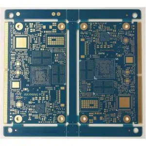
Raw Material: Fr4
Layer: 4 Layer PCB
Copper Thickness: 3oz
Surface Process: ENIG
Solder Mask: White Color
SilkScreen: Black
PCB Thickness: 1.0mm
Single size: 85.0 x 90.0 mm
Estimate PCB Manufacturing Cost, Pls send PCB File and Bom List to Sales@raypcb.com with Requirement.
4 Layer Fr4 3oz 1.0mm ENIG PCB: A Comprehensive Guide
In the world of electronic manufacturing, printed circuit boards (PCBs) are the unsung heroes that form the backbone of countless devices. Among the various types of PCBs available, the 4 Layer Fr4 3oz 1.0mm ENIG PCB stands out as a versatile and robust option. This article delves into the specifics of this PCB type, exploring its composition, advantages, applications, and manufacturing process.
Understanding the Specifications
Breaking Down the Terminology
Let’s begin by dissecting the name of this PCB to understand its key features:
- 4 Layer: This refers to the number of conductive copper layers in the PCB.
- Fr4: The base material used for the PCB substrate.
- 3oz: The thickness of the copper layers.
- 1.0mm: The overall thickness of the PCB.
- ENIG: The surface finish applied to the PCB (Electroless Nickel Immersion Gold).
The Fr4 Substrate
Fr4 (Flame Retardant 4) is a composite material consisting of woven fiberglass cloth with an epoxy resin binder. It’s widely used in PCB manufacturing due to its excellent electrical insulation properties, mechanical strength, and resistance to moisture absorption.
Copper Weight and Thickness
The “3oz” specification refers to the weight of copper per square foot on each layer. This translates to a copper thickness of approximately 105 microns (µm) per layer. The following table provides a comparison of common copper weights used in PCB manufacturing:
| Copper Weight | Thickness (µm) | Typical Applications |
|---|---|---|
| 1/2 oz | 17.5 | Low-power electronics |
| 1 oz | 35 | General-purpose PCBs |
| 2 oz | 70 | Power supplies, LED lighting |
| 3 oz | 105 | High-current applications |
| 4 oz | 140 | Extreme high-power designs |
ENIG Surface Finish
ENIG (Electroless Nickel Immersion Gold) is a popular surface finish for PCBs. It involves depositing a thin layer of nickel, followed by a thin layer of gold. This finish offers several advantages:
- Excellent surface planarity
- Good solderability
- Long shelf life
- Suitable for wire bonding
Advantages of 4 Layer Fr4 3oz 1.0mm ENIG PCBs
Enhanced Signal Integrity
The 4-layer structure allows for better signal isolation and reduced electromagnetic interference (EMI). This is particularly beneficial for high-speed digital circuits and sensitive analog designs.
Improved Power Distribution
With dedicated power and ground planes, 4-layer PCBs offer superior power distribution compared to 2-layer designs. This results in reduced noise and improved overall performance.
Higher Current Carrying Capacity
The 3oz copper thickness provides excellent current-carrying capacity, making these PCBs suitable for high-power applications.
Thermal Management
Thicker copper layers contribute to better heat dissipation, which is crucial for maintaining the reliability and longevity of electronic components.
Versatility
The combination of 4 layers, Fr4 substrate, and ENIG finish makes these PCBs suitable for a wide range of applications, from consumer electronics to industrial equipment.
Manufacturing Process
The production of 4 Layer Fr4 3oz 1.0mm ENIG PCBs involves several intricate steps:
- Material Preparation: Fr4 sheets are cut to size and cleaned.
- Inner Layer Processing:
- Copper foil is laminated to the Fr4 core.
- The circuit pattern is printed on the copper using photoresist.
- Etching removes unwanted copper, leaving the desired circuit pattern.
- Layer Alignment: The inner layers are stacked with prepreg (pre-impregnated epoxy resin) sheets between them.
- Lamination: The stack is subjected to heat and pressure to fuse the layers together.
- Drilling: Holes are drilled for vias and component mounting.
- Plating: The board is electroplated to create conductive walls in the drilled holes.
- Outer Layer Processing: Similar to inner layer processing, but for the outer layers.
- Solder Mask Application: A protective layer is applied to prevent solder bridges.
- Surface Finish: The ENIG process is applied:
- Electroless nickel plating
- Immersion gold plating
- Final Inspection and Testing: The PCBs undergo electrical testing and visual inspection.
Applications
4 Layer Fr4 3oz 1.0mm ENIG PCBs find use in various industries and applications, including:
- Power supplies and converters
- Industrial control systems
- Automotive electronics
- High-performance computing
- Telecommunications equipment
- Medical devices
- Aerospace and defense systems
Design Considerations
When designing with these PCBs, engineers should consider:
- Proper layer stackup for optimal signal integrity
- Adequate copper pour for power distribution and heat dissipation
- Impedance control for high-speed signals
- Proper via placement and sizing
- Compliance with manufacturing design rules
Frequently Asked Questions (FAQ)
Q1: What is the maximum current capacity of a 3oz copper trace?
A1: The current capacity depends on various factors such as trace width, ambient temperature, and acceptable temperature rise. As a general guideline, a 1mm wide trace on an outer layer can safely carry about 5-7 amperes. However, it’s crucial to perform proper thermal calculations for your specific design.
Q2: How does the ENIG finish affect solderability?
A2: ENIG provides excellent solderability due to the gold layer, which prevents oxidation of the underlying nickel. It maintains its solderability for an extended period, typically 12 months or more when stored properly.
Q3: Can I use lead-free solder with these PCBs?
A3: Yes, 4 Layer Fr4 3oz 1.0mm ENIG PCBs are fully compatible with lead-free soldering processes. The ENIG finish is particularly well-suited for lead-free solders, which typically require higher reflow temperatures.
Q4: How does the 1.0mm thickness affect the PCB’s flexibility?
A4: At 1.0mm thickness, these PCBs are relatively rigid and not intended for flexible applications. If flexibility is required, thinner substrates (e.g., 0.4mm or 0.6mm) would be more appropriate.
Q5: What is the typical impedance range achievable with these PCBs?
A5: The achievable impedance range depends on the specific layer stackup and trace geometry. Generally, impedances between 50Ω and 100Ω are readily achievable. For precise impedance control, it’s best to work closely with your PCB manufacturer during the design phase.
Conclusion
4 Layer Fr4 3oz 1.0mm ENIG PCBs offer a robust and versatile solution for a wide range of electronic applications. Their combination of thick copper layers, multi-layer design, and high-quality surface finish makes them ideal for demanding projects requiring high current capacity, excellent signal integrity, and long-term reliability. By understanding the characteristics and manufacturing process of these PCBs, engineers and designers can leverage their full potential to create cutting-edge electronic products.