Every homeowner knows that excessive humidity can be a significant issue for everything from your walls to water pipes. If you don’t have a humidity sensor in your home, you may not know how high the humidity is. As a result of a lack of action, you may end up with larger issues as time goes on. Few people also realize that maintaining optimum humidity levels indoors can impact the quality of the air you breathe.
There are several ways that excessive humidity can affect air quality indoors. So clearly understanding the role humidity plays in your home is essential. It will help you to maintain the healthiest level of indoor air possible. Most importantly, you must use a hygrometer to monitor humidity levels in your home, one that works.
Humidity and You
Your body consists of about 60% water, and for good health, your body should maintain relative humidity (RH) percentage of anywhere from 40% to 60%. Below 40% to the point where dehydration begins is an arid environment. Conditions less than 35% RH are unsuitable for outdoor activities. Above 60% RH can be dangerous, especially for infants and people with respiratory issues.
There are several positive connections as a result of the close connection between humidity levels and temperature. For example, when your air is humid, it also tends to be warm. This is because moisture evaporates at warmer temperatures. So if you have low humidity, you are losing a good bit of valuable heat energy in the form of humidity. In areas that experience lower indoor temperatures due to lower indoor humidity levels, it can lead to overheating issues for humans and animals.
What Is Humidity?
We define humidity as the ratio of water vapor in the air to the dry air surrounding it. The human body consists of about 60% water, so humidity levels are always relative to your body’s makeup. The lower your humidity levels, the more susceptible you are to dehydration.
For example, a relative humidity (RH) of 50% means the air in the room is half full of moisture. Relative humidity of 40% means the air is 40% full of moisture.
Why does it Matter?
Some common symptoms associated with high humidity include:
1. Perspiration
Excessive perspiration can lead to blisters, rashes, and fungal infections on the skin. It can increase your risk for athlete’s injuries and even cause permanent damage to your skin.
2. Mold
High humidity levels are a breeding ground for mold, leading to personal allergies and respiratory problems.
3. Moisture damage
You must maintain the humidity level in your room. So, the wooden furniture in your house will not absorb the moisture and swell, leading to cracking and decay.
4. Deformation
Forced air systems can’t handle humidity levels over 30%. So they tend to overwork themselves and wear out prematurely. This results in higher energy bills.
What are humidity sensors?
Humidity sensors, also known as hygrometers, are easy to install, accurate, and inexpensive. When installed correctly and maintained, they can be responsible for decreasing your energy bills. They also improve your home’s indoor air quality. Suppose the sensor is anything less than accurate. In that case, it can lead to serious problems in your home, so you must use a quality model from a reputable company with good customer service.
In many cases, you might find a home temperature and humidity sensor in your home’s HVAC system. So, it is therefore built directly into your thermostat. If you decide to go this route, it may be challenging to determine the humidity level at a specific part of your home. So consider that as well when shopping for a device.
Most home heat and humidity sensors include advanced features such as:
1. Wireless monitoring – You can position it anywhere in your house and monitor it from any computer that has an Internet connection.
2. Remote setting for home comfort – You can use the device to set the ideal humidity level in your home and adjust it as needed.
How Do You Set It Up?
The setup process for a humidity sensor is pretty straightforward, but you want to be sure that you go over all of the instructions before you begin. You can find most manuals online, or you can call your manufacturer’s customer support line if you have an issue. In general, here is what goes into setting up a humidity sensor:
1. Find a location
Most devices will include a recommended location, but that’s fine if you want to move it. You need to make sure the sensor is about 4 feet off of the ground and away from any large metal items such as metal pipes or cabinets.
2. Test it
Put batteries in your sensor to test that it works properly. Ideally, you should see a reading between 40% and 60% relative humidity.
3. Connect it to your HVAC system
If you have a humidistat, make sure that you hook the sensor’s wire into the same control box connected to your humidistat.
4. Calibrate it
Most sensors will have a built-in calibration function that you should perform near the end of installing them. But if you don’t, you may need to take your sensor back for a checkup.
5. Place it in the right spot
Make sure you place it in a spot to expose it to the correct amount of air and temperature. But far enough away from any heating or cooling vents won’t get disturbance by unwanted air movement.
6. Monitor it
After setting up the calibration function, you should never need to do anything else to your sensor. Still, you should continue to monitor its readings at least once every month during the heating and cooling seasons.
How do humidity sensors work?
There are two basic hygrometers for indoor use: electronic and mechanical. Mechanical versions are usually more accurate and durable. But electronic models have improved so much in recent years that many homeowners prefer them for their ease of use. Manufacturers market many of these products as “smart” home products. They can adjust their configurations based on your particular needs. So, it’s essential to understand the entire process before buying.
An electronic hygrometer is a virtual device. It will provide you with a relative humidity reading based on the amount of moisture in the air. Since moisture level sensors are fairly accurate and simple to use, they make fantastic additions to your home or office. When it comes to relative humidity, a modern model will work with a relatively simple process: you’ll push a button. It will tell you the current humidity in your home.
The type of sensor you choose depends on what you want to measure. Still, if you’re looking for one that tells you the relative humidity level, most electronic models will show this information.
Why Would You Use a Humidity Sensor?
There are several reasons why you would want to monitor the humidity level in your home, and they include:
1. Keep your air conditioning bill under control
If you have a relative humidity sensor installed, you may find that your heating and cooling system works less frequently when your home is humid. This is because the moisture level in the air isn’t so high that it needs removing.
2. Reduce mold
If you have a problem with mold in your home, it’s important to maintain humidity levels below the 80% range. Some models can help you maintain this by adjusting your home’s temperature, but there are other options as well. A more advanced model will have a built-in humidistat and automatically regulate the temperature based on your humidity level.
3. Save money on your water bill
Suppose you have a humidity sensor installed in your HVAC system. In that case, it may be able to save you money on water, especially if your home is not as humid as the manufacturer recommended setting.
4. Choose the right air filter
Some air filters can reduce certain types of mold and mildew, and others can remove allergens from the air. If you have a moisture sensor installed, you can choose the right filters for your needs.
5. Examine the airflow
You might be able to tell if there are air leaks in your HVAC system by placing a humidity sensor in various spots around your house.
6. Decide on heating and cooling options
If you have a humidity sensor, you’ll be able to make decisions about heating and cooling that consider your home’s relative humidity.
7. Health reasons
If you have acidic air or dry air symptoms, a humidity sensor can help you detect this issue and correct it before it affects your health.
8. Improve your home’s quality of life
You might enjoy a more comfortable environment if you use a humidity sensor in your HVAC system.
9. Avoid potential problems
Low relative humidity levels can lead to mold and mildew growth. It can cause significant problems for the structure of your home.
Factors to consider when choosing the type of humidity sensor
Here is a thing to consider to help you make an informed decision before choosing one for your home. Considerations include:
1. Sensor Design
Most humidity sensors will have a simple design and will look similar to a thermometer with a long shaft and a small circular display on top. However, you should make sure that the sensor you choose will fit in your HVAC system correctly before you buy it.
2. Location
Many humidity sensors work perfectly with HVAC systems. But others we will use for spot-checking relative humidity levels in specific rooms or areas.
3. Materials
We can make sensors from various materials, including metal (like steel) or plastic.
4. Size
You may want to place your sensor in a specific part of your HVAC system. So you should make sure that you can find one that’s the right size.
5. Durability
If you want a sensor that will be useful for several years, it’s essential to choose durable and well-made.
6. Uses
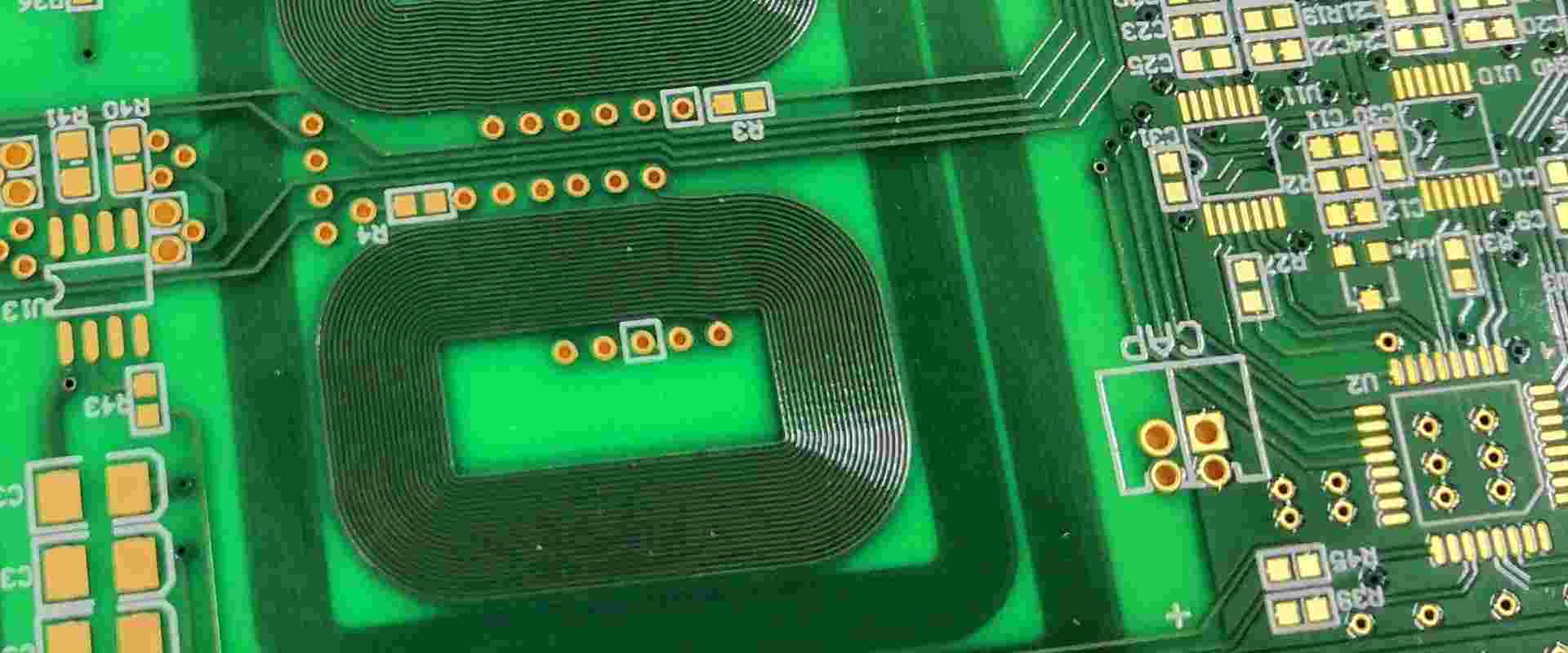
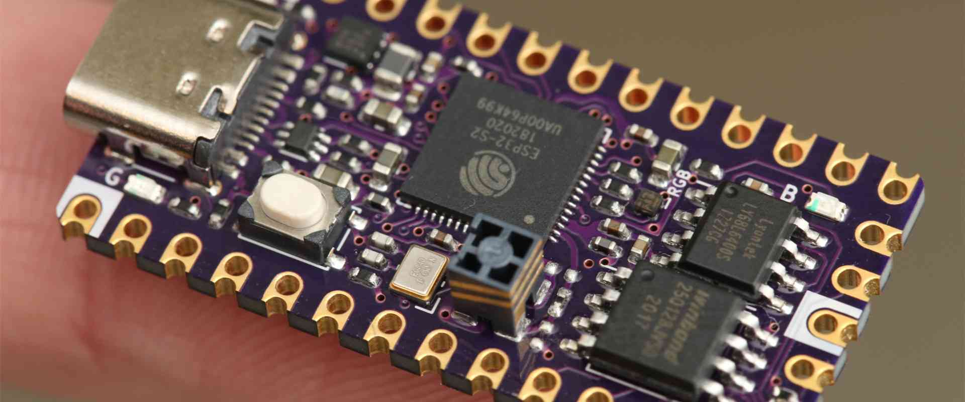
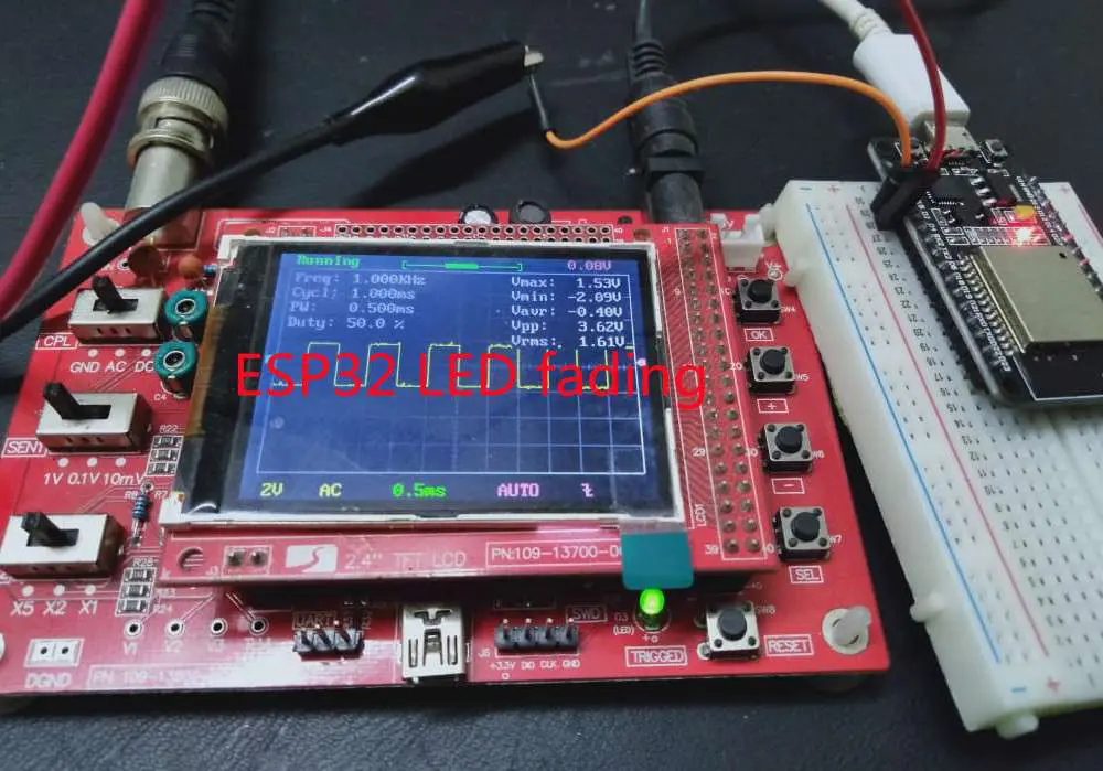
If you have a humidifier, dehumidifier, or air purifier installed in your home, you’ll need to buy humidity sensors arduino that work with these products.
7. Programmable
Many humidity sensors today are digital. You can program them to tell you the relative humidity of your home or office based on the time of day or the prevailing weather conditions.
8. Additional features
Some humidity sensors offer additional features, such as alarms that go off if the moisture level in your air reaches a certain point.
9. Price
If you’re trying to save money by installing an inexpensive sensor in your HVAC system, you might get frustrated when it fails after a few months of use.
10. Warranty
The right manufacturer will offer a warranty that protects you against problems with your sensor. So make sure that you cover these details before making your final choice.
Types of humidity sensors
Since humidity is a factor in so many indoor environments, several different sensors are available.
1. Whole-Home Humidity System
Whole-home humidity systems will provide accurate readings for the air in your home. You can use it to save money and improve your overall quality of life. They come with numerous individual humidity sensors positioned tactically through the house. They work best with the HVAC system. These sensors can monitor more areas than just your home, so you can use them in other rooms if you need to do spot-checking.
The distinctive sensors connect or link via Bluetooth, Wi-Fi, or radiofrequency to a base station unit. You can find it near your HVAC system. The base station uses cellular technology to pass the information from the individual sensors to a smartphone. It can also pass it to other devices so that you can remotely monitor the humidity levels in your home. Some whole-home systems will adjust various aspects of your HVAC system based on the moisture level reported by the sensors.
2. Point Source Humidity Sensor
A point source humidity sensor is suitable for spot-checking rather than to install in your HVAC system. We usually house these sensors in a durable case resistant to the elements. You can place them throughout your home or office to get an accurate picture of relative humidity levels. A digital point source humidity sensor will usually have a display. It can show you the current reading for relative humidity and the temperature inside your air space.
Here, a relative humidity sensor can help measure whether your HVAC system is working properly. It can also help you decide whether you need to use a humidifier or dehumidifier. Many point source sensors are suitable for outdoor use. So, they are helpful in places where humidity can affect your home’s exterior quality of life. Some point source humidity sensors will include an alarm that will tell you if moisture levels get too high. It can help extend the life of your HVAC system.
3. Smart Home Humidity Sensor System
A smart home humidity sensor system is suitable for use in the comfort of your own home. This can include sensors that are part of a whole-home system. But you can also purchase stand-alone units that will be helpful precisely to monitor the humidity inside your house. Smart home humidity sensors connect to a central gateway. Each piece of equipment can communicate with the others by Wi-Fi or Bluetooth.
This allows you to monitor your air quality from any location that you have internet access. These systems will also record logs of the air quality in your home and display them on a website wherever you have an internet connection. A smart home humidity sensor system can help you effectively use a humidifier or dehumidifier. It will also allow you to control your home’s temperature and make it easy for you to find out when the relative humidity in any given room gets too high.
4. Capacitive humidity sensors
These temperature and humidity sensors are suitable for working in a stand-alone humidity sensor that won’t work. For example, they may be helpful if you want to use your sensor in an office or other environment where there isn’t a lot of space. These sensors will usually include a display. It will connect to the outside of your HVAC system with the help of a standard wire or adhesive pad that allows it to adhere directly to your outdoor unit. It uses a capacitor consisting of two electrode layers to measure the amount of moisture in the air. We can then use the readings from these sensors to determine whether the HVAC system has water damage. You can also use them to determine whether your HVAC system is working.
5. Resistive humidity sensors
We also refer to it as a hygristor or an electrical conductivity sensor. A resistive humidity sensor is suitable for use in very high moisture environments. It includes plants and aquariums. They consist of a conductive material similar to a resistor on top of a non-conductive sensing substrate, such as plastic or paper. This is the resistance of the material changes when we introduce moisture into it. This change causes a change in electrical current, which we can measure. Resistive humidity sensors can determine the relative humidity where there is moisture. They include normal and very high moisture environments.
6. Thermal conductivity humidity sensors
Thermal conductivity sensors, also known as thermal capacitance, are helpful in high-temperature environments. They use the thermal conductivity of materials to detect changes in humidity. We construct the sensor from a capacitor and a heating element. The sensor’s output will also change as the air temperature and relative humidity change. The thermal conductivity sensor uses two thermocouple junctions. One thermocouple junction can help sense temperature. That is the other for humidity measurement.
What Can Humidity Sensors Control?
Humidity sensors control many functions inside your home, including temperature and relative humidity.
Thermostats
Thermostats can regulate the temperature inside your home or office and be convenient if you want to control specific rooms or areas. You do not have to adjust each room’s thermostat individually. Instead, you can use a central station that will regulate temperatures throughout your entire building. It is usually possible to program these thermostats to turn on and off automatically, based on any detected conditions.
We can use humidity sensors similarly by opening and closing water valves in the air ducts of your HVAC system. We will connect these valves to the thermostats used throughout your building. Many homeowners find this type of approach to controlling temperature more convenient. It can be inconvenient if several rooms share a single thermostat.
Thermostats are more common in commercial buildings than in residential properties. But they can also be helpful for homeowners who live in older homes with stubborn heating and cooling systems.
Temperature Sensors
Temperature sensors are another option that you can use to control the temperature inside your home or office. We can use these sensors in conjunction with a thermostat or a humidistat. You will have a complete picture of the temperature inside your space no matter where you install them.
In addition to controlling your HVAC system, temperature sensors can help alert you if the temperature in a room gets too hot or too cold.
What Are The Limitations of Temperature & Humidity Sensors?
Because these sensors are so close to the temperature and moisture in your home, they have their limitations.
1. Moisture is Not A Pure Measurement
The moisture you feel in your home is a combination of temperature and relative humidity. When you measure moisture, you measure the temperature and relative humidity levels simultaneously. This is because they are so closely linked.
2. Temperature Sensors Can Be Unreliable
We can build temperature sensors and thermometers in a variety of different ways. This is one reason why some sensors can give inaccurate readings. When you take moisture readings, it is essential to make sure that you have accurate temperature readings.
3. Humidity Sensors Are Not Always Accurate
Just because you have a humidity sensor in your home does not mean that your home is very humid in the middle of the day. This type of humidity sensor only tells you whether the relative humidity is too high or too low. It can be challenging to determine what level is from only reading one number from the sensor.
Conclusion
Temperature and humidity sensors can be helpful tools in your home or office. But they can only provide you with a partial picture of the climate inside your building. Contact RayMing PCB and Assembly to learn more about how to use these sensors. You will also learn what precautions you need to take to get the most accurate readings from them. If you want to install humidity sensors in your home or office, choosing a sensor that can give you the most accurate results is essential.