How to Find Total Number of SMD Pads in Design

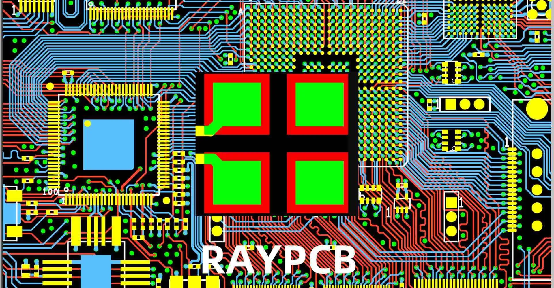
Accurately counting the total number of Surface Mount Device (SMD) pads in a PCB design is crucial for manufacturing planning, cost estimation, and quality control. This comprehensive guide explores various methods, tools, and best practices for determining the exact number of SMD pads in your design.

YouTube video

Understanding SMD Pad Types

Common SMD Pad Categories

Pad TypeDescriptionCommon Usage
RectangularBasic rectangular shapeGeneral components
RoundCircular shapePin 1 indicators, vias
CustomSpecial shapesRF, thermal applications
OblongElongated padsMechanical stability
ThermalWith thermal reliefPower components

Standard Package Footprints

Package TypeNumber of PadsCommon Applications
SOT-233-6Small transistors
SOIC-88ICs, op-amps
QFP32-256Microcontrollers
BGA4-1000+Complex processors
0402/0603/08052Passive components

Manual Counting Methods

Component-Based Counting

Process Steps

  1. Create component categories
  2. Count components per category
  3. Multiply by pad count
  4. Sum all categories

Component Grouping Example

Component TypePad CountQuantity
0402 Resistors2100
SOIC-8810
QFP-44442
LEDs220

Layer-Based Counting

Layer Analysis Process

LayerWhat to CountConsiderations
Top LayerAll SMD padsExclude through-holes
Bottom LayerAll SMD padsExclude through-holes
Inner LayersN/ASMD pads only on outer layers

Automated Counting Methods

CAD Software Tools

Common Software Features

FeatureDescriptionAccuracy
Pad CounterDirect pad countingVery High
BOM AnalysisComponent-based countingHigh
Layer StatisticsLayer-based countingHigh
Design RulesPad verificationMedium

Software-Specific Methods

SoftwareTool LocationFeatures
AltiumReports โ†’ Board StatisticsComplete pad analysis
KiCadPCB Editor โ†’ StatisticsBasic pad counting
EagleULP ScriptsCustomizable counting
OrCADReports โ†’ StatisticsDetailed analysis

Verification Methods

Cross-Checking Techniques

MethodReliabilityTime Required
Visual InspectionMediumHigh
BOM VerificationHighMedium
Layer ComparisonHighLow
Script ValidationVery HighLow

Common Error Sources

Error TypeCausePrevention
Missing PadsHidden layersLayer visibility check
Double CountingOverlapping componentsComponent placement check
Wrong ClassificationIncorrect pad typesDesign rule check
Script ErrorsSoftware bugsMultiple verification methods

Documentation and Reporting

Report Components

Essential Information

Information TypePurposeFormat
Total Pad CountManufacturing planningNumeric
Pad DistributionLayer balancePercentage
Component SummaryBOM verificationTable
Special Pad TypesProcess planningList

Report Format Example

CategoryTop LayerBottom Layer
SMD Pads450320
Thermal Pads128
Custom Pads42
Total466330

Manufacturing Considerations

Pad Count Impact

Process Planning

AspectImpactConsideration
Stencil DesignDirectAperture count
Assembly TimeDirectPick-and-place programming
Inspection PointsDirectAOI programming
Defect RateIndirectQuality control planning

Cost Implications

FactorRelationshipCost Impact
Stencil CostLinearMedium
Assembly TimeLinearHigh
Testing TimeLinearMedium
Rework RiskExponentialHigh

Quality Control

Inspection Methods

MethodCoverageTime Required
Visual100%High
AOI100%Low
X-RaySelectiveMedium
Flying Probe100%High

Defect Analysis

Defect TypeRelated to Pad CountPrevention Method
Solder BridgesYesProper spacing
Missing SolderYesStencil design
MisalignmentYesFiducial placement
Component DamageNoProper handling

Frequently Asked Questions

Q1: Why is accurate pad counting important?

A: Accurate pad counting is crucial for:

  • Manufacturing cost estimation
  • Assembly time planning
  • Quality control processes
  • Material requirements calculation
  • Testing procedure development Inaccurate counts can lead to production delays and cost overruns.

Q2: What’s the most reliable method for counting SMD pads?

A: The most reliable method is a combination of:

  • Automated CAD software counting
  • BOM-based verification
  • Cross-checking between different methods
  • Manual verification of special cases This multi-layered approach helps ensure accuracy.

Q3: How do I handle special pad types in the count?

A: Special pad types should be:

  • Clearly identified in the design
  • Counted separately from standard pads
  • Documented in the BOM
  • Verified with manufacturing team
  • Included in final count with appropriate notes Special attention to thermal pads and custom shapes is essential.

Q4: What are common sources of pad counting errors?

A: Common errors include:

  • Overlooking components on bottom layer
  • Double-counting dual-side components
  • Missing thermal or special pads
  • Incorrect component footprint definitions
  • Software calculation errors Regular verification and cross-checking helps prevent these errors.

Q5: How can I optimize my design for pad count verification?

A: Optimization strategies include:

  • Using consistent component libraries
  • Maintaining organized layer structure
  • Implementing clear naming conventions
  • Regular design rule checks
  • Documenting special cases Good organization from the start makes verification easier.

Conclusion

Finding the total number of SMD pads in a PCB design requires a systematic approach combining automated tools, manual verification, and proper documentation. Success depends on understanding different pad types, using appropriate counting methods, and implementing proper verification procedures. By following the guidelines in this document and maintaining good documentation practices, you can ensure accurate pad counts for your PCB designs.

How to DIY A Raspberry Pi Expansion Board

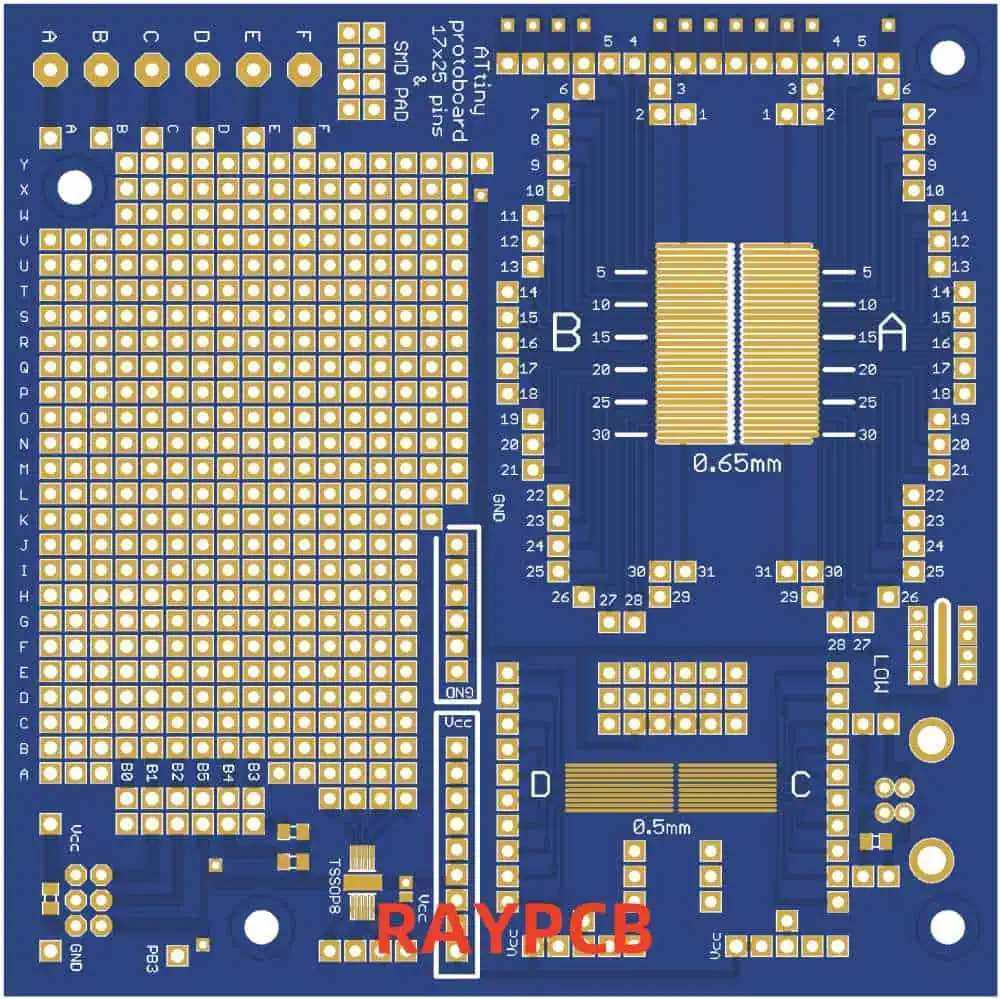
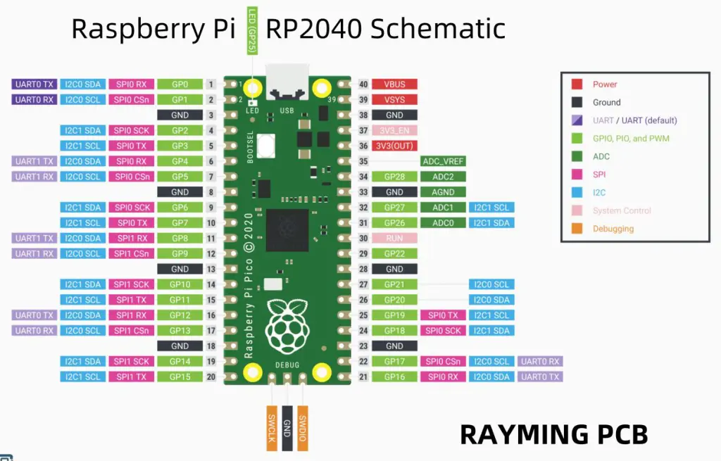
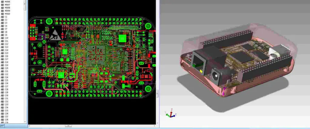
Creating a custom expansion board (HAT – Hardware Attached on Top) for your Raspberry Pi allows you to extend its capabilities and create specialized solutions for your projects. This comprehensive guide will walk you through the process of designing and building your own Raspberry Pi expansion board, from initial planning to final testing.

YouTube video

Understanding Raspberry Pi Hardware

GPIO Pin Layout

Pin Configuration Table

Pin TypeNumber AvailableCommon Uses
Power (3.3V)2 pinsLow-power peripherals
Power (5V)2 pinsHigher power devices
Ground8 pinsCircuit completion
GPIO26 pinsDigital I/O, Special functions
I2C2 pinsSerial communication
SPI5 pinsHigh-speed serial interface
UART2 pinsSerial communication

Special Function Pins

Pin FunctionGPIO NumbersNotes
I2C SDAGPIO 2Primary I2C data line
I2C SCLGPIO 3Primary I2C clock line
SPI MOSIGPIO 10SPI data out
SPI MISOGPIO 9SPI data in
SPI SCLKGPIO 11SPI clock
UART TXGPIO 14Serial transmit
UART RXGPIO 15Serial receive

Planning Your Expansion Board

Requirements Analysis

  1. Functional Requirements
    • Purpose of the board
    • Required interfaces
    • Power requirements
    • Size constraints
  2. Technical Specifications
    • Voltage levels
    • Current requirements
    • Communication protocols
    • Component selection

Design Considerations Matrix

AspectConsiderationsImpact
Power SupplyVoltage regulation, current capacityBoard reliability
Form FactorHAT specifications, mounting holesPhysical compatibility
InterfaceGPIO usage, protocolsFunctionality
ComponentsAvailability, costProduction feasibility
AssemblyThrough-hole vs SMDManufacturing process

Circuit Design

Essential Components

Power Management

ComponentPurposeSpecifications
Voltage RegulatorPower stability5V to 3.3V conversion
Protection DiodesReverse voltage protectionSchottky type
Bypass CapacitorsNoise reduction0.1ยตF and 10ยตF
FuseOvercurrent protectionPTC or regular

ID EEPROM

The HAT specification requires an ID EEPROM that contains board information:

InformationDescriptionRequired
Vendor InfoManufacturer detailsYes
Product UUIDUnique identifierYes
GPIO MapPin usage definitionYes
Device TreeHardware descriptionOptional

Level Shifting

Voltage LevelDirectionCircuit Type
5V to 3.3VInputVoltage divider
3.3V to 5VOutputMOSFET shifter
MixedBidirectionalIC-based shifter

PCB Design

Layout Guidelines

Component Placement

Component TypePlacement PriorityConsiderations
ConnectorsHighEdge accessibility
Power ComponentsHighHeat dissipation
Sensitive CircuitsHighNoise isolation
Support ComponentsMediumSpace optimization

Layer Stack-up

LayerPurposeRequirements
TopComponents, SignalsMain routing
GroundGround planeSolid pour
PowerPower distributionSplit planes
BottomComponents, SignalsAdditional routing

Critical Dimensions

DimensionSpecificationTolerance
Board Size65mm x 56mmยฑ0.1mm
Mounting Holes3.5mm diameterยฑ0.1mm
Edge Clearance3mm minimumยฑ0.5mm
Stack Height2.5mm maximumยฑ0.2mm

Component Selection

Common Components List

Component TypeRecommended ValuesPackage
ResistorsE24 series0805/THT
Capacitors0.1ยตF, 10ยตF0805/THT
LEDs3.3V compatible0805/THT
Connectors2.54mm pitchThrough-hole
EEPROMCAT24C32SOIC-8

Interface Components

InterfaceComponent ExampleFeatures
I2CPCA9615Level shifting, buffering
SPI74LVC125Level translation
UARTMAX3232RS232 conversion
GPIO74LVC245Buffering, protection

Assembly Process

Tools Required

ToolPurposeEstimated Cost
Soldering IronComponent assembly$30-100
MultimeterTesting$20-50
TweezersComponent handling$5-15
MagnifierInspection$10-30
Solder WickRework$5-10

Assembly Steps Checklist

  1. Preparation
    • Component organization
    • Tool setup
    • Board cleaning
  2. Assembly Sequence
    • Low-profile components first
    • Temperature-sensitive components
    • Mechanical components last

Testing and Verification

Test Procedures

Test TypeMethodEquipment Needed
ContinuityPoint-to-point testingMultimeter
Power SupplyVoltage measurementsPower supply, Multimeter
GPIO FunctionSignal testingLogic analyzer
InterfaceProtocol verificationOscilloscope

Common Issues

ProblemPossible CauseSolution
No PowerBad connectionsCheck soldering
GPIO FailureWrong voltage levelsVerify level shifting
EEPROM IssuesI2C address conflictCheck address setting
NoisePoor groundingImprove ground plane

Frequently Asked Questions

Q1: What are the minimum requirements for a Raspberry Pi HAT?

A: The minimum requirements include:

  • 40-pin GPIO header
  • Mounting holes in the correct position
  • ID EEPROM with vendor and product information
  • Proper prototype board dimensions (65mm x 56mm)
  • 3.3V compatible GPIO connections Consider these as the baseline and add features as needed for your specific application.

Q2: How do I protect my expansion board and the Raspberry Pi?

A: Implement these protection measures:

  • Use voltage level shifters where needed
  • Include reverse polarity protection
  • Add current limiting resistors
  • Implement proper bypassing
  • Use ESD protection on exposed pins
  • Include a fuse or current limiter Regular testing during development helps ensure protection is adequate.

Q3: What tools and skills are needed for DIY expansion board creation?

A: Essential tools and skills include:

  • PCB design software knowledge
  • Basic electronics understanding
  • Soldering equipment and skills
  • Testing equipment (multimeter minimum)
  • Understanding of Raspberry Pi GPIO Start with simple designs and gradually increase complexity as skills improve.

Q4: How can I ensure my expansion board is reliable?

A: Follow these guidelines:

  • Use quality components
  • Implement proper power management
  • Include protection circuits
  • Follow PCB design best practices
  • Test thoroughly before deployment
  • Document all design decisions Regular review and testing throughout the development process is crucial.

Q5: What are common mistakes to avoid when designing a HAT?

A: Common pitfalls include:

  • Incorrect voltage levels
  • Poor power supply design
  • Insufficient protection circuits
  • Wrong EEPROM configuration
  • Mechanical interference
  • Poor documentation Always prototype and test thoroughly before finalizing the design.

Conclusion

Creating a DIY Raspberry Pi expansion board requires careful planning, attention to detail, and a systematic approach to design and implementation. Success depends on following HAT specifications, proper component selection, careful PCB layout, and thorough testing. By following the guidelines in this document and maintaining good documentation practices, you can create reliable and functional expansion boards that enhance your Raspberry Pi projects.

How to Create a Microcontroller Circuit Board

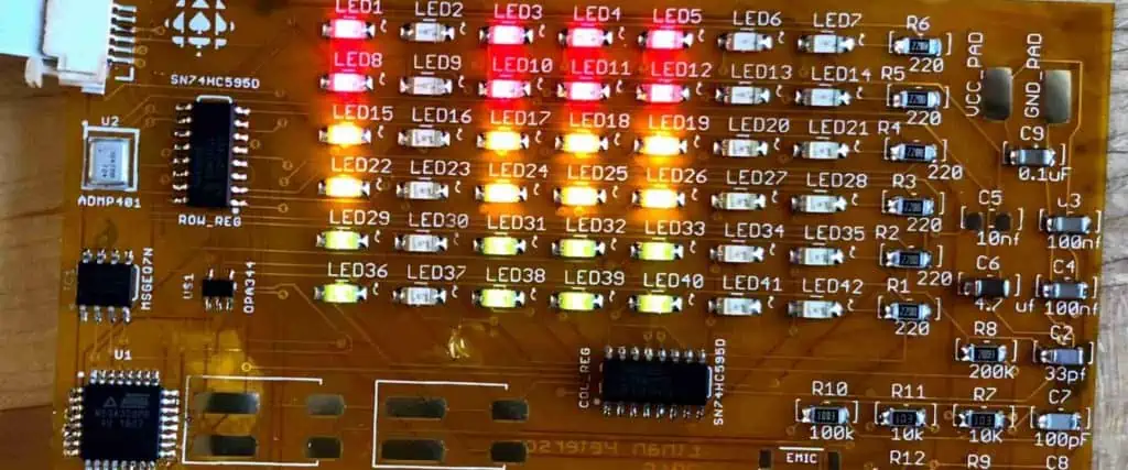
Creating a microcontroller circuit board is a complex but rewarding process that combines hardware design, programming, and electronic engineering principles. This comprehensive guide will walk you through the essential steps, considerations, and best practices for designing and implementing a successful microcontroller-based circuit board.

YouTube video

Planning and Requirements

Project Specifications

Before beginning the design process, establish clear project requirements including:

  1. Performance requirements
  2. Size constraints
  3. Power requirements
  4. Environmental conditions
  5. Cost limitations

Microcontroller Selection

Selection Criteria Matrix

rix
FeatureImportanceConsiderations
Processing SpeedHighApplication demands, real-time requirements
Memory (Flash/RAM)HighProgram size, data storage needs
I/O PinsCriticalNumber of peripherals, expansion needs
Power ConsumptionMediumBattery life, heat dissipation
CostMediumBudget constraints, production volume
Package TypeMediumBoard space, assembly method

Common Microcontroller Families

FamilyManufacturerArchitectureTypical Applications
ATmegaMicrochip8-bit AVRGeneral purpose, hobby projects
STM32ST32-bit ARMIndustrial, complex applications
PICMicrochip8/16/32-bitIndustrial control, automotive
ESP32Espressif32-bitIoT, wireless applications

Circuit Design

Essential Components

Power Supply Section

  1. Voltage Regulators
    • Linear regulators
    • Switching regulators
    • Low-dropout (LDO) regulators
  2. Protection Circuits
    • Reverse polarity protection
    • Overcurrent protection
    • ESD protection

Power Supply Selection Guide

TypeEfficiencyHeat OutputCostComplexity
LinearLowHighLowSimple
SwitchingHighLowMediumComplex
LDOMediumMediumLowSimple

Critical Circuits

Reset Circuit

  • Power-on reset
  • Manual reset button
  • Supervisory IC

Crystal Oscillator

Peripheral Interfaces

InterfaceSpeedPins RequiredCommon Uses
UARTLow-Medium2-4Debug, communication
SPIHigh4Sensors, displays
I2CMedium2Multiple device control
ADCVaries1 per channelAnalog sensing

PCB Design

Layout Considerations

Component Placement

Component TypePlacement PriorityConsiderations
CrystalHighestClose to MCU, minimal traces
Bypass CapsHighClose to power pins
Power SupplyHighThermal management
ConnectorsMediumEdge placement, accessibility

Layer Stack-up

Typical 4-Layer Stack-up

LayerPurposeConsiderations
TopComponents, SignalsComponent density
Inner 1GroundContinuous plane
Inner 2PowerSplit planes as needed
BottomComponents, SignalsAdditional routing

Design Rules

Trace Width Guidelines

Current (A)Minimum Width (mil)Temperature Rise (ยฐC)
0.51010
12015
23020
35025

Programming and Debug

Programming Interfaces

Common Programming Methods

MethodProsConsUsage
JTAGFull debug capabilityMore pinsDevelopment
SWDReduced pin countLimited to ARMDevelopment
ISPSimpleLimited debugProduction
BootloaderNo external programmerTakes flash spaceField updates

Debug Features

  1. Hardware Debug
    • Breakpoints
    • Single-stepping
    • Register inspection
    • Memory viewing
  2. Software Debug
    • Serial printf debugging
    • LED status indicators
    • Debug pins

Testing and Verification

Test Procedures

Functional Testing Matrix

Test TypeDescriptionEquipment Needed
Power TestVoltage levels, current drawMultimeter, power supply
Signal TestDigital/analog signalsOscilloscope
Interface TestCommunication protocolsLogic analyzer
Stress TestTemperature, load testingEnvironmental chamber

Common Issues and Solutions

IssuePossible CauseSolution
No PowerWrong voltage, reversed polarityCheck power connections
No ProgrammingWrong connections, fusesVerify programmer setup
Unstable OperationPoor bypass caps, noiseImprove decoupling
Communication FailsWrong voltage levels, timingCheck protocol settings

Production Considerations

BOM Management

Component Selection Criteria

CriteriaImportanceImpact
AvailabilityHighProduction delays
CostHighProduct pricing
QualityHighReliability
Lead TimeMediumInventory management

Assembly Options

MethodAdvantagesDisadvantagesVolume Range
Hand AssemblyLow startup costLabor intensive1-100
Pick and PlaceFast, consistentHigh setup cost100+
MixedFlexibleComplex management50-500

Documentation

Required Documents

  1. Design Files
    • Schematics
    • PCB layouts
    • BOM
    • Assembly drawings
  2. Technical Documentation
    • Specifications
    • Test procedures
    • Programming guides
    • Debug procedures

Frequently Asked Questions

Q1: What are the most important factors to consider when selecting a microcontroller?

A: The key factors are:

  • Processing power requirements
  • Memory needs (both Flash and RAM)
  • Number and type of peripherals needed
  • Power consumption requirements
  • Development tool availability and cost
  • Unit cost at expected production volumes Always consider future expansion needs when making the selection.

Q2: How do I determine the right power supply configuration for my board?

A: Consider these factors:

  • Input voltage range requirements
  • Current requirements for all components
  • Efficiency requirements
  • Heat dissipation constraints
  • Noise sensitivity of circuits Choose between linear, switching, or LDO regulators based on these requirements.

Q3: What are the essential design considerations for reliable operation?

A: Key considerations include:

  • Proper bypass capacitor placement
  • Clean power supply design
  • Ground plane integrity
  • EMI/EMC considerations
  • Thermal management
  • Protection circuits Regular design reviews and testing help ensure reliability.

Q4: How can I make my board easier to manufacture?

A: Implement these practices:

  • Use standard component sizes
  • Maintain adequate spacing
  • Include fiducials for automated assembly
  • Use standard PCB thickness and copper weights
  • Include test points
  • Design for panel assembly
  • Consider pick-and-place machine requirements

Q5: What are common debugging approaches for microcontroller boards?

A: Common debugging methods include:

  • Using hardware debuggers (JTAG/SWD)
  • Including LED indicators
  • Adding test points
  • Implementing debug UART
  • Using logic analyzers
  • Including current measurement points Choose methods appropriate for your development needs and production testing requirements.

Conclusion

Creating a microcontroller circuit board requires careful planning, attention to detail, and consideration of multiple factors throughout the design process. Success depends on making appropriate choices in microcontroller selection, circuit design, PCB layout, and testing procedures. By following the guidelines outlined in this document and maintaining good documentation practices, you can create reliable and functional microcontroller-based circuit boards that meet your project requirements.

How to Clean PCBs after Surface Mount Soldering

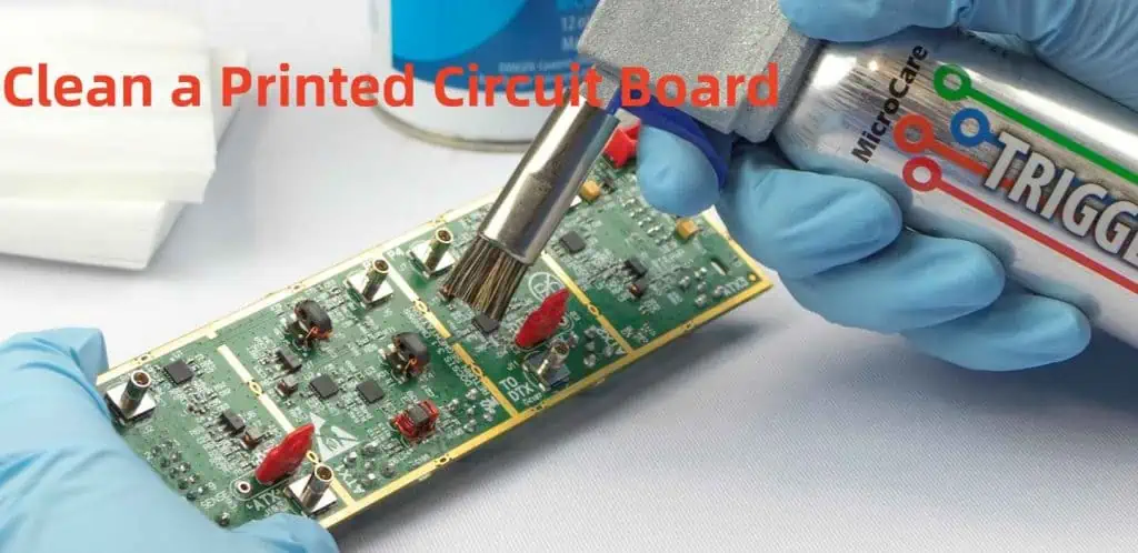
Proper cleaning of printed circuit boards (PCBs) after surface mount soldering is crucial for ensuring optimal performance, reliability, and longevity of electronic devices. This comprehensive guide covers everything from understanding the need for PCB cleaning to implementing effective cleaning protocols and maintaining quality standards.

Why Clean PCBs?

Contamination Sources

Surface mount technology (SMT) assembly processes can leave various contaminants on PCBs that may cause:

YouTube video

Common Contaminants

Contaminant TypeSourcePotential Impact
Flux ResiduesSoldering ProcessSignal interference, corrosion
Solder BallsReflow ProcessShort circuits, visual defects
FingerprintsManual HandlingComponent degradation, coating issues
Dust/DebrisEnvironmentThermal problems, electrical issues
Chemical ResiduesPrevious ProcessesLong-term reliability problems

Pre-Cleaning Assessment

PCB Cleaning
PCB Cleaning

Determining Cleaning Requirements

Before initiating the cleaning process, consider these factors:

  1. Board complexity
  2. Component sensitivity
  3. Environmental conditions
  4. End-product requirements
  5. Regulatory compliance

Cleaning Process Selection Matrix

FactorNo-Clean ProcessAqueous CleaningSolvent Cleaning
CostLowMediumHigh
Environmental ImpactLowMediumHigh
Cleaning EffectivenessLimitedHighVery High
Process ComplexitySimpleModerateComplex
Equipment RequiredMinimalModerateExtensive

Cleaning Methods and Techniques

Manual Cleaning

Manual cleaning is suitable for low-volume production or prototype boards. Key considerations include:

Tools and Materials

  • Lint-free wipes
  • Cleaning brushes
  • Isopropyl alcohol (IPA)
  • Specialized PCB cleaners
  • Personal protective equipment (PPE)

Process Steps

  1. Visual inspection
  2. Debris removal
  3. Solvent application
  4. Gentle brushing
  5. Final wiping
  6. Inspection

Automated Cleaning

Types of Automated Systems

System TypeAdvantagesDisadvantagesTypical Applications
Batch SystemsCost-effective, simple operationLimited throughputSmall-medium production
Inline SystemsHigh throughput, consistent resultsHigher cost, more maintenanceHigh-volume production
Spray-in-AirGood cleaning powerMay damage sensitive componentsRobust assemblies
UltrasonicExcellent penetrationCan damage certain componentsComplex geometries

Cleaning Chemistries

Types of Cleaning Agents

Clean a Printed Circuit Board
  1. Water-Based Cleaners
    • DI water
    • Saponifiers
    • Surfactant-based solutions
  2. Solvent-Based Cleaners
    • Alcohols
    • Engineered solvents
    • Semi-aqueous solutions

Selection Criteria

CriteriaConsiderationImpact
Cleaning EffectivenessResidue type and severityProcess success
Material CompatibilityComponent materialsProduct reliability
Environmental ImpactLocal regulationsCompliance and cost
CostVolume requirementsOperating expenses
SafetyHandling requirementsWorker protection

Process Control and Parameters

Critical Parameters

Temperature Control

Temperature RangeApplicationConsiderations
20-30ยฐCGeneral cleaningStandard process
30-40ยฐCEnhanced cleaningIncreased effectiveness
40-60ยฐCAggressive cleaningMaterial compatibility

Time Parameters

Process StageDurationNotes
Pre-wash1-2 minutesRemove loose contamination
Main wash5-10 minutesPrimary cleaning action
Rinse2-3 minutesRemove cleaning agents
Dry3-5 minutesPrevent water marks

Quality Control and Verification

Inspection Methods

Visual Inspection

  • Magnification requirements
  • Lighting conditions
  • Inspection criteria

Technical Testing

Test MethodParametersAcceptance Criteria
Surface Insulation Resistance>1E8 ohmsPass/Fail
Ionic Contamination<1.0 ฮผg NaCl/cmยฒMaximum limit
Contact Angle>45 degreesMinimum angle

Documentation and Tracking

  • Cleaning process parameters
  • Inspection results
  • Non-conformance reports
  • Corrective actions

Environmental and Safety Considerations

Environmental Impact

  1. Waste Management
    • Chemical disposal
    • Water treatment
    • Emissions control
  2. Resource Conservation
    • Water usage
    • Energy consumption
    • Chemical consumption

Safety Protocols

Safety AspectRequirementsImplementation
Personal ProtectionPPE, trainingDaily enforcement
Chemical HandlingMSDS, storageStandard procedures
Emergency ResponseFirst aid, spill controlRegular drills
VentilationAir quality monitoringSystem maintenance

Troubleshooting Common Issues

Problem-Solution Matrix

ProblemPossible CausesSolutions
White ResidueInsufficient rinsingIncrease rinse time/temperature
Component DamageExcessive temperatureAdjust process parameters
Incomplete CleaningInsufficient exposureModify cleaning time
Water SpotsPoor dryingImprove drying process

Maintenance and Process Optimization

Regular Maintenance Tasks

  1. Daily Maintenance
    • Filter inspection
    • Chemical concentration checks
    • Visual system inspection
  2. Weekly Maintenance
    • Deep cleaning
    • Calibration checks
    • Preventive maintenance

Process Optimization

  • Data collection and analysis
  • Parameter adjustment
  • Efficiency improvements
  • Cost reduction strategies

Frequently Asked Questions

Q1: How often should cleaning solutions be replaced?

A: Cleaning solutions should be replaced based on usage and contamination levels. Generally, monitor the solution’s effectiveness through regular testing and replace when cleaning quality deteriorates or after processing a specified number of prototype assembly boards (typically every 1-2 weeks for high-volume production).

Q2: Can all PCBs be cleaned using the same process?

A: No, cleaning processes should be tailored to specific board requirements, considering factors such as component sensitivity, contamination type, and end-use environment. Always validate the cleaning process for each new board design.

Q3: What are the signs of insufficient PCB cleaning?

A: Common signs include visible residues, white powder deposits, poor coating adhesion, failed electrical testing, and corrosion development over time. Regular inspection and testing can help identify cleaning inadequacies.

Q4: How can I prevent component damage during cleaning?

A: Prevent component damage by:

  • Using compatible cleaning chemicals
  • Maintaining appropriate temperature ranges
  • Avoiding excessive mechanical force
  • Protecting sensitive components
  • Validating the process before full production

Q5: When is no-clean flux a better option than cleaning?

A: No-clean flux may be preferred when:

  • The end-use environment is benign
  • The assembly has sensitive components
  • Cost reduction is crucial
  • Environmental regulations are strict
  • Manufacturing space is limited

Conclusion

Effective PCB cleaning after surface mount soldering is essential for ensuring product quality and reliability. By following proper procedures, maintaining equipment, and implementing quality control measures, manufacturers can achieve consistently clean assemblies that meet or exceed industry standards. Regular process review and optimization ensure continued success in PCB cleaning operations.

Is Flex PCB expensive?

What are Flex PCBs?

Flexible PCBs, short for Flexible Printed Circuit Boards, are electronic circuits printed on flexible substrate materials. Unlike rigid PCBs, which are made from stiff materials like FR-4, Flex PCBs use flexible base materials such as polyimide or polyester.

Advantages of Flex PCBs

Flex PCBs offer several advantages over their rigid counterparts:

  1. Flexibility and bendability
  2. Space-saving design
  3. Weight reduction
  4. Improved reliability
  5. Enhanced resistance to vibration and shock
  6. Better heat dissipation
YouTube video

Cost Comparison: Flex PCBs vs. Rigid PCBs

When it comes to cost, Flex PCBs are generally more expensive than rigid PCBs. However, the cost difference can vary significantly based on various factors. Let’s break down the cost comparison:

Initial Manufacturing Costs

PCB TypeBase Material CostManufacturing Process CostOverall Initial Cost
Rigid PCBLow to ModerateLow to ModerateLower
Flex PCBModerate to HighModerate to HighHigher

As we can see from the table, Flex PCBs typically have higher initial costs due to more expensive base materials and a more complex manufacturing process.

Long-term Costs

While the initial costs of Flex PCBs are higher, it’s important to consider the long-term costs and benefits:

Cost FactorRigid PCBFlex PCB
Replacement FrequencyHigherLower
Maintenance CostsModerateLower
Space EfficiencyLowerHigher
Weight-related CostsHigherLower

In many applications, the long-term benefits of Flex PCBs can offset their higher initial costs.

Factors Influencing Flex PCB Costs

Several factors contribute to the overall cost of Flex PCBs. Understanding these can help in making informed decisions and potentially reducing costs.

1. Material Selection

The choice of base material significantly impacts the cost of Flex PCBs. Common materials include:

MaterialCost LevelFlexibilityTemperature Resistance
PolyimideHighExcellentExcellent
PolyesterModerateGoodModerate
PTFEVery HighGoodExcellent

Polyimide is the most commonly used material due to its excellent properties, but it’s also more expensive than alternatives like polyester.

2. Circuit Complexity

The complexity of the circuit design directly affects the cost. Factors include:

  • Number of layers
  • Circuit density
  • Number of components

More complex designs require more sophisticated manufacturing processes, increasing the overall cost.

3. Production Volume

Like most manufacturing processes, economies of scale apply to Flex PCB production:

Production VolumeCost per Unit
Low (< 100 units)High
Medium (100-1000 units)Moderate
High (> 1000 units)Low

Larger production runs can significantly reduce the per-unit cost of Flex PCBs.

4. Manufacturing Process

The manufacturing process for Flex PCBs is more complex than for rigid PCBs, contributing to higher costs. Key steps include:

  1. Photolithography
  2. Etching
  3. Plating
  4. Coverlay application
  5. Final shaping and cutting

Advanced manufacturing techniques or special requirements can further increase costs.

5. Testing and Quality Control

Ensuring the reliability of Flex PCBs often requires rigorous testing, which adds to the overall cost:

Test TypePurposeCost Impact
Electrical TestingVerify circuit functionalityModerate
Bend TestingEnsure flexibility performanceModerate to High
Environmental TestingCheck resistance to temperature, humidity, etc.High

Higher quality standards typically result in increased testing costs but can lead to better long-term performance and reliability.

Cost-Saving Strategies for Flex PCBs

While Flex PCBs are generally more expensive than rigid PCBs, there are strategies to optimize costs:

1. Design Optimization

Efficient design can significantly reduce costs:

  • Minimize the number of layers
  • Optimize component placement
  • Reduce the overall size of the PCB

2. Material Selection

Choosing the right material for your specific application can help balance cost and performance:

  • Use polyester for less demanding applications
  • Reserve polyimide for high-performance needs

3. Volume Production

As mentioned earlier, increasing production volume can substantially reduce per-unit costs.

4. Prototype Carefully

Invest time and resources in prototyping to avoid costly design changes later in the production process.

5. Choose the Right Manufacturer

Select a manufacturer with experience in Flex PCB production. Their expertise can help optimize the manufacturing process and reduce costs.

When is the Higher Cost of Flex PCBs Justified?

Despite their higher initial costs, Flex PCBs can be more cost-effective in certain scenarios:

  1. Space-constrained applications
  2. Applications requiring frequent board flexing
  3. Weight-sensitive designs (e.g., aerospace)
  4. Harsh environments with vibration or temperature fluctuations
  5. Products with complex 3D geometries

In these cases, the unique properties of Flex PCBs can provide value that outweighs their higher upfront costs.

Future Trends in Flex PCB Costs

As technology advances, we can expect changes in Flex PCB costs:

  1. Improved manufacturing processes may reduce production costs
  2. New materials might offer better cost-performance ratios
  3. Increased adoption could lead to economies of scale, potentially lowering overall costs
  4. Advancements in design software may optimize Flex PCB designs, reducing material waste and costs

Conclusion

While Flex PCBs are generally more expensive than rigid PCBs, their unique properties and potential long-term benefits can justify the higher cost in many applications. By understanding the factors that influence Flex PCB costs and implementing cost-saving strategies, it’s possible to optimize the use of this technology effectively.

The decision to use Flex PCBs should be based on a comprehensive analysis of both short-term and long-term costs, as well as the specific requirements of your application. In many cases, the flexibility, reliability, and space-saving characteristics of Flex PCBs can provide value that outweighs their higher initial cost.

As technology continues to evolve, we can expect further developments in Flex PCB manufacturing that may help reduce costs and expand their applications across various industries.

FAQ

  1. Q: Are Flex PCBs always more expensive than rigid PCBs? A: Generally, yes. Flex PCBs typically have higher initial costs due to more expensive materials and a more complex manufacturing process. However, in some applications, their long-term benefits can offset the higher upfront costs.
  2. Q: How much more expensive are Flex PCBs compared to rigid PCBs? A: The cost difference can vary widely depending on factors such as design complexity, materials used, and production volume. Flex PCBs can be anywhere from 20% to 200% more expensive than comparable rigid PCBs.
  3. Q: Can the cost of Flex PCBs be reduced? A: Yes, there are several strategies to optimize Flex PCB costs, including design optimization, careful material selection, increasing production volume, thorough prototyping, and choosing an experienced manufacturer.
  4. Q: Are there any hidden costs associated with Flex PCBs? A: While not hidden, some costs that might be overlooked include specialized assembly processes, additional testing requirements, and potentially higher repair or rework costs if issues arise.
  5. Q: Will Flex PCB costs decrease in the future? A: It’s possible. As manufacturing processes improve and adoption increases, we may see a reduction in Flex PCB costs. However, this will depend on factors such as material costs, technological advancements, and market demand.

How to Add a Couple of Solder Pads to an Eagle Board?

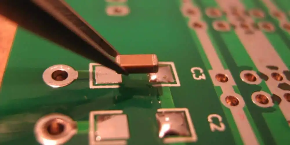
Adding solder pads to an Eagle board layout is a common task in PCB design. This comprehensive guide covers various methods, best practices, and considerations for adding solder pads effectively while maintaining design integrity and manufacturability.

YouTube video

Understanding Solder Pad Types

Common Pad Configurations

Pad TypeCommon UsesTypical Dimensions
Through-holeComponent leads60-100 mil diameter
SMD RectangleSurface mount40×60 mil
SMD OvalFine-pitch ICs20×40 mil
Test PointsDebug/Programming40 mil diameter
Thermal PadsHeat dissipation100+ mil square

Pad Shapes and Properties

ShapeAdvantagesLimitations
RoundEven solder distributionSpace inefficient
RectangleSpace efficientCorner stress
OvalGood wettingComplex geometry
CustomApplication-specificManufacturing challenges

Methods to Add Solder Pads

SMD Pads

Using the PAD Command

StepActionKeyboard Shortcut
1Select PAD commandP
2Choose drill sizeEnter value
3Set pad diameterEnter value
4Place padLeft click
5Rotate if neededR

Using the SMD Command

StepActionKeyboard Shortcut
1Select SMD commandS
2Set dimensionsEnter values
3Choose layerLayer dropdown
4Place padLeft click
5Adjust orientationR

Design Considerations

Pad Size Selection

Component TypeMinimum Pad SizeRecommended Size
0603 SMD20×30 mil30×40 mil
0805 SMD25×35 mil35×45 mil
SOIC Lead20×60 mil25×80 mil
Through-hole60 mil dia80 mil dia

Clearance Requirements

Spacing TypeMinimumRecommended
Pad to Pad6 mil10 mil
Pad to Trace6 mil8 mil
Pad to Via10 mil15 mil
Pad to Board Edge20 mil25 mil

Creating Custom Pad Libraries

Library Development Process

StageTaskConsiderations
PlanningDefine requirementsEnd use case
CreationDraw pad geometryManufacturing limits
TestingVerify design rulesClearances
DocumentationRecord specificationsFuture reference

Package Creation Steps

StepDescriptionKey Points
1Open Library EditorUse correct version
2Create new packageMeaningful name
3Add pads/SMDsFollow standards
4Set propertiesConsider reflow
5Save and verifyRun DRC

Optimization Techniques

Pad Placement Strategies

StrategyBenefitApplication
Grid AlignmentManufacturing easeAll designs
Symmetrical LayoutBetter assemblyMulti-pad components
Thermal ReliefHeat managementPower connections
TeardropMechanical strengthHigh-stress areas

Manufacturing Considerations

FactorRequirementImpact
Minimum Size6 milYield rate
Aspect Ratio1:5 maxManufacturability
Copper Weight1-2 ozSolderability
Surface FinishHASL/ENIGReliability

Advanced Pad Features

Thermal Management

FeaturePurposeWhen to Use
Thermal ReliefHeat controlPower connections
Split PlaneCurrent distributionHigh current
Thermal ViasHeat dissipationHot components

Special Pad Types

TypeUse CaseDesign Notes
Test PointsDebuggingProbe access
Programming PadsDevelopmentHeader spacing
RF PadsSignal integrityImpedance matching
Power PadsCurrent handlingThermal design

DRC and Validation

drc pcb

Design Rule Checks

Rule TypeDefault ValueCustomization
Clearance6 milApplication specific
Annular Ring7 milBased on fab specs
Drill Size12 milThrough-hole needs
Thermal Relief4 spokesPower requirements

Common Issues and Solutions

IssueCauseResolution
DRC ErrorsSpacing violationsAdjust layout
Missing ConnectionsNet assignmentCheck netlist
Thermal ProblemsPoor reliefModify patterns
Manufacturing IssuesSize violationsFollow specs

Layer Management

Layer Assignment

LayerPurposeConsiderations
TopComponent mountingComponent density
BottomSecondary mountingAssembly access
InnerPower distributionCurrent capacity
SilkscreenIdentificationText readability

Mask Settings

SettingFunctionImpact
TentingVia coverageAssembly process
Mask ReliefSolder controlJoint quality
Stop MaskExposure controlSelective soldering
Paste MaskPaste volumeSMT assembly

Frequently Asked Questions (FAQ)

Q1: How do I determine the correct pad size for my component?

A1: Pad size determination involves several factors:

  1. Component manufacturer specifications
  2. Manufacturing capabilities
  3. Assembly requirements
  4. Thermal considerations

General guidelines:

  • Add 20% to manufacturer’s minimum recommendations
  • Consider paste mask reduction for SMD components
  • Account for component tolerances
  • Factor in assembly method (hand vs. machine)

Q2: What’s the difference between through-hole and SMD pads in Eagle?

A2: Key differences include:

  • Through-hole pads (PAD command):
    • Require drill holes
    • Appear on all layers
    • Generally larger
  • SMD pads (SMD command):
    • Single layer only
    • No drill holes
    • Usually smaller
    • More space-efficient

Q3: How can I modify multiple pads simultaneously?

A3: To modify multiple pads:

  1. Use the GROUP command (keyboard shortcut: G)
  2. Select all target pads
  3. Use CHANGE command
  4. Select property to modify
  5. Apply changes to group

Properties that can be changed:

  • Size
  • Shape
  • Orientation
  • Layer assignment

Q4: Why do my pads show DRC errors even though they look correct?

A4: Common causes of DRC errors:

  1. Clearance violations
  2. Minimum size violations
  3. Layer assignment issues
  4. Net connectivity problems

Resolution steps:

  • Check design rules settings
  • Verify pad dimensions
  • Confirm layer assignments
  • Review net assignments

Q5: How do I create custom pad shapes for special requirements?

A5: Custom pad creation process:

  1. Use Library Editor
  2. Create new package
  3. Combine basic shapes:
    • Rectangle SMDs
    • Round pads
    • Polygons
  4. Set appropriate properties
  5. Save to library
  6. Verify manufacturability

Remember:

  • Keep shapes manufacturable
  • Consider paste mask requirements
  • Document custom shapes
  • Verify with manufacturer

How to Solder Flex PCBs โ€“ Step-by-Step Guide for Avoiding Cracks & Failures

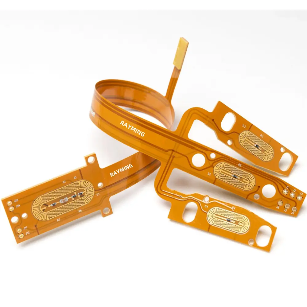
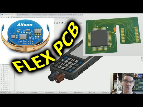
Flexible printed circuit boards (flex PCBs) have revolutionized electronic design by enabling compact, lightweight, and dynamic applications that traditional rigid PCBs cannot support. However, the delicate nature of these flexible circuits presents unique challenges when it comes to soldering. Improper soldering techniques can lead to costly failures including cracks, delamination, and broken connections. This comprehensive guide will walk you through the essentials of properly soldering flex PCBs to ensure durable, reliable connections and avoid common pitfalls that plague even experienced technicians.

Understanding Flex PCBs and Their Unique Properties
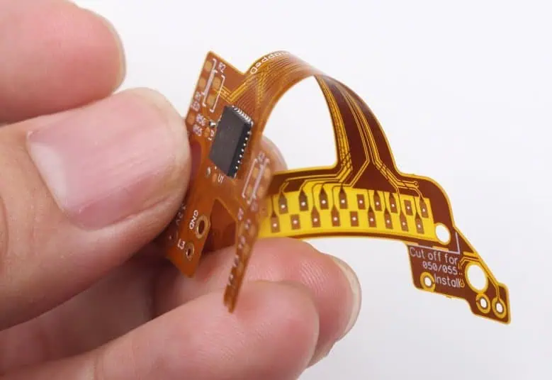
What Is a Flex PCB?

A flex PCB is a printed circuit board manufactured using flexible base materials, typically polyimide (like Kapton) or polyester films, with conductive traces of copper applied to these flexible substrates. Unlike their rigid counterparts, flex PCBs can bend, fold, and twist, making them ideal for applications where space is constrained or movement is required.

Key Differences Between Flex and Rigid PCBs

When comparing flex PCBs to traditional rigid boards, several critical differences impact the soldering process:

  • Material Properties: Flex PCBs use heat-sensitive polymer films that can warp, melt, or delaminate under excessive heat.
  • Thermal Expansion: Flex materials expand and contract at different rates than rigid boards, creating potential stress points during thermal cycling.
  • Thickness: Flex PCBs are significantly thinner (often 0.1mm-0.2mm) than rigid boards, making them more susceptible to heat damage.
  • Copper Flexibility: The copper traces on flex circuits are designed to withstand bending but can develop microcracks when subjected to improper heating during soldering.

Why Soldering Flex PCBs Requires Special Techniques

The unique properties of flex PCBs create specific challenges:

  • Their thin, flexible nature makes them prone to warping under heat
  • The thermal sensitivity of the base materials requires precise temperature control
  • The dimensional instability during heating can cause misalignment of components
  • Mechanical stress during handling can compound thermal stress from soldering

Understanding these fundamental differences is essential before attempting to solder flex PCBs. With this knowledge in mind, let’s explore the tools and materials you’ll need for successful flex PCB soldering.

Essential Tools and Materials for Flex PCB Soldering

Specialized Soldering Equipment

For optimal results when soldering flex PCBs, consider investing in:

  • Temperature-controlled soldering iron: Look for models with digital temperature displays and quick recovery times
  • Fine-tipped soldering tips: Precision tips (0.5mm or smaller) allow for accurate work on delicate traces
  • Hot air rework station: For SMD components and areas requiring controlled, distributed heat
  • Preheating platform: Helps minimize thermal shock and reduces the temperature differential during soldering

Recommended Solder Types and Flux

The right consumables make a significant difference:

  • Low-temperature solder: SAC305 (96.5% tin, 3% silver, 0.5% copper) or similar lead-free alloys with melting points around 217ยฐC
  • Fine-gauge solder wire: 0.5mm or thinner diameter wire for precision work
  • No-clean flux: Specifically formulated for flexible circuits with minimal residue
  • Liquid flux pen: For precise application to small areas
  • Flux remover: Compatible with polyimide and other flex substrates

Workstation Setup for Success

Proper preparation of your workspace helps prevent damage:

  • ESD-safe environment: Anti-static mats, wrist straps, and ionizers to prevent electrostatic discharge
  • Magnification: Illuminated magnifiers or microscopes (10-30x) for precision inspection
  • Supporting fixtures: Non-conductive materials to support the flex during soldering
  • Proper lighting: Shadow-free, adjustable lighting to clearly see small components
  • Thermal management tools: Heat sinks or heat-resistant tape to protect sensitive areas

With your equipment prepared, the next step is understanding how to properly handle and prepare flex PCBs before soldering begins.

Preparing for Soldering: Handling and Inspection

Safe Handling Techniques for Flex PCBs

Improper handling before soldering even begins can damage flex circuits:

  • Always support the entire flex PCB during handling to prevent bending in unintended areas
  • Use clean, lint-free gloves to prevent oils and contaminants from affecting solder adhesion
  • Avoid creasing or folding the flex material beyond its specified bend radius
  • Transport and store flex PCBs flat or on curved surfaces matching their intended configuration
  • Minimize the number of flex operations before soldering to prevent fatigue stress

Surface Preparation and Cleaning

Proper cleaning is critical for successful soldering:

  • Use isopropyl alcohol (90%+ concentration) and lint-free wipes to remove oils and contaminants
  • Allow the flex PCB to completely dry before soldering to prevent trapped moisture
  • Avoid abrasive cleaning methods that could damage the thin copper traces
  • For oxidized pads, use a specialized PCB cleaner designed for flex materials
  • Inspect the cleaned surface under magnification to ensure all residues are removed

Pre-Soldering Inspection Checklist

Before applying heat, verify:

  • All components match the design specifications for flex applications
  • The flex circuit shows no signs of damage, delamination, or scratched traces
  • Pads and traces are free from oxidation and contaminants
  • The circuit is properly supported to prevent movement during soldering
  • Temperature settings on equipment are appropriate for the specific flex material
  • Test components are correctly oriented and positioned

With proper preparation complete, you’re ready to begin the actual soldering process.

Step-by-Step Guide to Soldering Flex PCBs

Step 1: Preheat the Flex PCB (When Necessary)

Preheating is often essential for flex PCB soldering:

  • Why preheating matters: It reduces thermal shock, minimizes warping, and improves solder flow
  • Safe temperature ranges: Typically 80-120ยฐC, always below the glass transition temperature of the flex material
  • Preheating methods:
    • Use a dedicated preheating platform set to the appropriate temperature
    • Allow gradual warming for 2-3 minutes before soldering
    • Monitor the temperature with a non-contact infrared thermometer
    • Ensure even heating across the entire flex PCB

Step 2: Position and Secure Components

Proper positioning prevents stress during soldering:

  • Use heat-resistant tape or specialized fixtures to hold components in place
  • Support the flex material completely to prevent unintended bending during heating
  • For double-sided assemblies, secure components on one side before soldering the other
  • Ensure components sit flat and are properly aligned with pads
  • Avoid placing excessive pressure on the flex material when securing components

Step 3: Apply Flux Correctly

Flux application is critical for clean, strong joints:

  • Apply a small amount of no-clean flux to the pads using a precision applicator
  • Avoid excess flux that could spread to unwanted areas or be difficult to remove
  • For sensitive areas, use a flux pen to target specific pads
  • Remember that flex circuits often require more flux than rigid boards due to their thermal properties
  • Allow the flux to activate briefly before applying solder

Step 4: Solder with Precision and Speed

The actual soldering process requires careful technique:

  • For hand soldering:
    • Set your soldering iron to the lowest effective temperature (typically 260-290ยฐC)
    • Touch both the pad and component lead simultaneously
    • Apply solder to the junction of the tip, pad, and component
    • Complete each joint quickly (1-2 seconds of contact)
    • Move methodically to distribute heat evenly across the flex circuit
  • For reflow soldering:
    • Use a gentler temperature profile than for rigid PCBs
    • Extend the preheat phase to allow for gradual temperature increase
    • Reduce the peak temperature by 5-10ยฐC compared to rigid board profiles
    • Ensure cooling is controlled and gradual
  • For hot bar soldering:
    • Use dedicated flex-compatible hot bar equipment
    • Apply uniform pressure across the connection
    • Minimize dwell time to prevent overheating

Step 5: Inspect Solder Joints Thoroughly

Quality inspection prevents failures:

  • Use magnification to examine each joint for proper wetting and formation
  • A good solder joint on a flex PCB should be smooth, concave, and bright
  • Look for signs of overheating such as discoloration of the substrate
  • Check for cold joints, which appear dull and rough
  • Verify no solder bridges exist between adjacent pads
  • Ensure there is no evidence of damaged or lifted pads

Read more about:

Advanced Tips for Preventing Cracks and Failures

Managing Thermal Stress

Thermal management is crucial for flex PCB durability:

  • Allow the assembly to cool naturally; never force cool with compressed air
  • Use heat sinks to protect sensitive components and areas
  • Consider staggered soldering patterns to distribute heat more evenly
  • Allow cooling periods between soldering multiple joints in close proximity
  • For complex assemblies, solder in zones moving from the center outward

Mechanical Support Techniques

Proper support prevents mechanical damage:

  • Use silicone or Kapton tape to create strain relief at transition points between rigid and flex areas
  • Apply conformal coating to provide additional support and protection
  • Consider stiffeners in high-stress areas where components are mounted
  • Design soldering fixtures that support the natural contours of the flex circuit
  • Avoid creating sharp bends near solder joints

Protective Measures for Long-Term Reliability

Post-soldering protection extends service life:

  • Apply appropriate conformal coatings compatible with flex materials
  • Use strain relief features at connection points and transition zones
  • Consider encapsulation for high-reliability applications
  • Implement underfill for larger components to distribute mechanical stress
  • Design cases or enclosures that prevent excessive bending at solder joints

Common Mistakes and Troubleshooting

Overheating the Flex Material

Signs and solutions for heat damage:

  • Symptoms: Discoloration, bubbling, or delamination of the flex material
  • Prevention: Use lower temperatures and shorter contact times
  • Solution: For minor damage, inspect for electrical continuity; for severe cases, the affected section may need replacement

Excessive Mechanical Stress

Managing physical damage:

  • Symptoms: Cracked solder joints, lifted pads, or broken traces
  • Prevention: Proper support during soldering and handling
  • Solution: Repair damaged traces with conductive epoxy; use reinforcement patches for structural integrity

Using Inappropriate Solder or Flux

Material compatibility issues:

  • Symptoms: Poor wetting, cold joints, or excessive residue
  • Prevention: Use only flex-compatible, low-temperature solders and fluxes
  • Solution: Remove improper solder completely and reapply correct materials

Advanced Techniques for Complex Flex PCB Assemblies

Laser Soldering for High-Precision Applications

When ultimate precision is required:

  • Laser soldering provides extremely controlled heat application
  • Ideal for densely populated flex circuits
  • Minimizes heat-affected zones around delicate areas
  • Especially useful for medical and aerospace applications
  • Requires specialized equipment and training

Heat Staking Methods

For securing components mechanically:

  • Heat stakes create mechanical bonds in addition to electrical connections
  • Provides additional support for components on flex circuits
  • Reduces reliance on solder joint strength alone
  • Particularly useful for high-vibration environments
  • Can be combined with traditional soldering for maximum reliability

Adhesive Reinforcement Strategies

Combining adhesives with solder:

  • Use specialized conductive adhesives for extremely heat-sensitive areas
  • Apply non-conductive structural adhesives around large components for support
  • Consider “dot and fill” techniques where adhesive dots secure components before soldering
  • Implement underfill for larger components to distribute mechanical stress
  • Use edge bonding to further secure components against shock and vibration

Conclusion: Mastering the Art of Flex PCB Soldering

Soldering flex PCBs successfully requires understanding their unique properties and adapting techniques accordingly. By following the guidelines in this comprehensive guide, you can avoid the common pitfalls of cracked joints, delamination, and thermal damage that often plague flexible circuit assemblies.

Remember that patience and precision are your greatest allies when working with these delicate yet powerful components. Proper equipment, careful temperature control, and meticulous attention to detail will result in reliable, long-lasting connections that maintain the integrity of your flex PCB designs.

As flexible electronics continue to expand into new applications from wearable technology to automotive systems, mastering these specialized soldering techniques will become an increasingly valuable skill for electronics professionals.

FAQs About Soldering Flex PCBs

Can you use regular soldering irons on flex PCBs?

Yes, but only with temperature-controlled models set to appropriate temperatures (typically 260-290ยฐC). Standard unregulated irons often run too hot and can damage flex materials.

What temperature should I use for soldering flex circuits?

The optimal temperature depends on the specific flex material, but generally, 260-290ยฐC for hand soldering is recommended. Always use the lowest effective temperature that creates good solder flow.

How do you prevent flex PCB warping during soldering?

Prevent warping by using proper support fixtures, applying preheating techniques, distributing heat evenly across the circuit, and allowing natural, gradual cooling after soldering.

Is it necessary to use special solder for flex PCBs?

While not always mandatory, low-temperature solders (melting around 217ยฐC) are strongly recommended to minimize thermal stress on the flexible substrate.

How can I repair a cracked trace on a flex PCB?

Small cracks can be repaired using conductive epoxy or by carefully soldering a fine wire jumper across the damaged area. For critical applications, consider replacing the affected section.

What’s the best way to clean flux residue from flex PCBs?

Use isopropyl alcohol (90%+ concentration) with lint-free wipes, or specialized flex-compatible flux removers. Avoid aggressive solvents that could damage the flex material.

What Does a Filter Capacitor Do?

Filter capacitors are essential components in electronic circuits, playing a crucial role in maintaining stable power supply and signal integrity. This comprehensive guide explores the functions, types, applications, and best practices for using filter capacitors in various electronic designs.

YouTube video

Basic Principles of Filter Capacitors

Fundamental Operation

AspectDescriptionImpact
Energy StorageTemporary charge storageVoltage stabilization
ImpedanceFrequency-dependent resistanceSignal filtering
Response TimeMicroseconds to millisecondsRipple reduction
Current FlowAC current passes, DC blockedNoise elimination

Types of Filtering Actions

Filter TypePrimary FunctionCommon Applications
Low-passBlocks high frequenciesPower supplies
High-passBlocks low frequenciesAudio coupling
Band-passSelects frequency rangeRadio circuits
NotchBlocks specific frequenciesNoise elimination

Types of Filter Capacitors

Electrolytic Capacitors

ParameterRangeApplications
Capacity0.1 ยตF to 100,000 ยตFPower filtering
Voltage6.3V to 450VSupply smoothing
ESR0.01ฮฉ to 1ฮฉRipple control
Lifetime2,000 to 10,000 hoursLong-term stability

Ceramic Capacitors

TypeCharacteristicsBest Use
Class 1Stable, low capacityHigh-frequency
Class 2Higher capacity, less stableGeneral purpose
Class 3Highest capacity, least stableBulk filtering

Film Capacitors

MaterialPropertiesApplications
PolyesterGood stabilityDC blocking
PolypropyleneLow lossAC filtering
MetallizedSelf-healingHigh voltage

Applications in Power Supply Filtering

Input Filtering

StageCapacitor TypePurpose
Bridge RectifierElectrolyticBulk filtering
Input ProtectionCeramicTransient suppression
EMI PreventionFilmNoise reduction

Output Filtering

ParameterSpecificationImpact
Ripple Voltage<1% of DC outputLoad stability
Response Time<100 ยตsTransient response
ESR<0.1ฮฉEfficiency
Temperature Rise<20ยฐCReliability

Design Considerations

Capacitor Selection Criteria

FactorConsiderationImportance
Voltage Rating1.5x operating voltageSafety margin
CapacitanceBased on ripple currentPerformance
ESRApplication dependentEfficiency
Temperature RangeOperating environmentReliability

Common Design Mistakes

ErrorImpactSolution
Undersized CapacityHigh rippleIncrease capacitance
Excessive ESRHeat generationBetter quality parts
Wrong typePoor performanceProper selection
Inadequate voltage ratingEarly failureHigher rating

Performance Optimization

Ripple Reduction Techniques

MethodEffectivenessTrade-offs
Parallel capacitorsVery goodCost, space
Series configurationGoodVoltage sharing
Multiple stage filteringExcellentComplexity
Active filteringBestCost, complexity

Temperature Considerations

Temperature RangeImpactMitigation
-40ยฐC to 0ยฐCReduced capacityOversize rating
0ยฐC to 50ยฐCOptimal rangeStandard design
50ยฐC to 85ยฐCReduced lifetimeCooling needed
>85ยฐCRapid degradationRedesign required

Advanced Applications

High-Frequency Filtering

Frequency RangeCapacitor TypeDesign Notes
100 kHz – 1 MHzCeramicLow inductance
1 MHz – 10 MHzSpecial ceramicLayout critical
>10 MHzRF ceramicSpecial layout

Power Supply Decoupling

Circuit TypeCapacitor ValuePlacement
Digital IC0.1 ยตFClose to pins
Analog IC10 ยตFWithin 5mm
Power IC100 ยตFMultiple caps

Reliability and Lifetime

Failure Modes

ModeCausePrevention
Short CircuitOvervoltageProper rating
Open CircuitPhysical damageProtection
Parameter DriftAgingRegular maintenance
Thermal RunawayOverloadThermal design

Lifetime Factors

FactorImpactManagement
Temperature-50% per 10ยฐC riseCooling
Voltage StressExponential effectDerating
Ripple CurrentLinear effectProper sizing
EnvironmentVariableProtection

Cost-Effectiveness

Cost vs. Performance

GradeCost FactorApplication
Consumer1xNon-critical
Industrial2-3xProfessional
Military5-10xCritical
Space20x+Aerospace

Value Engineering

StrategySavingsRisk
Parallel smaller caps10-20%More parts
Alternative materials15-30%Performance
Optimized ratings5-15%Margin
Volume purchasing20-40%Inventory

Frequently Asked Questions (FAQ)

Q1: How do I calculate the required capacitance for power supply filtering?

A1: The required capacitance can be calculated using the formula: C = (I ร— t) / ฮ”V Where:

  • I = Load current (A)
  • t = Time between peaks (s)
  • ฮ”V = Acceptable ripple voltage (V) For most applications, add 20-30% margin to the calculated value.

Q2: Why do filter capacitors fail, and how can I prevent failures?

A2: Filter capacitors typically fail due to:

  • Excessive voltage stress
  • High operating temperature
  • Ripple current overload
  • Age-related degradation Prevention involves:
  1. Using appropriate voltage ratings (1.5x operating voltage)
  2. Ensuring proper thermal management
  3. Regular maintenance and inspection
  4. Proper circuit design with safety margins

Q3: What’s the difference between using multiple small capacitors versus one large capacitor?

A3: Multiple small capacitors often provide better performance because:

  • Lower equivalent ESR
  • Better high-frequency response
  • Improved thermal distribution
  • Enhanced reliability through redundancy However, this approach requires more board space and can increase assembly costs.

Q4: How often should filter capacitors be replaced in power supplies?

A4: Replacement intervals depend on:

  • Operating conditions
  • Capacitor quality
  • Environmental factors
  • Application criticality

Typical guidelines:

  • Consumer equipment: 5-7 years
  • Industrial equipment: 7-10 years
  • Critical systems: Based on regular testing
  • High-reliability: Preventive replacement at 50% of rated life

Q5: Can I mix different types of filter capacitors in the same circuit?

A5: Yes, mixing capacitor types can be beneficial:

  • Electrolytics for bulk filtering
  • Ceramics for high-frequency noise
  • Film capacitors for intermediate frequencies

Best practices:

  1. Place high-frequency filters closest to the source
  2. Use appropriate values for each frequency range
  3. Consider impedance characteristics
  4. Ensure proper layout for effective filtering

What are the disadvantages of flexible PCBs?

Flexible Printed Circuit Boards (PCBs) have revolutionized the electronics industry, offering numerous advantages such as reduced weight, space savings, and improved reliability. However, like any technology, they also come with their own set of drawbacks. This article delves into the various disadvantages of flexible PCBs, providing a comprehensive overview of the challenges faced by manufacturers, designers, and end-users when working with this technology.

Understanding Flexible PCBs

Before we explore the disadvantages, let’s briefly recap what flexible PCBs are and their basic characteristics.

Definition and Basic Characteristics

Flexible PCBs, also known as flex circuits, are electronic circuits mounted on flexible substrate materials. Unlike rigid PCBs, these circuits can bend, fold, and conform to various shapes, making them ideal for applications where space is at a premium or where the circuit needs to flex during use.

YouTube video

Key Components

The typical components of a flexible PCB include:

  1. Flexible substrate (usually polyimide or polyester)
  2. Conductive layers (typically copper)
  3. Coverlay or cover coat
  4. Adhesives
  5. Stiffeners (in some designs)

Now that we have a basic understanding, let’s explore the disadvantages of flexible PCBs.

Learn more about:

  1. Flex PCB Stackupย 
  2. Flex PCB Stiffener
  3. Flex PCB Assembly
  4. 6 Layer Flex PCB
  5. 8 Layer Flex PCB

Cost Considerations

Higher Initial Costs

One of the most significant disadvantages of flexible PCBs is their higher initial cost compared to rigid PCBs.

Table 1: Cost Comparison – Flexible vs. Rigid PCBs

FactorFlexible PCBsRigid PCBs
Raw Material CostHigherLower
Manufacturing ComplexityHigherLower
Specialized EquipmentRequiredStandard
Design TimeLongerShorter
Overall Initial CostHigherLower

The higher costs associated with flexible PCBs stem from several factors:

  1. Expensive raw materials: The polyimide or polyester substrates used in flexible PCBs are more expensive than the FR-4 material commonly used in rigid PCBs.
  2. Complex manufacturing process: Producing flexible PCBs requires specialized equipment and more intricate processes, increasing production costs.
  3. Design complexity: Designing flexible PCBs often takes more time and expertise, adding to the overall cost.

Limited Cost-Effectiveness for Low-Volume Production

While flexible PCBs can be cost-effective for high-volume production, they may not be economically viable for low-volume or prototype runs.

Design and Manufacturing Challenges

Complex Design Process

Designing flexible PCBs presents unique challenges that can be time-consuming and require specialized expertise.

Bend Radius Considerations

One of the critical aspects of flexible PCB design is accounting for the bend radius. Designers must ensure that the circuit can flex without damaging the conductive traces or components.

Table 2: Typical Minimum Bend Radii for Flexible PCBs

Number of LayersMinimum Bend Radius (mm)
Single-sided0.8 – 1.5
Double-sided1.5 – 2.5
Multilayer3.0 – 6.0

Limited Layer Count

Flexible PCBs typically have fewer layers than their rigid counterparts, which can limit circuit complexity and functionality.

Table 3: Typical Layer Count Comparison

PCB TypeTypical Maximum Layers
Flexible PCBs4-6
Rigid PCBs16-32 (or more)

This limitation can force designers to make trade-offs between flexibility and circuit complexity.

Manufacturing Challenges

Handling and Processing Difficulties

The flexible nature of these PCBs can make them more challenging to handle during the manufacturing process. Issues such as warping, twisting, or folding can occur, potentially leading to defects or reduced yield rates.

Specialized Equipment Requirements

Manufacturing flexible PCBs requires specialized equipment, which can be a significant investment for PCB fabricators. This requirement can limit the number of manufacturers capable of producing flexible PCBs, potentially affecting lead times and costs.

Performance and Reliability Concerns

Thermal Management Issues

Flexible PCBs face unique challenges when it comes to heat dissipation.

Limited Heat Dissipation

The thin, flexible nature of these PCBs means they have less mass to absorb and dissipate heat compared to rigid PCBs. This can lead to potential overheating issues, especially in high-power applications.

Table 4: Thermal Conductivity Comparison

MaterialThermal Conductivity (W/mK)
FR-4 (typical rigid PCB)0.3 – 0.8
Polyimide (typical flex PCB)0.12 – 0.46
Copper (for reference)385

Mechanical Stress and Fatigue

While flexibility is a key advantage of these PCBs, it also introduces potential reliability issues.

Repeated Flexing

In applications where the PCB needs to flex repeatedly, there’s a risk of mechanical fatigue. This can lead to cracked traces, delamination, or component failure over time.

Table 5: Flex Life of Different Flexible PCB Constructions

Construction TypeTypical Flex Life (number of flexes)
Single-layer1,000,000+
Double-layer100,000 – 500,000
Multilayer10,000 – 100,000

Environmental Sensitivity

Flexible PCBs can be more sensitive to environmental factors compared to rigid PCBs.

Moisture Sensitivity

The polyimide material commonly used in flexible PCBs can absorb moisture, potentially leading to delamination or changes in electrical properties.

Temperature Extremes

While flexible PCBs can generally withstand a wide range of temperatures, extreme conditions can cause issues such as dimensional changes or adhesive degradation.

Limited Repairability and Modification

Difficulty in Rework and Repair

Flexible PCBs present unique challenges when it comes to rework and repair.

Delicate Nature

The thin, flexible structure of these PCBs makes them more susceptible to damage during rework attempts. Standard repair techniques used for rigid PCBs may not be suitable or may risk further damage.

Limited Access

In applications where the flexible PCB is tightly integrated into a product, accessing the PCB for repairs can be extremely difficult or impossible without disassembling the entire product.

Challenges in Post-Production Modifications

Making changes to a flexible PCB after production can be more challenging compared to rigid PCBs.

Limited Real Estate

The compact nature of flexible PCB designs often means there’s little to no extra space for additional components or traces, making modifications difficult.

Maintaining Flexibility

Any modifications must be carefully considered to ensure they don’t compromise the PCB’s ability to flex as required in the application.

Component and Assembly Limitations

Restricted Component Selection

Not all electronic components are suitable for use with flexible PCBs.

Size and Weight Constraints

Larger or heavier components may not be suitable for flexible PCBs as they can create stress points and limit flexibility.

Table 6: Component Suitability for Flexible PCBs

Component TypeSuitabilityReason
SMD (small)ExcellentLow profile, lightweight
SMD (large)FairMay limit flexibility
Through-holePoorCan create stress points, limit flexibility
Ball Grid Array (BGA)GoodDepends on size and pitch

Assembly Challenges

Prototype Assembling components onto flexible PCBs can be more challenging than with rigid PCBs.

Specialized Equipment

Standard pick-and-place machines may struggle with the flexible nature of the PCB, requiring specialized equipment or processes.

Soldering Difficulties

The heat-sensitive nature of flexible substrates can make soldering more challenging, requiring precise temperature control to avoid damaging the PCB.

Regulatory and Compliance Issues

EMI/EMC Challenges

Flexible PCBs can face unique challenges in meeting electromagnetic interference (EMI) and electromagnetic compatibility (EMC) requirements.

Limited Shielding Options

The thin, flexible nature of these PCBs can make it more difficult to incorporate effective EMI shielding compared to rigid PCBs.

Signal Integrity Issues

The flexible structure can potentially lead to signal integrity issues, especially in high-frequency applications, making it more challenging to meet EMC standards.

Environmental Compliance

While flexible PCBs themselves are often compliant with environmental regulations, the overall product may face challenges.

End-of-Life Considerations

The integrated nature of flexible PCBs in some applications can make them more difficult to separate and recycle at the end of a product’s life, potentially impacting compliance with e-waste regulations.

Conclusion

While flexible PCBs offer numerous advantages and have enabled many innovative product designs, it’s crucial to consider their disadvantages when deciding whether to use them in a particular application. From higher costs and design complexities to performance limitations and regulatory challenges, flexible PCBs present a unique set of trade-offs.

By understanding these disadvantages, engineers and product designers can make informed decisions about when and how to use flexible PCBs, balancing their benefits against their drawbacks to create optimal solutions for their specific applications.

Frequently Asked Questions (FAQ)

Q1: Are flexible PCBs more expensive than rigid PCBs?

A1: Yes, flexible PCBs typically have higher initial costs than rigid PCBs due to more expensive raw materials, complex manufacturing processes, and specialized design requirements. However, they can be cost-effective in high-volume production or where their unique properties provide significant advantages.

Q2: Can flexible PCBs handle high-power applications?

A2: Flexible PCBs generally have more limited heat dissipation capabilities compared to rigid PCBs, which can make them less suitable for high-power applications. However, design techniques such as using thicker copper layers or incorporating thermal management solutions can help mitigate this limitation in some cases.

Q3: How many times can a flexible PCB be bent?

A3: The number of times a flexible PCB can be bent depends on factors such as the PCB’s construction, the bend radius, and the specific materials used. Single-layer flex PCBs can often withstand over a million flexes, while multilayer designs may be limited to tens or hundreds of thousands of flexes.

Q4: Are all components compatible with flexible PCBs?

A4: Not all components are suitable for use with flexible PCBs. Small surface-mount devices (SMDs) are generally the most compatible, while larger or heavier components may be problematic. Through-hole components are typically avoided in flexible PCB designs as they can create stress points and limit flexibility.

Q5: Can flexible PCBs be repaired easily?

A5: Repairing flexible PCBs is generally more challenging than repairing rigid PCBs. Their delicate nature and often tightly integrated designs can make access difficult and increase the risk of damage during repair attempts. In many cases, it may be more practical to replace the entire flexible PCB rather than attempt a repair.

Express PCB And Express SCH Designing Software

Express PCB and Express SCH represent a powerful combination of circuit design tools that have become popular among electronics engineers, hobbyists, and professional designers. This comprehensive guide explores both software packages, their features, capabilities, and how they work together to streamline the electronic design process.

YouTube video

Express SCH Overview

Core Features and Capabilities

Feature CategoryDescriptionBenefits
Component LibraryOver 10,000 built-in componentsQuick start for common designs
Custom ComponentsUser-defined symbol creationFlexibility for specialized needs
Net LabelsAutomated connectivity trackingReduces wiring errors
Multi-page SupportUp to 100 pages per designHandles complex projects
Export OptionsPDF, PNG, BMP formatsEasy documentation

User Interface Elements

UI ElementFunctionAccess Method
Component BrowserBrowse and select partsLeft sidebar
Properties PanelEdit component parametersRight-click menu
Drawing ToolsCreate custom symbolsTop toolbar
Sheet NavigatorSwitch between pagesBottom panel
Net ManagerView and edit connectionsTools menu

Express PCB Features

Board Design Capabilities

FeatureSpecificationLimitations
Maximum Board Size31″ x 31″Single-sided view
Layer SupportUp to 4 layersNo blind/buried vias
Minimum Trace Width6 milManufacturing dependent
Grid Resolution0.001 inchFixed metric conversion
Component Spacing0.025 inch minimumDRC recommended

Manufacturing Specifications

ParameterStandard OptionPremium Option
Copper Weight1 oz2 oz available
Minimum Hole Size0.020″0.013″
SilkscreenBoth sidesHigh resolution
Solder MaskGreen standardMultiple colors
Turn-around Time3-5 days24-hour available

Integration Between Express SCH and PCB

Data Transfer Workflow

StepProcessVerification
Schematic CompleteDesign verificationDRC check
Component AssociationLink SCH to PCB footprintsLibrary check
Net List GenerationAutomatic creationConnectivity review
PCB ImportComponent placementLayout verification
Final CheckDesign rule verificationManufacturing review

Design Process Best Practices

Project Setup Guidelines

Schematic Design Phase

TaskRecommendationCommon Pitfalls
Page SetupStart with main sheetInconsistent sheet sizes
Component SelectionUse standard parts firstCustom part errors
Power DistributionDefine earlyGround loop issues
Signal RoutingGroup similar signalsNoise coupling
DocumentationAdd notes during designMissing information

PCB Layout Phase

StageFocus AreasQuality Checks
Component PlacementPower flow optimizationThermal considerations
Layer StackSignal integrityImpedance control
Routing StrategyCritical paths firstDRC compliance
Thermal ManagementHeat dissipationComponent spacing
Manufacturing ReviewDFM guidelinesCost optimization

Advanced Features and Techniques

Custom Library Development

Element TypeCreation MethodVerification Steps
Schematic SymbolsVector drawing toolsPin mapping check
PCB FootprintsDimension inputPad spacing review
Combined DevicesLibrary linkingAssociation test
Custom Packages3D modeling supportManufacturing check

Design Rule Implementation

Rule CategoryParametersVerification Method
ClearanceTrace-to-trace spacingDRC check
Hole SizeDrill specificationsManufacturing limits
Copper WidthCurrent capacityThermal analysis
Layer RulesStack-up requirementsSignal integrity

Performance Optimization

System Requirements

ComponentMinimumRecommended
Processor1.5 GHz3+ GHz
RAM4 GB8+ GB
Storage500 MB2+ GB
Display1366×7681920×1080
OS SupportWindows 7Windows 10/11

Software Performance Tips

AreaOptimizationImpact
File ManagementRegular savingData protection
Memory UsageBackground appsSpeed improvement
GraphicsHardware accelerationSmooth rendering
BackupAutomated backupsDesign security

Cost Considerations

Licensing Options

License TypeFeaturesPrice Range
BasicEssential toolsFree
StandardFull feature set$100-200
ProfessionalAdvanced capabilities$200-500
EnterpriseMulti-user supportCustom

Manufacturing Cost Factors

FactorImpactOptimization
Board SizeDirect cost correlationEfficient layout
Layer CountExponential cost increaseLayer optimization
Component DensityAssembly complexityStrategic placement
Special RequirementsAdditional processingDesign alternatives

Future Development and Updates

Planned Features

Feature CategoryExpected ImplementationBenefits
Cloud IntegrationNext major releaseRemote collaboration
AI Assisted RoutingDevelopment phaseLayout optimization
3D VisualizationBeta testingDesign verification
Advanced DRCUpcoming updateError reduction

Frequently Asked Questions (FAQ)

Q1: Can Express PCB and Express SCH files be exported to other CAD software?

A1: Express PCB and Express SCH use proprietary file formats, but they offer limited export capabilities. Schematics can be exported as PDF or image files, while PCB designs can be exported as Gerber files for manufacturing. However, direct conversion to other CAD formats is not supported.

Q2: What are the limitations of the free version compared to the paid versions?

A2: The free version includes basic schematic and PCB design capabilities but has limitations on:

  • Board size (maximum 4″ x 4″)
  • Layer count (2 layers maximum)
  • Export options (limited file formats)
  • Advanced features (no auto-routing or DRC) Paid versions remove these restrictions and add professional features.

Q3: How does the auto-routing capability compare to other PCB design software?

A3: Express PCB’s auto-routing functionality is basic compared to professional tools like Altium or KiCad. It works well for simple designs but may struggle with:

  • High-density boards
  • Complex routing rules
  • Mixed-signal designs Manual routing is recommended for critical signals and complex layouts.

Q4: Can I create custom component libraries in Express SCH and PCB?

A4: Yes, both Express SCH and PCB support custom component creation. The process involves:

  1. Creating the schematic symbol in Express SCH
  2. Designing the PCB footprint in Express PCB
  3. Linking the components through the library manager
  4. Validating the new component in test designs

Q5: How reliable is the integration between Express SCH and PCB?

A5: The integration between Express SCH and PCB is generally reliable for basic to moderate complexity designs. Key considerations include:

  • Component associations must be properly defined
  • Net names must be consistent
  • Manual verification of the transfer is recommended
  • Complex designs may require additional checking Regular saving and backup of both files is recommended during the transfer process.