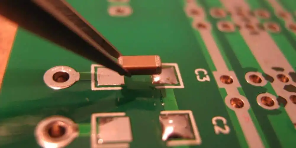
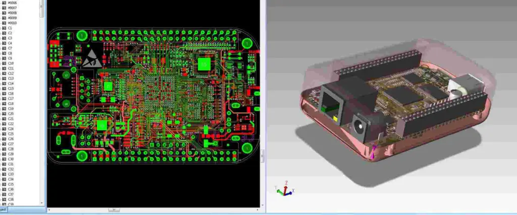
Adding solder pads to an Eagle board layout is a common task in PCB design. This comprehensive guide covers various methods, best practices, and considerations for adding solder pads effectively while maintaining design integrity and manufacturability.

Understanding Solder Pad Types
Common Pad Configurations
| Pad Type | Common Uses | Typical Dimensions |
| Through-hole | Component leads | 60-100 mil diameter |
| SMD Rectangle | Surface mount | 40×60 mil |
| SMD Oval | Fine-pitch ICs | 20×40 mil |
| Test Points | Debug/Programming | 40 mil diameter |
| Thermal Pads | Heat dissipation | 100+ mil square |
Pad Shapes and Properties
| Shape | Advantages | Limitations |
| Round | Even solder distribution | Space inefficient |
| Rectangle | Space efficient | Corner stress |
| Oval | Good wetting | Complex geometry |
| Custom | Application-specific | Manufacturing challenges |
Methods to Add Solder Pads

Using the PAD Command
| Step | Action | Keyboard Shortcut |
| 1 | Select PAD command | P |
| 2 | Choose drill size | Enter value |
| 3 | Set pad diameter | Enter value |
| 4 | Place pad | Left click |
| 5 | Rotate if needed | R |
Using the SMD Command
| Step | Action | Keyboard Shortcut |
| 1 | Select SMD command | S |
| 2 | Set dimensions | Enter values |
| 3 | Choose layer | Layer dropdown |
| 4 | Place pad | Left click |
| 5 | Adjust orientation | R |
Design Considerations
Pad Size Selection
| Component Type | Minimum Pad Size | Recommended Size |
| 0603 SMD | 20×30 mil | 30×40 mil |
| 0805 SMD | 25×35 mil | 35×45 mil |
| SOIC Lead | 20×60 mil | 25×80 mil |
| Through-hole | 60 mil dia | 80 mil dia |
Clearance Requirements
| Spacing Type | Minimum | Recommended |
| Pad to Pad | 6 mil | 10 mil |
| Pad to Trace | 6 mil | 8 mil |
| Pad to Via | 10 mil | 15 mil |
| Pad to Board Edge | 20 mil | 25 mil |
Creating Custom Pad Libraries
Library Development Process
| Stage | Task | Considerations |
| Planning | Define requirements | End use case |
| Creation | Draw pad geometry | Manufacturing limits |
| Testing | Verify design rules | Clearances |
| Documentation | Record specifications | Future reference |
Package Creation Steps
| Step | Description | Key Points |
| 1 | Open Library Editor | Use correct version |
| 2 | Create new package | Meaningful name |
| 3 | Add pads/SMDs | Follow standards |
| 4 | Set properties | Consider reflow |
| 5 | Save and verify | Run DRC |
Optimization Techniques
Pad Placement Strategies
| Strategy | Benefit | Application |
| Grid Alignment | Manufacturing ease | All designs |
| Symmetrical Layout | Better assembly | Multi-pad components |
| Thermal Relief | Heat management | Power connections |
| Teardrop | Mechanical strength | High-stress areas |
Manufacturing Considerations
| Factor | Requirement | Impact |
| Minimum Size | 6 mil | Yield rate |
| Aspect Ratio | 1:5 max | Manufacturability |
| Copper Weight | 1-2 oz | Solderability |
| Surface Finish | HASL/ENIG | Reliability |
Advanced Pad Features
Thermal Management
| Feature | Purpose | When to Use |
| Thermal Relief | Heat control | Power connections |
| Split Plane | Current distribution | High current |
| Thermal Vias | Heat dissipation | Hot components |
Special Pad Types
| Type | Use Case | Design Notes |
| Test Points | Debugging | Probe access |
| Programming Pads | Development | Header spacing |
| RF Pads | Signal integrity | Impedance matching |
| Power Pads | Current handling | Thermal design |
DRC and Validation

Design Rule Checks
| Rule Type | Default Value | Customization |
| Clearance | 6 mil | Application specific |
| Annular Ring | 7 mil | Based on fab specs |
| Drill Size | 12 mil | Through-hole needs |
| Thermal Relief | 4 spokes | Power requirements |
Common Issues and Solutions
| Issue | Cause | Resolution |
| DRC Errors | Spacing violations | Adjust layout |
| Missing Connections | Net assignment | Check netlist |
| Thermal Problems | Poor relief | Modify patterns |
| Manufacturing Issues | Size violations | Follow specs |
Layer Management
Layer Assignment
| Layer | Purpose | Considerations |
| Top | Component mounting | Component density |
| Bottom | Secondary mounting | Assembly access |
| Inner | Power distribution | Current capacity |
| Silkscreen | Identification | Text readability |
Mask Settings
| Setting | Function | Impact |
| Tenting | Via coverage | Assembly process |
| Mask Relief | Solder control | Joint quality |
| Stop Mask | Exposure control | Selective soldering |
| Paste Mask | Paste volume | SMT assembly |
Frequently Asked Questions (FAQ)
Q1: How do I determine the correct pad size for my component?
A1: Pad size determination involves several factors:
- Component manufacturer specifications
- Manufacturing capabilities
- Assembly requirements
- Thermal considerations
General guidelines:
- Add 20% to manufacturer’s minimum recommendations
- Consider paste mask reduction for SMD components
- Account for component tolerances
- Factor in assembly method (hand vs. machine)
Q2: What’s the difference between through-hole and SMD pads in Eagle?
A2: Key differences include:
- Through-hole pads (PAD command):
- Require drill holes
- Appear on all layers
- Generally larger
- SMD pads (SMD command):
- Single layer only
- No drill holes
- Usually smaller
- More space-efficient
Q3: How can I modify multiple pads simultaneously?
A3: To modify multiple pads:
- Use the GROUP command (keyboard shortcut: G)
- Select all target pads
- Use CHANGE command
- Select property to modify
- Apply changes to group
Properties that can be changed:
- Size
- Shape
- Orientation
- Layer assignment
Q4: Why do my pads show DRC errors even though they look correct?
A4: Common causes of DRC errors:
- Clearance violations
- Minimum size violations
- Layer assignment issues
- Net connectivity problems
Resolution steps:
- Check design rules settings
- Verify pad dimensions
- Confirm layer assignments
- Review net assignments
Q5: How do I create custom pad shapes for special requirements?
A5: Custom pad creation process:
- Use Library Editor
- Create new package
- Combine basic shapes:
- Rectangle SMDs
- Round pads
- Polygons
- Set appropriate properties
- Save to library
- Verify manufacturability
Remember:
- Keep shapes manufacturable
- Consider paste mask requirements
- Document custom shapes
- Verify with manufacturer
