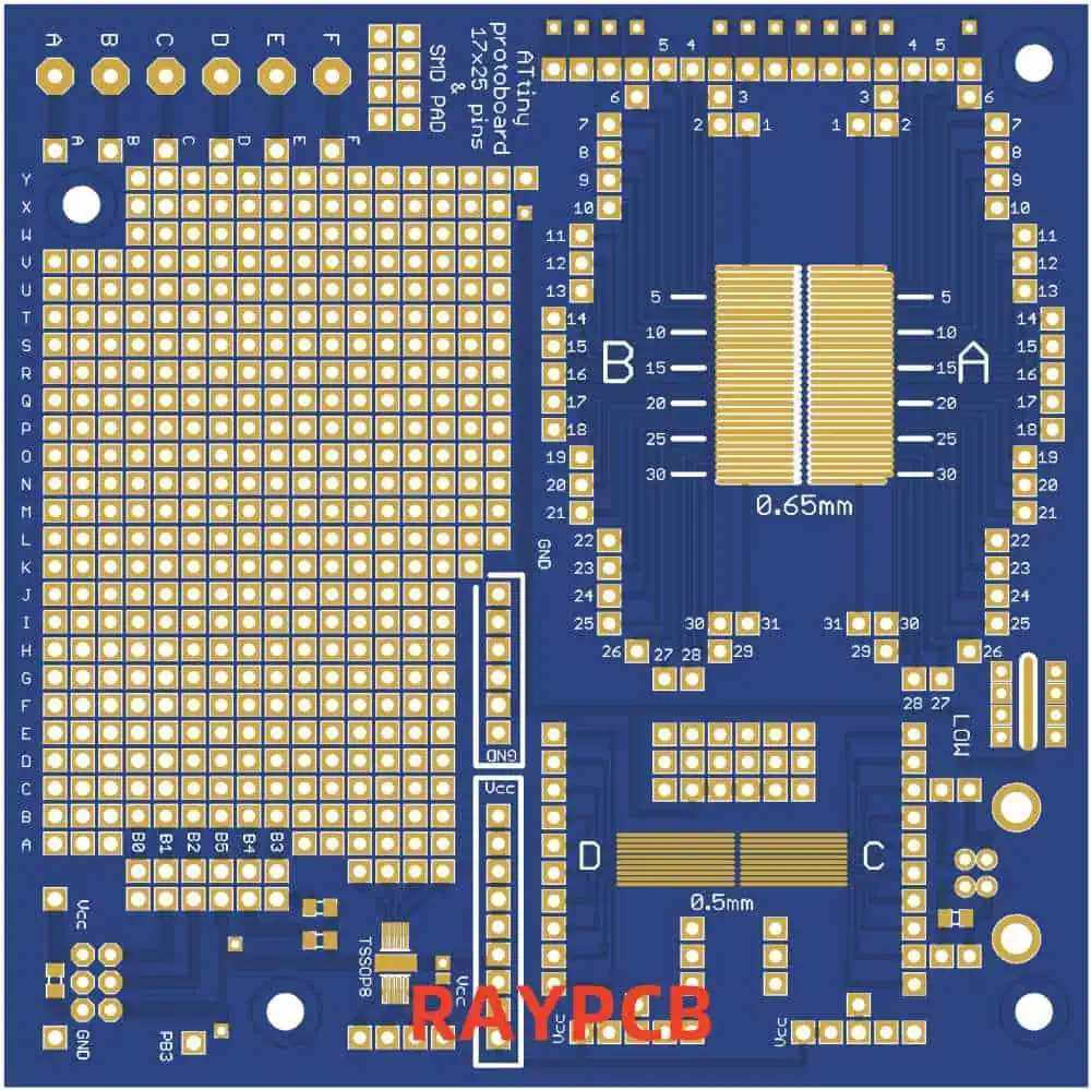
Accurately counting the total number of Surface Mount Device (SMD) pads in a PCB design is crucial for manufacturing planning, cost estimation, and quality control. This comprehensive guide explores various methods, tools, and best practices for determining the exact number of SMD pads in your design.

Understanding SMD Pad Types
Common SMD Pad Categories
| Pad Type | Description | Common Usage |
| Rectangular | Basic rectangular shape | General components |
| Round | Circular shape | Pin 1 indicators, vias |
| Custom | Special shapes | RF, thermal applications |
| Oblong | Elongated pads | Mechanical stability |
| Thermal | With thermal relief | Power components |
Standard Package Footprints
| Package Type | Number of Pads | Common Applications |
| SOT-23 | 3-6 | Small transistors |
| SOIC-8 | 8 | ICs, op-amps |
| QFP | 32-256 | Microcontrollers |
| BGA | 4-1000+ | Complex processors |
| 0402/0603/0805 | 2 | Passive components |
Manual Counting Methods
Component-Based Counting
Process Steps
- Create component categories
- Count components per category
- Multiply by pad count
- Sum all categories
Component Grouping Example
| Component Type | Pad Count | Quantity |
| 0402 Resistors | 2 | 100 |
| SOIC-8 | 8 | 10 |
| QFP-44 | 44 | 2 |
| LEDs | 2 | 20 |
Layer-Based Counting
Layer Analysis Process
| Layer | What to Count | Considerations |
| Top Layer | All SMD pads | Exclude through-holes |
| Bottom Layer | All SMD pads | Exclude through-holes |
| Inner Layers | N/A | SMD pads only on outer layers |
Automated Counting Methods
CAD Software Tools
Common Software Features
| Feature | Description | Accuracy |
| Pad Counter | Direct pad counting | Very High |
| BOM Analysis | Component-based counting | High |
| Layer Statistics | Layer-based counting | High |
| Design Rules | Pad verification | Medium |
Software-Specific Methods
| Software | Tool Location | Features |
| Altium | Reports → Board Statistics | Complete pad analysis |
| KiCad | PCB Editor → Statistics | Basic pad counting |
| Eagle | ULP Scripts | Customizable counting |
| OrCAD | Reports → Statistics | Detailed analysis |
Verification Methods
Cross-Checking Techniques
| Method | Reliability | Time Required |
| Visual Inspection | Medium | High |
| BOM Verification | High | Medium |
| Layer Comparison | High | Low |
| Script Validation | Very High | Low |
Common Error Sources
| Error Type | Cause | Prevention |
| Missing Pads | Hidden layers | Layer visibility check |
| Double Counting | Overlapping components | Component placement check |
| Wrong Classification | Incorrect pad types | Design rule check |
| Script Errors | Software bugs | Multiple verification methods |
Documentation and Reporting
Report Components
Essential Information
| Information Type | Purpose | Format |
| Total Pad Count | Manufacturing planning | Numeric |
| Pad Distribution | Layer balance | Percentage |
| Component Summary | BOM verification | Table |
| Special Pad Types | Process planning | List |
Report Format Example
| Category | Top Layer | Bottom Layer |
| SMD Pads | 450 | 320 |
| Thermal Pads | 12 | 8 |
| Custom Pads | 4 | 2 |
| Total | 466 | 330 |
Manufacturing Considerations
Pad Count Impact
Process Planning
| Aspect | Impact | Consideration |
| Stencil Design | Direct | Aperture count |
| Assembly Time | Direct | Pick-and-place programming |
| Inspection Points | Direct | AOI programming |
| Defect Rate | Indirect | Quality control planning |
Cost Implications
| Factor | Relationship | Cost Impact |
| Stencil Cost | Linear | Medium |
| Assembly Time | Linear | High |
| Testing Time | Linear | Medium |
| Rework Risk | Exponential | High |
Quality Control
Inspection Methods
| Method | Coverage | Time Required |
| Visual | 100% | High |
| AOI | 100% | Low |
| X-Ray | Selective | Medium |
| Flying Probe | 100% | High |
Defect Analysis
| Defect Type | Related to Pad Count | Prevention Method |
| Solder Bridges | Yes | Proper spacing |
| Missing Solder | Yes | Stencil design |
| Misalignment | Yes | Fiducial placement |
| Component Damage | No | Proper handling |
Frequently Asked Questions
Q1: Why is accurate pad counting important?
A: Accurate pad counting is crucial for:
- Manufacturing cost estimation
- Assembly time planning
- Quality control processes
- Material requirements calculation
- Testing procedure development Inaccurate counts can lead to production delays and cost overruns.
Q2: What’s the most reliable method for counting SMD pads?
A: The most reliable method is a combination of:
- Automated CAD software counting
- BOM-based verification
- Cross-checking between different methods
- Manual verification of special cases This multi-layered approach helps ensure accuracy.
Q3: How do I handle special pad types in the count?
A: Special pad types should be:
- Clearly identified in the design
- Counted separately from standard pads
- Documented in the BOM
- Verified with manufacturing team
- Included in final count with appropriate notes Special attention to thermal pads and custom shapes is essential.
Q4: What are common sources of pad counting errors?
A: Common errors include:
- Overlooking components on bottom layer
- Double-counting dual-side components
- Missing thermal or special pads
- Incorrect component footprint definitions
- Software calculation errors Regular verification and cross-checking helps prevent these errors.
Q5: How can I optimize my design for pad count verification?
A: Optimization strategies include:
- Using consistent component libraries
- Maintaining organized layer structure
- Implementing clear naming conventions
- Regular design rule checks
- Documenting special cases Good organization from the start makes verification easier.
Conclusion
Finding the total number of SMD pads in a PCB design requires a systematic approach combining automated tools, manual verification, and proper documentation. Success depends on understanding different pad types, using appropriate counting methods, and implementing proper verification procedures. By following the guidelines in this document and maintaining good documentation practices, you can ensure accurate pad counts for your PCB designs.