A Proposed Mechanism and Remedy for Ball-in-Socket and Foot-in-Mud Soldering Defects on Ball Grid Array and Quad Flat Pack Components

Soldering Balls

Do you involve in electronic PCB board production has probably encountered the phenomenon of “head-in-pillow” defects when soldering BGAs. Here is an interesting technical article describing this type of defect and an effective method to prevent it. 

Powered By EmbedPress

A Proposed Mechanism and Remedy for Ball-in-Socket and Foot-in-Mud Soldering Defects on Ball Grid Array and Quad Flat Pack Components

The miniaturization of electronic components has driven the widespread adoption of advanced packaging technologies such as Ball Grid Array (BGA) and Quad Flat Pack (QFP) components. While these packages offer superior electrical performance and higher pin density, they also introduce unique soldering challenges that can compromise assembly reliability. Among the most concerning defects are the “ball-in-socket” phenomenon affecting BGA components and the “foot-in-mud” defect commonly observed in QFP assemblies. Understanding the underlying mechanisms behind these defects and implementing effective remediation strategies is crucial for maintaining high-quality electronic assemblies.

Understanding Ball-in-Socket Defects in BGA Components

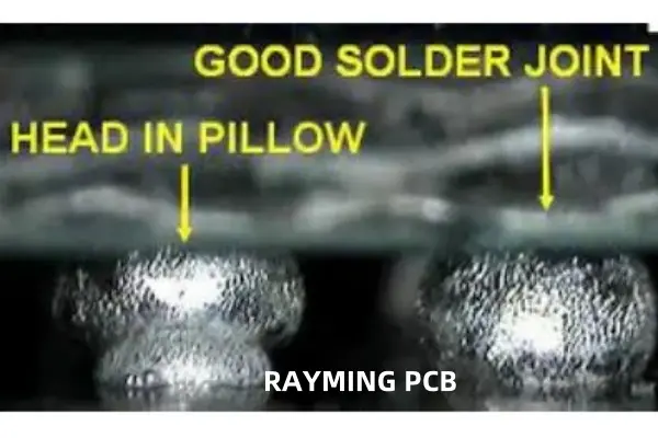
The ball-in-socket defect represents one of the most subtle yet problematic soldering issues in BGA assembly. This defect occurs when the solder ball from the BGA component fails to fully coalesce with the solder paste deposited on the PCB pad, resulting in a hollow cavity or “socket” formation around the solder ball. From external inspection, these joints may appear acceptable, making this defect particularly insidious as it often escapes visual detection while significantly compromising joint reliability.

The formation mechanism of ball-in-socket defects involves several interconnected factors. During the reflow process, the solder paste on the PCB pad begins to melt and wet the surface. Simultaneously, the solder ball attached to the BGA component also reaches its melting point. Under ideal conditions, these two molten solder masses should merge completely, forming a homogeneous joint upon cooling. However, when process parameters are suboptimal, incomplete coalescence occurs.

The primary contributing factors include insufficient reflow temperature profiles that fail to achieve complete solder melting, inadequate dwell time at peak temperature preventing full metallurgical bonding, contamination or oxidation on either the solder ball or PCB pad surface that inhibits proper wetting, and mismatched solder alloy compositions between the ball and paste that create different melting characteristics.

Additionally, the presence of flux residues or volatile compounds that fail to escape during reflow can create gas pockets that prevent complete solder fusion. The surface tension forces between the partially molten solder masses can also contribute to maintaining separation rather than promoting coalescence.

Foot-in-Mud Defects in QFP Components

The foot-in-mud defect affects QFP components and manifests as excessive solder buildup around the component leads, creating an appearance reminiscent of feet stuck in thick mud. This defect is characterized by irregular solder joint geometry with excessive fillet formation that can bridge adjacent pins or create stress concentrations that compromise long-term reliability.

The mechanism behind foot-in-mud formation typically involves excessive solder paste deposition combined with poor solder flow characteristics during reflow. When too much solder paste is applied to the PCB pads, the excess material must flow somewhere during the melting process. In QFP assemblies, this excess solder tends to accumulate around the component leads, particularly in the heel and toe regions of the joint.

Several factors contribute to this defect, including over-application of solder paste due to incorrect stencil design or printing parameters, inadequate component placement force that fails to displace excess paste, improper reflow profile that promotes solder spreading rather than controlled wetting, and flux formulations that provide insufficient surface tension control during the molten phase.

The component’s gull-wing lead design, while beneficial for visual inspection and rework, can exacerbate foot-in-mud formation by creating natural collection points for excess solder. The capillary action between the lead and PCB surface can draw additional molten solder into the joint area, further contributing to the defect formation.

Proposed Remediation Strategies

Addressing these soldering defects requires a comprehensive approach that encompasses process optimization, material selection, and quality control measures. For ball-in-socket defects in BGA assemblies, the primary focus should be on reflow profile optimization. The temperature profile must ensure complete melting of both the solder balls and paste while providing sufficient time above liquidus temperature for complete coalescence.

Implementing a gradual ramp rate during the preheat phase helps minimize thermal shock while ensuring uniform temperature distribution across the assembly. The peak temperature should exceed the solder alloy liquidus point by an appropriate margin, typically 20-30ยฐC for SAC alloys, while maintaining this temperature for 60-90 seconds to ensure complete metallurgical bonding.

Surface preparation plays a crucial role in preventing ball-in-socket formation. Both the BGA component and PCB pads must be free from oxidation, contamination, and flux residues that could inhibit proper wetting. Implementing controlled atmosphere reflow using nitrogen can significantly reduce oxidation and improve solder flow characteristics.

For foot-in-mud defects in QFP assemblies, stencil design optimization is paramount. The aperture size and shape must be carefully calculated to deposit the correct volume of solder paste for each pad size. Implementing area ratio calculations and considering the paste release characteristics can help achieve optimal paste deposition. Typically, maintaining an area ratio between 0.6 and 1.5 provides good paste release while preventing over-deposition.

Component placement parameters also require attention. The placement force should be sufficient to displace excess paste without damaging the component or creating placement accuracy issues. Implementing force feedback during placement can help ensure consistent results across different component types and sizes.

Process Control and Quality Assurance

Effective prevention of these soldering defects requires robust process control and monitoring systems. Statistical process control should be implemented for critical parameters including paste printing thickness and registration, component placement accuracy and force, and reflow temperature profile consistency across the conveyor width.

Advanced inspection techniques such as X-ray imaging can detect ball-in-socket defects that escape visual inspection. Automated X-ray systems can be programmed to identify the characteristic void patterns associated with incomplete solder coalescence, enabling early detection and process correction.

For foot-in-mud defects, automated optical inspection systems can be configured to detect excessive solder buildup and joint geometry irregularities. Implementing measurement algorithms that assess fillet height and width can provide quantitative feedback for process optimization.

Conclusion

Ball-in-socket and foot-in-mud soldering defects represent significant challenges in modern electronic assembly, requiring careful attention to process parameters, material properties, and quality control measures. By understanding the underlying formation mechanisms and implementing comprehensive remediation strategies, manufacturers can achieve reliable, high-quality solder joints that meet the demanding requirements of today’s electronic products. Continuous monitoring and process optimization remain essential for maintaining consistent assembly quality and preventing these subtle but critical defects from compromising product reliability.

RO3000 Series Bondply Data Sheet Processing Guidelines

Rogers TMM 10i Laminate

The Rogers RO3000 Series Bondply Data Sheet provides essential guidelines for processing high-frequency circuit materials. It emphasizes precise handling, optimal lamination, and controlled drilling to maintain dielectric properties. Proper cleaning, temperature control, and pressure settings are crucial for successful bonding. Adhering to these guidelines ensures consistent performance, reliability, and signal integrity in high-frequency applications like RF and microwave circuits.

Powered By EmbedPress

Complete Guide to BOM Electronic Components Purchase

HOW TO MAKE BOM

Introduction

A Bill of Materials (BOM) is a comprehensive list of components, materials, and assemblies required to manufacture a product. In the context of electronics, the BOM is a critical document that outlines all the electronic components needed to build a Printed Circuit Board (PCB) or an electronic device. Purchasing electronic components for a BOM can be a complex process, involving careful planning, supplier selection, and quality assurance. This guide provides a complete overview of the BOM electronic components purchase process, from understanding the BOM to sourcing components and managing inventory.


1. Understanding the BOM

1.1 What is a BOM?

A BOM is a detailed list of all the parts and materials required to manufacture a product. In electronics, the BOM includes:

1.2 Types of BOM

There are several types of BOM, each serving a different purpose:

  • Engineering BOM (EBOM):ย Focuses on the design and engineering aspects of the product.

  • Manufacturing BOM (MBOM):ย Includes all the components and materials needed for production.

  • Service BOM (SBOM):ย Lists the parts required for maintenance and repair.

1.3 Importance of an Accurate BOM

An accurate BOM is essential for:

  • Cost Estimation:ย Helps in calculating the total cost of materials.

  • Procurement Planning:ย Ensures that all components are available when needed.

  • Production Efficiency:ย Reduces the risk of delays and errors during manufacturing.

  • Inventory Management:ย Helps in maintaining optimal stock levels.


2. Preparing for Component Purchase

2.1 Reviewing the BOM

Before purchasing components, review the BOM to ensure it is complete and accurate. Check for:

  • Component Specifications:ย Ensure that all components meet the required specifications (e.g., resistance, capacitance, voltage rating).

  • Quantities:ย Verify the quantities needed for each component.

  • Alternate Parts:ย Identify any alternate or substitute components that can be used if the primary part is unavailable.

2.2 Identifying Critical Components

Some components are more critical than others due to their function, availability, or cost. Identify these components early to prioritize their procurement.

2.3 Budgeting

Estimate the total cost of the components based on the BOM. Consider factors such as:

  • Component Costs:ย Unit prices of individual components.

  • Shipping Costs:ย Costs associated with transporting components.

  • Taxes and Duties:ย Import duties and taxes that may apply.


3. Sourcing Electronic Components

3.1 Choosing Suppliers

Selecting the right suppliers is crucial for ensuring the quality and availability of components. Consider the following factors when choosing suppliers:

  • Reputation:ย Look for suppliers with a good reputation for quality and reliability.

  • Lead Times:ย Ensure that the supplier can deliver components within the required timeframe.

  • Minimum Order Quantities (MOQs):ย Check if the supplier has MOQs that align with your needs.

  • Certifications:ย Verify that the supplier has relevant certifications (e.g., ISO 9001).

3.2 Types of Suppliers

There are several types of suppliers to consider:

  • Manufacturers:ย Directly produce the components.

  • Distributors:ย Authorized resellers of components from manufacturers.

  • Brokers:ย Intermediaries who source components from various suppliers.

  • Online Marketplaces:ย Platforms like Digi-Key, Mouser, and Arrow that offer a wide range of components.

3.3 Requesting Quotes

Request quotes from multiple suppliers to compare prices and terms. Provide the following information in your request:

  • Component Part Numbers:ย Ensure that the part numbers match the BOM.

  • Quantities:ย Specify the quantities needed for each component.

  • Delivery Requirements:ย Indicate the required delivery date and location.

3.4 Evaluating Quotes

When evaluating quotes, consider:

  • Price:ย Compare the total cost, including shipping and taxes.

  • Lead Time:ย Ensure that the supplier can meet your delivery requirements.

  • Terms and Conditions:ย Review payment terms, return policies, and warranties.


4. Placing Ordersbom bill of material

4.1 Order Confirmation

Once you have selected a supplier, confirm the order by providing:

  • Purchase Order (PO):ย A formal document outlining the order details.

  • Shipping Information:ย Delivery address and contact information.

  • Payment Details:ย Payment method and terms.

4.2 Tracking Orders

Track the status of your orders to ensure timely delivery. Most suppliers provide tracking information that allows you to monitor the progress of your shipment.

4.3 Receiving and Inspecting Components

Upon receiving the components, inspect them to ensure they meet the required specifications. Check for:

  • Correct Part Numbers:ย Verify that the received components match the part numbers in the BOM.

  • Quantity:ย Ensure that the correct quantity has been delivered.

  • Quality:ย Inspect for any physical damage or defects.


5. Managing Inventory

5.1 Inventory Tracking

Maintain an inventory tracking system to monitor stock levels and usage. This can be done using:

  • Spreadsheets:ย Simple and cost-effective for small-scale operations.

  • Inventory Management Software:ย More advanced solutions that offer real-time tracking and reporting.

5.2 Reordering Components

Set up a reordering system to ensure that you never run out of critical components. Consider:

  • Reorder Points:ย The stock level at which you need to place a new order.

  • Safety Stock:ย A buffer stock to account for variability in demand and lead times.

5.3 Managing Obsolete Components

Electronic components can become obsolete due to technological advancements or changes in market demand. To manage obsolete components:

  • Identify Obsolete Parts:ย Regularly review your BOM for components that are no longer available.

  • Source Alternatives:ย Find alternate parts or redesign the circuit to use available components.

  • Stockpile Critical Parts:ย If possible, stockpile critical components that are at risk of becoming obsolete.


6. Quality Assurance

6.1 Component Testing

Test components to ensure they meet the required specifications. Common tests include:

  • Electrical Testing:ย Verify electrical properties such as resistance, capacitance, and voltage rating.

  • Functional Testing:ย Test the component in a real-world application to ensure it performs as expected.

6.2 Supplier Audits

Conduct regular audits of your suppliers to ensure they maintain high-quality standards. Audits can include:

  • Factory Visits:ย Inspect the supplier’s manufacturing facilities.

  • Quality Certifications:ย Verify that the supplier holds relevant quality certifications.

  • Performance Reviews:ย Assess the supplier’s performance based on delivery times, defect rates, and customer service.

6.3 Handling Defective Components

If you receive defective components, follow these steps:

  • Document the Issue:ย Record details of the defect, including part numbers, quantities, and photos.

  • Contact the Supplier:ย Notify the supplier and request a replacement or refund.

  • Update Inventory:ย Remove defective components from your inventory to prevent them from being used in production.


7. Cost Management

7.1 Negotiating Prices

Negotiate with suppliers to get the best possible prices. Consider:

  • Volume Discounts:ย Request discounts for large orders.

  • Long-Term Contracts:ย Commit to long-term contracts in exchange for lower prices.

  • Bundling:ย Combine multiple orders to reduce shipping costs.

7.2 Reducing Costs

Implement strategies to reduce the overall cost of components:

  • Design for Manufacturability (DFM):ย Optimize the design to use standard, readily available components.

  • Value Engineering:ย Identify and eliminate unnecessary costs without compromising quality.

  • Bulk Purchasing:ย Purchase components in bulk to take advantage of volume discounts.


Conclusion

Purchasing electronic components for a BOM is a critical process that requires careful planning, supplier selection, and quality assurance. By understanding the BOM, sourcing components from reliable suppliers, and managing inventory effectively, you can ensure the successful production of your electronic devices. Additionally, implementing cost management strategies and maintaining high-quality standards will help you achieve a competitive edge in the market. Whether you are a hobbyist or a professional, this guide provides the essential knowledge and tools to navigate the complex world of BOM electronic components purchase.

Comparison Between Organic Core and Glass Core Substrates

In the realm of electronics and semiconductor manufacturing, the choice of substrate material plays a pivotal role in determining the performance, reliability, and cost-effectiveness of the final product. Two prominent types of substrates used in various applications are organic core substrates and glass core substrates. Each type has its unique set of properties, advantages, and limitations, making them suitable for different applications. This article delves into a comprehensive comparison between organic core and glass core substrates based on the provided data, covering aspects such as core thickness, via drill size, thermal conductivity, dielectric constant, material composition, cost, applications, electrical properties, thickness uniformity, mechanical strength, and raw material suppliers.

YouTube video

Core Thickness

Organic Core Substrate:

  • Range: ~30ฮผm to 200ฮผm
  • Characteristics: Organic core substrates typically have a thinner core compared to glass core substrates. This thinness allows for greater flexibility and lighter weight, which is advantageous in applications where space and weight are critical factors.

Glass Core Substrate:

  • Range: ~200ฮผm to 1100ฮผm
  • Characteristics: Glass core substrates are generally thicker, providing better mechanical stability and rigidity. This makes them suitable for applications requiring high precision and durability, such as in IC packaging and high-frequency RF applications.

Via Drill Size

Organic Core Substrate:

  • Minimum Size: ~50ฮผm
  • Via Type: TSV (Through-Silicon Via), Mechanical Drill
  • Characteristics: The larger via drill size in organic core substrates facilitates easier manufacturing processes and is cost-effective. However, it may limit the density of interconnections, which can be a drawback in high-density applications.

Glass Core Substrate:

  • Minimum Size: ~5ฮผm to 15ฮผm
  • Via Type: TGV (Through-Glass Via), Laser Drilled
  • Characteristics: The significantly smaller via drill size in glass core substrates allows for higher interconnection density, which is crucial for advanced packaging and high-frequency applications. The precision of laser drilling also ensures high-quality vias with minimal defects.

Thermal Conductivity

Organic Core Substrate:

  • Range: ~0.8-1.4 W/m-K (Low)
  • Characteristics: Organic materials generally have lower thermal conductivity, which can lead to heat buildup in high-power applications. This necessitates additional thermal management solutions, such as heat sinks or thermal vias.

Glass Core Substrate:

  • Range: ~0.2-0.5 W/m-K (High)
  • Characteristics: Glass core substrates exhibit higher thermal conductivity, making them more efficient at dissipating heat. This property is particularly beneficial in high-power and high-frequency applications where thermal management is critical.

Dielectric Constant

Organic Core Substrate:

  • Value: ~3
  • Characteristics: The dielectric constant of organic core substrates is relatively low, which is advantageous for high-speed signal transmission. Lower dielectric constants reduce signal loss and improve the overall performance of high-frequency circuits.

Glass Core Substrate:

  • Value: ~2.5-3
  • Characteristics: Glass core substrates also have a low dielectric constant, comparable to organic core substrates. This makes them suitable for high-frequency applications where signal integrity is paramount.

Material Composition

Organic Core Substrate:

  • Materials: BT (Bismaleimide Triazine), epoxy resin, FR4
  • Characteristics: Organic core substrates are composed of polymer-based materials, which are lightweight and flexible. These materials are cost-effective and widely available, making them a popular choice for traditional PCBs.

Glass Core Substrate:

  • Materials: Borosilicate (SiO2)
  • Characteristics: Glass core substrates are made from borosilicate glass, which offers excellent mechanical and thermal properties. However, the material is more expensive and less flexible compared to organic materials.

Cost

Organic Core Substrate:

  • Cost: Low
  • Characteristics: The use of polymer-based materials and simpler manufacturing processes contribute to the lower cost of organic core substrates. This makes them an economical choice for a wide range of applications, especially in consumer electronics.

Glass Core Substrate:

  • Cost: High
  • Characteristics: The higher cost of glass core substrates is attributed to the expensive raw materials and the complex manufacturing processes involved, such as laser drilling for vias. This makes them more suitable for high-end applications where performance is critical.

Applications

Organic Core Substrate:

  • Applications: Traditional PCBs
  • Characteristics: Organic core substrates are widely used in traditional printed circuit boards (PCBs) due to their cost-effectiveness and flexibility. They are suitable for a broad range of consumer electronics, including smartphones, laptops, and home appliances.

Glass Core Substrate:

  • Applications: IC Packaging, High-Frequency RF Applications
  • Characteristics: Glass core substrates are preferred in advanced packaging and high-frequency RF applications due to their superior thermal and electrical properties. They are commonly used in high-performance computing, telecommunications, and aerospace industries.

Electrical Properties

Organic Core Substrate:

  • Properties: Excellent insulator
  • Characteristics: Organic core substrates provide excellent electrical insulation, which is crucial for preventing short circuits and ensuring reliable performance in electronic devices.

Glass Core Substrate:

  • Properties: Good insulator
  • Characteristics: While glass core substrates also offer good electrical insulation, their primary advantage lies in their thermal and mechanical properties, which are more critical in high-performance applications.

Thickness Uniformity

Organic Core Substrate:

  • Uniformity: Variation depending on the polymer type
  • Characteristics: The thickness uniformity of organic core substrates can vary based on the type of polymer used. This variability can affect the consistency of the substrate’s performance, especially in high-precision applications.

Glass Core Substrate:

  • Uniformity: High precision
  • Characteristics: Glass core substrates exhibit high precision in thickness uniformity, which is essential for applications requiring consistent performance and reliability, such as in IC packaging.

Mechanical Strength

Organic Core Substrate:

  • Strength: Flexible
  • Characteristics: The flexibility of organic core substrates makes them suitable for applications where the substrate may be subjected to bending or flexing, such as in flexible electronics.

Glass Core Substrate:

  • Strength: Fragile
  • Characteristics: Glass core substrates are more rigid and fragile compared to organic core substrates. While this fragility can be a limitation in some applications, it provides the necessary mechanical stability for high-precision applications.

Raw Material Suppliers

Organic Core Substrate:

  • Suppliers: ISOLA, Kyocera
  • Characteristics: The raw materials for organic core substrates are supplied by a wide range of global players, ensuring a steady supply chain and competitive pricing.

Glass Core Substrate:

  • Suppliers: COVIA, US SILICA, EVONIK
  • Characteristics: The raw materials for glass core substrates are supplied by a limited number of specialized manufacturers, which can impact the availability and cost of these substrates.

Substrate Manufacturers

Organic Core Substrate:

  • Manufacturers: TTM, Unimicron (Many global players)
  • Characteristics: The manufacturing of organic core substrates is carried out by numerous global players, leading to a competitive market and a wide range of options for consumers.

Glass Core Substrate:

  • Manufacturers: CORNING, AGC, NsG Group (Few only)
  • Characteristics: The manufacturing of glass core substrates is dominated by a few specialized companies, which can limit the availability and increase the cost of these substrates.

Conclusion

In summary, the choice between organic core and glass core substrates depends on the specific requirements of the application. Organic core substrates offer cost-effectiveness, flexibility, and excellent electrical insulation, making them suitable for traditional PCBs and consumer electronics. On the other hand, glass core substrates provide superior thermal conductivity, high precision, and mechanical stability, making them ideal for advanced packaging and high-frequency RF applications. Understanding the distinct properties and advantages of each substrate type is crucial for selecting the appropriate material to meet the performance and reliability needs of the intended application.

How to Apply UV Solder Mask to Your PCB Board at Home: A Step-by-Step Guide

Introduction

Applying a solder mask to a Printed Circuit Board (PCB) is a crucial step in the PCB manufacturing process. The solder mask protects the copper traces from oxidation, prevents solder bridges, and enhances the overall durability of the board. While professional PCB manufacturers use advanced equipment to apply solder masks, it is possible to apply a UV solder mask at home with the right tools and techniques. This guide provides a comprehensive, step-by-step process for applying UV solder mask to your PCB board at home.

YouTube video

1. Understanding UV Solder Mask

1.1 What is UV Solder Mask?

UV solder mask is a type of solder resist that cures (hardens) when exposed to ultraviolet (UV) light. It is typically supplied as a liquid or film and is applied to the PCB to cover the copper traces, leaving only the pads exposed for soldering.

1.2 Benefits of UV Solder Mask

  • Protection:ย Protects copper traces from oxidation and environmental damage.
  • Insulation:ย Prevents electrical shorts by insulating conductive traces.
  • Solder Control:ย Prevents solder from bridging between closely spaced pads.
  • Aesthetic Appeal:ย Provides a professional finish to the PCB.

1.3 Tools and Materials Required

To apply UV solder mask at home, you will need the following tools and materials:

  1. UV Solder Mask Liquid or Film:ย Available in various colors (green, blue, red, etc.).
  2. UV Light Source:ย A UV lamp or UV curing chamber.
  3. Squeegee or Brush:ย For spreading the solder mask evenly.
  4. Photo Film or Transparency Sheet:ย For creating a solder mask stencil.
  5. PCB Cleaning Supplies:ย Isopropyl alcohol, lint-free cloth, and a brush.
  6. Plastic Container:ย For mixing and storing the solder mask.
  7. Protective Gear:ย Gloves, safety glasses, and a mask to protect against fumes.

2. Step-by-Step Guide to Applying UV Solder Mask

2.1 Step 1: Prepare the PCB

2.1.1 Clean the PCB

Before applying the solder mask, ensure that the PCB is clean and free of dust, grease, and oxidation. Follow these steps:

  1. Wipe the PCB with a lint-free cloth soaked in isopropyl alcohol.
  2. Use a soft brush to remove any debris from the traces and pads.
  3. Allow the PCB to dry completely.

2.1.2 Inspect the PCB

Inspect the PCB for any defects, such as scratches or exposed copper. Repair any issues before proceeding.

2.2 Step 2: Create the Solder Mask Stencil

2.2.1 Design the Stencil

Using PCB design software (e.g., KiCad, Eagle, or Altium), create a solder mask layer that exposes only the pads and vias. Export this layer as a high-resolution image or PDF.

2.2.2 Print the Stencil

Print the solder mask layer onto a photo film or transparency sheet using a laser printer. Ensure that the print is dark and opaque to block UV light effectively.

2.3 Step 3: Apply the UV Solder Mask

2.3.1 Mix the Solder Mask (if required)

If using a two-part UV solder mask, mix the components according to the manufacturer’s instructions. Stir gently to avoid introducing air bubbles.

2.3.2 Apply the Solder Mask

There are two main methods for applying UV solder mask: liquid application and film application.

Liquid Application Method:
  1. Pour a small amount of UV solder mask liquid onto the PCB.
  2. Use a squeegee or brush to spread the liquid evenly over the entire surface.
  3. Ensure that the solder mask covers all the traces while leaving the pads exposed.
Film Application Method:
  1. Cut a piece of UV solder mask film slightly larger than the PCB.
  2. Peel off the protective layer and carefully place the film onto the PCB.
  3. Use a roller or squeegee to remove air bubbles and ensure proper adhesion.

2.4 Step 4: Align and Expose the Stencil

2.4.1 Align the Stencil

Place the printed photo film or transparency sheet over the PCB, ensuring that the pads and vias align perfectly with the openings in the stencil.

2.4.2 Expose to UV Light

  1. Place the PCB and stencil under the UV light source.
  2. Expose the PCB to UV light for the recommended duration (usually 1-5 minutes, depending on the solder mask and UV light intensity).
  3. Rotate the PCB if necessary to ensure even exposure.

2.5 Step 5: Develop the Solder Mask

2.5.1 Remove the Stencil

After exposure, carefully remove the photo film or transparency sheet from the PCB.

2.5.2 Rinse the PCB

Rinse the PCB with water or a developer solution (as specified by the solder mask manufacturer) to remove the uncured solder mask. Use a soft brush to gently scrub the surface.

2.5.3 Dry the PCB

Allow the PCB to dry completely. You can use compressed air or a lint-free cloth to speed up the drying process.

2.6 Step 6: Cure the Solder Mask

2.6.1 Final UV Exposure

Place the PCB under the UV light source again for a final cure. This step ensures that the solder mask is fully hardened and durable.

2.6.2 Inspect the PCB

Inspect the PCB for any defects, such as incomplete coverage or misaligned pads. Touch up any areas if necessary.


3. Tips for Success

3.1 Work in a Clean Environment

Dust and debris can affect the quality of the solder mask application. Work in a clean, well-ventilated area to minimize contamination.

3.2 Use High-Quality Materials

Invest in high-quality UV solder mask and photo film to ensure the best results. Cheap materials may lead to poor adhesion or incomplete curing.

3.3 Practice on Scrap PCBs

If you are new to applying solder masks, practice on scrap PCBs before working on your final project. This will help you refine your technique and avoid mistakes.

3.4 Follow Manufacturer Instructions

Always follow the manufacturer’s instructions for mixing, applying, and curing the solder mask. Different products may have specific requirements.


4. Troubleshooting Common Issues

4.1 Incomplete Coverage

  • Cause:ย Insufficient solder mask application or uneven spreading.
  • Solution:ย Apply a thicker layer of solder mask and use a squeegee to spread it evenly.

4.2 Solder Mask Peeling

  • Cause:ย Poor adhesion due to contamination or improper curing.
  • Solution:ย Clean the PCB thoroughly before application and ensure proper UV exposure.

4.3 Misaligned Pads

  • Cause:ย Incorrect alignment of the stencil.
  • Solution:ย Double-check the alignment before exposing the PCB to UV light.

4.4 Air Bubbles

  • Cause:ย Trapped air during application.
  • Solution:ย Use a roller or squeegee to remove air bubbles before curing.

5. Advantages of Applying UV Solder Mask at Home

5.1 Cost-Effective

Applying solder mask at home can save money compared to outsourcing the process to a professional PCB manufacturer.

5.2 Customization

You have full control over the design and application process, allowing for greater customization.

5.3 Learning Experience

The process provides valuable hands-on experience and a deeper understanding of PCB manufacturing.


Conclusion

Applying UV solder mask to your PCB board at home is a rewarding and cost-effective way to enhance the durability and functionality of your PCBs. By following the step-by-step guide outlined above, you can achieve professional-quality results with the right tools and techniques. Whether you are a hobbyist or a professional, mastering this skill will enable you to create high-quality PCBs for a wide range of applications. With practice and attention to detail, you can confidently apply UV solder mask to your PCB projects at home.

RO3000 Laminate Data Sheet RO3003 โ€“ RO3006 โ€“ RO3010 โ€“ RO3035

RO3003 material

The RO3000 series laminates are high-frequency circuit materials designed for demanding RF and microwave applications. This family includes RO3003, RO3006, RO3010, and RO3035, each offering different dielectric constants ranging from 3.0 to 3.5. These materials provide excellent electrical and mechanical stability, low loss, and consistent dielectric constant across a wide frequency range, making them ideal for high-performance RF/microwave circuits.

Powered By EmbedPress

RO3003 โ€“ RO3006 โ€“ RO3010 โ€“ RO3035

The Rogers RO3000 series represents a family of high-performance ceramic-filled PTFE composite laminates specifically engineered for demanding RF and microwave applications. This comprehensive analysis examines the four primary variants in the series: RO3003, RO3006, RO3010, and RO3035, each offering distinct dielectric properties while maintaining consistent mechanical characteristics that make them ideal for commercial microwave and RF circuit designs.

YouTube video

Series Overview and Core Technology

The RO3000 series utilizes ceramic-filled polytetrafluoroethylene (PTFE) composite technology, which provides the foundation for exceptional electrical and mechanical stability across all frequency ranges. This family was specifically designed to deliver outstanding performance at competitive prices, making high-frequency circuit design more accessible for commercial applications. The ceramic filling in the PTFE matrix ensures dimensional stability while maintaining the excellent electrical properties that PTFE is known for.

What sets the RO3000 series apart from other high-frequency laminates is the consistent mechanical properties across all dielectric constant variants. This uniformity allows designers to develop complex multilayer board constructions using different dielectric constant materials for individual layers without encountering warpage or reliability issues that typically plague mixed-material designs.

Individual Material Specifications

RO3003 Laminates

RO3003 represents the lowest dielectric constant option in the series, featuring a dielectric constant (ฮตr) of 3.0 ยฑ 0.04. This material exhibits exceptionally low dielectric loss, with a dissipation factor (tan ฮด) of only 0.0013 at 10 GHz, making it suitable for applications extending up to 30-40 GHz. The low dielectric constant and minimal loss characteristics make RO3003 particularly valuable for millimeter-wave applications, precision stripline circuits, and high-performance antenna systems where signal integrity is paramount.

The material demonstrates excellent thermal stability with a coefficient of thermal expansion (CTE) in the X and Y directions of 17 ppm/ยฐC, which precisely matches that of copper. This matching ensures exceptional dimensional stability during thermal cycling, with typical etch shrinkage after etching and baking of less than 0.5 mils per inch. The Z-axis CTE of 24 ppm/ยฐC provides outstanding plated through-hole reliability even in severe thermal environments.

RO3006 Laminates

RO3006 features a dielectric constant of 6.15, positioning it as the mid-range option for applications requiring higher capacitance per unit area while maintaining low loss characteristics. Like its RO3003 counterpart, RO3006 exhibits a dissipation factor of 0.0013 at 10 GHz, ensuring minimal signal degradation across the frequency spectrum. The higher dielectric constant makes RO3006 particularly suitable for compact circuit designs where size reduction is critical without compromising electrical performance.

The thermal stability coefficient in the Z-direction reaches an impressive -3 ppm/ยฐC when measured over the temperature range from -50ยฐC to +150ยฐC at 10 GHz. This exceptional temperature stability eliminates the step-change phenomenon in dielectric constant that occurs in traditional PTFE glass materials near room temperature, ensuring consistent performance across varying environmental conditions.

RO3010 Laminates

RO3010 offers a dielectric constant of 10.2, representing the highest value in the series for applications requiring maximum miniaturization and high capacitance density. This material maintains the same excellent loss characteristics as other series members while providing the electrical properties needed for extremely compact antenna designs and high-density filter applications. The higher dielectric constant enables significant size reduction in circuit designs, particularly valuable in space-constrained applications such as automotive radar systems and portable communication devices.

The material maintains the same mechanical stability characteristics as other RO3000 series members, ensuring that the benefits of higher dielectric constant don’t come at the expense of mechanical reliability or processing difficulties.

RO3035 Laminates

RO3035 features a dielectric constant of 3.5, providing a middle ground between RO3003 and RO3006 for applications requiring specific impedance characteristics. This variant maintains the excellent electrical performance standards of the series while offering designers additional flexibility in circuit design optimization. The material demonstrates the same exceptional temperature stability as RO3003, making it suitable for applications where environmental conditions may vary significantly.

Mechanical and Thermal Properties

All RO3000 series materials share identical mechanical properties, which represents a significant advantage for multilayer circuit design. The coefficient of thermal expansion in the X and Y directions of 17 ppm/ยฐC matches copper exactly, ensuring that the substrate and conductor expand at the same rate during temperature changes. This matching prevents stress-related failures and maintains circuit integrity over extended temperature cycling.

The Z-axis CTE of 24 ppm/ยฐC provides exceptional reliability for plated through-hole connections, even under severe thermal stress conditions. This property is particularly important for applications in automotive, aerospace, and industrial environments where temperature extremes are common.

The dielectric constant versus temperature relationship for all RO3000 materials is remarkably stable, eliminating the performance variations that can plague other high-frequency materials. This stability ensures predictable circuit performance across the entire operating temperature range, reducing the need for temperature compensation in critical applications.

Processing and Manufacturing Considerations

RO3000 series laminates can be processed using standard PTFE circuit board fabrication techniques with minor modifications outlined in Rogers Corporation’s fabrication guidelines. The materials are compatible with conventional drilling, etching, and plating processes, though special handling procedures are required due to the PTFE content.

The ceramic filling in the PTFE matrix provides improved dimensional stability compared to unfilled PTFE materials while maintaining the excellent electrical properties. This enhancement allows for tighter tolerance control during manufacturing and improved yield rates in production environments.

Standard thickness tolerances are maintained across the series, with typical values of ยฑ0.0013 inches (ยฑ0.033 mm) for most standard thicknesses. The materials are available in various copper cladding weights, including 0.5 oz, 1 oz, and 2 oz configurations, providing flexibility for different application requirements.

Applications and Performance Advantages

The RO3000 series finds extensive application in automotive collision avoidance systems, GPS satellite antennas, cellular and pager telecommunications systems, patch antennas for wireless communications, direct broadcast satellites, cable system datalinks, remote meter reading systems, and power backplane applications. The consistent mechanical properties across dielectric constants make the series particularly valuable for complex multilayer designs that require different electrical characteristics in different layers.

The series offers significant cost advantages compared to traditional PTFE-based microwave laminates while maintaining comparable electrical performance. This cost-effectiveness makes high-frequency design more accessible for commercial applications where budget constraints are significant factors.

The low dielectric loss characteristics enable the materials to be used effectively in applications up to 30-40 GHz, covering most commercial RF and microwave frequency bands. The stable dielectric constant across temperature and frequency ranges ensures predictable performance in varying environmental conditions.

Conclusion

The RO3000 series represents a mature and well-optimized family of high-frequency circuit materials that successfully balance performance, reliability, and cost-effectiveness. The four variants โ€“ RO3003, RO3006, RO3010, and RO3035 โ€“ provide designers with a comprehensive range of dielectric constants while maintaining consistent mechanical properties that simplify multilayer design challenges.

The exceptional thermal stability, low loss characteristics, and processing compatibility make the RO3000 series an excellent choice for demanding RF and microwave applications. The materials’ proven track record in commercial applications, combined with their competitive pricing, positions them as industry standards for high-frequency circuit design where reliability and performance are essential requirements.

What is solder mask dam?

Introduction

In the world of Printed Circuit Board (PCB) manufacturing, the solder mask plays a crucial role in ensuring the reliability and functionality of the final product. Among the various features of a solder mask, the solder mask dam is a critical element that often goes unnoticed but is essential for preventing solder-related defects. This article provides a comprehensive overview of what a solder mask dam is, its purpose, design considerations, and its importance in PCB manufacturing.

YouTube video

1. Understanding Solder Mask

Before diving into the specifics of a solder mask dam, it is essential to understand the solder mask itself.

1.1 What is Solder Mask?

Solder mask, also known as solder resist, is a thin, protective layer applied to the copper traces of a PCB. It is typically made of a polymer material that is resistant to heat, chemicals, and environmental factors. The primary functions of the solder mask include:

  • Protection:ย It protects the copper traces from oxidation, corrosion, and environmental damage.
  • Insulation:ย It prevents electrical shorts by insulating the conductive traces.
  • Solder Control:ย It prevents solder from bridging between closely spaced pads during the soldering process.

1.2 Types of Solder Mask

Solder masks come in various types, including:

  • Liquid Photoimageable Solder Mask (LPSM):ย Applied as a liquid and cured using UV light.
  • Dry Film Solder Mask:ย Applied as a dry film and laminated onto the PCB.
  • Epoxy-Based Solder Mask:ย Typically used for simpler designs and less demanding applications.

2. What is a Solder Mask Dam?

2.1 Definition

solder mask dam is a small, raised barrier of solder mask material that is intentionally left between two adjacent pads or features on a PCB. Its primary purpose is to prevent solder from flowing between these pads during the soldering process, thereby avoiding solder bridging and short circuits.

2.2 Purpose of a Solder Mask Dam

The solder mask dam serves several critical functions:

  1. Preventing Solder Bridging:ย By creating a physical barrier between adjacent pads, the solder mask dam prevents molten solder from forming unintended connections (bridges) during reflow soldering or wave soldering.
  2. Improving Solder Joint Quality:ย It ensures that solder is confined to the intended pads, resulting in better solder joint formation and reliability.
  3. Enhancing Electrical Isolation:ย The dam provides additional insulation between conductive traces, reducing the risk of electrical shorts.
  4. Facilitating Fine-Pitch Components:ย For components with fine-pitch leads (e.g., BGAs, QFPs), solder mask dams are essential for maintaining proper spacing and preventing defects.

3. Design and Implementation of Solder Mask Dams

3.1 Design Considerations

Designing an effective solder mask dam requires careful consideration of several factors:

3.1.1 Width and Height

  • The width of the solder mask dam must be sufficient to prevent solder from bridging but not so wide that it encroaches on the pad area.
  • The height of the dam is determined by the thickness of the solder mask layer, which is typically between 0.5 mils (0.013 mm) and 2 mils (0.05 mm).

3.1.2 Clearance

  • Adequate clearance must be maintained between the solder mask dam and the pad edges to ensure proper solder wetting and joint formation.
  • The clearance is often defined by the PCB manufacturer’s design rules and depends on the soldering process used.

3.1.3 Material Properties

  • The solder mask material must have good thermal and chemical resistance to withstand the soldering process without degrading.
  • It should also adhere well to the PCB substrate to prevent delamination.

3.2 Implementation Process

The implementation of solder mask dams involves the following steps:

  1. Design Phase:
    • The solder mask dam is defined in the PCB design files (e.g., Gerber files) as part of the solder mask layer.
    • The design software automatically generates the dam based on the specified clearance rules.
  2. Application Phase:
    • The solder mask is applied to the PCB using methods such as screen printing, curtain coating, or spray coating.
    • The areas where the dam is required are masked off during the application process.
  3. Curing Phase:
    • The solder mask is cured using UV light or heat to harden the material and ensure proper adhesion.
  4. Inspection Phase:
    • The solder mask dam is inspected for defects such as insufficient height, uneven coverage, or misalignment.

4. Importance of Solder Mask Dams in PCB Manufacturing

4.1 Preventing Solder Bridging

Solder bridging is one of the most common defects in PCB assembly. It occurs when molten solder forms unintended connections between adjacent pads or traces. Solder mask dams act as physical barriers to prevent this issue, especially in fine-pitch components where the risk of bridging is high.

4.2 Enhancing Reliability

By preventing solder bridging and ensuring proper solder joint formation, solder mask dams contribute to the overall reliability of the PCB. Reliable solder joints are essential for the long-term performance of electronic devices.

4.3 Facilitating Miniaturization

As electronic devices become smaller and more complex, the demand for fine-pitch components and high-density PCBs has increased. Solder mask dams enable the use of these components by maintaining proper spacing and preventing defects.

4.4 Reducing Rework and Costs

Defects such as solder bridging can lead to costly rework and delays in production. By incorporating solder mask dams, manufacturers can reduce the likelihood of such defects, saving time and money.

5. Challenges and Solutions in Solder Mask Dam Design

5.1 Challenges

5.1.1 Insufficient Dam Height

If the solder mask dam is too low, it may not effectively prevent solder bridging. This can occur due to improper application or curing of the solder mask.

5.1.2 Misalignment

Misalignment of the solder mask dam can result in inadequate coverage or encroachment on the pad area, leading to soldering defects.

5.1.3 Material Degradation

Exposure to high temperatures or harsh chemicals during the soldering process can cause the solder mask material to degrade, reducing the effectiveness of the dam.

5.2 Solutions

5.2.1 Optimizing Design Rules

Ensuring that the solder mask dam design adheres to the manufacturer’s guidelines and industry standards can help avoid issues such as insufficient height or misalignment.

5.2.2 Using High-Quality Materials

Selecting solder mask materials with excellent thermal and chemical resistance can prevent degradation and ensure the durability of the dam.

5.2.3 Advanced Manufacturing Techniques

Using advanced application and curing techniques, such as laser direct imaging (LDI) for precise alignment, can improve the quality and consistency of solder mask dams.

6. Applications of Solder Mask Dams

6.1 Fine-Pitch Components

Solder mask dams are essential for fine-pitch components such as Ball Grid Arrays (BGAs), Quad Flat Packages (QFPs), and Chip-Scale Packages (CSPs), where the risk of solder bridging is high.

6.2 High-Density Interconnect (HDI) PCBs

HDI PCBs, which feature densely packed traces and components, rely on solder mask dams to maintain proper spacing and prevent defects.

6.3 High-Reliability Applications

In industries such as aerospace, automotive, and medical devices, where reliability is critical, solder mask dams play a vital role in ensuring the performance and longevity of PCBs.

7. Future Trends in Solder Mask Technology

7.1 Advanced Materials

The development of new solder mask materials with enhanced thermal, chemical, and mechanical properties will improve the performance of solder mask dams.

7.2 Precision Manufacturing

Advancements in manufacturing techniques, such as 3D printing and laser-based processes, will enable the creation of more precise and reliable solder mask dams.

7.3 Integration with AI and Automation

The integration of artificial intelligence (AI) and automation in PCB design and manufacturing will optimize the placement and design of solder mask dams, reducing defects and improving efficiency.

Conclusion

The solder mask dam is a small but critical feature in PCB manufacturing that plays a significant role in preventing solder bridging, enhancing reliability, and facilitating the use of fine-pitch components. By understanding its purpose, design considerations, and challenges, manufacturers can optimize their processes to produce high-quality, reliable PCBs. As technology continues to evolve, advancements in materials and manufacturing techniques will further improve the effectiveness of solder mask dams, ensuring their continued importance in the electronics industry.

Reasons of Solder Mask Bridge Breaking Off

Introduction

Solder mask bridges are critical components in PCB manufacturing that prevent solder from creating unwanted connections between adjacent pads and traces. When these protective barriers break off, they can cause serious issues including short circuits, reduced reliability, and compromised performance. This comprehensive guide explores why solder mask bridges fail and provides practical solutions to prevent this costly problem.

YouTube video

What Are Solder Mask Bridges and Why Do They Matter?

Understanding Solder Mask

Solder mask (also called solder resist) is a protective polymer layer applied over copper traces on printed circuit boards. This thin coating serves three essential functions:

Protection: Shields copper traces from oxidation and environmental damage Insulation: Prevents electrical shorts by insulating conductive pathways
Solder Control: Stops solder from bridging between closely spaced components during assembly

The Critical Role of Solder Mask Bridges

Solder mask bridges are the narrow sections of solder mask that span the gaps between adjacent pads or traces. These bridges act as physical barriers during the soldering process, ensuring solder flows only where intended. When bridges break off, the protective barrier is compromised, leading to potential manufacturing defects and long-term reliability issues.

Top 5 Causes of Solder Mask Bridge Failure

1. Poor Application Process

Inadequate Coverage When solder mask isn’t applied evenly or with sufficient thickness, weak bridges form that cannot withstand normal handling. Thin or uneven coverage creates stress points that are prone to cracking and detachment.

Improper Curing The curing process determines the mechanical strength of the solder mask. Incorrect temperature, insufficient duration, or poor environmental control during curing results in weak material properties and reduced adhesion.

2. Mechanical Stress Damage

Handling and Assembly Stress Excessive force during component placement, rough handling during transportation, or improper storage practices can cause immediate bridge failure. Even normal assembly processes can stress poorly formed bridges beyond their breaking point.

Thermal Cycling Effects Repeated heating and cooling cycles cause expansion and contraction of PCB materials. Over time, this thermal stress accumulates and can cause solder mask bridges to crack and detach, especially when the material lacks sufficient flexibility.

3. Material Quality Issues

Substandard Solder Mask Materials Low-quality solder mask materials may not meet required specifications for adhesion, flexibility, or thermal resistance. These materials are more likely to form weak bridges that fail under normal operating conditions.

Material Incompatibility Incompatible combinations of solder mask, PCB substrate, or other manufacturing materials can lead to poor adhesion and weak interface bonds. This incompatibility often becomes apparent only after thermal or mechanical stress testing.

4. Design-Related Problems

Insufficient Clearance When the space between pads or traces is too narrow, there isn’t enough solder mask material to form a robust bridge. These thin bridges lack the structural integrity needed to withstand manufacturing and operating stresses.

Stress Concentration Points Sharp corners, acute angles, and abrupt geometry changes in PCB designs create stress concentration points in the solder mask. These areas are particularly vulnerable to crack initiation and propagation.

5. Environmental Factors

Moisture and Humidity Exposure Prolonged exposure to moisture can degrade solder mask materials, reducing their mechanical properties and adhesion strength. This degradation makes bridges more susceptible to breaking off during handling or operation.

Chemical Degradation Harsh chemicals used in manufacturing processes or present in operating environments can attack solder mask materials, weakening their structure and reducing their ability to form durable bridges.

Serious Consequences of Bridge Failure

Immediate Manufacturing Issues

Solder Bridging: Without protective bridges, solder can flow between adjacent pads, creating unintended electrical connections and short circuits.

Assembly Defects: Bridge failure during assembly can lead to immediate rework requirements, increasing production time and costs.

Long-Term Reliability Problems

Reduced Protection: Exposed copper traces become vulnerable to oxidation and environmental damage without proper solder mask coverage.

Performance Degradation: Short circuits and compromised insulation can cause signal integrity issues and circuit malfunction.

Increased Failure Rates: Products with compromised solder mask are more likely to fail in the field, leading to warranty claims and reputation damage.

Proven Prevention Strategies

Optimizing Application Processes

Ensure Adequate Coverage Implement automated application methods like screen printing or curtain coating to achieve consistent, adequate solder mask thickness. Establish minimum thickness requirements and verify coverage through regular quality checks.

Perfect the Curing Process Follow manufacturer specifications exactly for curing temperature, time, and atmospheric conditions. Implement process monitoring to ensure consistent curing parameters across all production runs.

Minimizing Mechanical Stress

Implement Careful Handling Procedures Train personnel in proper PCB handling techniques, use appropriate fixtures and tooling, and establish controlled storage and transportation procedures to minimize mechanical damage.

Control Thermal Exposure Manage temperature profiles during soldering and avoid excessive thermal cycling during manufacturing. Select solder mask materials with appropriate thermal properties for the intended application.

Material Selection and Quality Control

Choose High-Quality Materials Source solder mask materials from reputable suppliers with proven track records. Verify that materials meet all relevant specifications and industry standards before use.

Ensure Material Compatibility Conduct compatibility testing between solder mask, substrate, and other materials used in the manufacturing process. Document approved material combinations and maintain consistency in sourcing.

Design Optimization

Provide Adequate Clearances Design with sufficient space between pads and traces to allow proper solder mask bridge formation. Follow IPC guidelines for minimum solder mask clearances based on trace spacing and manufacturing capabilities.

Eliminate Stress Concentrations Use rounded corners and smooth transitions in PCB layouts. Avoid sharp angles and abrupt geometry changes that can create stress concentration points in the solder mask.

Environmental Control

Manage Moisture and Humidity Implement controlled storage environments with appropriate humidity levels. Use desiccants and humidity monitoring to maintain optimal conditions throughout the manufacturing process.

Minimize Chemical Exposure Select chemical-resistant solder mask materials for harsh environments and implement proper chemical handling procedures to prevent material degradation.

Quality Control and Testing

Inspection Methods

Implement comprehensive inspection procedures including visual examination, adhesion testing, and thermal cycling tests to identify potential bridge weakness before assembly.

Process Monitoring

Establish real-time monitoring of critical process parameters including solder mask thickness, curing temperature, and humidity levels to ensure consistent quality.

Statistical Process Control

Use statistical methods to track bridge failure rates and identify process trends that may indicate developing quality issues.

Frequently Asked Questions (FAQ)

What is a solder mask bridge?

A solder mask bridge is the portion of solder mask material that spans the gap between adjacent pads or traces on a PCB. It acts as a physical barrier to prevent solder from creating unwanted connections during assembly.

Why do solder mask bridges break off?

Common causes include poor application processes (inadequate coverage or improper curing), mechanical stress from handling or thermal cycling, low-quality materials, design flaws like insufficient clearance, and environmental factors such as moisture or chemical exposure.

How can I tell if solder mask bridges are failing?

Look for visible cracks or missing sections of solder mask between pads, solder bridging during assembly, increased rework rates, or field failures related to short circuits. Regular quality inspections can help identify issues early.

What’s the minimum clearance needed for reliable solder mask bridges?

Minimum clearance depends on your manufacturing capabilities and design requirements, but typically ranges from 0.1mm to 0.15mm (4-6 mils) for standard processes. Consult IPC standards and your manufacturer’s specifications for specific recommendations.

Can broken solder mask bridges be repaired?

While minor damage might be repairable using conformal coatings or touch-up materials, it’s generally more cost-effective to prevent the problem through proper design and manufacturing practices. Extensive bridge failure usually requires board replacement.

How does thermal cycling affect solder mask bridges?

Repeated heating and cooling causes expansion and contraction of PCB materials at different rates. This creates mechanical stress that can accumulate over time, leading to crack formation and eventual bridge failure, especially in materials with poor thermal properties.

What solder mask materials are most resistant to bridge failure?

High-quality photoimageable solder masks with good adhesion properties, thermal stability, and flexibility tend to form more durable bridges. Liquid photoimageable (LPI) solder masks often provide better performance than dry film alternatives for fine-pitch applications.

How can I improve solder mask adhesion to prevent bridge failure?

Ensure proper surface preparation including cleaning and micro-etching, use compatible primer systems when recommended, optimize curing parameters, and verify that environmental conditions during application meet material specifications.

What role does PCB design play in preventing bridge failure?

Good design practices include providing adequate clearances between features, avoiding sharp corners and stress concentration points, specifying appropriate solder mask materials for the application, and following industry guidelines for manufacturability.

How do I know if my current process is prone to bridge failure?

Monitor key indicators including bridge failure rates during inspection, rework rates for solder bridging, field failure reports, and process parameter trends. Conduct regular capability studies and consider implementing designed experiments to optimize critical parameters.

Conclusion

Preventing solder mask bridge failure requires a comprehensive approach that addresses material selection, process control, design optimization, and environmental management. By understanding the root causes and implementing proven prevention strategies, manufacturers can significantly reduce bridge failure rates and improve overall PCB quality and reliability.

Success in preventing solder mask bridge breaking requires attention to detail at every stage of the manufacturing process, from initial design through final inspection. Investment in proper materials, equipment, training, and quality control systems will pay dividends in reduced rework, improved yields, and enhanced product reliability.

6 Layer Flexible PCB: Design, Manufacturing and Cost

In the ever-evolving world of electronics, flexible printed circuit boards (PCBs) have become increasingly popular due to their versatility and ability to fit into compact spaces. Among these, 6 layer flexible PCBs stand out as a powerful solution for complex electronic designs. This article delves into the intricacies of 6 layer flexible PCBs, covering their design, manufacturing process, cost considerations, and applications.

YouTube video

What is 6 Layer Flexible PCB?

A 6 layer flexible PCB is an advanced type of flexible circuit board that consists of six conductive layers separated by insulating materials. These boards combine the flexibility of thin, pliable substrates with the complexity and functionality of multi-layer PCBs.

Key Features of 6 Layer Flexible PCBs:

  1. Flexibility: Can bend, fold, or flex without damaging the circuitry
  2. Complexity: Allows for intricate circuit designs with high component density
  3. Thin profile: Despite having six layers, these PCBs maintain a relatively thin profile
  4. Durability: Resistant to vibration and movement, ideal for dynamic applications
  5. Weight reduction: Lighter than traditional rigid PCBs of similar complexity

Learn more about:

6 Layer Flex PCB Stackup

6 Layer Flex PCB Stackup

The stackup of a 6 layer flexible PCB is crucial to its performance and manufacturability. A typical stackup might look like this:

  1. Top layer: Flexible copper foil
  2. Insulating layer: Polyimide or other flexible dielectric
  3. Inner layer 1: Copper
  4. Core: Flexible dielectric material
  5. Inner layer 2: Copper
  6. Insulating layer: Polyimide or other flexible dielectric
  7. Inner layer 3: Copper
  8. Core: Flexible dielectric material
  9. Inner layer 4: Copper
  10. Insulating layer: Polyimide or other flexible dielectric
  11. Bottom layer: Flexible copper foil

Considerations for Stackup Design:

  • Signal integrity: Proper placement of ground and power planes
  • Impedance control: Careful management of trace widths and dielectric thicknesses
  • Flexibility requirements: Balancing the need for flexibility with electrical performance
  • Thermal management: Incorporating thermal dissipation strategies in the stackup

How to Design 6 Layer Flexible PCB

Designing a 6 layer flexible PCB requires careful planning and consideration of various factors:

1. Define Requirements

  • Determine the circuit’s electrical requirements
  • Establish mechanical constraints (bend radius, flex cycles)
  • Identify environmental factors (temperature, humidity, chemical exposure)

2. Choose Materials

  • Select appropriate flexible substrate materials (e.g., polyimide, LCP)
  • Determine copper weight for each layer
  • Choose adhesives and coverlay materials

3. Create Schematic

  • Develop a comprehensive circuit schematic
  • Organize components logically for optimal layer usage

4. Plan Layer Stack

  • Decide on layer allocation (signal, power, ground)
  • Ensure proper shielding and signal integrity

5. Component Placement

  • Place components strategically, considering flex zones
  • Minimize stress on solder joints in flex areas

6. Routing

  • Route traces with flexibility in mind
  • Use curved traces in flex zones to reduce stress
  • Implement impedance control for high-speed signals

7. Design Rules and Checks

  • Set up design rules specific to flexible PCBs
  • Perform thorough design rule checks (DRC)

8. Documentation

  • Create detailed fabrication and assembly drawings
  • Specify bend lines, stiffener locations, and special instructions

Cost Estimate of 6 Layer Flexible PCB

The cost of 6 layer flexible PCBs can vary significantly based on several factors:

Factors Influencing Cost:

  1. Materials: High-performance flexible substrates can be costly
  2. Size: Larger boards generally cost more
  3. Complexity: Intricate designs with fine traces increase manufacturing costs
  4. Volume: Higher quantities typically reduce per-unit costs
  5. Turnaround time: Rush orders often incur additional fees

Approximate Cost Ranges:

  • Prototyping: 500โˆ’500โˆ’2000 per board
  • Small production runs (50-100 units): 200โˆ’200โˆ’500 per board
  • Large production runs (1000+ units): 50โˆ’50โˆ’200 per board

These figures are rough estimates and can vary significantly based on specific requirements and manufacturers.

Cost Reduction Strategies:

  1. Optimize design for manufacturability
  2. Consider panel utilization to reduce material waste
  3. Explore alternative materials that meet performance requirements
  4. Consolidate multiple rigid-flex boards into a single 6 layer flex design

How is 6 Layer Flexible PCB Manufactured

The manufacturing process for 6 layer flexible PCBs involves several intricate steps:

1. Material Preparation

  • Cut flexible copper-clad laminates to size
  • Clean and prepare surfaces

2. Inner Layer Processing

  • Print circuit patterns on inner layers
  • Etch copper to create traces and pads
  • Inspect and clean inner layers

3. Lamination

  • Stack inner layers with prepreg and bonding materials
  • Apply heat and pressure to fuse layers together

4. Drilling

  • Drill holes for vias and component mounting
  • Plasma clean holes to ensure good copper adhesion

5. Plating

  • Electroless copper plating to coat hole walls
  • Electrolytic copper plating to build up copper thickness

6. Outer Layer Imaging

  • Apply photoresist to outer layers
  • Expose and develop circuit patterns

7. Etching and Stripping

  • Etch exposed copper to create final circuit pattern
  • Strip remaining photoresist

8. Solder Mask and Surface Finish

9. Coverlay Application

  • Apply coverlay material to protect outer layers
  • Cure coverlay using heat and pressure

10. Profiling and Cutting

  • Cut board to final shape
  • Create flex zones if required

11. Electrical Testing

  • Perform automated electrical testing to ensure connectivity

12. Final Inspection and Packaging

  • Visually inspect boards for defects
  • Package for shipping or assembly

Applications of 6 Layer Flexible PCB

6 layer flexible PCBs find use in a wide range of applications due to their unique combination of flexibility and complexity:

Consumer Electronics

  • Smartphones and tablets
  • Wearable devices (smartwatches, fitness trackers)
  • Digital cameras and camcorders

Medical Devices

  • Implantable medical devices
  • Hearing aids
  • Portable diagnostic equipment

Automotive Industry

  • In-vehicle entertainment systems
  • Advanced driver-assistance systems (ADAS)
  • Engine control modules

Aerospace and Defense

  • Satellite components
  • Radar systems
  • Missile guidance systems

Industrial Applications

  • Robotics and automation equipment
  • Handheld testing devices
  • IoT sensors and devices

Telecommunications

  • 5G infrastructure equipment
  • Optical networking devices
  • High-speed data transmission systems

The versatility of 6 layer flexible PCBs makes them ideal for applications where space is limited, weight is a concern, or dynamic flexing is required. As technology continues to advance and miniaturize, the demand for these sophisticated flexible circuits is likely to grow across various industries.

In conclusion, 6 layer flexible PCBs represent a cutting-edge solution in the world of electronic design. While they present unique challenges in terms of design and manufacturing, their benefits in terms of flexibility, complexity, and space-saving make them an invaluable option for many modern electronic applications. As designers and engineers continue to push the boundaries of what’s possible in electronics, 6 layer flexible PCBs will undoubtedly play a crucial role in shaping the future of technology.

PCB/IC Package Design Tools: Complete 2025 Guide for Engineers

What Are PCB/IC Package Design Tools?

PCB (Printed Circuit Board) and IC (Integrated Circuit) package design tools are specialized software applications that enable engineers to create, simulate, and optimize electronic circuit layouts. These tools transform circuit concepts into manufacturable designs by providing comprehensive suites for schematic capture, component placement, routing, and verification.

Why You Need PCB Design Software:

  • Accuracy: Automated design rule checking prevents costly manufacturing errors
  • Efficiency: Advanced routing algorithms save hundreds of design hours
  • Compliance: Built-in standards ensure your designs meet industry requirements
  • Collaboration: Team features enable multiple engineers to work simultaneously
  • Cost Reduction: Early simulation identifies issues before expensive prototyping
YouTube video

Top 8 PCB Design Software Tools

1. Altium Designer – Industry Standard

Best for: Professional PCB design teams Price: $7,245/year per license Strengths:

  • Unified design environment combining schematic, layout, and simulation
  • Extensive component libraries with over 500,000 parts
  • Advanced routing with push-and-shove technology
  • Real-time collaboration features
  • Excellent customer support

Use Cases: Complex multi-layer boards, high-speed digital design, RF applications

2. KiCad – Open Source Leader

Best for: Students, hobbyists, and budget-conscious professionals Price: Free Strengths:

  • Completely open-source with no licensing fees
  • Growing component library ecosystem
  • Cross-platform compatibility (Windows, Mac, Linux)
  • Active community support
  • 3D visualization capabilities

Use Cases: Educational projects, prototyping, small-scale production

3. Autodesk EAGLE – User-Friendly Choice

Best for: Small to medium-sized projects Price: $100/month (subscription model) Strengths:

  • Intuitive interface ideal for beginners
  • Large user community and tutorials
  • Integration with Autodesk’s ecosystem
  • Flexible licensing options
  • Good balance of features and simplicity

Use Cases: Arduino projects, maker applications, startup development

4. Cadence OrCAD – Enterprise Solution

Best for: Large corporations and complex designs Price: Contact for pricing (typically $10,000+) Strengths:

  • Comprehensive simulation capabilities
  • Advanced signal integrity analysis
  • Extensive IC package design features
  • Integration with other Cadence tools
  • Professional technical support

Use Cases: Aerospace, automotive, telecommunications

5. Mentor Graphics Xpedition

Best for: High-end enterprise applications Price: Contact for pricing Strengths:

  • Advanced constraint management
  • Sophisticated routing algorithms
  • Multi-board system design
  • Comprehensive analysis tools
  • Enterprise-level collaboration

Use Cases: Complex system designs, high-reliability applications

YouTube video

6. Zuken CR-8000

Best for: System-level design Price: Contact for pricing Strengths:

  • 2D/3D co-design environment
  • Advanced thermal analysis
  • Multi-board system capabilities
  • Excellent mechanical integration
  • Global design data management

Use Cases: Automotive electronics, industrial control systems

7. Synopsys IC Compiler

Best for: IC package design specialists Price: Contact for pricing Strengths:

  • Leading-edge IC package design capabilities
  • Advanced placement and routing algorithms
  • Comprehensive physical verification
  • Multi-die package support
  • Integration with IC design flow

Use Cases: Advanced IC packaging, system-in-package designs

8. Cadence Virtuoso

Best for: IC and package co-design Price: Contact for pricing Strengths:

  • Unified IC and package design environment
  • Advanced analog simulation capabilities
  • Comprehensive layout verification
  • Multi-technology support
  • Extensive customization options

Use Cases: Mixed-signal IC design, custom analog circuits

IC Package Design Tools Comparison

ToolIC Package FocusLearning CurvePrice RangeBest ForSynopsys IC CompilerExcellentSteepHighAdvanced IC packagingCadence VirtuosoExcellentSteepHighIC/package co-designMentor GraphicsGoodModerateHighSystem integrationAltium DesignerGoodModerateMediumPCB-centric designZuken CR-8000GoodModerateHighMulti-board systems

How to Choose the Right Design Tool

Step 1: Assess Your Project Complexity

  • Simple projects (2-4 layers): KiCad, EAGLE
  • Medium complexity (6-8 layers): Altium Designer, OrCAD
  • High complexity (10+ layers, high-speed): Enterprise tools

Step 2: Consider Your Budget

  • $0: KiCad (open source)
  • $1,000-$5,000: EAGLE, entry-level commercial tools
  • $5,000-$15,000: Altium Designer, mid-range professional tools
  • $15,000+: Enterprise solutions (Cadence, Mentor Graphics)

Step 3: Evaluate Team Size

  • Individual designers: Focus on ease of use and learning resources
  • Small teams (2-5 people): Look for collaboration features and licensing flexibility
  • Large teams (10+ people): Prioritize enterprise features and support

Step 4: Check Integration Requirements

  • Do you need CAD integration for mechanical design?
  • Is simulation capability critical for your applications?
  • Do you require specific file format compatibility?

Free vs Paid PCB Design Software

Free Options Benefits:

  • No upfront costs – Perfect for learning and prototyping
  • Community support – Large user bases provide tutorials and help
  • Feature-rich – Modern free tools offer professional capabilities
  • No vendor lock-in – Open formats ensure design portability

Paid Software Advantages:

  • Professional support – Direct technical assistance when needed
  • Advanced features – Sophisticated simulation and analysis tools
  • Regular updates – Continuous improvement and new features
  • Comprehensive libraries – Extensive, verified component databases
  • Enterprise features – Advanced collaboration and management tools

Essential Features to Look For

Core Design Features

  1. Schematic Capture
    • Hierarchical design support
    • Component symbol libraries
    • Net connectivity management
    • Design rule checking
  2. PCB Layout
    • Multi-layer stack-up management
    • Advanced routing algorithms
    • Interactive placement tools
    • 3D visualization
  3. Component Libraries
    • Extensive symbol and footprint collections
    • Parametric component search
    • Library management tools
    • Custom component creation

Advanced Capabilities

  1. Simulation Tools
    • SPICE circuit simulation
    • Signal integrity analysis
    • Thermal simulation
    • EMC/EMI checking
  2. Manufacturing Output
    • Gerber file generation
    • Pick and place files
    • Bill of materials (BOM) creation
    • Assembly drawings
  3. Collaboration Features
    • Version control integration
    • Design sharing capabilities
    • Review and approval workflows
    • Real-time collaboration

Beginner-Friendly Tools

KiCad – Best Free Option

Why beginners love it:

  • Completely free with no limitations
  • Excellent documentation and tutorials
  • Active community forums
  • Gradual learning curve with comprehensive features

Getting started:

  1. Download from kicad.org
  2. Complete the built-in tutorial
  3. Join the KiCad community forums
  4. Start with simple 2-layer designs

Autodesk EAGLE – Best Paid Beginner Tool

Why it’s beginner-friendly:

  • Intuitive user interface
  • Extensive online tutorials
  • Large hobbyist community
  • Reasonable pricing for small projects

Learning path:

  1. Start with the free version (limited board size)
  2. Follow Sparkfun EAGLE tutorials
  3. Practice with Arduino shield designs
  4. Upgrade to paid version as needed

Professional Enterprise Solutions

For Large Corporations

Cadence Design Suite

  • Complete design-to-manufacturing flow
  • Advanced simulation and analysis
  • Enterprise-level collaboration
  • Comprehensive technical support

Mentor Graphics Suite

  • Integrated multi-board design
  • Advanced constraint management
  • Sophisticated verification tools
  • Global design data management

For Growing Companies

Altium Designer

  • Professional features at moderate cost
  • Excellent learning resources
  • Strong community support
  • Scalable licensing options

Future of PCB Design Tools

AI-Powered Design Automation

Modern tools are integrating artificial intelligence to:

  • Automate component placement for optimal signal integrity
  • Predict manufacturing issues before they occur
  • Optimize routing paths for better performance
  • Suggest design improvements based on best practices

Cloud-Based Collaboration

The industry is moving toward cloud-native solutions offering:

  • Real-time collaboration across global teams
  • Centralized design data management
  • Scalable computing resources for complex simulations
  • Device-independent access to design tools

Advanced Simulation Integration

Next-generation tools will provide:

  • Multi-physics simulation combining electrical, thermal, and mechanical analysis
  • System-level modeling for complete product validation
  • Real-time feedback during design creation
  • Automated optimization based on simulation results

Frequently Asked Questions

What is the best PCB design software for beginners?

KiCad is the best choice for beginners because it’s completely free, has excellent tutorials, and offers professional-grade features. For those preferring paid options, Autodesk EAGLE provides an intuitive interface and extensive learning resources.

How much does professional PCB design software cost?

Professional PCB design software ranges from $100/month for EAGLE to $7,245/year for Altium Designer. Enterprise solutions like Cadence OrCAD typically cost $10,000+ annually. Free options like KiCad provide excellent value for budget-conscious users.

What’s the difference between PCB and IC package design tools?

PCB design tools focus on creating printed circuit boards that connect electronic components. IC package design tools specialize in creating the physical enclosures and interconnections for integrated circuits. Some tools like Cadence Virtuoso handle both applications.

Can I use free PCB design software for commercial projects?

Yes, KiCad and other open-source tools are perfectly suitable for commercial projects. Many successful products have been designed using free software. However, consider factors like support availability, team collaboration needs, and advanced feature requirements.

What file formats do PCB design tools support?

Most modern PCB tools support standard formats including:

  • Gerber files for manufacturing
  • DXF/DWG for mechanical integration
  • STEP files for 3D modeling
  • CSV/Excel for BOMs
  • PDF for documentation

How long does it take to learn PCB design software?

Basic proficiency typically takes 2-4 weeks for simple designs. Becoming proficient with advanced features requires 3-6 months of regular use. Complex enterprise tools may take 6-12 months to master fully.

Do I need different tools for analog vs digital PCB design?

While most modern tools handle both analog and digital designs, analog circuits often benefit from tools with advanced simulation capabilities like Cadence OrCAD or Mentor Graphics. Digital designs work well with any professional tool including Altium Designer or KiCad.

What’s the best PCB design software for high-speed designs?

For high-speed digital designs, Altium Designer, Cadence OrCAD, and Mentor Graphics Xpedition offer the best signal integrity analysis and advanced routing capabilities needed for maintaining signal quality.

Can PCB design tools integrate with 3D CAD software?

Yes, most modern tools offer 3D visualization and can export STEP files for integration with mechanical CAD software like SolidWorks, AutoCAD, or Fusion 360. This enables complete electro-mechanical design verification.

What’s the minimum computer requirements for PCB design software?

Typical requirements include:

  • 8GB RAM minimum (16GB recommended)
  • Intel i5 or AMD Ryzen 5 processor minimum
  • Dedicated graphics card for 3D visualization
  • SSD storage for better performance
  • Multiple monitors for improved productivity

Are there cloud-based PCB design tools available?

Yes, several cloud-based options exist including Altium 365, Upverter, and EasyEDA. These tools offer real-time collaboration, automatic backups, and device-independent access, though they may have limitations compared to desktop applications.

How do I migrate designs between different PCB tools?

Most tools support standard formats for migration:

  • Export netlists for schematic transfer
  • Use DXF files for mechanical layouts
  • Convert component libraries using translation tools
  • Some tools offer direct import filters for popular formats

What industries use specialized PCB design tools?

Different industries often prefer specific tools:

  • Aerospace/Defense: Cadence, Mentor Graphics
  • Automotive: Zuken, Mentor Graphics
  • Consumer Electronics: Altium Designer, EAGLE
  • Telecommunications: Cadence OrCAD
  • Medical Devices: Altium Designer, OrCAD