PCB Cost Calculator 2026: Pricing Guide + 10 Ways to Cut Manufacturing Costs by 30%

The PCB manufacturing landscape is undergoing dramatic changes in 2026, with material costs fluctuating by up to 35% and new technologies reshaping pricing structures. Whether you’re an engineer working on prototypes or a manufacturer scaling production, understanding how to calculate and optimize PCB costs has never been more critical for project success.

In this comprehensive guide, we’ll explore how PCB cost calculators work, break down the key pricing factors driving costs in 2026, and reveal 10 proven strategies that can reduce your manufacturing expenses by up to 30%. By the end, you’ll have the tools and knowledge to make smarter decisions that balance quality with budget efficiency.

Understanding PCB Cost Calculators: Your Essential Budgeting Tool

A PCB cost calculator is an online tool that provides real-time cost estimates based on your design specifications. These calculators have evolved significantly in 2026, now incorporating AI-driven analysis and direct integration with design software to deliver more accurate projections.

How Modern PCB Calculators Work

Today’s PCB cost calculators analyze multiple parameters simultaneously:

Core Design Parameters:

  • Board dimensions (length ร— width)
  • Layer count (1-32+ layers)
  • Material type (FR-4, Rogers, Aluminum, etc.)
  • Copper thickness (0.5 oz to 4 oz)
  • Surface finish options (HASL, ENIG, OSP)
  • Drill hole specifications
  • Production quantity

Advanced 2026 Features:

  • AI-powered design file analysis (Gerber, ODB++)
  • Real-time material pricing updates
  • Supply chain risk assessment
  • Environmental impact scoring
  • Regional cost variations

Key Benefits of Using PCB Calculators

Instant Cost Comparison: Compare different design options in real-time. For example, switching from a 6-layer to 4-layer design can immediately show 20-30% cost savings.

Design Optimization: Identify cost-heavy elements before committing to manufacturing. A recent case study showed an engineer saving $15,000 on a 1,000-unit run by adjusting board dimensions from 12ร—10cm to 10ร—8cm.

Budget Planning: Get accurate quotes for business planning without waiting for manual estimates.

Material Selection Guidance: See how different substrate choices impact both cost and performance.

Complete PCB Pricing Breakdown for 2026

Understanding what drives PCB costs helps you make informed decisions. Here’s the comprehensive cost structure affecting pricing in 2026:

Material Costs: The Foundation of PCB Pricing

Materials typically account for 55-65% of total PCB manufacturing costs. Here’s how different options stack up:

Standard Materials:

  • FR-4 Standard: $0.02-0.05 per square inch
  • FR-4 High-TG: $0.04-0.08 per square inch
  • Rogers 4350B: $0.15-0.25 per square inch
  • Aluminum Core: $0.08-0.15 per square inch
  • Polyimide (Flexible): $0.20-0.35 per square inch

2026 Material Trends:

  • Bio-based FR-4 alternatives: Premium of 10-15% over standard FR-4
  • Supply chain disruptions affecting Rogers materials: 20% price increase
  • Recycled copper initiatives reducing costs by 5-8%

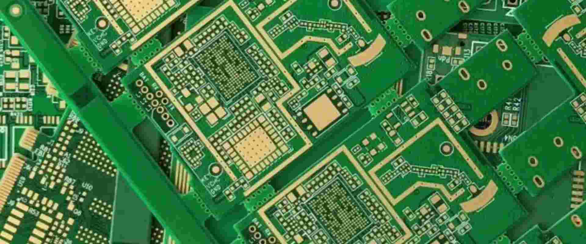
Layer Count Impact on Pricing

The number of layers dramatically affects manufacturing complexity and cost:

Cost Multipliers by Layer Count:

Why Layer Count Matters: Each additional layer requires separate lamination cycles, increased material usage, and more complex drilling processes. The manufacturing time increases exponentially with layer count.

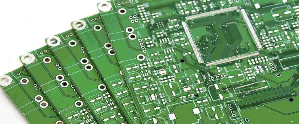
Board Size and Panelization Effects

PCB size directly impacts material usage and manufacturing efficiency:

Size Categories and Pricing:

  • Small (โ‰ค5ร—5cm): $3-10 per board (low volume)
  • Medium (5ร—10cm): $5-25 per board
  • Large (โ‰ฅ10ร—15cm): $15-50+ per board

Panelization Benefits: Proper panelization can reduce costs by 15-25% by:

  • Maximizing material utilization
  • Reducing handling time
  • Improving manufacturing efficiency

Manufacturing Process Costs

Standard Processes: Basic drilling, etching, soldermask application Advanced Processes: Controlled impedance (+15%), blind/buried vias (+25%), HDI construction (+40%)

Volume Pricing Structure

Understanding volume breaks is crucial for cost optimization:

Prototype Quantities (1-10 units):

  • Setup costs distributed across few units
  • $50-200 per board common
  • Focus on design validation over cost

Small Batch (25-100 units):

  • 40-60% cost reduction from prototype pricing
  • Sweet spot for testing market demand

Medium Volume (500-1000 units):

  • 60-70% cost reduction from prototype
  • Manufacturing efficiencies start to matter

High Volume (10,000+ units):

  • Maximum cost efficiency
  • 80-90% cost reduction from prototype pricing
  • Focus shifts to yield optimization

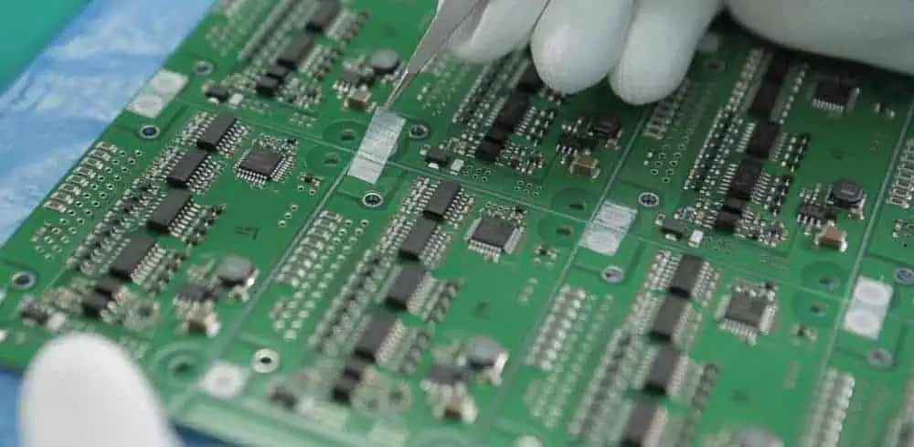
Assembly and Component Costs

PCB assembly (PCBA) represents a significant portion of total project costs, especially for complex designs.

Assembly Cost Components

Labor Costs:

  • SMT placement: $0.02-0.05 per component
  • Through-hole insertion: $0.05-0.15 per component
  • Hand assembly: $0.20-0.50 per component

Setup and Programming:

  • Stencil creation: $50-150
  • Pick-and-place programming: $100-300
  • AOI/testing setup: $100-500

Regional Cost Variations (2026):

  • China: Lowest cost, 2-4 week lead times
  • Eastern Europe: 30-50% higher than China
  • North America: 200-300% higher than China
  • Advantages of local assembly: Faster iteration, better communication, IP protection

Component Procurement Strategies

Cost-Effective Sourcing:

  • Use manufacturer-preferred parts (MPP) for 10-15% savings
  • Avoid obsolete or hard-to-find components
  • Consider alternative components with similar specifications

2026 Component Market Conditions:

  • Semiconductor shortage stabilizing but prices remain elevated
  • Passive component availability improving
  • Microcontroller lead times reduced to 8-16 weeks

10 Proven Strategies to Cut PCB Manufacturing Costs by 30%

Based on industry analysis and real-world case studies, these strategies can deliver significant cost savings:

1. Optimize Board Dimensions and Shape

Strategy: Design boards to fit standard panel sizes and avoid irregular shapes.

Implementation:

  • Use rectangular shapes whenever possible
  • Design to standard sizes: 50ร—50mm, 100ร—80mm, 160ร—100mm
  • Minimize board area while maintaining functionality

Real-World Example: A smart home device manufacturer reduced costs by 22% by changing their board from a custom L-shape (127ร—89mm) to a rectangular design (100ร—80mm), improving panelization efficiency.

Potential Savings: 15-25%

2. Reduce Layer Count Through Smart Routing

Strategy: Minimize layers by optimizing trace routing and component placement.

Implementation:

  • Use advanced routing techniques like differential pair routing
  • Consider component placement to reduce via requirements
  • Evaluate if high-speed signals really need dedicated layers

Tools and Techniques:

  • Use auto-routers for initial routing, then optimize manually
  • Implement length matching for high-speed signals
  • Consider trace width optimization for current-carrying capacity

Potential Savings: 20-35%

3. Standardize on Cost-Effective Materials

Strategy: Use standard FR-4 material unless specialty materials are absolutely required.

Material Selection Guide:

  • Standard applications: FR-4 TG130-140
  • High-temperature applications: FR-4 High-TG (TG170+)
  • High-frequency applications: Rogers only when necessary
  • Power applications: Aluminum core for thermal management

When to Upgrade Materials:

  • Operating temperatures >130ยฐC: High-TG FR-4
  • Frequencies >1GHz: Consider Rogers materials
  • High power density: Aluminum core or copper core

Potential Savings: 10-40%

4. Leverage Volume Purchasing Power

Strategy: Plan production runs to hit volume break points.

Volume Planning:

  • Analyze annual requirements to determine optimal order quantities
  • Consider shared tooling costs across product variants
  • Plan for inventory holding costs vs. unit cost savings

Joint Purchasing Opportunities:

  • Coordinate with other teams for combined orders
  • Consider component kitting services
  • Evaluate manufacturer partnership programs

Potential Savings: 30-60%

5. Simplify Surface Finishes and Specifications

Strategy: Use basic surface finishes unless specific requirements dictate otherwise.

Surface Finish Comparison:

  • HASL (Lead-free): Lowest cost, suitable for most applications
  • OSP: Good for fine-pitch components, limited shelf life
  • ENIG: Premium cost but excellent for HDI and fine-pitch
  • Immersion Silver: Good middle ground for performance/cost

Specification Optimization:

  • Use standard copper thickness (1 oz) unless higher current required
  • Relax tolerance requirements where possible
  • Avoid gold fingers unless required for card-edge connectors

Potential Savings: 10-25%

6. Optimize Via Strategy

Strategy: Minimize expensive via types and reduce overall via count.

Via Cost Comparison:

Design Guidelines:

  • Use through-hole vias whenever possible
  • Minimize via-in-pad requirements
  • Consider via stitching only where necessary for thermal/EMI

Potential Savings: 15-30%

7. Implement Design for Manufacturing (DFM) Principles

Strategy: Design with manufacturing constraints in mind from the start.

Key DFM Guidelines:

  • Maintain minimum trace widths (4 mil for most manufacturers)
  • Use standard drill sizes (0.2mm, 0.25mm, 0.3mm increments)
  • Provide adequate copper-to-edge clearance (0.5mm minimum)
  • Design for standard assembly processes

DFM Checklist:

  • Component orientation for automated assembly
  • Fiducial marker placement
  • Test point accessibility
  • Solder mask and silkscreen requirements

Potential Savings: 10-20%

8. Strategic Timing and Lead Time Management

Strategy: Plan orders to avoid rush charges and leverage standard lead times.

Lead Time Options:

  • Standard (15-20 days): Base pricing
  • Expedited (7-10 days): 25-50% premium
  • Rush (3-5 days): 100-200% premium

Timing Strategies:

  • Plan prototypes 6-8 weeks before needed
  • Schedule production runs during manufacturer off-peak periods
  • Consider partial shipments to manage cash flow

Potential Savings: 20-50%

9. Component Selection and Standardization

Strategy: Choose components based on availability, cost, and assembly efficiency.

Component Guidelines:

  • Prefer 0603 and 0805 packages over smaller sizes when possible
  • Use manufacturer preferred parts (MPP) lists
  • Avoid single-source components
  • Consider component lifecycle and availability

Cost-Effective Component Selection:

  • Standard resistor/capacitor values cost less
  • Popular IC packages have better pricing
  • Through-hole components for prototypes, SMT for production

Potential Savings: 15-25%

10. Supplier Relationship and Contract Optimization

Strategy: Build strategic relationships with manufacturers for long-term cost benefits.

Relationship Building:

  • Establish preferred vendor agreements
  • Negotiate volume-based pricing tiers
  • Consider partnership arrangements for design support

Contract Optimization:

  • Annual purchase commitments for better pricing
  • Flexible delivery schedules
  • Shared NRE (Non-Recurring Engineering) costs

Value-Added Services:

Potential Savings: 10-30%

Advanced Cost Optimization Techniques for 2026

AI-Driven Design Optimization

Modern PCB design tools now incorporate AI to suggest cost-optimal layouts:

AI Capabilities:

  • Automatic trace routing for minimal layer count
  • Component placement optimization for assembly efficiency
  • Real-time cost feedback during design process

Implementation:

  • Use AI-powered CAD tools like Altium Designer 24+
  • Implement design rule checks for cost optimization
  • Leverage machine learning for component selection

Supply Chain Diversification

The global supply chain disruptions of recent years have taught valuable lessons:

Risk Mitigation Strategies:

  • Dual-source critical components
  • Regional supplier qualification
  • Inventory buffering for critical parts

Cost Implications:

  • Higher inventory costs offset by reduced shortage risks
  • Supplier diversity may increase unit costs but improve reliability
  • Local sourcing provides better supply chain visibility

Sustainability and Cost Synergies

Environmental considerations increasingly align with cost optimization:

Green Manufacturing Benefits:

  • Reduced material waste through better panelization
  • Energy-efficient processes lower overhead costs
  • Recycled materials often cost less than virgin materials

2026 Sustainability Trends:

  • Bio-based substrates becoming cost-competitive
  • Lead-free processes are now standard
  • Halogen-free materials for electronics applications

Regional Cost Analysis and Manufacturing Trends

Asia-Pacific Manufacturing Hub

Advantages:

  • Lowest labor costs
  • Mature supply chains
  • High manufacturing capacity

2026 Developments:

  • Automation reducing labor cost advantages
  • Quality improvements closing gap with Western manufacturers
  • Lead time advantages due to proximity to component suppliers

North American Reshoring Trends

Driving Factors:

  • Supply chain security concerns
  • Reduced shipping costs and lead times
  • Government incentives for domestic manufacturing

Cost Implications:

  • 2-3x higher manufacturing costs
  • Faster iteration cycles
  • Better IP protection

European Manufacturing Focus

Strengths:

  • High-quality manufacturing
  • Strong automotive and industrial focus
  • Advanced technology adoption

Market Position:

  • Premium pricing for specialized applications
  • Focus on high-reliability and aerospace markets
  • Growing sustainability requirements

Technology Trends Impacting PCB Costs in 2026

Advanced Manufacturing Technologies

Additive Manufacturing:

  • 3D-printed PCBs for rapid prototyping
  • Reduced tooling costs for complex shapes
  • Limited to simple applications currently

Embedded Components:

  • Components integrated into PCB substrate
  • Reduced assembly costs
  • Higher initial PCB costs but lower overall system cost

Next-Generation Materials

Novel Substrates:

  • Graphene-enhanced materials for thermal management
  • Bio-based alternatives to traditional FR-4
  • Ultra-low-loss materials for 5G/6G applications

Cost Impact:

  • Premium pricing initially
  • Volume adoption driving costs down
  • Performance benefits may justify higher costs

Industry 4.0 Integration

Smart Manufacturing:

  • Real-time cost tracking and optimization
  • Predictive maintenance reducing downtime
  • Quality improvements reducing rework costs

Digital Twin Technology:

  • Virtual prototyping reducing physical prototype needs
  • Process optimization through simulation
  • Better yield prediction and cost forecasting

Future Outlook: PCB Cost Trends Through 2030

Market Projections

The global PCB market is projected to reach $106.85 billion by 2030, growing at a CAGR of 4.87%. Several factors will influence cost trends:

Growth Drivers:

  • Electric vehicle adoption requiring high-performance PCBs
  • 5G infrastructure buildout
  • IoT device proliferation
  • Medical device advancement

Cost Pressures:

  • Raw material price volatility
  • Environmental compliance costs
  • Labor cost increases in traditional manufacturing regions

Technology Roadmap

Near-term (2026-2027):

  • Increased automation in assembly processes
  • Better material utilization through AI optimization
  • Standardization of advanced processes

Medium-term (2028-2030):

  • Widespread adoption of embedded component technology
  • Significant cost reduction in HDI manufacturing
  • New substrate materials becoming mainstream

Strategic Recommendations

For Engineers:

  • Stay current with design tools incorporating cost optimization
  • Build relationships with manufacturing partners
  • Consider lifecycle costs, not just initial manufacturing costs

For Procurement Teams:

  • Develop supplier partnerships for long-term cost stability
  • Implement supplier diversification strategies
  • Monitor technology trends for early adoption opportunities

For Business Leaders:

  • Invest in design optimization tools and training
  • Consider vertical integration for high-volume products
  • Plan for supply chain resilience alongside cost optimization

Conclusion: Maximizing Value in PCB Manufacturing

Effective PCB cost management in 2026 requires a holistic approach combining smart design decisions, strategic supplier relationships, and awareness of market trends. The 10 strategies outlined in this guide can deliver substantial cost savingsโ€”often 30% or moreโ€”without compromising quality or performance.

Key Takeaways:

  1. Use modern PCB calculators with AI-powered features for accurate cost estimation
  2. Optimize design early to minimize layers, board size, and manufacturing complexity
  3. Leverage volume purchasing to achieve significant unit cost reductions
  4. Build strategic supplier relationships for long-term cost benefits
  5. Stay informed about technology trends that may offer cost advantages

The PCB manufacturing landscape will continue evolving rapidly, with new technologies and market forces reshaping cost structures. By implementing these strategies and staying adaptable to change, you can maintain competitive advantage while controlling costs.

Whether you’re designing your first prototype or optimizing production runs, remember that small design decisions can have massive cost implications. Start with a comprehensive cost analysis using modern calculators, then apply these optimization strategies systematically to achieve the best balance of performance, quality, and cost for your specific application.

Take Action Today:

  • Use a modern PCB cost calculator to baseline your current designs
  • Identify the top 3 cost optimization opportunities for your projects
  • Engage with manufacturing partners to discuss volume pricing and DFM guidelines
  • Plan your 2026 PCB requirements to leverage volume purchasing opportunities

The combination of smart design decisions, strategic planning, and modern tools can transform your PCB costs from a budget constraint into a competitive advantage.

Hot Tips for Excellent Prototype Board Soldering

PCB prototype assembly suppliers

Are you an engineer who wants to learn how to solder prototype boards in-depth? If so, you’ve arrived at the ideal location. Although soldering isn’t easy, you’ll be an expert with the appropriate advice in no time. This article covers the various solder types available for prototype board soldering, their benefits, and the two main methods for making solder joints and electrical connections between components.

What is Prototype Board Soldering?

Prototype board soldering is a procedure of connecting circuit components to a prototype board. Before committing to a complete production run, the engineer must test the design on a prototype board, normally a printed circuit board (PCB). It is versatile and simple to alter. This capability is ideal for prototype designs that might need modifications during the development phase.

Types of Solder

When soldering a prototype board, using the right type of solder is important. There are threeย types of solder commonly used for prototype boards, namely:

1.ย Lead-Free Solder

Lead-free solder aids in forming electrical connections between parts and comprises metals other than lead. Since lead is poisonous and needs to stay out of the environment, lead-free solder is becoming increasingly common in the electronics industry. Tin-copper and tin-silver-copper (Sn-Ag-Cu or SAC) are the two primary forms of lead-free solder (Sn-Cu). The average melting points of tin-copper and tin-silver solder are roughly 183ยฐC (361ยฐF) and 217ยฐC (423ยฐF), respectively. Moreover, it has a higher viscosity and needs a hotter soldering iron to melt it. On the other hand, lead-free solder is unsuitable for all soldering applications since it is weaker and more brittle than lead-based solder.

Lead-free solder consists of metals that are stable and non-toxic, making it safer for the environment than lead-based solder. Lead-free solder is often helpful in applications requiring high reliability, such as aerospace, military, and medical electronics. It is also widely applicable in consumer electronics, automotive electronics, and printed circuit boards.

Advantages

The following are some of the main advantages of Lead-free solder:

  • Environmental friendliness: Lead-free solder is a better choice than lead-based solder in terms of environmental friendliness. Lead is a hazardous chemical that can harm human health and the environment. The Lead-free solder eliminates the possibility of lead contamination, and PCB assembly has a smaller environmental impact.
  • Greater Reliability: This solder is more reliable than lead-based solder in terms of durability. It is more suitable for usage in tough conditions since it can sustain higher temperatures and is more resistant to thermal stress. It is, therefore, a dependable choice for long-term use.
  • Better Electrical Conductivity: Lead-free solder is more electrically conductive than lead-based solder. It lowers the possibility of electrical resistance and can enhance the device’s overall performance.
  • Improved Solder Joint Strength: Lead-free solder offers a stronger connection than lead-based solder, which makes it less likely to break or fail over time. As a result, the gadget is more durable overall.
  • Improved Surface Finish: Lead-free solder produces a better surface finish on the PCB, perfect for high-frequency applications. The device’s performance may improve due to the lower signal loss or interference likelihood of the smoother finish.

2.ย Flux-Based Solder

FULL PCB MANUFACTURING Quote

ย Flux is a chemical substance that aids in lowering the solder’s surface tension and preventing oxidation. While soldering, flux helps ensure that the solder, the component, and the board make a solid bond.

There are several types of flux, including liquid, no-clean, and rosin. The most popular flux used in soldering is rosin flux, which normally consists of rosin, ethanol, and water. Engineers use rosin flux when soldering components to prototype boards to guarantee that the solder creates a strong bond with the component and board.

Prototype board soldering also uses liquid flux, commonly comprised of water, ethanol, and boric acid. When soldering components on prototype boards, liquid flux helps lower the solder’s surface tension and stop oxidation. In addition, no-clean flux is another type of boric acid and water. It is not necessary to clear off no-clean flux after soldering because it aids in lowering the surface tension of the solder and preventing oxidation. No-clean flux is equally helpful in soldering components to prototype boards as the other two types.

Advantages of Flux-Based Solder

Employing flux-based solder comes with the following merits:

  • Improved soldering: Flux-based solder aids in cleaning and preparing surfaces for soldering, which results in better soldering. This feature lowers the possibility of voids or weak solder junctions and increases the solder’s stickiness. Moreover, flux-based solder aids in avoiding oxidation, which can lessen the likelihood of failure over time.
  • Reduced Heat Damage: Flux solder aids in equal heat distribution, lowering the possibility of heat-related component damage. This solder paste is crucial when working with fragile or sensitive components easily destroyable by high temperatures.
  • Decreased Soldering Time: Flux-based solder helps speed up attaching components to PCBs. Flux aids in surface cleaning and preparation, minimizing the need for extra cleaning or preparation stages.
  • Improved joint strength: Flux-based solder produces a stronger bind than unsoldered joints, enhancing the strength of the solder joint. This aspect increases the device’s general longevity and lowers the possibility of failure.
  • Decreased Solder Bridge Risk: Solder bridges, which can result in short circuits and other issues, can be easy to avoid with flux-based solder. This possibility lowers the probability of the item’s damage and enhances overall performance.

3.ย Lead-Based Solder

The lead-based solder consists of a large lead content. Electronics manufacturers have long used lead-based solder, but recent years have seen a decline in its use due to safety and environmental concerns. Despite its drawbacks, lead-based solder has benefits, such as soldering prototype circuit boards.

Lead and tin are the primary ingredients in lead-based solder, though other metals, such as copper, can also be part of it. Manufacturers may vary in their specific formulations for lead-based solder. Still, it normally contains either a lead-silver or a lead-tin alloy (often called “lead-tin” solder).ย Lead-tin solder typically has a melting point of around 183ยฐC (361ยฐF), while lead-silver solder typically has a melting point of about 230ยฐC (446ยฐF).

Benefits of Lead-Based Solder

The Lead-based solder may not be environmental-friendly. However, the following are some of its advantages:

Low Cost: Lead-based solder is an appealing alternative for applications that are on a tight budget because it is very inexpensive.

High Melting Point: Lead-based solder can be more suitable for high-temperature applications since it melts at a greater temperature than lead-free solder.

Stronger joints: Lead-based solder produces a strong link between components, increasing the device’s overall endurance. This feature leads to improved solder joint strength.

Excellent Electrical Conductivity: Lead-based solder provides superior electrical conductivity, which can enhance the device’s functionality. In comparison to other forms of solder, it is also less prone to result in electrical resistance.

Soldering Techniques

Soldering is a skill that requires practice and patience. Several techniques can helpย ensure that yourย components areย in their correct position.ย The following are two of these processes:

1.ย Hand soldering

The hand soldering process involves using a soldering iron, flux, and solder to link two or more components on a prototype board. Hand soldering is a typical technique to create electrical connections and solder joints between printed circuit boards, components, or cables. For reliable and high-quality solder joints, the hand soldering procedure needs a high level of ability and experience. Although it is ineffective for soldering several components at once, it offers great control and flexibility over the soldering process, making it perfect for small-scale production and prototyping.

The soldering Process

The process involves the following steps:

  1. Preparation: The Board and components must be ready before beginning the hand soldering process. Cleaning the PCB and the elements is necessary to eliminate any dirt or debris that can get in the way of the soldering operation. Before beginning, the operator should inspect the Board and the components for any damage or faults.
  2. Flux application: The operator adds flux to the PCB’s regions where the components will go. Flux is a chemical substance that aids in cleaning the PCB and component surfaces and enhances the solder’s wetting to form a solid bond.
  3. Component placement: The operator then adheres the components to the PCB, ensuring they are in their correct positions and with the proper orientation. The tweezers assist the operator in holding the elements in place to prevent them from moving while soldering.
  4. Soldering: This step involves heating the joint between the component and the board using the soldering iron. The solder flows around the connection and forms a solid link between the element and the Board when the solder melts due to the heat. The user must, therefore, be cautious not to apply too much heat since this could harm the PCB or the components.
  5. Board Inspection: After soldering, the operator should check each connection to ensure it is correct and free of flaws like solder bridges or cold joints. Before moving on to the following component, he should fix any of these errors.
  6. Cleaning: The operator should clean the PCB after soldering all the components to eliminate any flux residue or other debris that could affect the performance of the final product.

2.ย Reflow Soldering

This technique involves using a soldering iron, solder, and flux in a controlled environment to attach two or more components to a prototype board. The engineer initially heats the components to a temperature just above the solder melting point in this procedure. Often, a soldering iron or hot air rework station helps this. Next, he covers the prototype board with solder after assembling the components. Due to its effectiveness and dependability, reflow soldering is a widely used soldering technique in the electronics manufacturing industry. It makes producing circuit boards in large quantities with uniform and excellent solder connections possible.

The soldering Process

The reflow soldering process typically involves the following steps:

  1. Stencil printing: A stencil helps apply solder paste to the board. The stencil ensures that the paste only sits where the components will go.
  2. Component placement: After that, please put the components where they should be on the board.
  3. Preheating: Heat the board until you have activated the solder paste’s flux. The flux aids in cleaning the board’s and components’ surfaces of any oxidation or contaminants.
  4. Reflow: After raising the board’s temperature, the solder melts and flows, securing the components to the board.
  5. Cooling: To finish the soldering process and harden the solder, cool the board.

Conclusion

Soldering prototype boards is a crucial stage in the production of electronics. Lead-free solder, flux-based solder, and lead-based solder are the three types of solder most frequently used for prototype circuit boards. Each solder has benefits and drawbacks of its own. Therefore, selecting the appropriate solder for the task is critical. Moreover, components can be easily attached to a prototype board using one of the two primary soldering methods: hand soldering or reflow soldering. Engineers may confidently solder their prototype boards and start their projects with this knowledge. Thus, don’t think twice and start working with your soldering iron. After all, the easiest way to learn to solder is to get in and start getting your hands dirty.

What is a PCB Transistor and How Can You Test it?

transistors

Before you can comprehend how a PCB transistor functions, you must first understand what a transistor is and what to check for when choosing one. Before you purchase a PCB transistor, you must learn how you should test one.

What is a PCB Transistor?

Transistors are electronic devices that regulate the flow of electrons and hence regulate electricity. It implies they are in charge of initiating and terminating the electric current flow. Its main function is switching as well as enhancing the quantity of electronic impulses passing via circuit boards.

PCB Transistor Types

PNP and NPN are the two distinct kinds of transistors, and each has a different circuit symbol. Each of both transistors, which are built of semiconductor materials, has a unique set of layers. NPN silicon transistors, which are the simplest to produce, are the most widely used transistors.

Any novice must always begin by understanding NPN since they’re the simplest to comprehend. If you comprehend the NPN, it’ll be simple to help you study the full transistor and its various varieties.

How to Read PCB Transistors

transistor Component

NPN and PNP are the two most prevalent varieties of transistors, yet all of them can be made in many ways and are unique. Learning about transistors and understanding how to interpret a PCB transistor are the initial steps. Once you have mastered reading, then the next step for you is learning ways of testing them.

Our article would explain and teach you through the process involved in the reading a PCB transistor.

It is crucial to test the transistors so you can determine whether they will be helpful or not. Start by locating the marking beneath or close to the transistor.

  • Search for a line, an arrow, or a triangle with sides as well as a line beneath that appears to link them.
  • Unless the PCB transistor lacks that line, use that line which comes out from the left like the base. The metal enclosure acts as a foundation in the event that such a line is absent.
  • The transistor should be positioned so that the line that comes out faces the left hand side.
  • Be sure to locate and highlight the triangle since this NPN collector would be pointed upward and your PNP collector would be pointing below.

Testing the PCB Transistor

FULL PCB MANUFACTURING Quote

In circuits, transistors play a crucial role, thus it’s crucial to make sure they’re functional. When they are flawed, the circuit fails as a result. Because of this, it is crucial that you test them in order to make sure they are operating as intended. Be sure you understand what is expected of you before you start the procedure. A step-by-step tutorial for testing a PCB transistor is provided here.

Step 1

Before testing your transistor, make sure that there’s no electricity flowing through the circuit by ensuring it is switched off.

The battery should then be removed after unplugging its AVC power connection. Make sure that there’s no power present on the circuit board before simultaneously touching a capacitor’s two terminals with any metal. To prevent turning off stored power, use the screwdriver with insulation at the handle end.

Step 2

Watch out for the transistor that you will be testing for its collector, base, as well as emitter leads. These leads on some transistors are labeled for simple identification. C B, E, and B will be imprinted on them. By being certain of the orientation of leads, you should request a catalog from your electronics supplier. You should have confidence because the placements of the points vary depending on the transistor.

Step 3

If your digital multimeter has the diode setting, use it in this step; if not, use ohms setting. If the transistor is operating in the analog environment, set it using a low ohm scale.

Step 4

Touch a lead from of the meter into a base lead whilst you place its other on your collector lead to check the reading of the collector in both base-collector directions. Review the reading then share your advice. The transistor would display a reading for one direction as well as infinity for the other if it is functioning properly.

Step 5

While touching a lead towards the base while the other connects to an emitter, you must check the reading of the emitter on its base in the two directions.

Reverse these leads to read the meter in an opposite direction after checking it. Similar to step four, anticipate one reading should display 600 while the other will show an unlimited number.

Step 6


PCB Transistor
PCB Transistor

Remove its base lead if the reading isn’t really near to 600 because other components might be affecting the reading. Disconnect the data from the PCB by melting its solder attaching its base lead onto it. Using the meter, check both routes from of the base towards the collector-base towards the emitter. When you’re done taking the reading for the meter, melt your solder, push this lead into the hole of the board, and then reinstall it.

Step 7

Here comes the last step. Following testing, you ought to be able to tell if the collector or base-emitter readings indicate 0 in the two directions or if both indicate endless tasks. Zeros indicate a brief period of time. Moreover, infinities are signs of the open transistor diode.

However you are welcome to look here if you’d like to know more regarding how to thoroughly inspect a circuit board.

Conclusion

Prior to making a purchase of a PCB transistor, you must be aware of the transistor that you intend to utilize. In order to ensure that you’re getting the best open that suits you out of the many variations on the market, you must take care of a few things. The majority of providers will classify transistors based on their intended usage or the power rating.

In addition, if you don’t know much or are unfamiliar with pcb transistors, then it is crucial to speak with a professional to avoid making a mistake.

Things to you need to know about Unitech PCB โ€“ A Quality PCB Manufacturer

Shengyi S1000h PCB

If you’re unfamiliar with Unitech Corporation, you might wonder about its reputation. Established in 1994 by Chinese tech entrepreneurs, the company has diversified its business to include solar panels. In this article, we’ll delve into its history & current operations, as well as explore its offerings of rigid-flex printed circuit boards & double-sided printed circuit boards. By the end of this piece, you should be able to recognize a Unitech printed circuit board and understand how it can benefit you.

Solar cell business unit

Unitech Corporation will make more money by separating its solar cell enterprise into a new company. However, there was a report that Unitech’s founders took money from people who bought homes for other things. A giant electronics maker from Taiwan, called Inventec, is also a part owner of the new company. We don’t know how much money the new business will make yet, but there are some signs that it might be successful.

Chinese companies that make solar panels must reduce how much they produce, or they will keep losing money. Also, a new administration might focus on more reliable industries than solar. Lastly, the company might have to stop making solar panels because they don’t have enough money. However, this could be good for solar panel makers in Taiwan.

Multilayer PCBs

nanya-pcb-material

Multilayer PCBs by Unitech are gaining popularity in numerous industries due to their lightweight construction and impressive functionality. These boards are helpful in various high-tech applications, including X-ray equipment, optical fiber sensors, atomic accelerators, & weather analysis devices. Multilayer printed circuit boards offer several benefits to both manufacturers & end-users, including budget savings and improved functionality. 

Multi-layer printed circuit boards, with their increased number of layers, require more design time and attention during manufacturing due to their complexity. Any imperfection can render multi-layer printed circuit boards unusable. However, the benefits of using these boards are significant. They are more effective than single-layer printed circuit boards and can withstand a range of humidity, temperatures, & pressure. Additionally, flexible multi-layer printed circuit boards are helpful for assemblies that require flexible construction methods or applications that involve bending. 

With the increasing complexity and miniaturization of electronics, the internal elements must keep up with the trend. Double-sided printed circuit boards have proven insufficient in achieving a balance between size & functionality. However, multi-layer PCBs can overcome these challenges effectively. Unitech’s multi-layer printed circuit boards provide an ideal solution to meet this requirement, offering numerous advantages over traditional alternatives. Below are some benefits of utilizing multi-layer printed circuit boards. 

Multilayer printed circuit boards are strong and protected, making them great for putting lots of electronic parts close together. The coatings are connected well and help control how electricity moves through the board. This lets people do more things with the board and saves money because it’s easier to put many parts on it. 

Unitech’s multi-layer circuit boards are beneficial for cars. They can handle hot and wet conditions well and are solid and trustworthy. They also follow safety standards for the environment.ย 

Rigid-flex PCBs

FULL PCB MANUFACTURING Quote

Unitech PCB is growing because more people want to buy electronics for cars and everyday life. They are making more “rigid-flex” circuit boards to meet this demand, which they think will help them send out many circuit boards to people who make electronics. They are also planning to use these circuit boards for phone parts and are working with other important circuit board companies like Rayming PCB and Assembly. 

The new circuit board called a “rigid-flex printed circuit board,” has parts that are both hard and bendy. When it gets hot, it won’t get more extensive in some directions. This circuit board is better than other types because it doesn’t use things that get bigger or wet. They usually make these boards with stuff like sticky glue and a special kind of plastic that bends. However, these materials can make the board more extensive and cost more money. 

Rigid-flex circuit boards benefit space and car technology because they make things more robust and reliable. They also eliminate the need for breakable wires and connections made with melted metal. People can use them in testing machines, tools, and cars too. So if you need a circuit board that can handle being hit, shaken, or put in hot or cold places, a rigid-flex board is a good choice. 

Rigid-flex circuit boards cost more to create, but they save money when being made. This is because they can fit lots of parts on one board, so you don’t need to use lots of boards. This is cheaper. They can also be made special for different things and fit into different shapes. They are suitable for trying out new ideas because they are easy to test, even if they need to be small.ย 

Double-sided PCBs

double layer pcb circuit board

Unitech PCB Corp. is a company from Taiwan that makes circuit boards & solar panels. They make circuit boards that have circuits on both sides and also ones with lots of layers. They also make a particular solar panel called a “mono-crystalline silicon” panel. You can find their things in many places in Asia. If you want to know about their circuit boards, click the links below. 

Many circuit boards only have circuits on one side, which means you can only put parts on one side too. But using a “double-sided” panel, you can put pieces on both sides. This is good because it makes the board smaller and takes up less space. When the board is being made, they can also put more metal on it, which can help it handle heat better. This means the board can be even smaller and cheaper to make. 

Single-sided & double-sided circuit boards both have good things about them, but they aren’t identical. Double-sided boards are harder to make because you must put parts on both sides. This makes it cost more money to make. If you don’t have much money, you might want to use a single-sided board instead. This will be cheaper but may not be as flexible as needed for your job. 

A single-sided PCB has metal lines on one side and is more affordable than double-sided boards. They are often used in things like electronics for regular people and factories. You can also order a “flexible” version of the board. This board is made from a flexible material, so you can bend it without breaking it.

Future of Unitech PCB

Unitech PCB has become more successful since it started. Customers & shareholders wonder how it will keep growing in the future. Many things make a business successful, so there isn’t just one answer. Unitech PCB has plans and a direction that links each project together. The business’s future looks good – what about yours? 

Panasonic has announced that it will start making OLED television screens in 2020 at its factory in New Zealand’s Marlborough region. The manufacturing process will use both Japanese & Chinese techniques. 

Conclusion

Unitech PCB is a company from Taiwan that specializes in making PCBs. Their goal is to offer high-quality products that are valuable to their customers. Unitech has many client options, like rigid-flex printed circuit boards, flexible printed circuit boards, and printable boards. They also allow you to choose the best PCB that fits your product. 

Top Low-Cost PCB Manufacturing Companies & Benefits

hot swappable PCB

The time, money, and manpower needed to create a PCB are only a few resources. This makes the PCB costs vary with respect to these factors. Circuit boards are sold at competitive costs by PCB manufacturers and suppliers. It’s natural for people to choose the more economical choice because the price is a significant component of the process of decision-making when choosing a PCB maker.

PCBs with short turnaround periods are emphasized by cost-effective PCB manufacturers, who offer effective PCBs at a price suitable for most consumers. Their mission is to provide top-quality PCBs at a reasonable price. Let’s explore the issue of making PCBs more inexpensive in more detail.

What Is Low-Cost PCB Manufacturing?

An economic PCB provider offers PCB manufacture at a low price. High-quality printed circuit boards are produced by this source at a reasonable cost. Budget-friendly PCB vendors provide PCBs that adhere to the highest standards of quality set by the industry. These PCBs go through extensive testing. Hence, a key component of a cost-effective PCB manufacturing process is quality assurance. You may choose from a variety of PCB types that are both high-quality and reasonably priced. You may get complex circuit boards from a cost-effective PCB provider at a price that is both reasonable and up to par in terms of quality.

It’s crucial to understand that “cheap” circuit boards do not necessarily mean lower quality. The goal is to reduce production costs without sacrificing quality. Each PCB is put through rigorous testing to make sure it meets quality requirements. Low-cost PCB makers make sure their products adhere to all quality requirements set by the industry.

Factors To consider while Choosing a Low-Cost PCB Manufacturing Company

portable pcb

Although all PCB providers can construct PCBs, there may be differences in technology and procedures. So, it’s important to consider a few things when selecting a cheap PCB provider. The following are some things to bear in mind:

ยท Quality Control:

Predetermined procedures and protocols are the basis of quality control. It also includes automated systems that check each project carefully while it is being produced. Low-cost PCB vendors may guarantee quality through AOI and X-ray inspections. Additionally, PCB’s functionality may be verified using a variety of testing methods. These inexpensive producers aim to provide high-quality PCBs at a reasonable cost.

ยท Expertise:

Suppliers of inexpensive PCBs have established a reputation for quality. These producers use knowledgeable and experienced workers who have the training and credentials necessary for fabricating PCBs. Some manufacturers additionally create training courses for their staff to guarantee the right protocol is executed. Also, these low-cost PCB producers use cutting-edge machinery and follow a tried-and-true manufacturing technique.

ยท Flexibility:

The ideal low-cost PCB provider should be able to satisfy a variety of client requirements. Also, this manufacturer must be qualified to complete manufacturing runs. Also, this manufacturer must be able to offer several PCB kinds. A crucial consideration when choosing a cost-effective PCB provider is flexibility.

ยท Customer Assistance:

Choose a PCB provider that pays close attention to its client’s demands when you’re looking for one. It is crucial to select a manufacturer who puts the interests of the consumer first. The greatest PCB producers must provide their customers with the type of PCBs that are affordable.

Top 5 Low Cost PCB Manufacturing Companies

FULL PCB MANUFACTURING Quote

There are many low-cost PCB providers around the globe, but they do not all provide high-quality PCBs. Thus, it is crucial to locate the most affordable PCB providers.

1. ALLPCB:

ALLPCB ensures that high standards are reached while providing consumers with affordable PCB manufacturing. This expert maker of PCBs works hard to deliver high quality without sacrificing price. Clients are given a range of alternatives in terms of cost and lead times.

The customer’s happiness is also a top priority for the team of experienced engineers and technicians at ALLPCB. To make the purchasing process simple for customers, an open, user-friendly ERP system is offered.

Moreover, ALLPCB offers a variety of economical PCB solutions to pick from, professional help on speedy PCB production and assembly, and allows consumers to make purchases at a competitive price.

2. RayMing:

A respected company, RayMing, offers extremely affordable PCB manufacturing without sacrificing quality. To guarantee that high-quality PCBs are created at competitive prices, it employs tight quality control procedures throughout its production process. RayMing is a proper one-stop solution for all one’s PCB manufacturing needs.

It also provides expert advice on PCB assembly and production, everything you need to design the PCB and upload the Gerber files; RayMing will handle everything else. To assure effectiveness and quality, the company uses the most recent technology and production techniques.

RayMing collaborates with skilled engineers and technicians that are committed to offering high-quality goods at competitive pricing. You can count on RayMing to meet your demands for low-cost PCB manufacturing. Also, they provide fast lead times on their inexpensive PCBs. The RayMing staff uses a variety of tactics to lower the cost of PCB assembly because they understand how important it is to strike a balance between cost-effectiveness and quality.

3. Custom Circuit Boards:

The primary focus of Custom Circuit Boards is to provide PCB fabrication at incredibly low prices while upholding high standards of quality. An extensive selection of PCB solutions, including local and international printed circuit boards, are available from this American PCB firm, which also provides great customer service. To guarantee that quality is not compromised, a trained team of technicians and engineers collaborate closely.

Each sort of PCB you need may be found at Custom Circuit Boards; they are your one-stop store for all PCB demands. For those seeking more durable, reasonably priced PCBs, it is a fantastic option. Also, they provide low-cost PCB prototypes, during which their engineers carefully review your BOM to guarantee the components’ correct operation and stability.

To ensure high-quality products, this PCB producer employs rigorous control procedures throughout its production process. To identify and address design flaws, the organization uses the DFM assessment. Documentation control is heavily emphasized by Custom Circuits. Also, this renowned company produces circuit boards of the highest caliber using cutting-edge production methods.

4. PCBWay:

rogers substrate

One of the top low-cost PCB manufacturers in China, PCBWay has a great deal of experience in creating high-quality and affordable PCBs. This firm specializes in creating all sorts of printed circuit board PCBs at cheap pricing. Whether you need a PCB prototype or a medium-scale PCB, PCBWay has got you covered. 

In addition to offering full-day technical help, PCBway also provides inexpensive PCBs. PCBway provides the most inexpensive PCBs without sacrificing quality because of its abundance of professional and technical expertise.

The company offers services including board assembly, component sourcing, and manufacturing, making it a one-stop shop for cost-effective PCB manufacturing and PCB assembly. All of PCBway’s circuit boards are delivered after rigorous testing.

5. Sierra Technology:

Sierra Assembly Technologies is a leading manufacturer of inexpensive PCBs and understands the significance of cost control in the current industry. They place a great priority on cutting costs without sacrificing quality. They keep strict quality control procedures in place throughout PCB production to accomplish this.

For cost-effective PCB production, you may rely on the experience of this PCB manufacturer. They collaborate with experts that hold the required credentials for PCB production and have a great deal of experience in PCB creation. Their PCBs include RoHS-compliant and lead-free, making them a dependable option for low-cost PCBs.

Benefits Of Low Cost PCB Manufacturing Services

Worldwide, circuit board producers use a variety of methods to reduce costs while maintaining quality. PCB producers’ main objective is to keep prices down while maintaining the excellent quality of the boards they make.

Although some manufacturers are concerned with cutting costs, it doesn’t imply that the PCBs they make have subpar quality. The fact is that many companies that produce inexpensive circuit boards make an effort to make the most of their assets in hopes of manufacturing excellent boards.

ยท Low Labor Price:

Labor expense is one factor that affects the total cost of production. Labor expenses can significantly affect how much less expensive fabrication is when they are low. An illustration of this may be observed in PCB businesses in China, whereby labor expenses are remarkably low, and PCBs are sold for less money as a result.

ยท Advanced Technology:

Modern technology is used by companies that produce inexpensive circuit boards to reduce the expenses of manufacturing. In hopes of reducing the total cost of Printed circuit boards, these producers make investments in the newest production machinery. To further reduce expenses, they consistently enhance their production techniques.

ยท Low-Cost Materials:

The price of acquiring the different materials and components needed has an impact on the cost of PCB manufacture. It may be possible to reduce the overall cost of manufacturing by being able to purchase these things for less money. Several producers of inexpensive PCBs provide a whole service that involves sourcing components and materials, which means they take care of the duty of locating the resources required to create PCBs.

Conclusion

Technology improvements have helped to bring down production costs in the competitive industry of PCB fabrication. Lowering the costs of PCB manufacture is essential for remaining competitive. The production processes can be improved as a means of achieving this. The electronics sector has benefited from the adoption of low-cost PCB fabrication.

Top 10 Free Electronic Schematics Makers to Enhance Efficiency in Work

electronic schematics

In the past, electrical engineers relied on pen & paper to make circuit diagrams. However, with the rapid advancements in technology, the process of making diagrams has evolved. Today, we will be focusing on circuit diagram makers and how they have replaced the traditional methods of diagramming. Gone are the days when electrical engineers had to rely on pen and paper to draw circuit diagrams. With technological advancements, creating charts has become much easier and more efficient. Nowadays, there are various software programs available that offer advanced options for labeling, notation, and more, making it easier and faster to create electrical circuit diagrams. To help you out, we have compiled a list of 10 of the perfect circuit diagram creator tools you can explore. 

A circuit diagram is a drawing that shows how electrical components are connected. It uses symbols to represent different parts and uses a unique circuit diagram maker tool. By looking at the circuit diagram, you can see how everything is connected so the device works correctly. Each circuit component is represented by a unique icon that is globally recognized and conforms to industry standards. Thus, labeling is unnecessary, except for numerical values that may differ depending on the component’s intended function.ย 

Top Free Electronic Schematics Makers

Free electronic schematics

This section provides a brief overview of six of the most influential circuit diagram creators present in the market. While some of this equipment may have a cost associated with them, they offer pre-built symbols & icons that can save a significant amount of time when drawing complicated circuit diagrams that include multiple components and require the proper demonstration of relationships between them using lines (known as buses). 

1. GitMind

The first tool on our list is GitMind, a diagramming software that offers pre-designed symbols to assist users in creating circuits, flowcharts, UML diagrams, and more. It has various clipart options for making electrical circuits, or users can upload their own. Once the diagrams are complete, they can be exported in formats like PNG & PDF. The tool is compatible with most web browsers and can be used on Linux operating systems, Mac, and windows. It’s easy to use and navigate, even for those with less experience with the software.

2. EdrawMax

Consider using EdrawMax as another circuit diagram maker. Its interface is identical to Microsoft Office, making it user-friendly for those familiar with MS software. It also boasts a library of shapes suitable for both professional & educational purposes. In addition to creating circuit diagrams, EdrawMax can also create computer networking, org charts diagrams, architectural diagrams, UML diagrams, and more. 

3. SmartDraw

SmartDraw offers both an online edition and a desktop version for users who prefer offline access. While the online version is convenient, the desktop version can be helpful with limited internet connectivity. With a wide range of Predesigned templates, SmartDraw helps accelerate the creation of circuit diagrams from simple to complex. However, compared to other similar programs, its cost may be relatively high. 

4. Visual Paradigm

FULL PCB MANUFACTURING Quote

The following program on our list is a lucid chart, which can be used both online and offline with its desktop and browser-based editions. It provides a wide range of Blueprints that can be freely edited, making it a fascinating tool. The categories in this online circuit creator are arranged alphabetically, making it easy for you to find specific Blueprints. You can customize the font size, style, shape, color, and more elements. Another noteworthy feature of Visual Paradigm is its video conference function, which allows for effective collaboration and communication with other group members.

5. CircuitLab

CircuitLab is a specialized program designed exclusively for creating circuit diagrams. One of its noteworthy features is the ability to run simulations to verify the accuracy and correctness of the components & connections. It makes this analysis process much quicker and more efficient, ultimately saving time & money that would have been spent on practical approaches. Regrettably, this diagram maker can only be accessed through the web. Therefore, no desktop version would allow you to use it offline. However, it can be used on popular web browsers such as Edge, Chrome, and Firefox if you have a good internet connection. 

6. CircuitMaker

CircuitMaker is another reliable option for creating expert circuit diagrams. With this tool, you can freely edit PCBs without any dimension or layer restrictions. Additionally, you can build up to five projects and choose to share them with communities or selected users and authors. One of the top circuit design software options available is equipped with Altium 3D PCB design technology, enabling a fully immersive 3D view of the printed circuit board layout. In addition to this cutting-edge feature, the software offers a range of other valuable tools, such as Shove routing and a multi-sheet editor. Overall, these features make it a top contender among circuit makers. Best of all, this powerful software is available for free. 

7. Lucidchart

Lucidchart is an excellent choice for creating various electrical diagrams, including circuit diagrams, due to its flexibility and versatility. It offers a broad range of industry-standard symbols and categories, such as transistors, resistors, and power sources, which enable a user-friendly experience for designing high-quality diagrams. It is no surprise that many prominent organizations, including GE, Cisco, & Whole Foods, trust this circuit diagram maker for their design needs. If you are searching for reliable software for creating circuit diagrams, Lucidchart is a top contender.

8. Schematics

The tool called Schematics is not limited to creating circuit diagrams only, as its name suggests. It can also depict machine components, a process, or a device, making it a versatile option for diagramming. In other words, the equipment helps draw both circuit and schematic diagrams. Additionally, circuit diagram makers feature standardized representations of electrical components, symbols, & configurations. It also allows for easy work with colleagues as all projects are shareable. Furthermore, the tool supports various popular platforms, such as Twitter & Facebook, making it accessible from multiple devices. 

9. EasyEDA

EasyEDA is a versatile tool that not only enables you to visualize and analyze circuit output but also facilitates collaborative circuit layout planning with your group. With 3D views, you can enhance the clarity and understanding of your diagrams. The tool offers extensive customization options for canvas attributes, routing angle, grid, and other design elements. Moreover, EasyEDA provides a wealth of pre-designed circuits and the ability to import designs from other platforms, making it an excellent choice for free circuit design software. 

10. Autodesk Eagle

Autodesk Eagle is an excellent application for individuals using PCBs, especially when working with complex semiconductor chips containing many electronic elements. Given the prevalence of such components in modern electronics, programs like Eagle have been highly sought after. One notable feature of this circuit diagram maker is its vast collection of printed circuit board layouts. Additionally, users can customize their designs with options such as loop removal, routing, and cornering. Another compelling aspect is the ability to incorporate 3D components into diagrams, leveraging the capabilities & possibilities of Fusion 360. 

Conclusion

These are the top ten diagram creators that can be used both online & offline. While each piece of equipment has unique features, they all share the common purpose of making circuit diagrams. However, to determine which tool is best suited for your needs, it’s recommended to try them out first-hand. 

In conclusion, with the abundance of circuit software available in today’s technological landscape, it can be overwhelming to choose the right one. Thankfully, the list of 10 simulations online equipment provides a great starting point. Not only are they completely free, but they can also be used directly from their respective websites. Depending on the level of expertise and specific requirements, you should be able to select an accurate simulator from the list provided above easily. Each tool has unique specifications that cater to different needs. If you require additional information or have any questions, please do not hesitate to contact us.

An Ultimate Guide About 1.8K Resistor

Resistors in Series

A 1.8k resistor is an electronic component with a resistance value of 1.8 kilo-ohms. This means that the resistor can resist the flow of electrical current through a circuit by 1.8 thousand ohms. It is a passive component, which means that it does not require any power source to operate. The 1.8k resistor belongs to the family of fixed resistors. So, it means that its resistance value is predetermined. We canโ€™t adjust its value. Several factors, such as the composition of the material and the physical dimensions of the resistor, affect its resistance.

What Is the Color Code of the 1.8K Resistor?

 Color codes made the identification of resistors easy. These are not decorative ribbons or lines. These color codes have a specific meaning. Every resistor has a unique color code that explains its resistance. Furthermore, you can easily distinguish between different resistors in a circuit with their color codes. Color codes are particularly useful in more complex circuits because there are many different types of resistors with similar physical appearances. So it is easy to get confused. Let’s have a look at the color code of the 1.8 k resistor.

A 1.8 k resistor typically has a color code of brown, gray, red, and gold.

  • The first brown band has the digit value 1.
  • The second gray band has a digit value of 8.
  • The third band is red in color. It is a multiplier band, and the multiplier value is 2.
  • The fourth gold band represents tolerance. Therefore, the color code for a 1.8 k resistor is brown, gray, red, and gold.

ย All bands have different values. It’s hard for a layman to recognize the color code. If you’re familiar with the basics of resistors, you’ll recognize this color code easily. That’s why you can use a 1.8 k resistor in your circuit design in a hassle-free manner.

How to Choose the Right 1.8 K Resistor for A Specific Application

THT Resistor
THT Resistor

1. Determine The Nominal Resistance Value

The nominal resistance value is the desired resistance of the resistor in the circuit. It is typically determined based on the specific requirements and specifications of the circuit, such as the desired voltage or current levels.

2. Consider Tolerance.

The tolerance of the resistor specifies the maximum deviation of the actual resistance value from the nominal value. A lower tolerance indicates a higher level of accuracy but may also increase the cost of the resistor.

3. Consider The Temperature Coefficient

Resistance values change with temperature according to the temperature coefficient of a resistor. When the resistor has a wide range of temperatures, a low-temperature coefficient is important. Sometimes it is related to heat dissipation.

4. Consider The Power Rating

Depending on its power rating, the resistor can dissipate a maximum amount of power without overheating. Many people ignore the power rating, and later they regret it.

5. Consider Other Specifications

Other resistor specifications such as frequency response, noise characteristics, and environmental factors. Choosing a resistor that meets these additional requirements can help ensure that the circuit operates reliably and accurately.

6. Choose The Appropriate Type and Package

Different types and packages of resistors are available, each with its own advantages and disadvantages. Through-hole resistors are easy to use and durable, while surface-mount resistors are smaller and more suitable for high-density circuits. Wire-wound and film resistors offer high accuracy but may be more expensive.

7. Verify Compatibility

Once a resistor has been selected, it is important to verify that it is compatible with the other components and specifications of the circuit. This may involve checking the maximum operating voltage and temperature, the frequency response, and other factors that can affect the performance and reliability of the circuit. Some resistors are incompatible with the other parts of a circuit. So there are several factors that you should keep in mind while selecting a compatible 1.8k resistor.

How to Make a 1.8K Resistor?

FULL PCB MANUFACTURING Quote

Making a 1.8k resistor from scratch requires specialized equipment and knowledge of the properties of the materials used to construct the resistor. However, it is possible to modify an existing resistor to achieve a 1.8k resistance value. There are a few things that you should keep in mind.

  • If you are going to design a complex circuit, then it would not be recommended to make a DIY 1.8 k  resistor.
  • Modifying a resistor sometimes doesn’t serve the purpose.
  • You may face voltage, heat dissipation, and noise issues due to the modification in the resistor.
  •  That s why it is always better to use a commercially manufactured 1.8 k resistor.

One method for modifying a resistor involves adding a second resistor in series or parallel with the original resistor. The resistance value of the second resistor can be selected to achieve a combined resistance value of 1.8k. For example, if you place a 1k resistor in series with an 820-ohm resistor, the combined resistance will be 1820 ohms. It is close to the desired 1.8k resistance value.

Another method for modifying a resistor involves trimming its resistance value. This process is known as the trimming process. This process involves selectively removing a small amount of the resistive material from the resistor using a laser. Sometimes it doesn’t provide the proper results.

However, these methods of modifying resistors are not good for general use. As a matter of fact, they can damage the resistor and affect its performance. Experts recommend purchasing resistors with the desired resistance value from reputable electronic component suppliers.   If you don’t follow the guidelines, then you have to compromise the circuitsโ€™ performance.

Conclusion

1.8k resistor is a common and useful electronic component. Its resistance value is practical for many different types of circuits. It can be helpful for voltage regulation, current limiting, signal processing, and more. Itโ€™s convenient to use, making it perfect for many electronic designers and hobbyists. Overall, the 1.8k resistor is an important component in electronic circuits. Its adaptability and compatibility with a wide range of applications make it an essential part of any electronic enthusiast’s toolkit.

All You Need to Know about Laser Print PCB

laser print pcb

PCB manufacture is an extremely difficult operation that needs highly specific tools and engineering knowledge. The use of lasers is among the most recent breakthroughs in how technology has simplified key components of PCB manufacture.

A variety of materials are needed for PCB construction. To ensure both electrical and mechanical dependability, these materials are chosen depending on their electrical performance. The PCB manufacturing process heavily relies on PCB laser engraving.

Lasers Marking In PCBs

Circuit board marking is a crucial phase in the production of PCBs, and PCB lasers are being utilized for this. Due to the complexity of electronics production, it is crucial to label boards to identify essential components and ensure that parts are positioned correctly for proper connection.

Identification markers have grown in importance in the manufacture of PCBs. Alphanumeric identification markers have been used in the past. However, there are limitations because of the size of the PCB surface. Since they can provide accurate marking, lasers are utilized to label Boards.

Each PCB surface may benefit from adding identification codes, and fiber laser Printed Circuit Boards can employ barcode technology and QR codes that fit more data into a given area.

Lasers can mark Boards quickly and efficiently. They can quickly etch codes while shielding the material all around the application region from deformation or damage. Information is also provided through laser labeling during the fabrication of circuit boards. Precision, efficiency, and accuracy are crucial in this application.

It’s also crucial to understand that marking components with lasers follows the same process as marking printed circuit boards. This ensures that delicate and fragile components are really not put under excessive pressure while making it simple to identify and replace components.

Lasers Cutting In The PCBs

Cutting is a crucial part of PCB fabrication because a PCB needs to be constructed using only a stencil with holes for connecting and soldering components. PCB stencils may be quickly and efficiently cut in bulk using a fiber laser. The material of the circuit board may be punched by using a laser-cut PCB beam to create the required perforations, protecting the material’s structural integrity around it.

This technique must be repeated several times when mass production is involved. As they employ a non-contact method to cut the PCB materials, CNC laser PCB reduces damage from happening and reduces waste. An essential component of PCB production is fr4 cut by laser.

Lasers Sintering In The PCBs

Sintering is regarded as the ideal approach for attaching PCB components because it may resolve the issues with soldering and allow stronger, more reliable connections to develop as PCBs are being made.

Laser sintering enables the production of creative PCBs without solder, which represents the future of printed circuit boards. This method permits greater stability and works well in high-density PCBs. A silver-containing powder is exposed to a laser during the sintering process. The powder is heated by the laser until it reaches a melting temperature, at which point it is given the opportunity to cool and solidify.

Laser Cutting For The PCB Depaneling

For PCB manufacturers, laser depaneling is a fantastic technique that can save both money and time. Circuit boards have delicate components that are prone to damage, and laser depaneling lessens the strain on these components and the solder links they share.

How To Select Laser Routing For Depaneling of PCB?

FULL PCB MANUFACTURING Quote

One common method for depaneling is laser routing. This process makes sure that the board is not touched directly. Several manufacturers believe that laser routing is suitable for the delicate and compact PCBs utilized by the newest wearable technology.

Two lasers are used for PCB depaneling: CO2 and UV. The most crucial elements to take into account when choosing the kind of laser to employ are the relative significance of processing times and the tidiness of the outer edges.

Choosing The Right Laser Source

For the depaneling needs, it’s crucial that you use the right laser source. The pros and cons of UV and Co2 lasers are described below.

ยท UV Laser:

The “Cold” cutting technique is used with lasers that employ UV light. UV lasers have made it simple to regulate the edge’s thermal charring. Hence, if eliminating char is more important than speed, a UV laser seems to be a superior choice.

The pros of using Uv Lasers include Low HAZ, provides tidy cuts, a very thin kerf width, and the capability to cut the leads of copper with accuracy.

However, it also has cons. It takes a long time to cut and is a little bit expensive. 

Several iterations of laser scanners are used to cingulate the Boards when using a UV laser in order to obtain clean cuts. Software controllers are used to regulating the cut speed. The entire paneling that cingulate the board is sliced through by these cuts.

ยท Co2 Laser:

If the time of the cycle is highly critical to you, a CO2 laser seems to be a better choice. CO2 laser Printed Circuit Boards are more frequently used to produce perforated cuts but may also assist in making entire cuts. Using the perforation technique lessens char while also making it simpler to load and unload boards and panels from the cutting process.

With the perforation technique, the space between perforations is crucial. Lesser char upon the outer edge will result from a larger space, but it will take more effort to divide the boards. Depending on the specified requirements, we may simply alter perforation strength.

Moreover, when material thickness grows, both cycle time and charring increase. Laser cuts may be quicker and cleaner if panels with V-grooves were manufactured at the cut areas.

The pros of using this laser source includes quick speed cuts, cutting the thicker substrates accurately, costing less for every watt, and also allowing the aluminum panels for processing.

It also contains some cons which is Larger HAZ, greater kerf width, and more charring.

How To Improve Cut Accuracy For Depaneling of PCB?

laser-cut-pcb

The precision of the cutting while depaneling PCBs is crucial for reducing damage and waste. You must make sure that the cut location is constant, and you can do this by making sure that the laser is precisely aligned with the panel’s features and components.

To guarantee that the cuts precisely correspond to the circuits, a vision system recognizes certain elements on the board and modifies the cut route.

Why Laser Depaneling of PCB Is Better Than Other Methods?

  1. A no-contact methodology is used in the technique of laser routing. Hence, there is no mechanical pressure on the components.
  2. No need to replace or sharpen worn-out blades
  3. may cut through any route, even bends
  4. Software adjustments that make it easy and rapid to switch between several cut patterns
  5. No mechanical components are changed, and the blades aren’t adjusted.

Laser Drilling In PCBs

To construct connections between several layers, laser drilling creates holes in a PCB. In modern houses, we have HDI boards that employ laser drills as electronic equipment. Drilling using a laser ensures precision even when dealing with tiny diameters.

For a hole to be drilled, laser drilling uses laser energy. Using a machine to drill holes is quite different from this. To place components and provide connections between different layers, holes are bored into PCBs. On the plain reinforced glass, lasers can drill vias that are 2.5 to 3 mils thick. For an unreinforced dielectric, it can drill around 1 mil vias.

Benefits Of Drilling PCB With A Laser

There are various advantages to utilizing lasers for drilling. Some of them are described below.

ยท Precise control: 

With the aid of lasers, you can better regulate the laser beam’s period, intensity, and emission of heat. This offers excellent precision and facilitates the creation of different hole shapes.

ยท Multi-Tasking:

Cutting, sintering, welding, and other manufacturing operations may all be done using lasers.

ยท No-contact Process:

Lasers guarantee a non-contact technique, thus vibration from drilling has no impact on the object being worked on.

ยท High Aspect Ratio:

An essential drilling hole parameter is the aspect ratio. The ratio of the hole’s diameter to its depth is known as the aspect ratio. Due to their ability to create holes with tiny diameters, lasers have a high aspect ratio.

Factors To Consider During Laser Drilling

fiber-laser-pcb

There are some factors that need to be taken into consideration while drilling with a laser. The main two factors are

ยท The copper Thickness:

The desired copper layer’s lowest thickness must be two times as thick as that of the topmost copper layer that will be drilled. The best method for creating micro vias in Printed circuit boards is with lasers. PCB manufacture relies on laser-drilled micro vias.

ยท Non-homogeneity Of The Stack-Up:

The stack-up non-homogeneity is crucial when drilling with lasers. Different materials absorb energy at different rates. For instance, the glass fibers and FR4 resin absorb energy at the same rate. Because glass vaporizes considerably more quickly than BT epoxy, glass fibers are left in the hole.

Conclusion

Lasers are crucial pieces of specialized machinery utilized in the production of PCBs. These tools serve the purpose of cutting, drilling, sintering, and marking PCBs, among other things. This technology is a better solution for PCB producers since it gives accuracy. Lasers also employ the no-contact method, making it simple to employ during PCB manufacturing. In the manufacture of PCBs, laser engraving is employed.

PCB Suppliers in Pakistan: Import Trends & Key Manufacturers (2025 Update)

china pcb board manufacturer

Introduction

The electronics industry in Pakistan has been experiencing significant growth in recent years, driven by increasing domestic demand and government initiatives to promote technology-based industries. As a crucial component of electronic devices, printed circuit boards (PCBs) play a vital role in this expanding sector. This article explores the landscape of PCB suppliers in Pakistan, analyzing import trends, key manufacturers, and the overall state of the electronics trade in the country as we look ahead to 2025.

The Growing Importance of PCBs in Pakistan’s Electronics Industry

Before delving into the specifics of PCB suppliers and importers, it’s essential to understand the significance of PCBs in Pakistan’s burgeoning electronics sector:

  1. Technological Advancement: PCBs are fundamental to the development of advanced electronic products.
  2. Economic Growth: The electronics industry contributes significantly to Pakistan’s GDP and export earnings.
  3. Job Creation: The PCB and electronics sectors provide employment opportunities for skilled workers.
  4. Innovation Hub: A robust PCB supply chain supports local innovation and entrepreneurship in electronics.

PCB Import Trends in Pakistan

Current State of PCB Imports

Pakistan relies heavily on imported PCBs to meet its domestic demand. Let’s examine the current trends:

  1. Volume of Imports: The country has seen a steady increase in PCB imports over the past five years.
  2. Source Countries: China remains the largest exporter of PCBs to Pakistan, followed by Taiwan and South Korea.
  3. Types of PCBs: There’s a growing demand for multilayer and flexible PCBs, especially in the telecommunications and automotive sectors.

Factors Influencing PCB Imports

Several factors contribute to the PCB import landscape in Pakistan:

  1. Cost-Effectiveness: Imported PCBs often offer better price points compared to domestically produced ones.
  2. Technological Gaps: Some advanced PCB technologies are not yet available from local manufacturers.
  3. Quality Standards: International PCB suppliers often meet stringent quality requirements needed for export-oriented products.
  4. Supply Chain Reliability: Established global PCB manufacturers provide consistent supply and quality.

Future Projections (2025)

Looking ahead to 2025, we can anticipate the following trends in PCB imports:

  1. Increased Volume: As the electronics industry grows, PCB imports are expected to rise by 15-20% annually.
  2. Shift in PCB Types: High-frequency and high-density interconnect (HDI) PCBs will see increased demand.
  3. Diversification of Sources: While China will remain dominant, we may see increased imports from Southeast Asian countries.
  4. Focus on Value-Added PCBs: Imports of PCBs with specialized features like embedded components are likely to increase.

Key PCB Suppliers and Importers in Pakistan

Local PCB Manufacturers

While Pakistan’s PCB manufacturing capabilities are still developing, several local companies have emerged as significant players:

1. Alsons Group

Key Features:

  • One of the largest PCB manufacturers in Pakistan
  • Offers single-sided, double-sided, and multilayer PCBs
  • Serves automotive, consumer electronics, and industrial sectors

2. Technico Electronics

Key Features:

  • Specializes in prototype and small-volume PCB production
  • Provides PCB assembly services
  • Focuses on serving local startups and SMEs

3. Pakistan Electron Multipurpose Corporation (PEMCO)

Key Features:

  • Government-owned enterprise
  • Produces PCBs for defense and telecommunications applications
  • Offers advanced PCB technologies including multilayer boards

Major PCB Importers

Several companies have established themselves as key PCB importers in Pakistan:

1. FAST PCBA Pakistan

Key Features:

  • Specializes in importing high-quality PCBs from China and Taiwan
  • Offers PCB assembly services
  • Provides quick turnaround times for prototype PCBs

2. Techno Electronics

Key Features:

  • Imports a wide range of PCBs, including flexible and rigid-flex boards
  • Serves multiple industries including automotive and consumer electronics
  • Offers value-added services like component sourcing

3. Zeta Technologies

Key Features:

  • Focuses on importing high-frequency PCBs for telecommunications equipment
  • Provides technical support and design consultation
  • Offers local inventory for quick delivery

Read more about:

PCBWAY Pakistan Shipments: A Case Study

PCBWAY, a global PCB prototype and manufacturing company, has seen significant growth in its shipments to Pakistan. Let’s analyze this trend:

Growth in Shipments

  1. Volume Increase: PCBWAY’s shipments to Pakistan have grown by 30% year-over-year since 2020.
  2. Popular PCB Types: Multilayer and flex-rigid PCBs are the most requested types from Pakistani customers.
  3. Customer Base: A mix of established electronics manufacturers and startups make up PCBWAY’s Pakistani client base.

Factors Contributing to PCBWAY’s Success in Pakistan

  1. Competitive Pricing: PCBWAY’s cost-effective PCB solutions are attractive to Pakistani businesses.
  2. Quick Turnaround: Fast prototyping services meet the needs of Pakistan’s growing tech startup ecosystem.
  3. Quality Assurance: PCBWAY’s adherence to international quality standards ensures reliability for Pakistani importers.
  4. Online Platform: The ease of ordering PCBs online has made PCBWAY accessible to a wide range of Pakistani businesses.

Impact on Local PCB Ecosystem

  1. Knowledge Transfer: Exposure to PCBWAY’s advanced PCB technologies is helping local engineers improve their skills.
  2. Market Competition: PCBWAY’s presence is encouraging local PCB manufacturers to enhance their capabilities.
  3. Supply Chain Improvement: Reliable PCB imports are supporting the growth of Pakistan’s electronics manufacturing sector.

Electronics Trade in Pakistan: Current State and Future Outlook

Overview of Pakistan’s Electronics Industry

Pakistan’s electronics industry has been growing steadily, driven by both domestic demand and export opportunities:

  1. Market Size: The electronics market in Pakistan is estimated to reach $4 billion by 2025.
  2. Key Sectors: Consumer electronics, telecommunications, and automotive electronics are the fastest-growing segments.
  3. Export Potential: Pakistan is increasingly exporting electronic products to the Middle East and African markets.

Role of PCBs in Pakistan’s Electronics Trade

PCBs play a crucial role in the country’s electronics trade:

  1. Import Dependence: A significant portion of PCBs used in Pakistan’s electronics manufacturing is imported.
  2. Value Addition: Local PCB assembly and integration contribute to the value of exported electronic products.
  3. Technology Transfer: Imported PCBs often bring new technologies to the local electronics industry.

Government Initiatives Supporting Electronics Trade

The Pakistani government has implemented several initiatives to boost the electronics sector:

  1. Special Economic Zones: Dedicated zones for electronics manufacturing with tax incentives.
  2. Skills Development Programs: Training initiatives to create a skilled workforce for the electronics industry.
  3. Export Promotion: Government support for Pakistani companies participating in international electronics trade fairs.

Challenges in Pakistan’s Electronics Trade

Despite the growth, the sector faces several challenges:

  1. Trade Deficit: Heavy reliance on imported components, including PCBs, contributes to a trade imbalance.
  2. Technological Gap: Local manufacturers often lag behind in adopting the latest PCB technologies.
  3. Infrastructure Issues: Inconsistent power supply and logistical challenges affect production and trade.
  4. Counterfeits: The presence of counterfeit electronic components in the market poses quality and safety risks.

Future Outlook (2025)

Looking ahead to 2025, several trends are likely to shape Pakistan’s electronics trade:

  1. Increased Local Manufacturing: Government incentives are expected to boost domestic PCB and electronics production.
  2. Focus on High-Tech Products: The industry is likely to shift towards producing more sophisticated electronic goods.
  3. E-commerce Growth: Online platforms will play a bigger role in facilitating PCB imports and electronics trade.
  4. Regional Collaboration: Increased cooperation with other South Asian countries in electronics manufacturing and trade.

Strategies for PCB Suppliers and Importers in Pakistan

To succeed in Pakistan’s growing PCB market, suppliers and importers should consider the following strategies:

1. Diversification of PCB Portfolio

  • Offer a wide range of PCB types to cater to various industry needs
  • Introduce advanced PCB technologies to the Pakistani market

2. Focus on Quality and Reliability

  • Implement strict quality control measures
  • Obtain international certifications to build trust with customers

3. Provide Value-Added Services

  • Offer PCB assembly and integration services
  • Provide design consultation and technical support

4. Leverage E-commerce and Digital Marketing

  • Develop user-friendly online ordering systems
  • Use digital marketing to reach a broader customer base

5. Build Strong Partnerships

  • Collaborate with local electronics manufacturers
  • Establish relationships with global PCB suppliers for consistent supply

6. Invest in Local Talent

  • Provide training programs for local engineers and technicians
  • Collaborate with universities to develop industry-relevant skills

Conclusion

The PCB and electronics trade in Pakistan is poised for significant growth as we approach 2025. While the country still relies heavily on PCB imports, there’s a growing trend towards local manufacturing and value addition. Companies like FAST PCBA Pakistan and the increasing popularity of PCBWAY Pakistan shipments demonstrate the dynamic nature of the market.

For businesses involved in PCB supply and electronics manufacturing in Pakistan, staying abreast of import trends, investing in quality and technology, and building strong partnerships will be key to success. As the country continues to develop its electronics ecosystem, we can expect to see more opportunities for both local and international players in the PCB and electronics trade sectors.

FAQs

Q1: What are the main challenges faced by PCB importers in Pakistan?

The main challenges include customs clearance procedures, fluctuating exchange rates, and ensuring the quality of imported PCBs.

Q2: Are there any tax incentives for PCB manufacturers in Pakistan?

Yes, the government offers tax holidays and reduced duties on imported machinery for PCB manufacturers operating in Special Economic Zones.

Q3: How does PCBWAY manage its shipments to Pakistan?

PCBWAY typically uses express courier services for fast delivery and provides real-time tracking for Pakistani customers.

Q4: What types of PCBs are most in demand in Pakistan?

Multilayer PCBs for telecommunications equipment and automotive electronics are currently in high demand.

Q5: How is the electronics trade in Pakistan expected to evolve by 2025?

By 2025, we expect to see increased local manufacturing, a focus on high-tech products, and greater integration with global supply chains in Pakistan’s electronics trade.

Benefits and Applications of High-volume PCB Manufacturing

Rogers RO4835T PCB

Circuit boards have become an essential component in every electronic device and equipment in today’s world. As our dependence on electronics grows for various purposes, from our houses to offices, PCBs’ value will only increase over time. We find it amazing how circuit boards have evolved from the days of breadboards to the current complex, miniaturized PCBs. 

As our electronic requirements continue to rely heavily on PCBs, high-volume printed circuit board assembly & mass production become essential. It’s crucial to find an ideal high-volume printed circuit board manufacturer to meet these demands. This article discusses everything you should know about making lots of PCBs.

High-Volume PCB Manufacturing and Assembly

The topic of high-volume printed circuit board production & assembly can confuse both experienced and new individuals in the PCB industry. Therefore, it’s essential to define what high-volume printed circuit board production & assembly entails. 

ยท High-Volume PCB Manufacturing

High-volume printed circuit board production is the final step in the PCB production procedure before delivering to clients. It involves a linear process with no layout changes and outcomes in high volumes of PCB. This procedure aims to produce high-printed circuit boards at the least possible cost while maintaining a high production rate to meet the client’s requirements. 

ยท High-Volume Assembly

High-volume printed circuit board assembly involves the fabrication of more than ten thousand pieces of PCBs with the consideration of Design for Testing (DFT) and Design for Manufacturing (DFM). It is essential to understand the type of printed circuit board required before captivating a printed circuit board company for mass production. Otherwise, there is a risk of having many high-quality PCBs that do not meet the specific needs of the electronics. Hence, selecting the appropriate PCB is paramount, as it can significantly impact the functionality.

Regarding high-volume printed circuit board production & assembly, RayMing printed circuit board & Assembly Company is the ideal manufacturing partner to consider. With their advanced manufacturing facility and expertise in PCB production, RayMing can ensure reliable and timely delivery of high-quality printed circuit boards at competitive prices. Whether you need thousands or even millions of PCBs, RayMing can meet your needs and help you achieve your production goals. Furthermore, the company has state-of-the-art printed circuit board equipment to fulfill your orders, and it adheres to strict quality assurance measures to ensure the delivery of high-quality PCBs. Additionally, the company provides 24/7 customer support to ensure a smooth experience throughout the large-volume printed circuit board production & assembly process.

Maximizing the High-Volume PCB Manufacturing Process

FULL PCB MANUFACTURING Quote

To maximize the efficiency of the large-volume printed circuit board production & assembly process, it is crucial to optimize the low-volume formation process, which typically involves the PCB prototyping phase. 

  • Consider selecting an experienced contract producer for your PCB design, as the quality of small-volume printed circuit board production heavily relies on their equipment & expertise in meeting the specific design requirements. 
  • To ensure timely deliveries, prevent redesigning, and avoid additional development costs, it is essential to tailor your PCB design to your contract manufacturer’s capabilities. This means using specifications that align with the equipment capabilities of the contract manufacturer.
  • To avoid delays or interruptions in production, it is essential to optimize your component selection. A common reason for disruptions is a shortage of components, so it is crucial to ensure that all necessary details of acceptable quality are readily available to accommodate your expected production volumes.
  • Follow proper DFM guidelines. Adhering to DFM guidelines specific to your contract manufacturer can significantly aid in the low-level formation of your PCBs and ultimately improve your large-volume printed circuit board production & assembly process.
  • Conduct necessary testing on your PCBs. It is essential to ensure that all required regulatory testing is held on your PCBs after the prototyping phase. Going above and beyond by conducting additional tests to ensure factors such as structural integrity are sound is recommended.

Improving efficiency during Low Volume formation Phase by adhering to the details will help optimize the high-volume formation & assembly process of your PCBs. It’s essential to keep in mind that the beginning part of making a lot of circuit boards is super important because it sets the groundwork for making a bunch of them later on.

The Transition from Prototyping to High-Volume PCB Manufacturing

32-layer-pcb-manufacturer

Moving from PCB Prototyping to the production Stage to mass or high volume formation ideally should be smooth and straightforward. However, challenges can arise during this transition, like the need to readjust layout files to produce high-quality PCBs. Without proper design files, the process can become more costly, requiring extra time & money to have quality printed circuit boards through engineering layout changes. 

In the deficiency of layout files, other critical problems can arise, such as the requirement to obtain and provide additional layout files from the prototype producer to the contract producer. Moreover, the contract producer may not be able to manufacture your PCBs following the exact specifications outlined by the prototype manufacturer. During the printed circuit board production phase, it is not uncommon to encounter missing components. Additionally, there may be a need for hdi pcb design changes, especially if there are underperformance & operational inadequacies that require re-prototyping & redesigning.

Benefits of High-Volume PCB Manufacturing

There are numerous and significant benefits that come with high-volume PCBs, including the following:

  • High-volume PCB assembly involves combining the prototyping & design functions in one process, ensuring the model is meticulously developed & tested for accurate functioning. This simplifies the process of starting a large formation run.
  • High-volume printed circuit board assembly enables the production of PCB products on a large scale, which is highly beneficial for entering the market at the mass level. It ensures the manufacturing of many high-quality PCB products with quick turnaround times. This scenario is ideal for quickly entering the market and gaining an advantage over existing competition.
  • Engaging in high-volume PCB production comes with many cost-related benefits due to economies of scale. Mass production can lead to lower production costs, which results in a more affordable end product. The production price of your PCB will have an impact on its pricing, which ultimately affects your competitiveness in the market. Engaging in high-volume production allows for economies of scale, resulting in lower production costs. This differs from producing and assembling small batches, which tends to increase prices.
  • High-volume production and assembly of PCBs can significantly shorten the production cycle due to automation. This streamlined process can greatly benefit the production pipeline & go-to-market technique, providing a competitive advantage in the electronics market.
  • High volume formation of PCBs ensures consistent and uniform features in the products. This is because each PCB undergoes a similar assembly and testing process, which guarantees the quality of the final product. Mass production enables the contract manufacturer to implement standardized production procedures, reducing the chances of errors and inconsistencies arising during low-volume production.

Application of High-Volume PCB Manufacturing Services

  • High-volume PCB assembly services play a vital role in the mass production of electronic appliances. 
  • To expand into new/existing markets across various geographic regions, it is often necessary to engage in large-scale PCB manufacturing. Therefore, high-volume printed circuit board fabrication services are indispensable.
  • PCBs in large quantities are utilized not only during the prototype stage of development but also after any errors have been corrected before the printed circuit board is released to the market. This is crucial and plays a significant role in the electronic production industry, particularly for companies that place a high value on consistency & uniformity.

Final Thoughts

The manufacturing and assembly of PCBs are crucial aspects of the electronics industry, especially for enthusiasts and companies involved in designing and engineering electronic devices. Therefore, high-volume production and assembly of printed circuit boards are necessary. If you are interested in such services, choose RayMing PCB and Assembly today for a satisfying experience.