The Science behind GND in Circuit: What You Need to Know

4 layer gnd in circuit

GND stands for Ground. A common or shared return route of electrical current to the power source that enables the completion of the circuit refers to the ground in both electrical and electronic circuits. It is in DC circuitry with negative, positive, and ground sides. Also, in switching the current network with the neutral, phase, and ground.

Since it’s a non-energized terminal and even directly with the ground, it may also see as a reference node in a PCB for measuring voltages. Also, it may serve as a safety measure. This ensures that if a circuit leakage current or an atmospheric lightning discharge occurs, the dangerous energy can travel toward the Earth.

YouTube video

ยท What Is GND In-Circuit?

In the field of electronics, a point or a location in a PCB is an electric reference point by convention. The voltage at such a reference point, sometimes referred to as Ground or GND, is zero volts. Measurements of voltage are relative measures. In other words, the measurement of voltage has to be contrasted to some other circuit point. If not, the measurement has no value.

All electrical circuits have to be sealed unit to work; this means that it must always have a path for the current to go back to the supply. No matter how complicated a circuit gets, the current will always have a way to return to its source, whether it is a plane or a trace.

This reference end often serves as the starting point for all subsequent voltage measurements inside the circuit. Not all measurements of voltage, nevertheless, are by using this reference end.

These return channels are “ground” in practically all circuits. The issue here is that “ground” is the circuit’s reference point, which is problematic.

There isn’t such a thing as a perfect zero voltage. Hence the reference coordinate is essential. Voltage measurements are always relative to a reference point in the PCB design. This does not need to be present at a return route. In truth, any point in the circuit might theoretically serve as the reference point, but for reasons we’ll discuss shortly, some points are preferable to others.

ยท Earth Ground 

4 layer pcb ground plane

The point of reference for all of the electric wires in the homes is Earth (the dirt beneath the feet, not the planet). This is a limitless supply of electrons. Practically speaking, the way that this return line is “connected” is just by burying a metal pipe or rod in the earth. Then try to ensure that all of the homes’ “ground” wire firmly links to it.

ยท Chasis Ground

The metal casing of a gadget is useful to define a point of reference for an electronic circuit, giving rise to the name of this particular form of ground. Safety is the first consideration while choosing the enclosure’s chassis and the ground as points of reference. Almost usually, the potential of our bodies is on Earth. Suppose that the user is about to do the laundry and that the chassis of the washing machine is with the earth plug of the outlet. All of the electronics within the machine link to the earth’s ground or chassis.

Once more, if we consider return pathways, we can observe that in such a scenario, the earth ground and chassis are part of a returning route to the source of AC. This prevents an electrical current from flowing into your body. This happens due to a potential gap between the body and the washing machine.

ยท Signal Ground

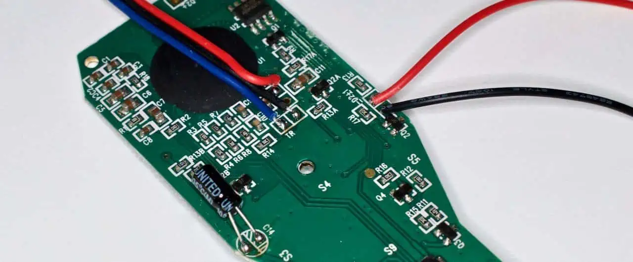
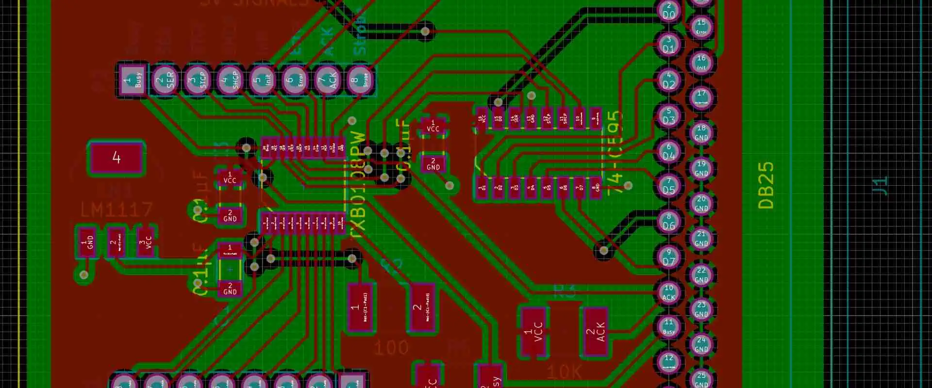
It simply defines the circuits’ reference node on the PCBs and is among the most used designation. A ground plane or sheet typically use to physically implement it. So the PCB design may have a quite low impedance returning the route to the source of power. This is crucial because if it’s not done, different “grounds” over the PCB can have different potentials. And the PCB might fail or just stop working altogether.

ยท Analog And Digital Grounds

As the states of the digital signals fluctuate, current spikes are in digital circuits. Current peaks are once more produced in the analog circuits when the current load fluctuates.

Even though there are several methods for doing correct grounding, it is crucial to distinguish between the “noisier” digital returning currents and the “lesser-noisy” analog returning currents whenever it relates to mixed-signal earthing. The generation of noise inside circuits owing to ground current flow is preventable by this isolation of the grounding.

When these ground currentsโ€”which you might conceive of as shifting currentsโ€”are directed to ground-returning pathways, noise is produced by voltage fluctuations (remember Ohm’s Law). You may be familiar with the phrase “a loud ground.” On local circuits, this noise might impair delicate signals. For system, test, and design engineers, grounding has long presented significant challenges.

A “star,” earth, or ground is one potential grounding method that may be useful in certain circumstances. This way of thinking is based on the idea that every voltage in a network refers to the same ground point.

On paper, the sole grounding location and star ground approach appear to be a brilliant idea. Based on how sophisticated one’s design is, it may be quite challenging to implement in practice. Using a ground bus bar is an alternate approach.

Nevertheless, remember that if a design employs a single common ground plane, return currents may be regulated by a good PCB layout. So there’s typically no need to physically separate the digital and analog grounds.

ยท Common GND In-Circuit Errors

For newcomers, a three-end DC energy source may seem somewhat confusing. There are three terminals on this power source: the positive (+) terminal, the negative (-) terminal, and the ground or GND terminal. The earth ground or ground terminal is physically attached to a chassis, which is then linked to the earth wire inside the power adapter. It is with Earth directly through the three-prong socket.

Beginners frequently make the error of connecting power between the GND and the positive (+) connections. No electricity will run since this improper connection prevents the current from going back to the electrical supply, which is where it gets its energy. Connecting the power between both the negative (-) and positive (+) terminals is the right connection.

ยท Electrostatic Discharge (ESD)

Your test device’s grounding also aids in the prevention of a discharge of electrostatic or ESD. Whenever a statically electrified body touches the test apparatus, ESD happens. Certain testing tools are extremely sensitive and can be quite susceptible to ESD incidents.

ESD shielding for the ICs is adequately provided by grounded mats. This also refers to ESD mats, wrist straps, and grounded chairs. This is because they ground you before you touch any sensitive electronic component, discharging whatever static charge you might have on the body. While working with Circuit boards and ICs, the majority of technicians and engineers also put on ESD-safe jackets as additional security against potentially harmful parts and equipment.

Common GND In-Circuit Problems

FULL PCB MANUFACTURING Quote

The voltage differential among “grounds” on several decks or areas of a yacht, for instance, might be in the volts of tens. When working on a ship deck, there are noticeable voltage differences between the ground on the electric extension cord and the person utilizing the long extension lead. Similar issues arise on airplane surfaces when they travel at extremely high speeds through the magnetic field of the Earth. As a result, there is a little voltage differential between the points of ground. 

 A voltage produces as the current runs through the substance. Impedance is present in conductors, wiring, junctions, as well as in soil.

While designing a circuit, it is best to keep all grounded nodes close to one another and steer clear of loops and numerous earth loops. Frequently, the power enters at this location, or the primary decoupling or smoothing capacitors with a chassis at this location.

High gains equipment, like amplifiers, will have a lot of current flowing via the ground wire. It becomes crucial to ensure that all these grounds aren’t with the amplifier’s input stages. If not, oscillation happens. Only at a single stellar ground should the output and input stages come together.

ยท Ground Loops

In high-output audio systems, connecting equipment with an independent mains power supply can cause ground loops. A mixing panel and a PA device, for instance, each with a separate main supply power source. Significant hum issues are there when the metallic grounding screen within the audio wires forms a loop with various mains earth.

When the demands on each stage are in a three-stage mains power system, the point of neutral should have zero potential. Rarely is this the case. Voltage variations, among other phases, will result from large current activity on one side, which will lead the neutral current to “float” higher. 

Do You Really Need GND In Circuit?

All circuits require a “ground” because every electrical system requires at least one return route to the power source. This “ground” is typically also useful as the referencing node for measuring all of the network voltages. Nevertheless, not every circuit connects to the line voltages (such as battery-powered electronics). Hence not every circuit will require earth “ground.” More accurately, a return channel via the earth. Similarly, a chassis returning route is not necessary for the safety of electronics in non-conductive environments. What we want is the ability to rename these roads to prevent misunderstanding with the ground.

Designing a Digital Thermometer PCB: A Comprehensive Tutorial

thermometer pcb

Unlike conventional thermostats, digital thermometers are unaffected by damage at extremely high temperatures. Thermocouples are frequently used by designers in industries to measure high temperatures. After you have the schematics of circuits for the Circuit layout of the digitalized thermometer, this post will assist you in understanding how to proceed.

Whatever components you utilize are entirely up to you. We would, nevertheless, provide you with some advice regarding some ideal electronic parts. You might be considering making your digital thermometer.

We’ll go through each step so you can successfully create a PCB digital thermometer.

YouTube video

1.ย Finalize Your Thermometer PCB Circuit Schematics

A digitalized thermometer may require for personal, professional, or industrial applications. You may require high-temperature resistance if you’re developing the schematics of PCB for industrial use. A microcontroller like the ATmega16 MCU may be used to measure temperatures up to 1024ยฐC.

For the digital thermometer to detect high temperatures, you might additionally need to utilize thermocouples. K-type thermocouples are the most popular kind. Given that it is dependable, accurate, and affordable, you are probably already utilizing it. Also, you ought to make use of ICs like the MAX6675 IC. It will digitally transform the K-type waveform and inherit cold-junction correction.

Since the device is cold and the thermocouple tip is not (0ยฐC/32ยฐF), cold-junction correction in electronic thermometers compensates for the absent thermoelectric voltage. You can get digital signals from the MAX6675 Integrated Circuits that are 0.25ยฐC precise. You may utilize seven-segment displays to obtain the display. Electronic thermometers can use with thermistors for household usage.

2. Make Layout of Thermometer PCB

Well, so you are ready to start constructing the digital thermometer PCB design once you complete the schematic of the circuit and create it in your preferred program. The PCB’s trace architecture and component arrangement are modeled by the schema.

Moreover, the PCB layout program will convert all traces, wires, and components into a format of PCB, speeding the process of designing.

It is essential to ensure that every schematic sign in an electronic thermometer corresponds to a PCB layout. The PCB layout specifies the physical size of the components as well as the location of copper pads or through-holes. You will next begin routing the cables for your custom-designed digital thermometer. Both manual and automatic routing options are available.

When all of the routings are finished, labeling the components or signs is a smart idea. The tags then transfer to the Circuit design and eventually appear on the finished PCB. Also, you may arrange electrical components across every area on the Circuit for the thermometer. It attests to the shortness of the conduction lines and traces. Long traces may amass significant quantities of electromagnetic waves, which can produce interference and noise.

3. Etch Your Thermometer PCB

A4 shiny or picture paper can use to print the PCB thermometer using a laser printer. To make sure the printout is on the article’s positive side, one must take a mirror image of it. Also, must choose the black output color in the printers and PCB design options.

Cut the copper sheet for the PCB thermometer after that. Depending on the PCB layout size, you can use a hacksaw or a cutter. To scrape the copper off the PCB, use steel wool or abrasive sponges. Any oxide or photoresist layer that may be on the Circuit board will be removed. The digital PCB thermometer printed design will then be transferred from the A4 glossy paper to the Circuit board.

Keep the printout and board in the proper alignment at this phase. To maintain these in the appropriate place, you can apply a piece of tape. The PCB design of the digital thermometer printout will then applies to a copper sheet using an iron. The reverse of the A4 Glossy paper will expose to the heated iron for between five and fifteen minutes. The glossy paper’s ink will transfer off the PCB by heat.

4. Drill Vias Into Thermometer PCB Sheet

Vias could have been employed while creating the PCB for the digital thermometer. The electronic impulse can travel along these routes as it passes through various circuit levels. If you’re new to PCB design or designing them at home, you can use through-hole vias. For drilling needs, you need to get in touch with a PCB maker if you’ve created hidden or blind holes.

Several vias cannot drill at home. For these objectives, PCB makers utilize particular automated drilling equipment. You’ll see that any PCB designing software can output a drill document. You must create the drill document, which includes all the specs for the holes needed for the finished PCB manufacture.

There’s no special method you may use if you want to drill. But, you must abide by the limitations on minimum diameter, maximum area ratio, and hole proximity. The maximum area ratio is obtained by dividing the thickness of the PCB by the tunnel width. Adjacency refers to the shortest distance that can allow between the edge of a hole and the nearest neighboring hole.

5. Solder the Electronic Components

Now, assembling the components of the thermometer PCB is a very straightforward process at this point. Resistors and Capacitors might also use as a starting point, then a battery connector and a thermistor, and finally ICs and screens. Always remember to install any DIL plugs on the PCB of the digital thermometer at the very end if you’re using any.

Be cautious while soldering of ICs if DIL plugs are not being used, though. Before securing the subsequent bolt, the pin must have cooled. They can harm small wires in the Integrated Circuits and are extremely heat-sensitive, thus the reason. Moreover, never leave the solder on an electric pin for longer than 4 sec. Before beginning to solder the remaining nails, wait a further five seconds. You can connect wires to switches and thermistors even if you’re not adept at soldering. The goal is to prevent soldering and put them on the chassis. You have the option of inserting the thermometer Board inside a plastic ring after soldering. The digital thermometer appears more polished as a result.

6. Test Your Final Thermometer PCB

Now that the PCB for the digital thermometer is complete, it’s time for a check for any assembly flaws. You may test the PCB’s functionality. On simulation, you may verify what LED lights up when the simulation is first started. To ensure the digital thermometer PCB is operating properly, you may add an indication LED to the circuit.

You may supply power to the PCB and see if the indication LED illuminates. To look for any open circuits or sparks, you may also insert the DMM’s probe between various circuit locations. These techniques are conventional. Thus beginners should avoid using them. PCB producers employ cutting-edge methods like beds of nails and in-circuit testers.

Contact RayPCB for Thermometer PCB

FULL PCB MANUFACTURING Quote

Don’t move if you feel that all of these processes are too lengthy and that you don’t have much time. We also offer the ideal choice for you. Just search for a knowledgeable PCB maker. They’ll need specialized equipment and tools to complete search all of these processes.

All you have to do is search online for PCB manufacturers, then submit a request on their site. You must submit documents like drill data and Gerber. The manufacturer uses these properly to create the PCB for the digital thermometer.

Conclusion

These are the seven procedures you need to know before starting to build the PCB for the electronic thermometers. You must create circuit diagrams using programs like Altium Design and Eagle. Then transform these into a Circuit board and print it out.

Use a heated iron to transfer the electronic thermometer printing on the copper plate. Then arrange the components, drill holes, and solder them. Test the finished PCB. Nevertheless, if you want PCB facilities, get in touch with us; we can offer the necessary technology, supplies, and services. Call or email us right away.

Avoiding Top 12 Common PCB Soldering Troubleshooting Mistakes

Soldering Circuit Boards

Making soldering errors is a common occurrence, especially when dealing with many PCBs. As a result, it is possible to encounter various soldering flaws while carrying out such tasks. Even experienced technicians can make mistakes, such as overheating or underheating a pad or applying too much and too much solder. To prevent these mistakes, it is essential to understand how to recognize defective solder joints.

YouTube video

Soldering Troubleshooting

Identifying soldering defects requires a trained eye. A correctly soldered joint should be clean, symmetrical, and have a concave shape compared to the neighboring joints. A defective solder connection will be disorganized and have a physical abnormality, like a swelled shape or a long stem. Here are the 12 Typical soldering mistakes and the resulting problems:

1. Disturbed Joint

One prevalent issue found in columns and rows of soldered connections is the disrupted joint. It is recognizable by its swollen, distorted, and occasionally flakey texture. The main reason for unsettled joints is any form of movement during the soldering process. For instance, if the board is positioned on an irregular surface and vibrates or tilts while the solder is applied, the joint can become disturbed or lose its integrity. Additionally, if the board experiences any movement or vibration while the solder is drying, it can also cause a disturbance in the joint.

Confusing Disrupted joints with cold solder connections is a common mistake. Although they have a Resembling appearance, the causes of these issues are different. In certain situations, reapplying heat to the joint & letting it solidify without any disturbance can fix the problem. 

In the coming days, ensure each joint is secure and stable when applying solder.

2. Cold Joint

A common issue observed on a freshly soldered circuit is the presence of icy solder joints. These joints are recognizable by their uneven and sometimes undefined appearance. These joints are typically the result of insufficiently melted solder during the application process. In addition to their unappealing appearance, cold connections are challenging. They do not provide adequate bonding and are prone to developing cracks over time.

Repairing an icy joint is possible by applying heat once again. It can be achieved by using a hot iron. Additionally, if there is an excess volume of solder on the joint, it can be removed by using the pointed end of the hot iron. To avoid cold joints from forming in the future, it is crucial to ensure that the iron is heated to the appropriate temperature before utilizing the solder.

3. Overheated Joint

SMT-Through-Hole-Soldering

One of the most noticeable blemishes that can occur on a set of newly soldered joints is the Burnt joint. This type of common forms when too much heat is applied during the soldering process. In contrast to cold joints, which result from Inadequate heat, overheated joints occur(happens) when the iron is excessively preheated before application. These joints have a burnt appearance with a lumpy and misshapen structure.

To rectify the issues caused by overheating during the soldering process, a burnt flux and its surrounding area can be scraped off using the tip of a PCB working tool. If necessary, a solution like an isopropyl alcohol can eliminate a burnt flux. The ideal way to utilize alcohol is by using a small toothbrush.

Overheated joints can be difficult to fix, making it important to avoid them at all expenses. To prevent this issue on typical days, it is crucial to ensure that the iron is heated to the appropriate temperature and to check twice that the connections are clear before starting the soldering process.

4. Insufficient Wetting of the Surface Mount

Failing to heat both the pin and the cushion during a soldering process can result in an inadequate surface mount, where the support elements do not flow on a solder cushion. This issue can be identified easily if irregularities are present across a mount’s row. If different props have correctly streamed on the surface while 1 or 2 extra mounts have retained their actual pin composition, it is likely due to an inadequately wetted place.

To correct an inadequately wetted pad during the mounting process, preheat the iron point to the required temperature and then implement it into a solder pad. Add more solder to the place, allowing it to flow and dissolve into the design with the pin’s solder. To prevent this recurring issue, heat the Pad earlier than heating a pin during future soldering applications.

5. Insufficient Wetting of the Pad

Insufficient wetting of the solder pad in the soldering procedure results in an uneven joint without bonding strength. Typically, in such cases, an ample amount of solder would have moistened the leads, but the pad absences the important bonding power. A common cause of this issue is applying solder to a soiled circuit board, where the dirty circuit board prevents proper bonding. Additionally, if the Pad & pin lack adequate heat during the application, the place may finish with insufficient wetting.

To fix the issue of an improper wetted pad, heat the iron tip to the appropriate temperature or keep it at the base of the joint. Allow the solder to flow onto the surface, ensuring it wets the surface properly. To restrain this issue from happening in the future, ensure that the board is clean before starting the application and preheat the Pad and pin to the required temperature level.

6. Insufficient Wetting of the Pin

If both the pad & pin exhibit poor wetting, it is likely due to insufficient heat treatment of the pin. It commonly occurs when the plug is not getting heat sufficiently, preventing the solder from flowing into place.

To address the problem of an incompletely wetted pin, heat the iron trading point to the required temperature and apply additional solder. It is important to touch the Pad and the hook with the iron tip during the reapplication process to condition these elements for the appropriate application. To avoid this problem in the coming days, ensure that the pin and the Pad are heated to the right level during soldering.

7. Solder Starved

A joint that has an insufficient amount of solder is a solder-starved joint. Such a joint lacks the strength to perform its intended function and can lead to board failure if not addressed. Even though an insufficient solder joint may exhibit good conductivity, the board would still not be safe to use until the issue is resolved by adding more solder to the affected joint.

To fix a solder-starved joint, heat the joint (connection) with the iron tip to the correct temperature and add solder to a spot as an original application. This process should make the joint stronger & reliable, similar to the other joints on the circuit board. Once completed, the joint should withstand stress & make the circuit safe for computer equipment.

8. Too Much Solder

An overabundance of solder presents another significant issue. These joints are easily identifiable on a circuit board as they appear round and bulging, resembling a bubble. In contrast, a properly formed joint with the correct solder amount will have a concave shape. Excess solder coverage can result in inadequate electrical conductivity, rendering the joint incapable of fulfilling its intended function. Although it may not be prone to stress fractures, it will not serve its purpose.

If you encounter an excessively soldered joint, the solution involves removing excess solder and reshaping the joint to achieve the desired concave shape. So to accomplish this, you can heat the endpoint of the soldering iron & carefully trim away the excess solder until the connection no longer appears inflated or round. The solder-sucker may prove helpful in removing the excess solder more easily.

9. Untrimmed Leads

FULL PCB MANUFACTURING Quote

The presence of untrimmed leads on joints is one of the most hazardous errors. These leads protrude like horns. They are easily identifiable with the naked eye. Unlike properly trimmed tips with a concave shape, these leads extend higher and may tilt slightly sideways. When two untrimmed charges make contact, a short board/circuit may occur. Additionally, even when the leads become upright, they can bend over time & make contact.

Correcting untrimmed leads is a straightforward process that involves cutting them to the proper size for the common joint. You can use the same equipment for solder cutting and bring a joint down to a similar height as others on the circuit board.

10. Solder Bridge

When an excessive quantity of solder liquefies between nearby joints on the circuit board, a solder bridge may form. The joints on PCBs are intentionally separate, and unintentionally creating a connection between two joints during soldering can render the board unusable. Therefore, it is crucial to rectify the issue immediately to avoid further problems.

These are the steps you can follow to separate the accidentally connected points by removing the additional solder:

Make your soldering iron hot and use its tip to cut the extra solder that connects the two points from underneath. It will create a canal. Widen the channel until the joints are at the proper distance from each other. After removing the extra solder, you can use the soldering iron to fix the connection shape if they look wrong. To avoid this issue recurring, it’s essential to use only the right value of solder during all applications, as excessive solder can melt sideways & collide with nearby joints.

11. Lifted Pad

In addition to joint-related issues, you may encounter instances where a solder cushion separates from the board. Overworking a joint or repeatedly applying heat to the solder can result in a lifted pad, generally due to excess stress on the board. For instance, when removing a solder short/bridging with the iron and scaling the lateral crosstalk away from a joint, you may accidentally lift much & dislodge the joint from aboard. The problem is more prevalent on boards with thin copper layers and no through-plating.

Repairing the lifted Pad can be a challenging task, but it is possible. The most useful method involves folding the solder and bonding it to the unbroken copper pathway. If there is a solder mask covering the trace, you will need to eradicate it to reveal a copper.

12.  Stray Solder

During the soldering process, it’s possible to end up with random bits of solder on the board due to messy oversights. These bits are not with the copper trace. They are with a flux residue. If these bits are not on the circuit board, it’s important to eradicate them before putting the circuit to use. If left unresolved, these solder bits can cause short circuitry in a PCB.

To eliminate solder from the PCB, you can use a sharp printed circuit board tool, like a small knife. Use the tool point to scrape off the solder bits from the board’s surface. It’s important to check the circuit twice to ensure that no extra solder parts are present before using it.

Conclusion

electronic assembly soldering

So, you have found this guide to be informative and helpful. If you find that you have made any of these common soldering flaws, do not discourage yourself. Becoming a specialist at soldering can take time & practice, and making mistakes is a normal part of the learning process.

While there is no guaranteed way to achieve perfect soldering, these tips may be helpful to follow:

Before soldering, inspect and become familiar with the printed circuit board.

  • Ensure that the joints & pads are clean and contaminants free and prepared for soldering.
  • Maintain the soldering iron in excellent condition, paying close attention to the tip.
  • Take the time and avoid rushing.
  • Practice frequently to improve your skills.

Evolution of Automotive Electronics Design

Automotive PCB Manufacturers

Auto electronics are electronics that manufacturers build to specifically operate in automobiles. Generally, technicians designing these electronics have to be extra careful and vigilant when designing and developing these electronics due to a couple of reasons. These reasons include that auto electronics tend to function in pretty harsh conditions or environments with extremely high temperatures. Therefore, inaccuracies in the design or development phases might lead to immense consequences. So how can you ensure that you find the perfect automotive electronics designer for designing electronic components for your vehicle? And if you are a manufacturer, how can you ensure that your automotive electronics are of high quality?

YouTube video

Automotive Electronics in a Nutshell

There are multiple manufacturers from across the world who manufacture high-grade automotive electronics. Moreover, the manufacturing process of automotive gadgets varies from one manufacturer to another and from one device to another. Generally, most electronic gadgets are produced using varying temperature grades, with various manufacturers defining their own temperature ratings. Due to these reasons, engineers and designers have to work hand in hand for them to meet the specifications of a customer.

Here is a list containing some temperatures grades or ratings that manufacturers utilize:

  • Military-grade: -550C โ€“ 1250C
  • Automotive grade: -400C โ€“ 1250C
  • Industrial: -400C โ€“ 1000C
  • Commercial 00C โ€“ 850C

You might be wondering, “why not just utilize the military-grade to generate all automotive applications?” The answer to this question is simply cost. Generally, the higher you go in terms of temperature ratings, the more costly the product’s manufacturing process will be. That is why the commercial electronicsโ€™ temperature rating stands at a range of 00C โ€“ 850C, reducing the cost of manufacturing these products and making them suitable for mass production.

On the other hand, aside from unique temperature ratings, gadgets that fall under the auto electronics category are the devices that manufacturers produce for them to function in an automobile. The design of these electronic products is such that they adapt to the harsh conditions of an automotive system. Electronic products that fall under this category include:

  • Infotainment systems
  • Telematics
  • Carputers

Carputers

 is the term that you get when you combine the words computer and cars. And just like the term indicates, a carputer combines cars and computers for optimal operation. Generally, manufacturers generate a customized personal computer, and then they integrate it into a car system. These customized personal computers tend to bring the following features to a vehicle:

  • GPS navigation
  • WIfi-capability
  • USB capability
  • Bluetooth capability
  • Music capability โ€“ specifically mp3
  • Video capabilities
  • Customized components
  • Low power requirements
  • Compact size

The first time manufacturers utilized a PC in a vehicle, it was utilized for optimal engine control. The computer used at the time was known as the ECU (engine control unit). Moreover, this first ECU was integrated into a Volkswagen back in 1968, and it had one sole purpose: to handle electronic fuel injection 0r EFI.

However, as of the 21st century, Volkswagen and other renowned car manufacturing companies utilize computers in cars to carry out multiple operations.

A Brief Walkthrough of how Early Car Manufacturing Companies were Integrating Computers in Cars

FULL PCB MANUFACTURING Quote

After the first computer system integration into a vehicle, various companies also began to follow suit in terms of adopting computers into their cars. Here is a brief overview of how this took place:

  • 1969 โ€“ The introduction of the very first PC-controlled anti-skid system in cars
  • 1971 โ€“ Introduction of the first comp-controlled transmission system by General motors
  • 1978 โ€“ introduction of a comp-controlled trip PC (which was working via a unique Motorola Microprocessor) by Cadillac
  • 1986 โ€“ Development of the very first self-driving vehicle (Navlab 1) by Carnegie Mellon University. Navlab 1 was completely autonomous, and it was a significant breakthrough for the automotive industry and the world at large.
  • 1986 โ€“ Development of the first multiplexing wire communication module with multiple chips by Harris Semiconductor
  • 1987 โ€“ Generation of the first auto microcontroller chipset, which was generated to CAN car bus standards by Phillips semiconductors and Intel
  • 2014 โ€“ Introduction of the first commercial self-driving car (Navia Shuttle)
  • 2015 โ€“ Introduction of the first semi-autonomous, self-driving semi-truck by Daimler’s

Telematics

Telematics is the term that you get when you combine the terms informatics and telecommunications. So in a sense, telematics is generally the integration of telecommunication using communication and informatics technologies. Or in simpler terms, this is the tech of storing, sending, and receiving information that relates to vehicles using telecommunication gadgets.

Here is a list that outlines examples of unique communications that use telematics or take advantage of it:

  • Road safety
  • Satellite navigation
  • Car sharing tech
  • Intelligent vehicle tech
  • Emergency warning systems meant for cars
  • Wireless car safety communication
  • Trailer/vehicle tracking

Infotainment

Infotainment is a term that combines two common words, entertainment, and information. Moreover, experts also refer to infotainment as ICE (in-car entertainment) or IVI (in-vehicle infotainment).

Generally, infotainment refers to a complex collection of various software and hardware components in a vehicle that offers video and audio content in a combo of entertainment and information. Most people argue that infotainment systems brought about the transformation of ordinary cars into smart vehicles. A smart vehicle is simply a vehicle that can offer impeccable entertainment facilities (for example, ear seat entertainment) while at the same time providing tech capable of various driver-assistance tasks, which include:

  • Assisting drivers during the parking process
  • Alerting drivers whenever they find congested routes and traffic jams and suggesting alternative paths that are better in terms of traffic.
  • Offering impeccable internet connectivity in an automobile

Generally, infotainment is among the major automotive industry trends fueling the integration of microelectronic systems in cars. As days go by, it is becoming pretty clear that most, if not all, drivers want always to be connected. Moreover, drivers want to access their personal content easily, anytime and anywhere, and this is only possible via automotive electronics.

As of the 21st century, automotive electronics are providing means to convert an ordinary vehicle into a “connected device effectively.” A connected vehicle is pretty efficient in terms of the following:

  • Comfort
  • Safety
  • Energy

Moreover, it also provides you with various benefits, such as having access to crucial information regarding road accidents, traffic jams, or the weather.

Specific and General Applications of Various Automotive Electronics

Automotive PCB Applications and Types

Today’s vehicles can have up to fifty computer systems that are dedicated to controlling and/or monitoring everything from onboard entertainment to ride handling and in-car communication systems.

Here are the specific and general applications of most automotive electronics that you can find in the market today:

Safety Applications

Automotive Radar Systems

You can easily find automotive radar systems in the market with varying bandwidths. These radar systems mostly have the following specifications:

  • Drivers utilize them for driver-assistance tasks such as blind spot detection and auto emergency braking
  • Short range implementation

Airbag Systems

Airbags are crucial systems in any automobile. Actually, as of the 21st century, having an airbag system in a car is mandatory in most countries. Most automotive electronics manufacturing companies provide flexible and scalable airbag systems that keep drivers and passengers safe.

Multi-purpose Camera Systems

Multi-purpose camera systems are efficient and compact camera systems integrated into automobiles to allow impeccable driver-assistance functions such as:

  • Pedestrian recognition
  • Traffic sign recognition
  • Forward collision warnings
  • Lane departure warning

With these automotive electronics in your vehicle you can overcome multiple obstacles that drivers face while on the road. Moreover, since their invention they have helped in terms of keeping road accidents low.

Tire Pressure (TP) Monitoring Systems

Tire Pressure (TP) Monitoring systems are crucial computer systems in automobiles that ensure accurate tire pressure. These systems are pretty vital since they offer the following benefits:

  • A boost in safety
  • Comfortable driving
  • A boost in handling

Powertrain Applications

Micro Hybrid

The micro-hybrid is a high-efficiency and start/stop generator. It is pretty useful in the following situations:

  • Electrical car launching
  • Car coasting/sailing
  • Engine brake emulation

Gasoline Direct Injection Systems

Gasoline direct injection car systems offer a boost in terms of measurement precision (misfire detection, ignition control). Moreover, it also helps in terms of efficient utilization of fuel, which saves you cash and also saves the environment from harmful carbon emissions.

Body Applications

LED Light Modules

LED light modules in automobile assist in terms of controlling the LED in vehicles. That means you can dim or diagnose all the LEDs in your car using these systems. Moreover, LED rear light modules tend to increase the lifespan of the car’s LED due to integrated protection.

Interior Light Controls (Touch Sensors)

Car systems now come with interior light controls, which you can manipulate using a capacitive touch sensor. The capacitive touch sensor replaces mechanical switches, ultimately saving you money. Moreover, these reliable and robust touch sensors instantly take your car to the next level.

How Automotive Electronic Designs have Evolved Overtime

Automotive PCB

The number complexity and functionality of various auto electronics in the 21st century have grown beyond bounds and leaps over the last couple of years. Obviously, the famous Tesla automobile is the flagship, or what people are now terming as the standard for smart cars. However, even if you can’t afford a Tesla, that doesn’t mean you can’t experience the luxury of a smart car. Currently, automotive manufacturers and Assemblers are utilizing this tech in the lower-end and mid-range vehicles that most people can afford. And all these is due to something known as the automotive electronics design evolution.

Tech Functionality

The world is now evolving into an era of self-driving autonomous vehicles. That means the number of electronic gadgets in cars is about to get even higher and more complex. But what does this mean to the designing process of automotive electronics?

However, as we await these vehicles to take over the automotive industry, we can enjoy the complexity and efficiency that comes with present-day smart cars. Even though this technology is efficient, it doesn’t come without some issues in terms of the requirements of the product manufacturing part. Generally, automotive electronics come with some specific characteristics.

The characteristics include:

  • Printed circuit boards tend to range from single-layer flexible printed circuit boards to 12-layer printed circuit boards.
  • The skill sets of various designers tend to range from high currents (if they are working with generators, motors, and batteries) to radar systems.
  • Automobiles contain a lot of electronics. Actually, the spectrum that automotive electronics cover in the field of electronics is so broad that you can find any electronic product that you can think of under this category. Moreover, the spectrum that automotive electronics covers is so broad such that it rivals that of airplanes.
  • Automotive electronics provide vehicles with autopilot features that let the car drive autonomously without the help of the driver.
  • Automobile electronics must function across a pretty broad frequency spectrum which can range from 70GHz radar to stereo and everything that lies in between, for example, Wireless Ethernet, Bluetooth, and GPS. For example, Tesla’s tends to communicate with various cell towers as the driver is on the move. Moreover, these vehicles use embedded computer systems to report crucial data to the car’s manufacturer. For example, it might send a report containing its current location and its current status in terms of performance.
  • With modern vehicles, there must be a high-bandwidth network
  • These electronic gadgets are cost-driven. Therefore quality comes at a cost.
  • When it comes to automotive electronic designs, reliability tends to go hand in hand with cost. Therefore, even if you are looking to cut costs, ensure you do not compromise on the quality of electronic gadgets that you utilize on your automobile.
  • The signal integrity of automotive gadgets tends to match that of high-functioning, complex electronic products. Therefore, when you are generating an automotive electronic design, you have to keep this in mind.

Uniqueness of the Automotive Environment

Generally, automotive electronics are unique due to a couple of reasons which include:

  • Automotive electronics must have the ability to function impeccably under a temperature range of -600C to 1300C. Moreover, these components have to be able to tolerate this harsh environment for over 20 years.
  • Moreover, automotive electronics must have the ability to effectively tolerate intense vibrations and shock for an extended period.

Communication is Key

Generally, every product that you can find within a vehicle is interconnected, and it requires some type of communication technology to work seamlessly. The first automotive electronic designs were incorporating controller areas network buses. These buses enable multiple microcontrollers and varying types of gadgets to communicate effectively in real-time. Moreover, CAN buses did not need a host computer to run. With CAN, whenever you integrate a new gadget into the system, it effectively scans each and every component on the controller area network. Then it finds a way to work seamlessly with the system.

A CAN network tends to operate at varying speeds as follows:

  • Class A โ€“ 10 kbps
  • The Class B โ€“ 125 kbps
  • Class C โ€“ 1 Mbps

Moreover, above all these functions, a CAN could also keep your car’s interlocking brakes functional. However, most automotive electronic designers are now replacing CAN buses with Ethernet networks which are more efficient and reliable.

Ethernet networks can access data faster compared to CAN buses. Moreover, these networks have the ability to offer bandwidths that are necessary for high-demand automotive electronics, for example, various cameras that come with modern-day vehicles.

Tech Variations

The complexity and amount of tech in various cars can range from sophisticated to common depending on multiple factors, which include:

  • The carโ€™s model
  • The car make

It’s not been long since the official launch of GPS navigation systems in automobiles. However, when they hit the market, they were only available in expensive car models and makes. Moreover, the cost of these systems was also pretty high; hence most people could not afford them. However, as of the 21st century, GPS has become ubiquitous, which means that it comes pre-installed in most if not all, smartphones. Moreover, it might be challenging to now find vehicles that come without GPS functionality pre-installed. Furthermore, the price of adding this system to a car has decreased immensely, which means you can now have GPS even if your car did not come with it.

However, as seen earlier, if you are willing to spend more, then you are likely to get more in terms of automotive electronic designs. That is because high-end cars tend to come with more sophisticated gadgets. Moreover, with every single model that they release, they add in new tech, which makes this vehicle pretty efficient.

Designing Reliable Automotive Electronics for Various Electronic Cars

Automotive PCB

If you would ask a few of your friends this simple question, “What makes this world revolve?” they would probably give you varying answers. Some might tell you that it is love, others might say it is information, while others might say it revolves due to energy. However, once you remove all the abstract, the answer to this question is energy.

In the era that we are living in, energy drives almost every single thing that you can see or touch. Moreover, you can further refine this to find that electrical energy, or what most people call power, is the most commonly utilized form of energy. However, the ability to effectively distribute sufficient electrical energy to various systems in a reliable manner has become a significant challenge to most people.

EVs or electric vehicles and HEVs or hybrid electrical vehicles face this challenge too. However, when it comes to vehicles, you can view this issue from two distinct perspectives:

  • Availability of charging stations
  • Distribution of electrical energy to the vehicleโ€™s electronic system.

Designers and engineers of auto electronics systems, devices, and PCBs tend to assume the former while taking the latter as a crucial design concern. For instance, material selections tend to depend on electrical energy distribution across the board. Therefore, let us look at electric car systems and how designers can generate automotive electronic designs for these vehicles to optimize electrical energy distribution.

Automobile Electronics for Various EVs

Generally, traditional EVs use a 12V direct current energy supply system. However, HEVs and EVs have evolved over time, and this energy supply system has become inadequate for modern-day EVs and HEVs. As a result, Modern-day HEVs now rely on a 48V direct current energy supply. On the other hand, EVs rely on a 400V direct current energy system. What this means is that the battery of the vehicle is 400V or 48V, even though individual electronic might operate under lower voltage levels. However, putting aside the fact that EVs need high electronic energy to function, there are a lot of advantages that come with using a current supply system in these vehicles.

The effective transmission of direct current electrical energy over various conductors comes with pretty high losses as different gadgets dissipate heat to the environment. However, this is a great concern for Cu (copper) because of its high HTR (heat transfer rate). Moreover, high voltages come in handy when it comes to supplying high-power components and gadgets.

To effectively supply electrical energy to every automotive electrical and electronic system, EVs use staged power conversion. The stages power conversion process encompasses DC-AC inversion or conversion and DC-DC conversion.

Similar to ordinary (non-electric) EVs contain multiple systems and components that undertake various operations. These components and systems include:

  • Accessory control
  • Major functions
  • Monitoring
  • Lighting

Generally, standard vehicles include approximately thirty thousand electronic components. Moreover, HEVs contain around the same amount of components since most vehicles need around the same amount of components to carry out electric and combustion operations.

Conclusion

The automotive electronics industry has grown over time. However, this growth means that automotive electronics designs have also evolved. For example, we have moved from traditional CAN buses in ordinary vehicles to Ethernet systems in modern-day cars. Moreover, EVs and HEVs have also evolved in terms of power intake due to the integration of computer systems. However, this evolution means vehicles are becoming more powerful and efficient.

What are the Various High Speed Cable Assemblies?

High Speed Cable Assemblies

Applications that need high speed contacts to ensure data and electricity transfer could benefit from different high speed cable assemblies. Such cables are made to offer applications better electrical performance. They comprise of shielding manufactured from quality material, which can practically eliminate any sort of external influence.

Fiber optics are among the most typical applications for high speed cable assemblies. They are suitable for a number of applications, which include military, avionics, data storage, and telecommunications. Also, they can be utilized for I/O, tiny pitch, as well as space-saving needs.

High speed cable assemblies may offer a wide range of employment opportunities. A wide range of companies across all industries that need to use electronic hardware require cable assemblies.

High speed cable assemblies can be used in a variety of outdoor and indoor situations because they’re designed to store and arrange a large number of different electrical wires safely. The people installing cable assemblies usually keep their cables and wires incredibly orderly, which is much appreciated. This makes it possible for them and upcoming electrical workers to access electrical systems safely and conveniently.

YouTube video

Features of the High Speed Cable Assemblies

There are a few fundamental things to keep in mind when buying high speed cable assemblies.

Design: The cables often are produced in the flat ribbon shape. This design enables multiple folds as well as a small bend radius. This same Flat Ribbon structure reduces the size of the cables, which frees up space in applications that are cramped.

Pitch: Several pitches may be employed to construct one high-speed cable. This happens because one cable could be connected to many connections for usage in applications. Cables having pitches 0.50 mm and 2.54mm make up high speed cable assemblies.

Male and female connections are both available for high speed wires. These cables can be installed with power and signal connections, in addition to metric power sockets and headers.

Power and Signal: To ensure there isn’t a lot of electrical power or data loss, the cables are built with substantial shielding. Its transmission efficiency increases with stronger shielding. The barrier prevents noise from leaving power applications.

The cables shield signal applications from noise, ensuring optimal performance. Due to these characteristics, high speed cables are very helpful for delicate applications.

Ways in Which High Speed Cable Assemblies Assist Applications

High-speed delivery could be ensured by cables without producing any form of congestion. High densities are used in the manufacturing of the cables without compromising efficiency. This enables them to offer great high speed application performance. Also, these  cables do away with the requirement to use many cables for a single application.

In commercial and industrial settings, high speed cable assemblies could deliver unmatched performance. Also, they are made to be valuable in terms of reducing space, having lower expenses, as well as having excellent value. Applications that need high speed connection for the transport of data and electricity can benefit from high speed cable assemblies in a variety of ways.

Such cables are made to offer applications better electrical performance. They are made up of sturdy material shielding that can essentially block all outside disturbance.

Fiber optics is among the most typical applications for high speed cable assemblies. They have a wide range of uses, including data storage, military, aviation, and telecommunications. Also, they can be utilized for I/O, tiny pitch, as well as space-saving needs.

The proper functioning of systems which process enormous amounts of data depends on high-speed wire assemblies.

High Speed Cable Assemblies Applications

FULL PCB MANUFACTURING Quote

Applications for High Speed Cable Assemblies are numerous. They include, for instance, flat panel screens. Throughout the 1990s, the flat panel display panels have grown extremely popular for different commercial, consumer, as well as industrial purposes.

Whether it’s the television sold in the store or the display screen inside the cockpit of an airplane, cable assemblies serve as a crucial component of every flat panel displays.

Systems for in-flight entertainment

Commercial airplanes use cable assemblies for making sure that TV screens installed in each passenger seat’s headrest operates properly.

Navigational systems

Cable assemblies assist the operation of vehicle navigation systems inside a variety of vehicles, including police cruisers, fire trucks, taxis, as well as private automobiles.

Flight simulators

Pilots in the armed forces, the commercial aviation industry, and private aviation can all benefit from the highest flight training level thanks to cables assemblies which fulfill the performance targets and close spacing specifications of modern flight simulators.

Commercial and military ruggedized PCs

Cable assemblies serve as essential parts in shock-resistant and ruggedized electronic applications.

What Benefits Do High Speed Cable Assemblies Offer?

End-use applications can now function to higher requirements thanks to cable assembly. Cable assemblies have the ability to provide both customers and manufacturers a number of advantages.

Safety

For the secure consolidation of possibly harmful electrical wiring, high speed cable assemblies remain essential. These enable electricians to ensure the wiring is kept tidy and shield it from the elements at the same time.

Service Period

Cables are shielded from damaging environmental influences and are prevented from being twisted or deformed by wire harnesses. The wires’ overall life is improved as a result.

Space

The high speed cable assemblies assist manufacturers in making the best use of available space inside electronics to make place for extra components and parts. Wire harnesses reduce clutter caused as a result of each loose cable, even if extra space is not needed.

Customizable

Bespoke cable assemblies frequently support a particular product capability. As contrast to off-the-shelf items, the cable assembly manufacturer that offers fully customized solutions could give a higher availability level for exact design specifications.

Cost and Time

Every firm needs time on a demanding production day. Because of this construction, every one of these wires which are ordinarily strewn about, difficult for the technicians to distinguish between, and loose are bound together. This eliminates the necessity of the time-consuming installation process and increases the amount of time available for research, should a problem arise.

Organization

Instead of being dispersed and twisted, cable assemblies were kept in one place. This is crucial for heavy-duty applications like aerospace and defense because it makes it simpler to move the various parts and reduces the possibility of damaging those cables and having to pay for pricey repairs. Also, it indicates that worker security is not in danger.

High-Speed Cable Assemblies Examples

Fiber optical cable

The network cable with glass fiber strands inside of the insulated housing is known as the fiber optic cables. They are made for telecommunications, long-distance, as well as high-performance data networking. Most cable televisions, internet, as well as phone systems in use today are supported by fiber optic connections.

At least one strand of glass, with each barely thicker compared to human hair, make up the fiber optic cables. This core, which offers the path allowing light to pass, serves as the core of every strand. In order to prevent signal loss as well as allow light to travel through bends inside the cable, this core is encased in a glass layer known as cladding.

Coaxial Cable Assemblies

For valid reason, the assembled coaxial coaxial, round, or simply “coax” cable has not been a recent development. These small workhorses consistently deliver excellent performance. You probably don’t have to search very far to see one being used; it’s typically a round, white or black cable with the distinctive metal “F-type” connection, which has a pin placed inside the middle, that connects to your Television. Bundles of coaxial cable with a variety of terminations, couplings, etc. are used to create the coaxial cable assembly.

Here, makers of custom cable assemblies have a big advantage over those of generic cable and off-the-shelf assemblies.

Military Cable Assemblies

Military applications were renowned for being exceedingly tough. For the cable assembly intended to be utilized in military contexts, rough terrain, challenging environmental conditions, RFI/EMI, as well as the greatest utilization rates are likely to be encountered. To perform a close-range bomber operation in the supersonic fighter plane or to enable troops to connect with their superiors, who are frequently thousands of miles away, our combatants depend on the cable assemblies such as the ones that we are proud for manufacturing.

Military cable assemblies frequently need to be designed with sufficient flexural strength to countless cycles. Flexural capability is essential to maintaining the electronic system’s best performance during fast runs for extended periods of time.

Assemblies of RFI/EMI Shielded Cables

Like or not, each and everyone of your cords is contributing to the incredibly loud electrical environment in which we live. Undoubtedly, electromagnetic interference and RFI can have an impact on wires. The device’s electrical system experiences multiple interruptions as a result of such interferences.

For instance, you can encounter data loss, bad signal quality, decreased performance, and sometimes a full cessation of the device’s activities. So, choosing a RF/EMI shielding to serve the cable assemblies has been the ideal method to get rid of this.

There are two primary kinds of shielding options: braided and foil shielding. One goal of foil shielding is to completely enclose each conductor inside a cable arrangement. Contrarily, braided shielding encloses the whole conductor by weaving copper in a mesh. Similarly, braided shielding provides more immunity to interferences yet is more expensive. Contact the interconnection solutions for determining which shielding solution is suitable for the device as well as the environment.

Wire Harness vs. Cable Assembly

Cable assembly

The cable assemblies serve as collections of wires and cables which are held together by an outer covering of different material. Cable assemblies’ main purpose is to maintain the the cables and wires orderly. Typically, wire harnesses and cable assemblies perform comparable tasks, but they are made for quite distinct situations.

They are typically constructed of robust materials including thermoplastic rubber, vinyl, and shrink-wrapped thermoplastics.

Wire Harness

The tiny cables and wires within are covered by wire harnesses, which are more like a simple outer coating. Wire harnesses are used to combine wires and cables that are already covered by an exterior layer of protection. This basically means that instead of just one wire, one would see many cables that have their individual covers if you opened a wire harness. Thermoset and thermoplastic materials have been used to make wire harnesses to suit a long time. These materials would aid in shielding the cables from the elements.

The cheapest electrical approach for organizing your electrical systems cleanly is wire harnesses.

Related Questions

Why does UL certification play a crucial role for wire harnesses and cable assemblies?

United States government has granted Underwriters Laboratories permission to test products and processes for safety, usability, and compliance with design standards. UL serves as the independent testing agency.

We are pleased to use UL-certified wires and cables in all wire harnesses and cable assemblies because we are a UL-approved manufacturing facility. Our engineers can employ professional solutions without the need to create new ones if we have a wire or cable with defined parameters and viability.

How could high speed wire assemblies maintain product safety even under the most difficult conditions?

Cable assemblies comprise collections of cables and wires which are wrapped in a very robust material, such as vinyl or shrink-wrapped thermoplastic. In terms of size requirements and their capacity to protect their internal cables against hazards such as water, extremely high or low temperatures, friction, as well as oxidation, the cable assemblies have been suited to such environment.

Punishing applications, like the ones that our military personnel encounter, frequently involve a few of the harshest situations on earth and have extremely high utilization rates. Whenever you are working inside a small space, the combination of durability and strength poses a significant design challenge, but our professional engineers like finding solutions to challenging issues.

To begin the cable assembly designs for your project, gets in touch with our professional sales staff right now.

Conclusion

In summary, high speed cable assemblies can be used in a variety of outdoor and indoor situations because they’re designed to store and arrange a large number of different electrical wires safely.

What are the Methods for Interconnect PCB?

hdi pcb design

Electrical contacts are present on both electromechanical and electronic components, and interconnection is the term used to describe this same electrical connection in-between both discrete contacts. To perform the desired function, electronic equipment must be connected in line with the schematic of the circuit.

A PCB cannot typically be considered as electronic product because it is a component of the entire machine, thus it needs to have an issue with the external connection. Circuit boards, as well as off-board components, PCBs, as well as equipment panels all need to be connected electrically. Among the key components of circuit board design is choosing the optimal combination of dependability, economy, and process. There are numerous ways to link externally, so you’ll have to make flexible decisions based on various factors.

Factors to Consider During Interconnect PCB Design

Although it is possible that the multi-board solution is not the best strategy as regards functionality, there really are circumstances in which you must employ this strategy.

It might be as straightforward as allowing for a specific form factor and the requirement to quickly segregate power or delicate signals. You can be accused of employing custom boards or a “off-the-shelf” circuit board to communicate with particular components (like LCD displays).

Creating for the future expansion (such as the usual Arduino shields), establishing several design configurations (perhaps the basic version as well as the advanced version), and simply making the design modular generally are additional reasons for the stacking of boards.

The finished interconnect PCB, and application would reflect the same degree of the quality preparation provided you adhere to a decent strategy and use sound principles to prevent frequent errors and dangers.

Complex projects require collaboration with a PCB assembly and manufacturing provider having engineers who have collaborated with as well as modified several layouts in advance of the assembly and fabrication of the electronic interconnects.

How do Interconnect PCB Get Processed?

YouTube video

The connector clip interconnection technique is frequently employed in increasingly sophisticated equipment and instruments. The structure of the “building block” not only guarantees the mass production’s quality, but also lowers the system’s cost and makes system debugging as well as maintenance easier.

Whenever a device malfunctions, maintenance staff do not need to go down to a component level; such that, they can only check the individual component for the failure’s cause. ), so far maintenance employees determine which PCB is aberrant, they can instantly replace this PCB, that not only eliminates defects in the quickest amount of time, but also reduces downtime. As a result, it can increase the device’s use rate. This replaced PCB may also be fixed over a long time and subsequently utilized as different spare parts.

In more sophisticated equipment and gadgets, this connectivity is frequently used. This approach creates its printed plug out from Circuit board edge, then the plug component is tailored to meet the specific PCB socket by taking into account the socket’s size, the connectivity points, the distance of the contact, its positioning holes, as well as other factors.

This plug section of a PCB requires being gold-plated in order to increase wear resistance as well as decrease contact resistance. This part works well for mass production because of its simple assembly, wide interchangeability, plus good maintenance performance.

This method’s drawbacks include higher PCB costs and stricter criteria for procedure and quality during PCB fabrication. Its dependability is also subpar. For instance, it frequently results in poor contact since the plug area is oxidized and the socket spring ages.

This very same outgoing lines is frequently carried out in the parallel form through contacts onto the same or the two sides of the PCB to increase the external interconnection’s reliability.

What Benefits do Interconnect PCB provide?

While prototyping, there are several different PCB types to pick from, ranging from straightforward one-sided Circuit boards to very intricate multi-layer boards. Copper tracks, and linkages between components, are often found on just one of the surfaces of the simplest prototype PCBs. Such boards are referred to as single-sided PCBs or one-layer PCBs.

These circuit boards are quite small. Engineers seeking more wiring capacity may choose HDI PCBs as one of their top choices for the engineers searching for the least circuit board having the highest output.

For those seeking smaller boards devoid sacrificing quality, HDI capacity simplifies the process to convert a 10-layered Circuit board into a four- or five-layered one. It may represent a significant design advantage because the majority of consumers favor compact devices.

the capacity to fit more components solely on a single side. The HDI PCBs use buried and blind vias, as well as Via-in-Pad technology, to cram components closer together for quicker signal transmission. It is therefore the best technology for the RF circuits.

Boards are transformed into sophisticated electrical circuits using the laser drill technologies. This manufacturing method enables the use of smaller holes thus increases the board’s heat resistance.

Fundamental Design Principles for Resilient Interconnectivity

FULL PCB MANUFACTURING Quote

Having the proper entire product goals, consumer/market insight, as well as target standards is the first step in creating a solid PCB plan. We can start designing the pcb as well as other necessary components after this point.

This is normally done in your favourite PCB design program. There are various tools at your disposal, yet you ought to use one which excels at fusing PCBA designs as well as using the 3D visualization to supporting PCB stacking, like Cadence or Altium Designer’s Circuit design tools.

Simplify your perspective in the design program to show split planes as well as return paths in between boards. If such digital signal should indeed bridge a break in power reference planes, close the troublesome signal using 1 or 2 decoupling capacitors.

Another general rule is to steer clear of broadside and parallel routing because these configurations result in more PCB crosstalk compared to perpendicular routing. Whenever stacked on top of one another, traces absorb more radiation because they are wider compared to being thick.

That overall connection between the traces is reduced by making them perpendicular.

Considerations for Board Stacking

Stacking boards on the top of one another with connectors dividing the boards is a frequent method of connecting several boards. The substrate must be carefully considered when designing boards that will be stacked in order to reduce the discontinuities in impedance, too much electromagnet emissions, as well as signal coupling.

Every signal layers ought to be near to and contiguous to a continuous reference plane. Strongly tied planes significantly lower electromagnetic radiation as well as lower top-end AC impedance. By directing high-speed signals in-between the planes, radiation is even further diminished.

Why It’s Important to Define the Appropriate Components

While looking for the different parts you’ll need to put the circuit board together according to the design, then you have a few options. Undoubtedly, the internet is a goldmine of knowledge, but sifting via the marketing speak may be overwhelming.

Speaking with representatives from manufacturers may prove to be a fantastic means of learning about new products, but once more, you are dealing with a salesperson that, eventually is attempting to sell you a product.

Yet, a manufacturer who is prepared to share knowledge and give you access to samples, past experiences, and industry norms can be a fantastic resource.

PCB Interconnection Method Procedure

Second-order HDI PCB Design

Method 1: Welding

This connection method does have the benefits of low cost, simplicity, high reliability, as well as the capacity to prevent failure due to inadequate contact; nevertheless, the maintenance and interchange are difficult. This approach is typically suitable when the component contains considerably fewer leads.

Welding of the PCB Wires

So far these wires are utilized in directly soldering the external points of connection on the circuit board towards the components as well as other components on the outer part of the board, the technique doesn’t need any connections. For instance, a radio’s speaker, the case of a battery, as well as the like.

During soldering, pay attention to how the board is connected:

  • To make maintenance and soldering easier, the soldered wires pads should be placed as near the outermost portion of the PCB as possible.
  • The hole must be drilled close to a solder joint present on the PCB board to ensure that the wearing of the wire is done from the printed board’s soldering surface. This will increase the wire connection’s mechanical strength and prevent the wire and these printed wires from becoming pulled off as a result of the pulling of the wire. Insert this pad hole out from the surface of the component for soldering through its via hole.
  • Organize or bundle these wires properly and secure them to the plate with wire cards as well as other fasteners in order to keep them from breaking owing to movement.

Welding of PCB Cables

These two PCB boards are joined by any cable that is both reliable as well as difficult to interconnect, and their relative locations really aren’t limited.

The direct soldering present between these printed boards is a common method for making a 90-degree angle formed between both printed boards. When linked, it transforms into a single printed circuit board components.

Method 2 of PCB Interconnection: Connector Connectivity

This connector connection technique is often employed in more complex equipment and instruments. The structure of the “building block” not just ensures product quality in mass manufacturing, but it also lowers system costs and makes troubleshooting and maintenance easier.

Whenever the equipment fails, their maintenance staff are not required to inspect the level of the component (that is, to investigate the reason for the failure and trace it back to specific components). The above work takes significant time), yet once  abnormal board has been determined, it may be immediately replaced, allowing for the quickest troubleshooting, reducing downtime, as well as increasing the utilization of the equipment.  

This replaced circuit boards could be repaired within a reasonable period of time before being utilized as spare parts.

Socket for Printed Circuit Boards

This connector is frequently utilized in more complicated instruments. Within that manner, each printed plug has been formed from the PCB edge, and its plug part gets designed to meet the unique PCB socket based on the socket’s size, contacts, as well as the distance between contacts, the location of a positioning hole, and so on.

The plug component of the board must be gold-plated during manufacture to improve the wear resistance as well as decrease the contact resistance. The approach is easy to build, is interchangeable, and provides high maintenance performance, making it ideal for a standardized mass manufacturing.

The drawback is that printed circuit board’s production cost is reduced, but the precision of manufacturing as well as process requirements are increased; the reliability comes slightly lower, and its contact is frequently weak owing to the oxidation of its plug section or aging of the socket spring. To help improve the external connection’s reliability, this lead wire comes frequently routed in parallel across contacts on both or same sides of circuit board.

This PCB board socket method of connection is frequently utilized for products of multiboard structure, as well as the socket, printed board, as well as bottom plate contain two main types of pin and reed.

Pin Connection (Standard)

This technique is helpful for connecting this printed board to the outside world, especially in compact instruments. Both printed boards were linked by the standard pins that are normally either perpendicular or parallel, allowing for easy mass manufacture.

Conclusion

A PCB, as a component of the entire machine, cannot in general create electronic products, so there has to be an issue with external connectivity. Electrical connections, for example, are needed between PCBs, components and PCBs, PCBs as well as device panels, and so on. As a result, among the most significant topics in Circuit board is the selection of the optimal connectivity that combines reliability, economy, and manufacturability in one. There are various types of connectivity methods from which we can choose based on the various properties of distinct interconnections.

How to Achieve a Successful Modular PCB Design

Modular PCB Design

Printed circuit board design can involve the connection of modules having different functionality. You can create simple designs without the impact of a PCB layout on the PCB operation. Also, a simple design might not require you to consider the relationship between several functional blocks on your circuit board.

However, more complex PCB designs require you to consider a lot of factors. You will need to not only consider the overview of your board, but also consider other parameters. The modular PCB design is implicitly integrated when designing circuit boards for various applications. This design methodology is beneficial to embedded systems, mixed signal systems, and multi-board systems. Other circuit boards with high functionality can as well benefit from this design.

YouTube video

What is a Modular PCB?

A modular PCB is a piece of hardware that features a particular functionality. This circuit can be connected as part of other circuits. A modular PCB is a circuit separated into modules rather than one complete setup. This refers to splitting a complete printed circuit boards into several circuit. Connectors or via cables are used in connecting these several circuits to each other.

The modular PCB design  is not a new concept in electronics design.  A good example is the assembly of computers. A modular PCB for computer comprises  single motherboard having slots for sound cards and graphics cards. Platforms such as BeagleBoard and Arduino highlight the modular design trend ans as such it enables the connection of independent modules in an ecosystem.

Furthermore, modular PCB design provides better flexibility for designers to perform some tasks.

What is a Modular PCB Design?

Modular Electronics of Raspberry Pi

The modular PCB design is integrated when designing circuit boards for various applications. This design methodology is beneficial to embedded systems, mixed signal systems, and multi-board systems. Other circuit boards with high functionality can as well benefit from this design.

You will realize some design tools canโ€™t be used due to inconsistent data formats and lack of unification. However, some design software are upgrading their tools to meet the demands of modular PCB design. Also, PCB designers can have full access to these design software packages. There are some unified PCB design software packages that feature set of tools for modular PCB design.

In those days, PCB design involved treating each part of an electronic system separately. The design process barely considered the connections between various parts of the systems except when complex boards are being created.

However, the electronics industry is constantly evolving as electronics are becoming connected and smarter. Consumers now demand improved functionality. Therefore, PCB designers are seeking for ways to embed this functionally in a device.

Modular PCB design is one such approach designers are now integrating. This design methodology takes an electronic systemโ€™s hierarchical view. Also, it is a multi-board design methodology which enables the separation of functionality on various boards.

Modular PCB Design Process

When we talk about a modular design, you might need to view your device as regards separate functionality. The easiest way is starting with your deviceโ€™s functional block diagram. Designers will need to understand how different parts of their device work to offer the functionality they need. Also, desired outputs and inputs will need to be considered in this case.

Furthermore, you will have to consider the functional block diagram as part of your design process when a device comprises central processing. Therefore, it is crucial to make some changes to the design when you begin the PCB layout process. The majority of PCB designers donโ€™t consider the interaction between functional blocks in their device before they start laying out their circuit board.

Designers may have to develop better block diagrams that reveal the functionality of each part of the device. This means that a hierarchical approach is needed in designing the key features of the board.

How to Use Schematics for a Modular PCB Design

The first step in a modular PCB design is to create schematics. As regards modular design, you can create connections between PCB components within every functional block in the diagram. With this, you can begin the modular PCB design.

The hierarchical schematic editor can help in connecting schematics. This tool is designed for PCB design. Therefore, this enables you to define the interactions between several schematics. Also, this can help you remain organized all through the design process and enable you focus in one part of the design.

Furthermore, you can connect several schematics within higher level parent schematic. In several systems, you will reintegrate some parts of your PCB design. In such a case, you donโ€™t need to redesign parts of your boards in various schematics. Modular PCB design enables you to reintegrate parts of your design in various schematics. Therefore, you donโ€™t need to rearrange the same components several times.

You can transition the board layout stage once the relationships between schematics have been defined and the functional block diagram has been transformed in hierarchical schematics. Furthermore, it is necessary to capture the schematics on a new board. You can now begin the process of arranging the components once the connections and components have been captured.

The Layout Phase of Modular PCB Design

FULL PCB MANUFACTURING Quote

After importing the schematics as the layout, you can now arrange components on the board. Using the appropriate schematic capture tool will help in ensuring your organization remains defined in the schematic. Also, it will reveal the connections between components. Some circuit boards will have their functionalities divided into various parts of the board. For instance, you should design the mixed-signal systems in such a way that the analog and digital areas create functional blocks.

In such a case, every block will need separation in its areas. This will help ensure signal integrity. After you add more functionality like wireless communication or Wi-Fi module, the layout should be in its functional block. The designer will need to assign every type of functionality to their area of circuit board in to ensure signal integrity.

Modular PCB Design Software

Modular PCB design is a process that requires some additional tasks. Therefore, the software integrated for this design needs to feature some functions other design packages donโ€™t offer. The modular PCB design software must feature multi-channel schematic editing tools. PCB designers will be more productive when the software also features a schematic editor and a schematic capture tool.

Another crucial feature a modular PCB design software should have is component management. Designers will have to reuse several components in various locations all through the entire board when carrying out multichannel design. This means a component library that comprises your design features will be needed.

The ability to integrate these features in only one interface enables easy generation of layouts and start component arrangement all through the system. Also, the layout editor will enable the grouping of components, which makes component rearrangement easy. With this, you can correct any layout errors and stay organized before you commence with manufacturing.

Efficient PCB design software will offer you a working environment that enables you have access to sophisticated tools. There are some features that enable you achieve an excellent modular design. A crucial aspect of modular PCB design is simulation. Simulation helps you confirm some crucial aspect of EMI suppression and crosstalk.

An integrated design software enables the direct transfer of your design data to your simulation tools. Also, you can restrict your simulations to some particular functional blocks that are within your system. A crucial aspect of modular design is ensuring that every functional block performs well. Therefore, an efficient design software package will help you achieve all this.

Why is a Modular PCB needed?

When creating a circuit board for a whole circuit, there is always less stress. However, there are situations where you might need to integrate a modular approach. A modular approach could be a better choice in such cases. So, why is a modular PCB important?

Space constraints

When manufacturing a circuit board, there is a limited number of components you can mount on the board. For instance, when designing products that feature limited space, you might not be able to integrate a single PCB design since it may not be ideal for the enclosure. Therefore, a modular PCB design can be a better option. This is because sharing the design in different modules helps in ensuring that these modules fit well.

With the increasing development in the miniaturization of electronic products, modular PCB has become a popular concept in the industry. This concept is something a designer would need to integrate.

Reusability

In some electronic products, there are some parts that can be replicated. For instance, a micrcontroller module can work for an alarm controller than a humidity logger. Therefore, you can easily reintegrate similar module for various products. This helps in saving cost for any redesign and as such offers a low cost-per-unit when more of this same module is produced.

Ease of upgrades

Some electronic components are experiencing more upgrade than others. For instance, network ICs and microcontrollers experience upgrade each 2-3 years.  Therefore, some electronic components can become obsolete during a productโ€™s lifecycle.  However, keeping components that need upgrade on the same module will require you to rework some part of the board when you need an upgrade.

Troubleshooting and testing

The process of troubleshooting and testing can be very difficult one, especially when there are many components on a circuit board. When testing a prototype, there are some unknown factors that determine if the design is very functional.

Developing a modular board restricts testing to particular parts without the need to break traces. Furthermore, maintenance and troubleshooting are much easier to perform since you can easily detect and replace faulty modules.

Techniques in Modular PCB Design

There are a few techniques that will help in achieving a modular PCB design.

Dividing the parts

It is important to divide the parts of modules you are creating and as well group the components. Most times, you can group an embedded system into communication, power, microcontroller, and I/O.

Scalability

When working on a modular PCB, it is crucial to consider the possible design for scalability. For instance, you can make use of part of the I/O pins on a microcontroller and then route the remaining pins for future use.

Interconnection

You need to bring the modules together to make them whole. In some cases, you need to know if the modules need stacking with connectors or need to be connected with cables. Also, board-to-board connectors are usually needed to connect modules that feature high-speed signals.

Mechanical accuracy

It can be very frustrating when you realize that the modules donโ€™t align and as such can fit together. Also, modules can go beyond the size of the enclosure on the Z-axis. Therefore, it is very crucial to use the right coordinates when working on a modular PCB design, especially when there are stackable connectors involved.

The modular PCB design is easier when you integrate software like Cadence Allegro that uses ECAD-MCAD to check any mechanical constraints.

Applications for Modular PCB Design

There is a wide array of applications that benefits from the modular PCB design. One application of modular design approach is the computer architecture. With the advancement in consumer products which includes connectivity and the integration of sophisticated functionality, a modular design approach will help in achieving a successful design for these products.

Electronic products or gadgets like smartphones, wearable devices, home automation systems, and entertainment systems integrate modular PCB design approach. Most of  these devices integrate multi-board systems which need advanced design tools to build a functional design.

Modular PCB design software should provide sophisticated functionalities, but it shouldnโ€™t make the design process difficult. The modular design process can become easier and faster when the required tools are in the software. A good design software for modular design should feature tools needed for building comprehensive systems.

Conclusion

Modular PCB design entails the visualization of your design in a new dimension.  This design methodology is beneficial to embedded systems, mixed signal systems, and multi-board systems. Modular PCB design is a process that requires some additional tasks. The software integrated for this design needs to feature some functions other design packages donโ€™t offer.

What is a BLE Antenna?

BLE PCB Antenna

In today’s interconnected world, Bluetooth Low Energy (BLE) technology has become ubiquitous, powering a wide range of devices from smartwatches to IoT sensors. At the heart of this technology lies a crucial component: the BLE antenna. This comprehensive guide will explore the intricacies of BLE antennas, their types, materials, range, design considerations, and how they differ from traditional Bluetooth antennas.

1. What is a BLE Antenna?

A BLE antenna is a specialized antenna designed to transmit and receive radio frequency (RF) signals in the 2.4 GHz ISM band, specifically for Bluetooth Low Energy devices. These antennas play a critical role in enabling short-range, low-power wireless communication.

1.1 Key Characteristics of BLE Antennas

BLE antennas have several unique characteristics that set them apart:

  1. Frequency: Operates in the 2.4 GHz band (2.402 – 2.480 GHz)
  2. Size: Typically compact, often less than 10mm in length
  3. Power: Designed for low power consumption
  4. Range: Usually optimized for short-range communication (up to 100 meters)
  5. Efficiency: High efficiency to maximize battery life in BLE devices

1.2 Functions of BLE Antennas

BLE antennas serve several crucial functions in wireless devices:

  1. Signal Transmission: Converts electrical signals into electromagnetic waves
  2. Signal Reception: Captures electromagnetic waves and converts them back into electrical signals
  3. Directionality: Determines the radiation pattern of the transmitted signal
  4. Impedance Matching: Ensures efficient power transfer between the antenna and the BLE chip

1.3 Applications of BLE Antennas

BLE antennas are used in a wide range of applications, including:

  • Wearable devices (smartwatches, fitness trackers)
  • Smart home devices (thermostats, door locks, light bulbs)
  • Healthcare devices (glucose monitors, heart rate sensors)
  • Asset tracking and logistics
  • Retail beacons for proximity marketing
  • Automotive (keyless entry, tire pressure monitoring)

Learn More about:

2. Typical BLE Antennas Comparison

BLE PCB Antenna

There are several types of antennas commonly used in BLE devices. Let’s compare three popular options: micro-strip antennas, metal plate antennas, and chip antennas.

2.1 Micro-strip Antenna

Micro-strip antennas, also known as printed antennas, are fabricated directly on the PCB.

Pros:

  • Low profile and lightweight
  • Easy to manufacture and integrate
  • Cost-effective for mass production

Cons:

  • Limited bandwidth
  • Lower efficiency compared to some other types
  • Performance can be affected by nearby components

Best for:

  • Devices with limited space
  • Cost-sensitive applications
  • Products requiring custom antenna shapes

2.2 Metal Plate Antenna

Metal plate antennas are typically stamped or cut from a sheet of metal and mounted on the PCB.

Pros:

  • Higher efficiency than micro-strip antennas
  • Good performance in small form factors
  • Can be easily customized for specific devices

Cons:

  • More expensive than micro-strip antennas
  • Requires precise mounting for optimal performance
  • May interfere with other metallic components if not properly designed

Best for:

  • Devices requiring higher efficiency
  • Applications with challenging form factors
  • Products where antenna customization is needed

2.3 Chip Antenna

Chip antennas are pre-fabricated, surface-mount components that can be soldered onto a PCB.

Pros:

  • Extremely compact size
  • Consistent performance across production runs
  • Easy to implement with minimal RF expertise

Cons:

  • Generally more expensive than PCB antennas
  • Limited customization options
  • Performance heavily dependent on PCB layout and ground plane

Best for:

  • Ultra-compact devices
  • Products with rapid development cycles
  • Applications requiring consistent antenna performance

2.4 Comparison Table

FeatureMicro-strip AntennaMetal Plate AntennaChip Antenna
SizeSmallMediumVery Small
CostLowMediumHigh
EfficiencyMediumHighMedium-High
CustomizationHighMediumLow
Ease of ImplementationMediumMediumHigh
ConsistencyMediumMediumHigh

3. Materials of BLE PCB Antennas

BLE Antenna

The choice of materials significantly impacts the performance and efficiency of BLE PCB antennas. Let’s explore the common materials used:

3.1 Substrate Materials

The substrate is the base material of the PCB on which the antenna is fabricated. Common substrate materials for BLE antennas include:

  1. FR-4 (Flame Retardant 4)
    • Most common and cost-effective
    • Suitable for many BLE applications
    • Higher losses at 2.4 GHz compared to specialized materials
  2. Rogers RO4350B
    • Low loss at high frequencies
    • More expensive than FR-4
    • Used in high-performance BLE devices
  3. LTCC (Low Temperature Co-fired Ceramic)
    • Excellent for miniaturization
    • Good performance at high frequencies
    • Used in chip antennas and some high-end devices

3.2 Conductor Materials

The conductor forms the actual antenna element. Common conductor materials include:

  1. Copper
    • Most commonly used
    • Excellent conductivity
    • Cost-effective
  2. Silver
    • Higher conductivity than copper
    • More expensive
    • Used in some high-performance BLE antennas
  3. Aluminum
    • Lightweight
    • Lower conductivity than copper
    • Rarely used in BLE antennas due to size constraints

3.3 Surface Finish

The surface finish protects the conductor and can affect the antenna’s performance:

  1. ENIG (Electroless Nickel Immersion Gold)
    • Good protection against oxidation
    • Maintains solderability
    • Slightly lower conductivity than bare copper
  2. Immersion Tin
    • Cost-effective
    • Good solderability
    • May form whiskers over time
  3. HASL (Hot Air Solder Leveling)
    • Traditional finish
    • Not suitable for fine-pitch components
    • Can affect antenna performance due to uneven surface

4. What is the Range of a BLE Antenna?

BLE Chip Antenna

The range of a BLE antenna can vary significantly depending on various factors. Understanding these factors is crucial for designing effective BLE systems.

4.1 Theoretical Range

In theory, BLE can achieve a range of up to 100 meters (about 330 feet) in ideal conditions. However, real-world performance is often much less.

4.2 Factors Affecting Range

Several factors influence the actual range of a BLE antenna:

  1. Transmit Power: Higher power generally means longer range, but also higher energy consumption.
  2. Antenna Efficiency: More efficient antennas can achieve longer ranges for the same power.
  3. Environmental Factors:
    • Physical obstacles (walls, furniture)
    • Interference from other devices
    • Atmospheric conditions
  4. Receiver Sensitivity: More sensitive receivers can detect weaker signals, increasing effective range.
  5. Data Rate: Lower data rates can achieve longer ranges but at the cost of reduced throughput.

4.3 Typical Ranges in Different Environments

  • Open Space: 50-100 meters
  • Indoor (residential): 10-30 meters
  • Indoor (commercial): 5-15 meters
  • Through walls: 5-10 meters

4.4 Extending BLE Range

To extend the range of BLE communication, consider:

  1. Using external antennas with higher gain
  2. Implementing mesh networking protocols
  3. Optimizing antenna placement and orientation
  4. Reducing environmental interference

5. BLE Antenna Design Guide

Designing an effective BLE antenna requires careful consideration of various factors. Here’s a step-by-step guide to the design process:

5.1 Define Requirements

Before starting the design, clearly define the requirements:

  1. Size constraints
  2. Range requirements
  3. Power consumption limits
  4. Environmental considerations
  5. Cost targets

5.2 Choose Antenna Type

Based on your requirements, select the appropriate antenna type:

  • Micro-strip antenna
  • Metal plate antenna
  • Chip antenna

Consider the pros and cons of each type in relation to your specific needs.

5.3 Select Materials

Choose appropriate materials for your antenna:

  1. Substrate: Consider factors like loss tangent, dielectric constant, and cost
  2. Conductor: Usually copper, but consider alternatives if necessary
  3. Surface finish: Choose based on environmental and performance requirements

5.4 Initial Design

Create an initial design based on theoretical calculations:

  1. Calculate the ideal antenna length (typically ฮป/4 for 2.4 GHz)
  2. Adjust for the chosen antenna type and substrate material
  3. Consider size constraints and apply miniaturization techniques if necessary

5.5 Simulate and Optimize

Use electromagnetic simulation software to model your antenna design:

  1. Popular tools include CST Microwave Studio, ANSYS HFSS, and ADS
  2. Simulate key parameters:
    • Return loss (S11)
    • Radiation pattern
    • Gain
    • Efficiency
  3. Optimize the design by adjusting:
    • Antenna dimensions
    • Feed point location
    • Ground plane size and shape
    • Matching network components

5.6 Prototype and Test

Once you’re satisfied with the simulated results:

  1. Create a physical prototype of your antenna
  2. Test the prototype using a vector network analyzer (VNA) to measure:
    • Return loss
    • VSWR (Voltage Standing Wave Ratio)
    • Impedance
  3. Perform over-the-air (OTA) tests to verify:
    • Radiation pattern
    • Gain
    • Range in real-world conditions

5.7 Iterate and Refine

Based on the test results:

  1. Identify areas for improvement
  2. Make necessary adjustments to the design
  3. Repeat the simulation, prototyping, and testing process until desired performance is achieved

5.8 Design for Manufacturing

Ensure your final design is suitable for mass production:

  1. Consider PCB manufacturing tolerances
  2. Design for automated assembly if applicable
  3. Ensure compliance with relevant standards (e.g., FCC, CE)

6. What is the Difference Between Bluetooth and BLE?

While Bluetooth and Bluetooth Low Energy (BLE) are related technologies, they have significant differences that impact their use cases and antenna design.

6.1 Power Consumption

  • Bluetooth: Higher power consumption, suitable for continuous data transfer
  • BLE: Significantly lower power consumption, ideal for intermittent data transfer

6.2 Data Transfer Rate

  • Bluetooth: Higher data transfer rates (up to 2 Mbps in Bluetooth 5.0)
  • BLE: Lower data transfer rates (up to 1 Mbps in BLE 5.0), but sufficient for many IoT applications

6.3 Range

  • Bluetooth: Typically 10-100 meters, depending on the class
  • BLE: Similar range to Bluetooth, but can achieve longer ranges at lower data rates

6.4 Latency

  • Bluetooth: Higher latency due to connection establishment process
  • BLE: Lower latency, ideal for applications requiring quick response times

6.5 Use Cases

  • Bluetooth: Audio streaming, file transfer, wireless peripherals
  • BLE: IoT devices, wearables, sensors, beacons

6.6 Antenna Design Considerations

  1. Frequency Band:
    • Both operate in the 2.4 GHz ISM band, but BLE uses fewer channels
  2. Power Efficiency:
    • BLE antennas are optimized for low power consumption
  3. Size:
    • BLE antennas are often smaller due to lower power requirements
  4. Radiation Pattern:
    • BLE antennas may be optimized for shorter range, omnidirectional coverage
  5. Impedance Matching:
    • Both require careful impedance matching, but BLE may have stricter requirements due to lower power

Conclusion

BLE antennas are essential components in the growing ecosystem of low-power wireless devices. By understanding the types, materials, design considerations, and performance factors of BLE antennas, engineers and product designers can create more efficient and effective wireless devices.

As the Internet of Things continues to expand, the demand for compact, energy-efficient wireless communication will only grow. BLE antennas will play a crucial role in enabling this connected future, from smart homes to industrial sensors and beyond.

Whether you’re designing a new wearable device, optimizing a smart home product, or developing the next generation of IoT sensors, mastering the intricacies of BLE antenna design will be key to your success. With careful planning, simulation, and testing, you can create BLE antennas that meet the demanding requirements of today’s low-power wireless world while paving the way for the innovations of tomorrow.

What is the Significance of the Hardware Design Layout?

hardware design engineer

The manufacturing of diverse hardware components has always been and will continue to be heavily influenced by hardware design. Having said that, the software presently dominates the process of embedded design, leading some professionals to think about the condition of the hardware design today.

Others are concerned that the platform-based design may make hardware designers obsolete and endanger the craft of the hardware design.

However, many variations are presently created by software difference, and many SoCs and ASSPs are being utilized like black boxes, that have certain hardware experts worried the hardware designers could go extinct.

Some people are also concerned that the industry of hardware design layout may soon be outsourced. Here, we’ll examine hardware design layout and its applicability to the society and economics of the present.

YouTube video

Hardware and Software Resources for Embedded Design

The time required for appropriate software development somehow has grown to account for the increasing burden because today’s gadgets provide more capabilities and features than at any time before.

The amount of man-hours spent on software development has increased dramatically over the past several years due to the adoption of touch screens for user input, cutting-edge graphical displays, including improved integrated control.

What is typical, however, might differ significantly from one project to another as well as sector to sector. For instance, to properly support extremely complex software, a significant military mission would necessitate the use of commercially available off-the-shelf technology.

As a result, it is highly possible that a higher number of software developers than the hardware engineers will be hired to work on this project. The contrast between hardware and software design efforts is going to be significantly different because a good number of consumer electronics devices created today are dependent on the custom-based hardware.

Additionally, it ought to be highlighted that the firmware updates may be used to update software, however it might be challenging or practically impossible to update the hardware which is currently in use. So, to future-proof any technology, additional work and money might be put into making sure the hardware gets optimized right from the start.

Is Hardware Design Layout Still important?

Although it’s true that software would always play a part in assuring the functionality of a particular device, hardware design and performance are still important considerations. For instance, to meet EMC criteria, quicker data processors and bus lines will demand hardware design inputs, improved PCB layouts, as well as other characteristics.

To provide yet another example, consider how susceptible analogue systems, such as sensors and audio signals, are to a digital interference. They must thus be very carefully incorporated inside the hardware like a safety measure.

As today’s electrical components are crammed with greater functionality, hardware designers must be increasingly more practical in the approach to a design idea; the majority of customers need a product which can complete all their everyday chores in a small, portable package.

To stop overheating, damage to hardware, and potential system failure, hardware designers must come up with new and inventive ways to cram more functionality in to the ever-shrinking devices. This will lead to new specifications for packaging as well as heat dissipation puzzles which they would have to solve.

What it means is that, it may be claimed that there hasn’t been a significant transition from hardware into software design. However, the complexity of today’s electronic devices has forced designers to consider a product’s overall design as a component of the entire process of development.

Hardware Design is always going to be Important

In contrast to software, which is useless alone without necessary hardware to operate it, hardware is going to maintain a position inside this electronics business. Therefore, there is presently no black box which can accommodate all product needs. As a result, the demand for and necessity for professional hardware designers really hasn’t decreased through time but rather changed.

Future hardware designers ought to be aware of the needs of its software counterparts as well as collaborate with them to complete difficult designs since performance optimization as well as power consumption would be given more importance.

In conclusion, product design necessitates collaboration between three specialist teams, such as the hardware, software, as well as the industrial design teams for fabricating products which are usable, suitable, as well as desirable for its designed purpose.

Challenges Faced During Hardware Design Layout

STM32 PDB Design
STM32 PDB Design

There isn’t any “undo” button

The main difficulty, in our opinion, is the absence of a “undo” key to help your work. When these boards are created, there is very little room for revision and adjustment. Obviously, a hole that has been drilled will stay a hole. I wish I could do what firmware engineers do, which is to push fresh releases regardless of when the product was already released.

The hardware engineer corresponds to chess players, always planning moves in order to stay afloat. There are no assurances that a specific prototype run for PCBs will function as intended, therefore the cost could reach ten thousands. There are innumerable mistakes that should be prevented along the route since even the smallest one might ruin the overall design.

Long cycle of development

In particular with regard to software and firmware, the development cycle for hardware is extremely lengthy. Hence, regardless of any faults that are detected, they really aren’t going to be solved quickly.

The stages of schematic design, the layout, Circuit board manufacturing, the assembly, the functional testing, as well as documentation all take place throughout a typical cycle for hardware development, which could last months. A software or firmware engineer might easily have many releases (in hundreds) at that same period which it would take for a hardware layout designer to produce an edition of such a board.

Being Updated

The field for hardware design layout  is always developing, making it harder and harder to stay current. Hardware encompasses a wide range of areas, including severe conditions, long distances, high speeds, high power, computing, control (such as motors and valves), and sensors.

Moreover, brand-new subfields are emerging, like neural networks enabling object or keyword detection in video and audio streams. A fresh technology is continually emerging. It is crucial to be able to adjust and integrate novel technologies into designs in order to satisfy the clients’ weight, size, as well as performance objectives.

Choosing the appropriate component could prove to be a nearly impossible task. In Digikey, one resistor could have hundreds as well as thousands of different possibilities. Someone needs to be capable of quickly narrowing the alternatives down and choose the most appropriate component. This choice is made simpler if one sticks to the exact components for an extended period of time, however the designer would ultimately become outdated and then forced out of their marketplace by the new generation designers.

The days of an experienced engineer knowing all the crucial components by heart are long gone.

Manufacturers today change more quickly than ever before, introducing new goods all the time, retiring older ones, combining, and buying one another. The market is constantly being entered by new firms with cutting-edge technology at the very same time. Companies in the Far East are increasingly competing with cheap components. Because of how quickly things are changing, sometimes such parts don’t really have the correct datasheets. Luck with your design.

More complexity

The complexity of technology is rising. Back in the early 1990s, it was possible to “learn” the 8051 processor’s complete datasheet. A typical 32-bit microcontroller nowadays has a specific datasheet that is over 2,000 pages long.

What portion of this truly can be committed to memory? You have two options at this point: learn how to do an information search, as well as read quickly. Now, there are so many more details to overlook. Yet, one must be able to comprehend how these components operate in order to customize them for a certain application. Copies of designs seen online as well as in the datasheets should never be made. Regardless of whether it succeeds, no new information or insight is acquired.

We see how this increased complexity affects every facet of the designs. The rest of the board used to be powered by 12VDC, as I recall. It dropped to 5VDC soon after I began and stayed like that for years.

The voltage then decreased once more to 3.3V, and then to 2.5V, then to 1.8V, and now we’re seeing components that only require 0.5V. Nowadays, it is not unusual for such a circuit board to contain many power rails that need to be correctly sequenced in order for such board as a whole to function. The challenge of creating reliable, clean power must have grown. To function properly at high clock rate, trace shape as well as length matching must be carefully regulated.

Achieving cost targets

FULL PCB MANUFACTURING Quote

Many designers take great satisfaction in creating goods of the highest caliber. Sometimes, this runs completely counter to the product’s cost (or other) needs. The designer will be compelled to make concessions in these circumstances. This appears in many forms, such as employing plastic gears in toys instead of metal ones.

Since this budget requires that the expenditure be prioritized, it makes no sense to employ expensive materials and switches in items with the low price objectives.

How long that product is anticipated to remain in demand, for example, might have an influence on the price needed. For all, the product’s uniqueness is not eternal; it will eventually become outdated as technology develops. The same holds true for products; no matter the way or beautifully they are made and constructed, they cannot endure forever. As a result, some people view the potential to save money presented by a product surviving substantially longer than it is desired. As a result, firms frequently aim for expenses that are linked to both the lifespan of the product as well as the psychological obsolescence.

Although the designer has little influence over this, it is still their responsibility to adapt. A huge obstacle might arise when attempting to design a good product and achieve this goal.

Four Elements of the Hardware Prototype

The majority of hardware devices we create typically include four different components:

  • a container constructed of metal, plastic, or perhaps another material
  • a pcb board, or more electrical parts
  • The software, or firmware, of an electrical device
  • Software, or the program that runs on a computer or mobile device to communicate with freshly created hardware

Unfortunately, not all these components are present in prototypes. For instance, the only component that would matter in an iPhone cover would be the plastic.

Or perhaps all you want to do is provide an instructional development kit (like the Arduino), in which case a software or case won’t be necessary.

The Enclosure

This enclosure design of the hardware typically involves two steps.

The industrial designer of a design company should initially sketch out a number of potential designs for the product depending on the intended purpose. Many industrial designers draw the drawing by hand, although some utilize software.

It could take several designs to make sure your hardware enclosure doesn’t just match your concept but can also be manufactured. Before deciding on anything the customer actually wants, we often create four to five designs to get input.

We may forgo drawing refinement and merely work with the initial sketch whenever a client remains in the early phases of product creation and only need a minimal viable product or basic prototype to examine the use cases. Functionality is now more essential than looks, and introducing industrial design will just make the process more time-consuming and expensive for a person who merely needs it for tests.

Circuit Board

A two-step design approach is frequently used to create your circuit board, which serves as the brain of your device. The research as well as development of the product comes first. Some of the goods we develop are completely original and cutting-edge. As a result, it is difficult for us to predict how long it’s going to take to test the idea before attempting to create it.

A demonstration of the idea is the next stage. Working in new terrain typically leads in a specific proof-of-concept which will test the technology and functionality of your product, but it won’t look anything like the finished product because we’ll probably utilize breadboards as well as off-the-shelf electrical components. The POC’s sole goal is to confirm that the idea of the product is possible given current technology capabilities. To obtain a POC, we’ll utilize jumper wires, sensors, microcontrollers, breadboards, as well as other electronic parts.

Firmware

The software which gives the product life is called firmware. We essentially have to translate the product requirements to code in order to create it.

We have to program such function, for instance, if you’d like a blue light that turn on whenever the device gets connected. An LED can be turned on with relative ease, but if you add 50 more tasks that must be completed in a variety of circumstances, things may get complicated. Furthermore, the majority of programmers are aware of the time-consuming nature of such firmware design issues.

Software

A program which enables the hardware to receive and send information through a connection and present it onto you and in any useable manner serves as the final component of the majority of modern hardware devices.

Typically, this is an application that operates on your PC, as well as the web, and applications running on the phone. For instance, Fitbit transmits your step counts to your phone via a wristband equipped with the microcontroller, battery, and accelerometer. This data is transformed into information that is helpful by the app on your device. To save battery life, you may adjust how frequently the band sends information into the phone using the program.

Consider bluetooth speakers as an example of a device that doesn’t always need a software program to function. You would just require firmware development if that were the case.

PCB design versus hardware design

PCB Antenna Layout
PCB Antenna Layout

Numerous engineers and company owners don’t completely comprehend what hardware design is and don’t distinguish it from PCB design.

They will occasionally inquire, “Can you create a PCB for our battery-powered sensor, BMS, as well as data logger?” They actually intend to ask if you can design a hardware for their product having the XYZ functionality.

These questions may be asked often by various IT consulting firms. What distinguishes PCB design from hardware design, then?

How does hardware design work?

Hardware design refers to the process in which the engineer chooses the parts and designs the circuit for every single feature that must be included inside the product. You also perform a preliminary cost analysis of the BOM to ensure that such hardware design will adhere to the targeted manufacturing cost.

Also, you must have a document which describes the specifications for a product or board for this step to be successful.

What Does Schematic Capture Mean?

You must use an EDA program, such as KiCAD, Altiumยฎ Designer, ORCAD, Eagle, etc., to design a schematic once the hardware has been frozen in the preceding step.

This is simply a digital version of a circuit that may be used to construct a PCB. There are three components to this stage:

  • development of schematic symbols
  • designing the circuit and
  • doing evaluations

What Does PCB Designing Mean?

At this step, you design your PCB, which is essentially how each integrated circuit and component would be physically attached to the PCB via the tracks.

There are 4 components to this stage:

To decrease iterations and reviews, certain complicated designs require an additional step of EMI/SI analysis. They include: footprint development, component arrangement, and circuit board layout.

In actuality, hardware design simply includes schematic capture plus PCB design. The information above is presented at high level; perhaps, it was clear and helpful to some.

For those with little expertise in hardware design layout and development, understanding how the entire process operates may be extremely difficult. They believe that if you design a hardware, create a prototype, test it, so it works the first time, everyone will desire this.

Who are Hardware Designers?

It is the job of the hardware engineer or designer to create, test, and construct the hardware systems which are utilized by the computer users. Although several hardware types might well be employed, their fundamental functions are identical. To determine hardware requirements and create product designs, they often collaborate with the development team.

This process of creating and designing computer-related systems and components is known as hardware design layout engineering. Hardware design layout engineering can make any system’s software work smoothly. Many components are thoroughly analyzed and tested during this procedure.

Processors, sensors, as well as circuit boards are some of the several components which constitute the hardware design of a computer system. Hardware design layout engineering includes testing the components in addition to designing them to make sure they function properly.

Software engineers and the hardware design layout engineer might operate in distinct capacities, despite the fact that both professions demand differing degrees of expertise. Whereas the hardware engineer may create different physical structures, the software engineer may design and create software applications.

Conclusion

The time required for appropriate software development somehow has grown to account for the increasing burden because today’s gadgets provide more capabilities and features than at any time before. It is the job of the hardware engineer or designer to create, test, and construct the hardware systems which are utilized by the computer users. As today’s electrical components are crammed with greater functionality, hardware designers must be increasingly more practical in the approach to a design idea. Hardware design layout refers to the process in which the engineer chooses the parts and designs the circuit for every single feature that must be included inside the product. You also perform a preliminary cost analysis of the BOM to ensure that such hardware design will adhere to the targeted manufacturing cost.

Dendrite Growth PCB or Contamination: What You Need to Know

esp iot

Sometimes, on PCBs (which are used to make electronic devices), there can be a rare process called dendritic growth. It happens because of electricity when certain conditions are present, including high humidity, voltage bias & ionic contamination. The increased temperatures can cause a reduction in relative humidity sufficient to dry surface impurities that would otherwise lead to dendritic growth under sticky situations approaching condensation.

Of the metals commonly used in PCBs, silver is the most susceptible to dendritic crystallization, followed by tin and copper. Nickel dendritic crystallization/growth is rare, and this paper presents a nickel dendrite formation analysis in specific circumstances of moisture condensation on freshly manufactured PCB contaminated with H2SO4 etching. The H2SO4 contamination on the PCBs produced during manufacturing was confined to the solder resist(mask) crevice. Still, under humidity conditions, it spread across the gap between the nickel-gold plating connector bonding pads.

YouTube video

Dendrite Growth PCB

Contamination is responsible for around 15% of failures in printed circuit board assemblies (PCBAs). Ionic contamination, in particular, can give rise to several issues that result in faulty PCBs. To mitigate the hazard of flaws caused by impurities, it is advisable to test the bare board for ionic contamination before completing the assembly. This guide aims to provide an overview of ionic species, the problems they can cause, and the methods manufacturers use to conduct ionic impurities testing.

  • Lack of bare board cleanliness: Numerous ionic contaminants can originate from the PCB. During the board production process and through exposure to the environment, various residues like particulate matter, oils, salts, & dust can accumulate. Before installing components onto a bare circuit board, manufacturers must verify that no contaminants remain from prior stages in the fabrication procedure.
    • Use of aggressive chemistry: Residues from copper etchant solution, aqueous soldering flux, and other aggressive chemicals can alter the conductivity of a PCB if they are not cleaned adequately.

Issues Due to Dendrite Growth or Ionic Residues

If manufacturers do not eliminate excess ionic remnants, the following problems may arise:

  • Corrosion:ย Most PCBs are prone to corrosion over timeย due to the metallic elements. However, if ionic contamination is present, it can accelerate the corrosion process, leading to a shorter lifespan for the PCB. Corrosion occurs when oxygen bonds with the metal, causing rust to form. When moisture interacts with ionic remnants, the likelihood of a short-circuit occurring increases. The rusting metal may chip away, which results in the loss of the chemical characteristics necessary for the printed circuit board to function correctly.
    • Dendritic growth:ย Dendritic growth is a process whereby conductive metal fragments and dendrites produce on the printed circuit board through the conductive solution affected by a Direct current voltage bias. So the dendrites can emerge rapidly when the pinholes in the PCB mask preserve fluctuation. When dendrites contact one another, problems like short circuits can occur.
    • Electrochemical migration: It also incorporates dendrites, particularly when extending transversely a dielectric material. As dendrites originate from ionized particles, they can shift currents in ways that are not aligned with the intended design of the PCB. Dendritic growth can trigger electrochemical migration, leading to either complete or sporadic failures. Electrochemical migration and Dendritic growth are closely interrelated and often co-occur.

Cleanliness Measurements For Dendrite Growth PCB Or Contamination Testing

FULL PCB MANUFACTURING Quote

To guarantee that ionic remnants do not decrease the life of the printed circuit board, numerous manufacturers already incorporate board cleaning as a fabrication process. Ionic purity testing enables manufacturers to verify if their cleaning techniques are sufficient during production. Techniques used to check ionic contamination in cleanliness testing include:

  1. Resistivity testing:ย The PCB cleaning systems frequently incorporate a built-in impedance measurement tool. Although these outcomes are inadequate to fulfill IPC specifications, they can furnish valuable information regarding the efficiency of the cleaning process.
    1. ROSE test: ROSE (Resistivity of Solvent Extract) testing checks bulk ionic contaminants on a PCB. A zero-ion or similar kind of ionic unit extracts the ions present on the printed circuit board into the solvent solution.
    1. Modified test: The customized resistor open short equipment test is an enhanced version of the standard available temporary equipment test that includes thermal extraction methods. Instead of extracting bulk ions in ordinary situations, the printed circuit board & solvent are subjected to high temperatures. After exposure, the solution is tested using iconography-style equipment. This modified test provides additional information about ionic contamination on the PCB.
    1. Chromatography test: A thermal extraction method similar to the modified resistor open short equipment test is used in chromatography testing. Once extracted, the resolution undergoes testing using ion chromatography equipment. The test results provide data about the particular electrolytes in a sample and their concentration PSI.

Why Complete Dendrite Growth PCB or PCB Ionic Contamination Analysis

It may surprise you that over 25 percent of printed circuit board failures are attributed to ionic impurity. When a PCB becomes contaminated, it is typically returned to a producer for rework. In extreme cases, the contamination can cause catastrophic faults, resulting in significant financial losses for the manufacturer. As a result, testing and analyzing PCBs for ionic adulteration is a topic of widespread discussion in the electronics fabrication industry.

How to Keep Your PCB Clean?

Exposure to environmental factors, including temperature changes, humidity, and chemicals, can be harsh for PCBs in the outside world. The use of printed circuit board casing, solder(PCB) mask & isolation equipment can help reduce the impact of these factors. However, collecting ionic residues during fabrication & assembly, like salt, flux activators, inorganic & organic acids & other chemicals, can accelerate the contamination process. A lack of board cleanliness can also contribute to ionic contamination.

IPC standard 650-2.3.25 provides guidelines for conducting ionic testing on circuit boards. This test method outlines how to measure the levels of ionic pollutants on a PCB. It also outlines the acceptable limits for these impurities in board assemblies & components.

History of Ionic Contamination Testing

The ionic impurities test, ROSE testing, was initially created for space and military electronic systems. Its early use in the 1960s focused on detecting ionic residues. However, with the advent of “unleaded” solder in the 1990s, PCB manufacturers faced new challenges in the cleaning process. This makes it more difficult to test for ionic contamination. As electronic circuits continue to become smaller & denser in the coming decades, electronic assembly cleaning & inspection will become even more challenging.

  How Does Ionic Contamination Testing Work?

Two commonly used types of ionic contamination tests are the Resistivity of Solvent Extract (ROSE) test and Ion Chromatography (IC) testing.

The ROSE test

The Resistivity of Solvent Extract test is a simpler and faster method of testing for ionic contamination. It provides less detailed information. This test measures the entire ionic content of a product. So it allows for a quantitative determination of the level of contamination present.

ยท How the ROSE test works

In the ROSE test, a conductive sample is extracted using a solution of isopropyl alcohol & deionized water. This extracted sample is then subjected to resistivity measurement by passing it through the ionic testing unit. This unit uses a liquid conductivity and conductivity bridge to compare the sample’s impedance to a NaCl reference standard.

ยท What to use the ROSE test for

Although the Resistivity of the Solvent Extract test effectively determines the total amount of ionic contamination present, it cannot identify the particular ions present. It helps assess the cleanliness of things for QA & safety purposes. However, it does not provide information on specific contaminants or their sources.

IC Testing

Compared to the ROSE test, Integrated circuit testing is more comprehensive. So It can evaluate the total amount of ionic contamination present. It also considers an ionic charge, the particular ionic species in a sample.

ยท How IC testing works

Like the Resistivity of Solvent Extract test, IC testing involves extracting a product sample using a solution of isopropyl alcohol & deionized water. The model is then passed through the high-performance chromatography system. This system separates ions based on their size, species, and charge.

Liquid chromatography equipment used in IC testing typically contains a cation column or anion column. Additionally, the sample is introduced into the system like the solvent system. It travels via column and interacts differently with the queue based on its charge. It causes the ions to separate from one another. They either speed up or slow down in their movement through the column.

As the different kinds of ions move through the column at various speeds, they are detected by the conductivity detector immediately after leaving the column casing. This detector generates a chromatogram that plots conductivity against time. We can identify the type & concentration of each ion present in the sample by analyzing changes in conductance.

ยท What to use IC testing for

Unlike the Resistivity of Solvent Extract test, IC testing can be used to identify particular contaminants & their concentrations. It allows us to identify the contaminants present. It also understands how they may be presented to a sample during fabrication.

By providing insights into the specific contaminants and their sources, IC testing helps clients identify vulnerabilities in their production process and address any issues affecting product performance.