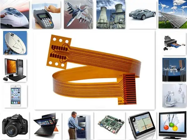
Introduction
Printed circuit boards (PCBs) form the foundation of electronics, providing the mechanical structure and electrical connections for components. The manufacturing process to transform raw materials into completed circuit boards is complex, requiring dozens of steps with specialized equipment.
This article provides a comprehensive overview of PCB fabrication including:
- Raw PCB materials like laminates, prepregs, foils and coatings
- Major fabrication steps for double-sided and multilayer boards
- Drilling processes for through holes and vias
- Conductive plating operations
- Imaging and etching of circuit traces
- Layer alignment and lamination methods
- Final finishing processes
- PCB assembly and population with components
- Quality inspection and test procedures
- Recent advances in fabrication technologies
- Comparison between prototype, low volume and mass production
- Examples of real-world PCBs and their construction
By understanding the sequences and options for manufacturing, electrical engineers can design optimized boards and collaborate effectively with fabrication partners.
Raw Materials for Constructing PCBs
A typical PCB comprises various specialized raw materials:
Substrate – The core dielectric material forms the main board layers. Common options:
- Woven fiberglass reinforced epoxy resin (FR-4)
- Ceramic-filled PTFE composites for high frequencies (Rogers RO3003)
- Cyanate ester or polyimide for high temperature (Panasonic TR-77)
Prepreg – Fiberglass fabric impregnated with partially cured epoxy. Bonds layers together under heat and pressure.
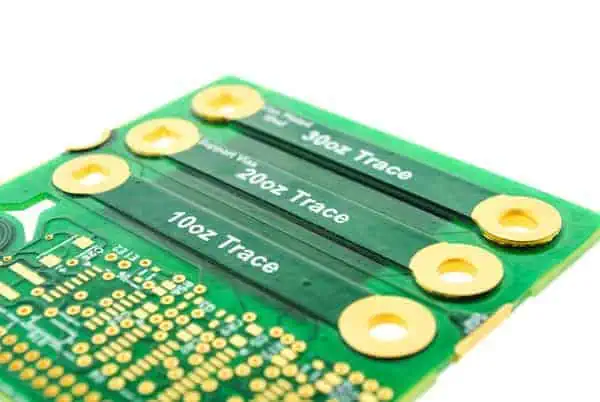
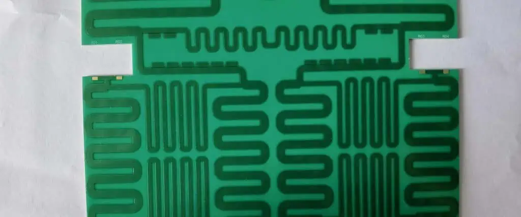
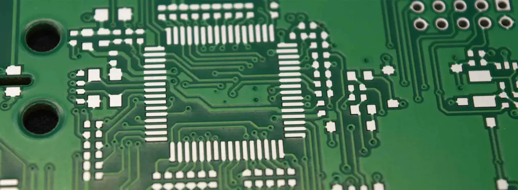
Metal Foil – Thin copper foil that is patterned into conductive traces and pads. Standard thicknesses range from 0.5 oz (17 μm) to 3 oz (105 μm).
Coatings – Protective layers such as solder mask, silkscreen, and plating finishes.
Bonding Film – Adhesives used in multilayer press lamination processes.
Via Fill – Plating resins or conductive pastes to plug vias in high density interconnect boards.
These raw PCB materials are fabricated together using specialized equipment and processes.
PCB Fabrication Process Overview
PCB manufacturing involves three main phases:
1. Circuit Imaging
- The conductive pattern of traces, pads and features are formed on each individual board layer
2. Layer Alignment and Lamination
- Individual layers are precisely aligned and bonded together into a multilayer board
3. Final Finishing
- Protective coatings are applied and the board edges finished
Dozens of individual steps are required within each phase during PCB fabrication. These generally fall into several broad categories:
- Imaging – transferring the circuit layout onto each layer
- Etching – selectively removing copper to form the circuit traces
- Drilling – creating holes for electrical connectivity between layers
- Plating – electroplating boards to build up conductive traces
- Bonding – laminating together the stack of circuitized layers
- Coatings – applying solder mask, legend, markings
- Finishing – trimming, beveling, testing finished boards
We will now examine each of these operations in greater detail.
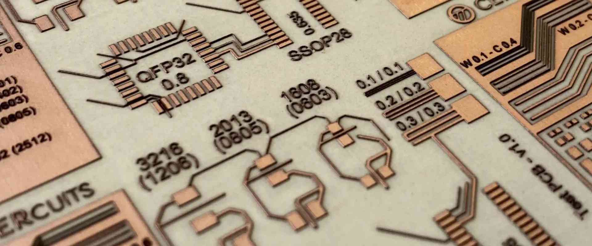
Imaging the Circuit Layout onto Layers
The first step in fabricating a circuit board is transferring the layout artwork onto each individual layer. This is accomplished using photographic imaging processes.
Photoresist Application
- Photosensitive epoxy coating spread across copper surfaces
- Adheres where cured, rinsed away where exposed
Imaging
- Mask or direct laser light transfers layout pattern
- Light either cures or degrades photoresist
Developing
- Uncured photoresist rinsed off with developer chemical
- Leaving behind circuit trace pattern in cured photoresist
Repeating this imaging process transfers the layout onto the copper layers. Next, etching forms the conductors.
Etching to Form Circuit Traces

With the photoresist imaging complete, the exposed copper is chemically etched away to form the conductive circuit traces and features.
Etchant Chemicals
- Usually cupric chloride or ammonium persulfate solutions
- Dissolve exposed copper but do not attack cured photoresist or substrate
Etching Process
- Boards submerged in etchant baths or sprayed
- Solution dissolves away exposed copper not protected by resist
- Leaves behind circuit pattern where resist remains
Photoresist Stripping
- Once etching completes, leftover photoresist is removed
- Usually washed off with hot caustic stripper solution
Etching therefore converts the imaging step into the physical conductive copper traces that form the circuitry.
Drilling Holes for Interlayer Connectivity
Holes drilled through the PCB layers provide electrical connectivity between traces on different layers. These are known as through holes or vias.
Mechanical Drilling
- Computer numerical control (CNC) drill machines
- High spindle speeds with small diameter drill bits
- Achieves moderate throughput on standard boards
- Pulsed UV lasers vapourize material in precise locations
- Allows high density microvias down to 0.005” diameter or less
- Used on complex multilayer boards
Plasma Etching
- Ionized gas plasma ablates material in circuit boards
- Enables extremely small microvia diameters down to 0.002”
- Reserved for most advanced HDI boards
The density of interconnections depends on the drilling and via formation capabilities.
Conductive Plating Processes
To form a continuous electrical connection through drilled holes and form durable conductive traces, boards are plated with copper and other metals.
Electroless Plating
- Auto-catalytic chemical deposition process
- Coats surfaces uniformly without electric current
- Provides initial thin copper layer (~0.1 mil)
Electrolytic Plating
- Thicker copper plated on top of electroless layer
- Uses electrical current to deposit up to 2 oz copper in holes/traces
Surface Finishing
- Coatings like ENIG (electroless nickel immersion gold)
- Provide solderability, corrosion resistance, contact surfaces
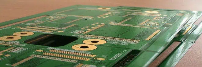
Plating deposits the conductive metal that carries signals across the finished boards.
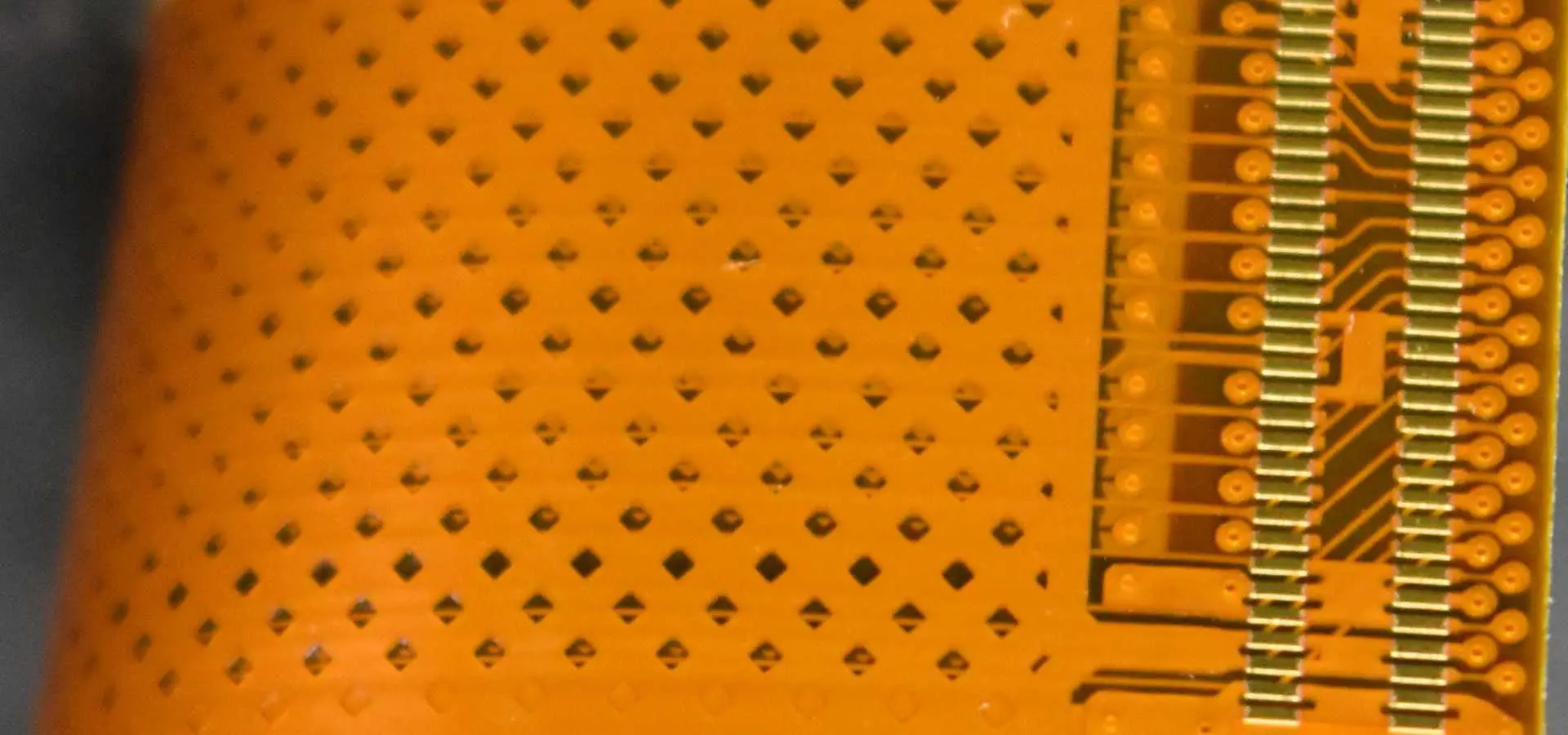
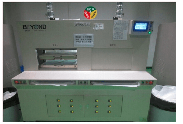
Layer Alignment and Lamination

To produce multilayer boards, individual internal and external circuitized layers are precisely aligned and fused together into the final board stackup.
Layer Alignment
- Optical recognition systems align layers
- Target registration accuracy under 0.003”
- Minimizes misalignment between layers
Lamination
- Aligned stack pressed under heat and pressure
- Melts dielectric prepreg materials to fuse together
- Bonds layers into solid multilayer board
Via Hole Plugging
- Prepregs flow to fill via holes during lamination
- Forms pad on each layer interconnected through hole
Careful alignment and lamination ensures reliable interconnections between the many layers.
Final PCB Finishing Steps
To complete board fabrication, various finishing operations are performed:
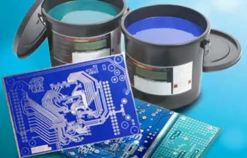
Solder Mask Application
- Liquid photoimageable coatings cover surface
- Provides solder bridges prevention and insulation
Silkscreen Legending
- Prints markings for components, logos, identifiers
- Improves appearance and aids manufacturing
Surface Finishes
- Coatings like ENIG, immersion tin or silver provides solderability
- OSP (organic solderability preservative) protects during storage
Edge Trimming
- Routers cut boards from panel edges
- High tolerance dimensional trimming
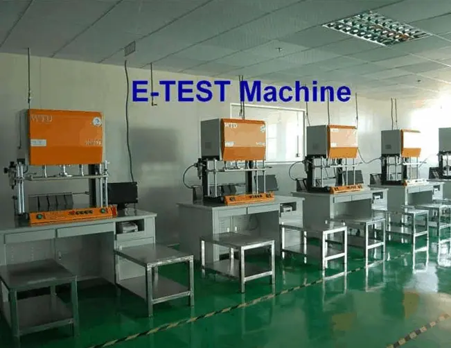
Electrical Testing
- In-circuit test (ICT) fixtures validate board assembly
- Confirms functioning before population
These finishing steps conclude the bare board fabrication process.
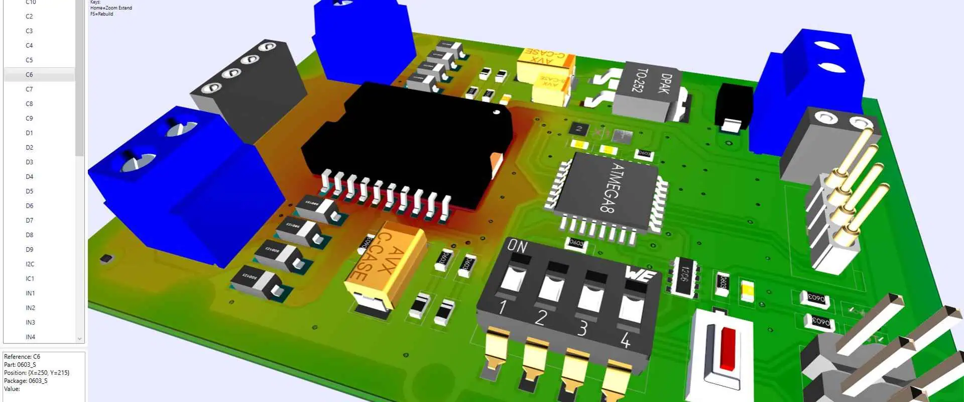
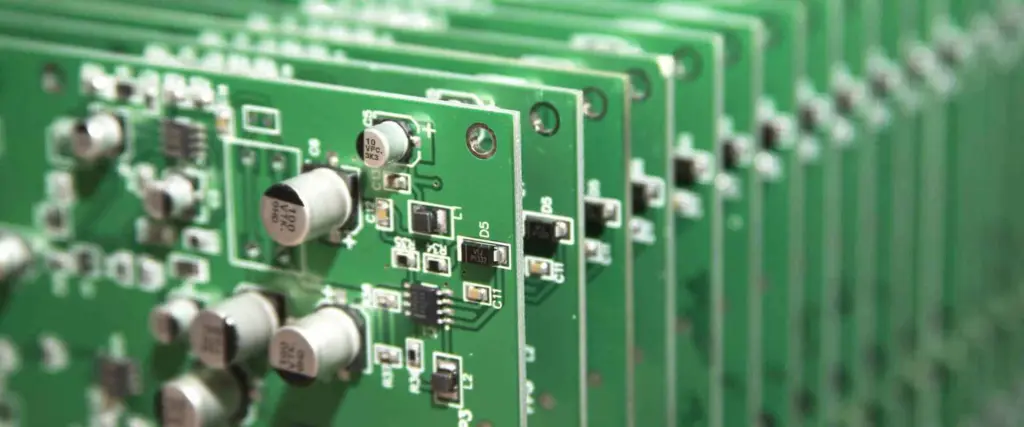
PCB Assembly and Component Population
To form a functional printed circuit board assembly (PCBA), electronic components must be added to the bare board through insertion and soldering:
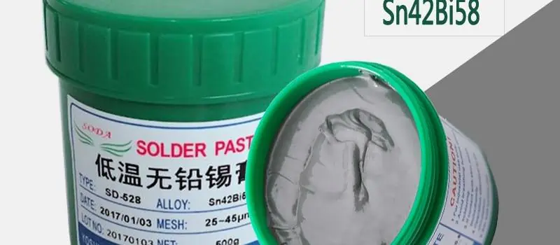
Screen Printing Solder Paste
- Solder paste deposited on pad areas
- Forms temporary adhesive to hold components
- Robotic placement systems position components precisely onto paste
- Accurately orients parts with great speed and repeatability
Reflow Soldering
- Heat melts solder paste to form permanent solder joints
- Stationary or conveyor ovens with heat profiles
- Alternative soldering methods exist (e.g. wave, drag)
Inspection and Test
- Optical and x-ray inspection of assemblies
- ICT fixtures confirm component placement and solder joints
- Validates part correctness and orientation
- Functionally tests populated board
This transforms the bare PCB into a functional electronic circuit assembly.
PCB Prototype vs. Production Comparison
Fabricating one-off prototypes differs substantially from volume production:
| Metric | Prototype PCB | Volume Production PCB |
|---|---|---|
| Process | Low volume lines | Dedicated mass production |
| Materials | Small sheets | Large panel sizes |
| Equipment | Lower throughput | Faster, automated |
| Testing | Basic electrical | Full ICT and functional test |
| Accuracy | Looser tolerances | Tighter tolerances |
| Lead Time | 5-10 days | 4+ weeks |
| Cost per board | High | Low |
In summary, prototypes prioritize fast turnaround while volume production maximizes efficiency and consistency.
Recent Advances in PCB Fabrication
Ongoing advances provide more capabilities:
HDI Technology
- Laser drilled microvias combined with thin dielectrics and trace widths enable further miniaturization
3D Printing
- Additive processes fabricate multilayer boards from liquid Polymers and inks
- Enables greater design freedom
Embedded Components
- Passive components inserted into inner layers
- Saves space and simplifies assembly
Flex/Rigid Flex
- Combines flexible polyimide films with standard laminate layers
- Foldable and shapeable boards
Board on Chip
- Entire PCBs fabricated directly onto silicon through semiconductor processes
- Ultimate space savings
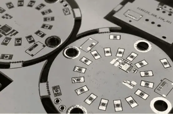
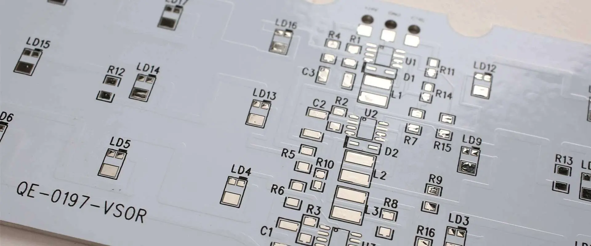
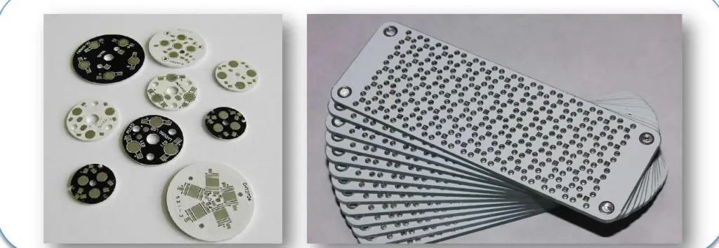
Real-World PCB Fabrication Examples
Here are some examples highlighting the manufacturing processes:
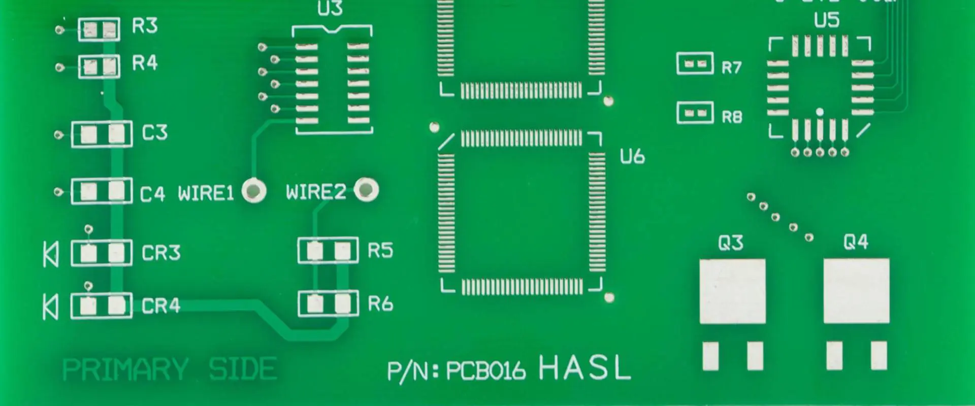
6-Layer Server Motherboard
- Glass-epoxy FR-4 laminate multilayer
- ~0.062” thick
- Mechanical through-hole drilling
- Plated copper traces and barrel-plated through holes
- LPI solder mask and silkscreen
- Lead-free HASL surface finish
- Wave soldering for mass assembly
16-Layer HDI Telecom Switch PCB
- High frequency PTFE-ceramic composite material
- Complex layer stackup with >150 um line widths/spaces
- Blinds and buried vias ablated by UV laser
- Copper electroplating to fill microvias and traces
- Stencil printed solder paste and SMT assembly
- Functional test and boundary scan
Flexible Wearable Health Tracker
- Flex-rigid construction combining polyimide and FR-4
- Flex section bends to contour body
- Adhesiveless lamination for flex layer bonding
- Plasma etching forms microvias in flex layers
- LDS laser activation for polymer plating
- Inkjet solder mask deposition
- ENIG finish, 01005 passives, micro-BGA packages
These case studies showcase the broad range of PCB manufacturing techniques tailored to meet diverse product needs.
Frequently Asked Questions
Here are some common questions surrounding PCB fabrication:
Q: What are the key differences between double-sided vs multilayer PCB construction?
Double-sided boards involve only a single substrate laminated on both sides with copper foil. Multilayer boards fuse together several laminate and prepreg layers for interlayer connectivity.
Q: How many drill bits are used to drill the holes in multilayer PCBs?
A large multilayer board might utilize 50-100 or more progressively larger bit sizes to sequentially increase each hole diameter from the starting drill through to the final size.
Q: What are common defects found during post-etch inspection?
Potential defects include underetching, overetching, nicks, scoring, pinholes, presence of debris, incomplete curing, and photoresist adhesion problems.
Q: What is the function of solder mask on the surface of PCBs?
Solder mask serves as a protective coating preventing solder bridges, providing insulation, and guarding against environmental corrosion and dendrite growth during operation.
Q: How accurate is layer-to-layer alignment in multilayer boards?
Alignment accuracy during lamination is generally around 0.003” for standard density boards. Even greater precision below 0.001” is achievable with advanced processes.
Conclusion
Printed circuit board manufacturing integrates an enormous range of chemical, mechanical and electrical processes spanning fabrication, assembly and test. By understanding the sequences required to transform raw materials into fully functional PCBs populated with components, engineers can optimally design boards for these manufacturing processes. A strong comprehension of PCB fabrication technologies enables effective collaboration throughout the electronics product development cycle.