Gerber files represent a critical standard in electronic design, serving as a universal format for PCB manufacturing documentation. While primarily used for production, these files can also become powerful tools for design reconstruction and modification in advanced PCB design software like Altium Designer.
Q1: Can I Completely Recreate a PCB Design from a Gerber File?
A1: While possible, complete recreation is challenging. Gerber files provide visual and manufacturing information but lack complete schematic and component details. Expect partial reconstruction with potential manual intervention.
Q2: What Are the Primary Limitations of Gerber File Editing?
A2: Limitations include incomplete layer information, potential loss of precise design intent, challenges in reconstructing complex geometries, and absence of original component metadata.
Q3: How Accurate Can Gerber File Reconstruction Be?
A3: Reconstruction accuracy varies, typically ranging from 70-90% depending on design complexity, file quality, and available supplementary documentation.
Q4: Are There Legal Considerations in Reproducing PCB Designs?
A4: Yes, always respect intellectual property rights. Ensure you have proper authorization before attempting to reproduce or modify proprietary PCB designs.
Q5: What Skills Are Required for Effective Gerber File Editing?
A5: Successful editing requires proficiency in PCB design software, understanding of electronic design principles, attention to detailed geometric reconstruction, and comprehensive design rule knowledge.
Conclusion
Editing PCB designs using Gerber files in Altium represents a sophisticated process combining technical expertise, advanced software capabilities, and meticulous attention to design reconstruction strategies. While challenging, it offers powerful opportunities for design analysis, modification, and preservation.
Printed Circuit Board (PCB) etching is a critical process in electronics manufacturing that requires meticulous attention to detail and precision. This comprehensive guide will explore the intricate world of testing etching chops through advanced map making techniques, providing engineers, technicians, and electronics enthusiasts with a deep understanding of the methodology, challenges, and best practices.
Understanding PCB Etching Fundamentals
The Science Behind PCB Etching
PCB etching is a chemical process that selectively removes copper from a substrate to create precise circuit patterns. The etching chops, or areas of copper removal, are crucial in determining the accuracy and quality of the final printed circuit board.
Key Components of the Etching Process
Etching Materials and Chemicals
The etching process typically involves several critical components:
Emerging technologies are revolutionizing PCB map making through:
Predictive defect analysis
Automated design optimization
Real-time process monitoring
Safety and Environmental Considerations
Strip film etching line
Handling Etching Chemicals
Safety Protocols
Personal protective equipment (PPE)
Proper chemical storage
Waste disposal regulations
Environmental Compliance
Chemical neutralization techniques
Recycling of etching solutions
Minimizing chemical waste
Frequently Asked Questions (FAQ)
Q1: What is the most critical factor in PCB etching chop accuracy?
A1: The most critical factor is the precision of your digital design and the quality of the resist material. Accurate CAD files and high-resolution photoresist application are key to achieving precise etching chops.
Q2: How often should etching equipment be calibrated?
A2: Professional facilities should calibrate etching equipment quarterly, with monthly preliminary checks. For smaller operations, bi-annual calibration is typically sufficient.
Q3: Can I reuse etching solutions?
A3: Etching solutions can be reused, but their effectiveness diminishes with each use. Implement a systematic monitoring process to track solution concentration and replace when performance degrades.
Q4: What are the signs of a poor etching process?
A4: Indicators include inconsistent line widths, rough board edges, copper residue, incomplete pattern transfer, and visible under or over-etching.
Q5: How do environmental conditions affect etching?
A5: Temperature, humidity, and chemical concentration significantly impact etching quality. Maintain a stable environment with controlled temperature (20-25°C) and minimal humidity fluctuations.
Conclusion
Mastering PCB etching chops through advanced map making requires a multifaceted approach combining technological expertise, precise measurement, and continuous learning. By implementing the strategies outlined in this guide, professionals can achieve exceptional results in printed circuit board manufacturing.
Surface finishes: Protect exposed copper and improve solderability
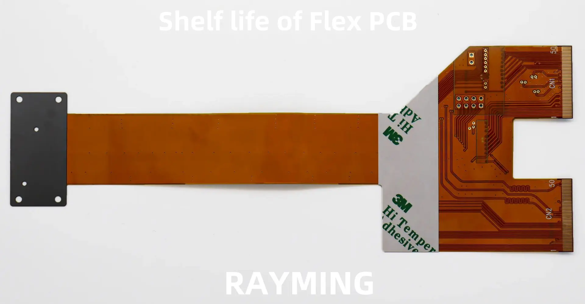
Factors Affecting Flex PCB Shelf Life
The shelf life of Flexible PCBs can be influenced by various factors. Understanding these factors is crucial for proper storage and handling.
1. Material Composition
The materials used in Flex PCBs play a significant role in determining their shelf life. Here’s a breakdown of common materials and their typical shelf lives:
Material
Typical Shelf Life
Notes
Polyimide
1-2 years
More resistant to environmental factors
Polyester
6-12 months
Less resistant to humidity and temperature changes
Proper handling and packaging can significantly extend the shelf life of Flex PCBs:
Use of moisture-barrier bags
Inclusion of desiccants and humidity indicator cards
Proper labeling with date of manufacture and storage recommendations
Minimizing physical stress during storage and transportation
Typical Shelf Life of Flex PCBs
The shelf life of Flex PCBs can vary widely depending on the factors mentioned above. However, here’s a general guideline:
Type of Flex PCB
Typical Shelf Life
Notes
Standard polyimide-based
12-24 months
Under optimal storage conditions
Polyester-based
6-12 months
More sensitive to environmental factors
High-reliability (space/medical grade)
24-36 months
Stricter manufacturing and storage standards
With sensitive components
6-12 months
Depends on the most sensitive component
It’s important to note that these are general guidelines, and actual shelf life can vary based on specific materials, manufacturing processes, and storage conditions.
Extending the Shelf Life of Flex PCBs
There are several strategies that can be employed to extend the shelf life of Flex PCBs:
1. Proper Storage Techniques
Use climate-controlled storage areas
Implement proper inventory management (FIFO – First In, First Out)
Use specialized packaging materials (moisture-barrier bags, desiccants)
2. Regular Inspection and Testing
Implement a schedule for visual inspections
Conduct electrical testing on a sample basis
Use specialized equipment like moisture analyzers
3. Repackaging and Rebaking
Repackage PCBs in fresh moisture-barrier bags periodically
Use baking processes to remove absorbed moisture when necessary
4. Surface Finish Selection
Choose surface finishes that offer longer shelf life:
Using Flex PCBs beyond their recommended shelf life can lead to various issues:
1. Solderability Problems
Poor wetting during soldering
Increased risk of solder joint failures
2. Delamination
Separation of layers due to adhesive degradation
Can lead to electrical and mechanical failures
3. Oxidation
Copper traces may oxidize, leading to connectivity issues
Can affect the performance of surface-mounted components
4. Mechanical Issues
Reduced flexibility
Increased risk of cracks or breaks during assembly or use
Best Practices for Managing Flex PCB Shelf Life
To ensure the quality and reliability of Flex PCBs, consider the following best practices:
Implement a robust inventory management system
Train staff on proper handling and storage procedures
Maintain detailed records of manufacturing dates and storage conditions
Develop a testing and inspection protocol for aged PCBs
Work closely with suppliers to understand and optimize shelf life
Consider just-in-time manufacturing to minimize storage time
Conclusion
Understanding and managing the shelf life of Flex PCBs is crucial for ensuring the quality and reliability of electronic products. By considering factors such as material composition, environmental conditions, and storage practices, manufacturers and users can maximize the usable life of these versatile components. Regular inspection, proper handling, and adherence to best practices can help mitigate the risks associated with using aged Flex PCBs and ensure optimal performance in the final application.
Frequently Asked Questions (FAQ)
1. How can I tell if a Flex PCB has exceeded its shelf life?
While it’s not always visually apparent, signs that a Flex PCB may have exceeded its shelf life include:
If you suspect a Flex PCB has exceeded its shelf life, it’s best to conduct electrical testing and consult with the manufacturer before use.
2. Can I use a Flex PCB that has exceeded its recommended shelf life?
It’s generally not recommended to use Flex PCBs that have exceeded their shelf life, as it can lead to reliability issues. However, if necessary, you may be able to recondition the PCB through processes like baking to remove moisture or re-finishing the surface. Always consult with the manufacturer and conduct thorough testing before using an aged Flex PCB in a critical application.
3. How does the shelf life of Flex PCBs compare to rigid PCBs?
Flex PCBs typically have a shorter shelf life compared to rigid PCBs due to their more sensitive materials and construction. While rigid PCBs made with FR-4 can often last 2-5 years under proper storage conditions, Flex PCBs usually have a shelf life of 1-2 years. The difference is primarily due to the flexible substrate materials and adhesives used in Flex PCBs, which are more susceptible to environmental factors.
4. Are there any industry standards for Flex PCB shelf life?
While there isn’t a single, universally accepted standard for Flex PCB shelf life, several industry guidelines provide recommendations. These include:
IPC-1601: Printed Board Handling and Storage Guidelines
IPC-6013: Qualification and Performance Specification for Flexible/Rigid-Flexible Printed Boards
JEDEC J-STD-033: Handling, Packing, Shipping and Use of Moisture/Reflow Sensitive Surface Mount Devices
These standards provide guidance on storage conditions, handling procedures, and moisture sensitivity levels that can impact shelf life.
5. How does the application of the Flex PCB affect its shelf life considerations?
The intended application of a Flex PCB can significantly influence shelf life considerations:
High-reliability applications (e.g., aerospace, medical devices) may require stricter storage conditions and shorter shelf life limits to ensure peak performance.
Consumer electronics may have more lenient shelf life requirements but should still adhere to best practices.
Applications involving extreme environments (high temperature, high humidity) may necessitate more frequent replacement of stored PCBs.
Products with long service lives may require special considerations for long-term storage of spare or replacement Flex PCBs.
Always consider the specific requirements of your application when determining appropriate shelf life limits and storage conditions for Flex PCBs.
When it comes to cost, Flex PCBs are generally more expensive than rigid PCBs. However, the cost difference can vary significantly based on various factors. Let’s break down the cost comparison:
As we can see from the table, Flex PCBs typically have higher initial costs due to more expensive base materials and a more complex manufacturing process.
Long-term Costs
While the initial costs of Flex PCBs are higher, it’s important to consider the long-term costs and benefits:
Cost Factor
Rigid PCB
Flex PCB
Replacement Frequency
Higher
Lower
Maintenance Costs
Moderate
Lower
Space Efficiency
Lower
Higher
Weight-related Costs
Higher
Lower
In many applications, the long-term benefits of Flex PCBs can offset their higher initial costs.
Factors Influencing Flex PCB Costs
Several factors contribute to the overall cost of Flex PCBs. Understanding these can help in making informed decisions and potentially reducing costs.
1. Material Selection
The choice of base material significantly impacts the cost of Flex PCBs. Common materials include:
Material
Cost Level
Flexibility
Temperature Resistance
Polyimide
High
Excellent
Excellent
Polyester
Moderate
Good
Moderate
PTFE
Very High
Good
Excellent
Polyimide is the most commonly used material due to its excellent properties, but it’s also more expensive than alternatives like polyester.
2. Circuit Complexity
The complexity of the circuit design directly affects the cost. Factors include:
Number of layers
Circuit density
Number of components
More complex designs require more sophisticated manufacturing processes, increasing the overall cost.
3. Production Volume
Like most manufacturing processes, economies of scale apply to Flex PCB production:
Production Volume
Cost per Unit
Low (< 100 units)
High
Medium (100-1000 units)
Moderate
High (> 1000 units)
Low
Larger production runs can significantly reduce the per-unit cost of Flex PCBs.
4. Manufacturing Process
The manufacturing process for Flex PCBs is more complex than for rigid PCBs, contributing to higher costs. Key steps include:
Higher quality standards typically result in increased testing costs but can lead to better long-term performance and reliability.
Cost-Saving Strategies for Flex PCBs
While Flex PCBs are generally more expensive than rigid PCBs, there are strategies to optimize costs:
1. Design Optimization
Efficient design can significantly reduce costs:
Minimize the number of layers
Optimize component placement
Reduce the overall size of the PCB
2. Material Selection
Choosing the right material for your specific application can help balance cost and performance:
Use polyester for less demanding applications
Reserve polyimide for high-performance needs
3. Volume Production
As mentioned earlier, increasing production volume can substantially reduce per-unit costs.
4. Prototype Carefully
Invest time and resources in prototyping to avoid costly design changes later in the production process.
5. Choose the Right Manufacturer
Select a manufacturer with experience in Flex PCB production. Their expertise can help optimize the manufacturing process and reduce costs.
When is the Higher Cost of Flex PCBs Justified?
Despite their higher initial costs, Flex PCBs can be more cost-effective in certain scenarios:
Space-constrained applications
Applications requiring frequent board flexing
Weight-sensitive designs (e.g., aerospace)
Harsh environments with vibration or temperature fluctuations
Products with complex 3D geometries
In these cases, the unique properties of Flex PCBs can provide value that outweighs their higher upfront costs.
Future Trends in Flex PCB Costs
As technology advances, we can expect changes in Flex PCB costs:
Improved manufacturing processes may reduce production costs
New materials might offer better cost-performance ratios
Increased adoption could lead to economies of scale, potentially lowering overall costs
Advancements in design software may optimize Flex PCB designs, reducing material waste and costs
Conclusion
While Flex PCBs are generally more expensive than rigid PCBs, their unique properties and potential long-term benefits can justify the higher cost in many applications. By understanding the factors that influence Flex PCB costs and implementing cost-saving strategies, it’s possible to optimize the use of this technology effectively.
The decision to use Flex PCBs should be based on a comprehensive analysis of both short-term and long-term costs, as well as the specific requirements of your application. In many cases, the flexibility, reliability, and space-saving characteristics of Flex PCBs can provide value that outweighs their higher initial cost.
As technology continues to evolve, we can expect further developments in Flex PCB manufacturing that may help reduce costs and expand their applications across various industries.
FAQ
Q: Are Flex PCBs always more expensive than rigid PCBs? A: Generally, yes. Flex PCBs typically have higher initial costs due to more expensive materials and a more complex manufacturing process. However, in some applications, their long-term benefits can offset the higher upfront costs.
Q: How much more expensive are Flex PCBs compared to rigid PCBs? A: The cost difference can vary widely depending on factors such as design complexity, materials used, and production volume. Flex PCBs can be anywhere from 20% to 200% more expensive than comparable rigid PCBs.
Q: Can the cost of Flex PCBs be reduced? A: Yes, there are several strategies to optimize Flex PCB costs, including design optimization, careful material selection, increasing production volume, thorough prototyping, and choosing an experienced manufacturer.
Q: Are there any hidden costs associated with Flex PCBs? A: While not hidden, some costs that might be overlooked include specialized assembly processes, additional testing requirements, and potentially higher repair or rework costs if issues arise.
Q: Will Flex PCB costs decrease in the future? A: It’s possible. As manufacturing processes improve and adoption increases, we may see a reduction in Flex PCB costs. However, this will depend on factors such as material costs, technological advancements, and market demand.
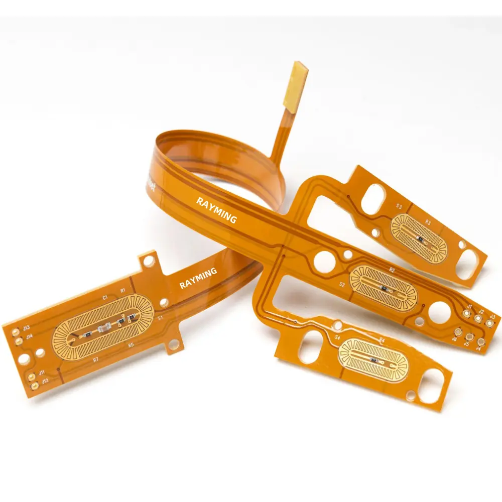
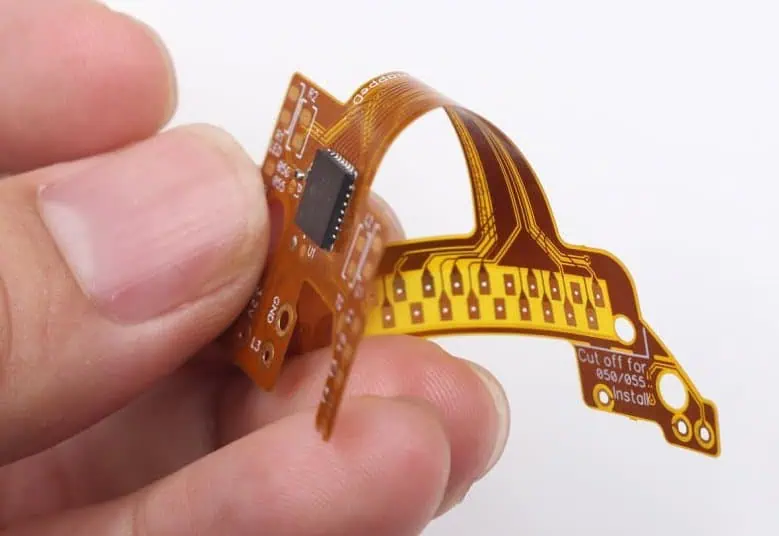
Flexible Printed Circuit Boards (PCBs) have revolutionized the electronics industry, offering numerous advantages such as reduced weight, space savings, and improved reliability. However, like any technology, they also come with their own set of drawbacks. This article delves into the various disadvantages of flexible PCBs, providing a comprehensive overview of the challenges faced by manufacturers, designers, and end-users when working with this technology.
Understanding Flexible PCBs
Before we explore the disadvantages, let’s briefly recap what flexible PCBs are and their basic characteristics.
Definition and Basic Characteristics
Flexible PCBs, also known as flex circuits, are electronic circuits mounted on flexible substrate materials. Unlike rigid PCBs, these circuits can bend, fold, and conform to various shapes, making them ideal for applications where space is at a premium or where the circuit needs to flex during use.
The higher costs associated with flexible PCBs stem from several factors:
Expensive raw materials: The polyimide or polyester substrates used in flexible PCBs are more expensive than the FR-4 material commonly used in rigid PCBs.
Complex manufacturing process: Producing flexible PCBs requires specialized equipment and more intricate processes, increasing production costs.
Design complexity: Designing flexible PCBs often takes more time and expertise, adding to the overall cost.
Limited Cost-Effectiveness for Low-Volume Production
While flexible PCBs can be cost-effective for high-volume production, they may not be economically viable for low-volume or prototype runs.
Design and Manufacturing Challenges
Complex Design Process
Designing flexible PCBs presents unique challenges that can be time-consuming and require specialized expertise.
Bend Radius Considerations
One of the critical aspects of flexible PCB design is accounting for the bend radius. Designers must ensure that the circuit can flex without damaging the conductive traces or components.
Table 2: Typical Minimum Bend Radii for Flexible PCBs
Flexible PCBs typically have fewer layers than their rigid counterparts, which can limit circuit complexity and functionality.
Table 3: Typical Layer Count Comparison
PCB Type
Typical Maximum Layers
Flexible PCBs
4-6
Rigid PCBs
16-32 (or more)
This limitation can force designers to make trade-offs between flexibility and circuit complexity.
Manufacturing Challenges
Handling and Processing Difficulties
The flexible nature of these PCBs can make them more challenging to handle during the manufacturing process. Issues such as warping, twisting, or folding can occur, potentially leading to defects or reduced yield rates.
Specialized Equipment Requirements
Manufacturing flexible PCBs requires specialized equipment, which can be a significant investment for PCB fabricators. This requirement can limit the number of manufacturers capable of producing flexible PCBs, potentially affecting lead times and costs.
Performance and Reliability Concerns
Thermal Management Issues
Flexible PCBs face unique challenges when it comes to heat dissipation.
Limited Heat Dissipation
The thin, flexible nature of these PCBs means they have less mass to absorb and dissipate heat compared to rigid PCBs. This can lead to potential overheating issues, especially in high-power applications.
While flexibility is a key advantage of these PCBs, it also introduces potential reliability issues.
Repeated Flexing
In applications where the PCB needs to flex repeatedly, there’s a risk of mechanical fatigue. This can lead to cracked traces, delamination, or component failure over time.
Table 5: Flex Life of Different Flexible PCB Constructions
Construction Type
Typical Flex Life (number of flexes)
Single-layer
1,000,000+
Double-layer
100,000 – 500,000
Multilayer
10,000 – 100,000
Environmental Sensitivity
Flexible PCBs can be more sensitive to environmental factors compared to rigid PCBs.
Moisture Sensitivity
The polyimide material commonly used in flexible PCBs can absorb moisture, potentially leading to delamination or changes in electrical properties.
Temperature Extremes
While flexible PCBs can generally withstand a wide range of temperatures, extreme conditions can cause issues such as dimensional changes or adhesive degradation.
Limited Repairability and Modification
Difficulty in Rework and Repair
Flexible PCBs present unique challenges when it comes to rework and repair.
Delicate Nature
The thin, flexible structure of these PCBs makes them more susceptible to damage during rework attempts. Standard repair techniques used for rigid PCBs may not be suitable or may risk further damage.
Limited Access
In applications where the flexible PCB is tightly integrated into a product, accessing the PCB for repairs can be extremely difficult or impossible without disassembling the entire product.
Challenges in Post-Production Modifications
Making changes to a flexible PCB after production can be more challenging compared to rigid PCBs.
Limited Real Estate
The compact nature of flexible PCB designs often means there’s little to no extra space for additional components or traces, making modifications difficult.
Maintaining Flexibility
Any modifications must be carefully considered to ensure they don’t compromise the PCB’s ability to flex as required in the application.
Prototype Assembling components onto flexible PCBs can be more challenging than with rigid PCBs.
Specialized Equipment
Standard pick-and-place machines may struggle with the flexible nature of the PCB, requiring specialized equipment or processes.
Soldering Difficulties
The heat-sensitive nature of flexible substrates can make soldering more challenging, requiring precise temperature control to avoid damaging the PCB.
Regulatory and Compliance Issues
EMI/EMC Challenges
Flexible PCBs can face unique challenges in meeting electromagnetic interference (EMI) and electromagnetic compatibility (EMC) requirements.
Limited Shielding Options
The thin, flexible nature of these PCBs can make it more difficult to incorporate effective EMI shielding compared to rigid PCBs.
Signal Integrity Issues
The flexible structure can potentially lead to signal integrity issues, especially in high-frequency applications, making it more challenging to meet EMC standards.
Environmental Compliance
While flexible PCBs themselves are often compliant with environmental regulations, the overall product may face challenges.
End-of-Life Considerations
The integrated nature of flexible PCBs in some applications can make them more difficult to separate and recycle at the end of a product’s life, potentially impacting compliance with e-waste regulations.
Conclusion
While flexible PCBs offer numerous advantages and have enabled many innovative product designs, it’s crucial to consider their disadvantages when deciding whether to use them in a particular application. From higher costs and design complexities to performance limitations and regulatory challenges, flexible PCBs present a unique set of trade-offs.
By understanding these disadvantages, engineers and product designers can make informed decisions about when and how to use flexible PCBs, balancing their benefits against their drawbacks to create optimal solutions for their specific applications.
Frequently Asked Questions (FAQ)
Q1: Are flexible PCBs more expensive than rigid PCBs?
A1: Yes, flexible PCBs typically have higher initial costs than rigid PCBs due to more expensive raw materials, complex manufacturing processes, and specialized design requirements. However, they can be cost-effective in high-volume production or where their unique properties provide significant advantages.
Q2: Can flexible PCBs handle high-power applications?
A2: Flexible PCBs generally have more limited heat dissipation capabilities compared to rigid PCBs, which can make them less suitable for high-power applications. However, design techniques such as using thicker copper layers or incorporating thermal management solutions can help mitigate this limitation in some cases.
Q3: How many times can a flexible PCB be bent?
A3: The number of times a flexible PCB can be bent depends on factors such as the PCB’s construction, the bend radius, and the specific materials used. Single-layer flex PCBs can often withstand over a million flexes, while multilayer designs may be limited to tens or hundreds of thousands of flexes.
Q4: Are all components compatible with flexible PCBs?
A4: Not all components are suitable for use with flexible PCBs. Small surface-mount devices (SMDs) are generally the most compatible, while larger or heavier components may be problematic. Through-hole components are typically avoided in flexible PCB designs as they can create stress points and limit flexibility.
Q5: Can flexible PCBs be repaired easily?
A5: Repairing flexible PCBs is generally more challenging than repairing rigid PCBs. Their delicate nature and often tightly integrated designs can make access difficult and increase the risk of damage during repair attempts. In many cases, it may be more practical to replace the entire flexible PCB rather than attempt a repair.
Understanding PCB pricing can be complex due to the numerous variables involved in the manufacturing process. RAYMING provides a comprehensive price comparison system that helps customers make informed decisions. This guide will walk you through the various factors affecting PCB costs and how to effectively compare prices using RAYMING‘s platform.
Q1: How accurate are RAYMING’s instant quotes compared to final pricing?
A1: RAYMING’s instant quotes are typically accurate within 5-10% of final pricing for standard specifications. Complex designs may require manual review for final pricing accuracy.
Q2: What factors can cause the biggest price variations in PCB manufacturing?
A2: The most significant price variations come from layer count, board size, material selection, and quantity. Special requirements like controlled impedance or blind/buried vias can also substantially impact pricing.
Q3: How does RAYMING handle price comparisons for non-standard specifications?
A3: For non-standard specifications, RAYMING provides initial estimates through the comparison tool and follows up with a detailed manual quote within 24 hours.
Q4: Can I get better pricing by combining different PCB designs in one order?
A4: Yes, RAYMING offers panel sharing options for multiple designs with similar specifications, potentially reducing costs by 15-25%.
Q5: What is RAYMING’s policy on price matching with competitors?
A5: RAYMING offers competitive price matching for identical specifications and quality levels, requiring documentation of the competitor’s quote for verification.
Conclusion
RAYMING’s PCB price comparison system provides a comprehensive tool for understanding and optimizing PCB manufacturing costs. By considering all variables and utilizing the available optimization strategies, customers can achieve the best balance of cost, quality, and delivery time for their specific needs.
Gold plating represents one of the most critical surface finishing processes in printed circuit board (PCB) manufacturing, providing essential protection and functionality to electronic components. This sophisticated electrochemical process applies a thin layer of gold to specific areas of the PCB, creating a corrosion-resistant, highly conductive surface that ensures reliable electrical connections and long-term performance.
Understanding Gold Plating in PCB Manufacturing
Gold plating in PCB production serves multiple vital functions beyond mere aesthetics. The primary purpose involves creating oxidation-resistant contact surfaces that maintain excellent electrical conductivity over extended periods. Unlike copper, which readily oxidizes when exposed to air and moisture, gold remains chemically inert under normal environmental conditions, making it ideal for critical connection points such as edge connectors, component pads, and test points.
The gold plating process typically involves depositing a thin layer of gold, usually ranging from 0.05 to 2.54 microns (2 to 100 microinches) in thickness, onto designated areas of the PCB. This seemingly minimal thickness provides substantial protection while maintaining cost-effectiveness, as gold remains one of the more expensive materials used in PCB manufacturing.
Types of Gold Plating Processes
PCB manufacturers employ several distinct gold plating techniques, each suited to specific applications and requirements. Hard gold plating, also known as electrolytic gold plating, involves depositing a relatively thick layer of gold (typically 1.27 to 2.54 microns) that contains small amounts of hardening agents such as cobalt or nickel. This process creates a durable surface capable of withstanding repeated insertions and mechanical stress, making it ideal for edge connectors and switches.
Soft gold plating, conversely, deposits pure gold without hardening additives, resulting in a more malleable surface excellent for wire bonding applications. The thickness typically ranges from 0.25 to 1.27 microns, providing adequate protection while maintaining the material properties necessary for reliable wire bond connections.
Electroless nickel immersion gold (ENIG) represents another popular approach, combining a nickel barrier layer with a thin immersion gold coating. This process offers excellent planarity and is particularly well-suited for surface mount technology applications where component placement accuracy is crucial.
The Gold Plating Process Steps
The gold plating process begins with thorough PCB preparation, including cleaning to remove any contaminants, oxides, or residues that might interfere with proper adhesion. This cleaning typically involves both chemical and mechanical methods to ensure optimal surface condition.
Following cleaning, the PCB undergoes a nickel plating step, which serves as a barrier layer between the copper substrate and the gold coating. Nickel prevents copper migration into the gold layer, which could compromise the gold’s protective properties and electrical performance. The nickel layer typically ranges from 1.27 to 5.08 microns in thickness.
The actual gold plating occurs through electrochemical deposition, where the PCB serves as the cathode in an electrolytic cell containing gold cyanide or gold sulfite solutions. Electric current drives gold ions from the solution onto the PCB surface, creating a uniform, adherent coating. Process parameters such as current density, temperature, pH, and plating time must be carefully controlled to achieve consistent results.
Critical Process Parameters
Temperature control plays a crucial role in gold plating quality, with most processes operating between 60-70°C (140-158°F). Higher temperatures can accelerate deposition rates but may also increase the risk of poor adhesion or grain structure issues. Lower temperatures generally produce finer grain structures but require longer plating times.
Current density directly affects deposition rate and gold layer characteristics. Typical current densities range from 0.5 to 2.0 amperes per square decimeter, with higher densities producing faster deposition but potentially compromising surface quality. Maintaining uniform current distribution across the PCB surface ensures consistent gold thickness and quality.
Solution chemistry requires constant monitoring and adjustment to maintain optimal plating conditions. Gold concentration, pH levels, and the presence of organic additives all influence the final coating properties. Regular solution analysis and replenishment help maintain consistent plating quality throughout production runs.
Quality Control and Testing
Gold plating quality assessment involves multiple testing methods to ensure specification compliance. Thickness measurements using X-ray fluorescence or cross-sectional microscopy verify that gold deposits meet dimensional requirements across the entire PCB surface.
Adhesion testing evaluates the bond strength between the gold layer and underlying nickel or copper substrates. Standard tests include tape adhesion tests and thermal cycling to simulate operational stresses that might cause coating failure.
Solderability testing ensures that gold-plated surfaces maintain their ability to form reliable solder joints. This testing becomes particularly important for surfaces that will undergo multiple thermal cycles during assembly and rework operations.
Porosity testing identifies potential defects in the gold coating that could allow corrosive agents to reach the underlying metal layers. Various methods, including electrolytic porosity tests, help identify coating integrity issues before final product shipment.
Applications and Benefits
Gold plating finds extensive application in high-reliability electronic systems where connection integrity is paramount. Aerospace and defense electronics commonly specify gold plating for critical connections due to its exceptional corrosion resistance and long-term stability. Medical devices also frequently utilize gold plating to ensure reliable operation in challenging environments.
Consumer electronics benefit from gold plating in applications such as memory card contacts, USB connectors, and audio/video interfaces where repeated insertions occur. The superior wear resistance of hard gold plating makes these connections reliable throughout their intended service life.
The benefits of gold plating extend beyond corrosion protection to include excellent electrical conductivity, thermal stability, and biocompatibility. These properties make gold plating suitable for applications ranging from implantable medical devices to high-frequency RF circuits where signal integrity is crucial.
Challenges and Considerations
Despite its advantages, gold plating presents several challenges that manufacturers must address. Cost considerations often drive decisions about where to apply gold plating, as the material expense can significantly impact overall PCB costs. Selective plating techniques help minimize gold usage while maintaining performance in critical areas.
Environmental regulations increasingly affect gold plating processes, particularly regarding cyanide-based plating solutions. Many manufacturers have transitioned to more environmentally friendly alternatives, though these may require process modifications to achieve equivalent performance.
Process control complexity increases with gold plating, as multiple parameters must be simultaneously monitored and adjusted to maintain quality. Automated process control systems help manage this complexity while ensuring consistent results across production volumes.
Future Developments
Ongoing research in gold plating technology focuses on reducing costs while maintaining or improving performance characteristics. Alternative gold alloys and deposition techniques show promise for specific applications, potentially offering cost advantages while meeting performance requirements.
Nanotechnology applications are exploring ultra-thin gold coatings that provide adequate protection with minimal material usage. These developments could significantly reduce gold plating costs while maintaining essential protective properties.
Environmental considerations continue driving innovation toward more sustainable plating processes and materials. Research into gold recovery and recycling from PCB manufacturing waste helps offset material costs while reducing environmental impact.
The common gold plating process for PCBs represents a sophisticated balance of chemistry, physics, and engineering that enables the reliable operation of countless electronic devices. Understanding these processes helps engineers and manufacturers make informed decisions about when and how to implement gold plating for optimal performance and cost-effectiveness.
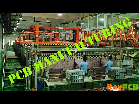
The manufacturing of specialized printed circuit boards (PCBs) represents one of the most complex challenges in modern electronics production. Unlike standard PCBs used in consumer electronics, special PCBs—including high-frequency boards, flexible circuits, rigid-flex assemblies, and boards designed for extreme environments—require sophisticated manufacturing approaches that balance performance, reliability, and cost-effectiveness. The optimization of these processes has become increasingly critical as industries demand higher performance from smaller, more complex electronic systems.
Understanding Special PCB Requirements
Special PCBs encompass a broad range of applications, each with unique manufacturing challenges. High-frequency PCBs used in telecommunications and radar systems require precise impedance control and minimal signal loss. Flexible PCBs for wearable devices and automotive applications must withstand repeated bending while maintaining electrical integrity. Medical device PCBs demand exceptional reliability and biocompatibility, while aerospace applications require boards that can operate in extreme temperatures and radiation environments.
The substrate materials alone present significant manufacturing complexities. While standard PCBs typically use FR-4 fiberglass, special applications may require polyimide for flexibility, PTFE-based materials for high-frequency performance, or ceramic substrates for thermal management. Each material brings distinct processing requirements, from different etching chemistries to specialized drilling techniques and unique lamination parameters.
Advanced Design for Manufacturing Principles
Optimizing special PCB manufacturing begins at the design stage through comprehensive design for manufacturing (DFM) analysis. This process involves close collaboration between design engineers and manufacturing specialists to identify potential production challenges before they impact yield or quality. For high-frequency applications, this means careful consideration of trace geometry, via placement, and ground plane continuity to maintain signal integrity throughout the manufacturing process.
Stackup optimization plays a crucial role in special PCB manufacturing. The arrangement of copper layers, dielectric materials, and their thicknesses must be precisely controlled to achieve desired electrical characteristics while remaining manufacturable. Advanced simulation tools help predict how manufacturing tolerances will affect final performance, allowing designers to build in appropriate margins while minimizing over-engineering.
Material selection optimization extends beyond basic electrical requirements to consider manufacturing compatibility. The coefficient of thermal expansion mismatch between different materials can cause registration issues during lamination, while some high-performance materials may require modified processing temperatures or atmospheres. Successful optimization requires understanding these interactions and designing stackups that achieve performance goals while remaining producible with high yield.
Precision Manufacturing Techniques
The manufacturing of special PCBs demands precision far beyond standard production capabilities. Drilling operations, for instance, must account for the unique properties of specialized substrates. PTFE-based materials can cause drill bit wandering due to their low friction coefficient, requiring specialized drill bits and modified drilling parameters. Polyimide flexible circuits need carefully controlled entry and exit materials to prevent tearing during drilling operations.
Etching processes for special PCBs often require customized chemistries and parameters. High-frequency boards may use thicker copper to reduce resistance, necessitating longer etch times and more aggressive chemistries that can affect fine-pitch features. Some materials are sensitive to certain etchants, requiring alternative processes or protective measures. The optimization of etch compensation becomes critical when working with mixed dielectrics that etch at different rates.
Lamination represents perhaps the most critical process in special PCB manufacturing. The combination of temperature, pressure, and time must be precisely controlled to achieve proper bonding while avoiding material degradation. Some high-performance materials have narrow processing windows, requiring sophisticated press control systems and careful monitoring. Vacuum lamination may be necessary for certain applications to eliminate voids that could affect electrical performance or reliability.
Quality Control and Testing Optimization
Special PCBs require enhanced quality control measures that go far beyond standard electrical testing. High-frequency boards need specialized test equipment capable of measuring impedance, insertion loss, and other RF parameters across their intended frequency range. This testing must be integrated into the manufacturing flow to catch deviations early, as rework options are often limited with exotic materials.
In-process monitoring becomes crucial for special PCB optimization. Real-time measurement of key parameters during manufacturing allows for immediate correction of drift conditions before they affect product quality. This might include continuous monitoring of etch rates, lamination temperature profiles, or drill registration accuracy. Statistical process control techniques help identify trends that could indicate equipment drift or material variation.
Non-destructive testing methods play an increasingly important role in special PCB manufacturing. Micro-sectioning for traditional cross-sectional analysis can damage expensive boards, making techniques like X-ray inspection, ultrasonic testing, and advanced optical inspection more valuable. These methods can detect internal defects, delamination, or material inconsistencies without compromising the product.
Process Flow Optimization
The manufacturing sequence for special PCBs often differs significantly from standard processes. Flexible circuits may require specialized handling fixtures throughout production to prevent damage from bending or stretching. Rigid-flex boards need careful planning of the fabrication sequence to protect flexible regions during processing of rigid areas.
Optimization of process flow considers the unique requirements of each manufacturing step and their interactions. For example, the thermal history of high-frequency materials can affect their electrical properties, requiring careful sequencing of heat-intensive operations. Some processes may need to be performed in controlled atmospheres to prevent oxidation or contamination of sensitive materials.
Automation plays a crucial role in optimizing special PCB manufacturing, but must be carefully implemented. Standard automation equipment may not be suitable for handling delicate flexible circuits or boards with non-standard thicknesses. Custom fixturing and handling systems are often necessary to maintain process control while protecting sensitive products.
Yield Improvement Strategies
Yield optimization for special PCBs requires a comprehensive approach that addresses both manufacturing defects and design-related issues. Pareto analysis of defect sources helps focus improvement efforts on the most impactful issues. Common challenges include registration problems between layers, material handling damage, and process-induced stress that can cause delamination or cracking.
Statistical analysis of manufacturing data helps identify the optimal process windows for each parameter. Design of experiments (DOE) techniques can efficiently explore the interaction between multiple variables to find optimal settings. This is particularly important for processes with narrow operating windows where small variations can significantly impact yield.
Preventive maintenance programs become even more critical for special PCB manufacturing due to the tight tolerances required. Equipment calibration schedules must account for the precision demands of specialized processes, and predictive maintenance techniques can help avoid unexpected failures that could damage expensive materials or compromise product quality.
Cost Optimization Strategies
While special PCBs inherently carry higher costs than standard products, careful optimization can significantly improve cost-effectiveness. Material utilization optimization through improved panel layouts can reduce waste of expensive substrates. This requires sophisticated nesting algorithms that account for the unique constraints of special materials, such as grain direction in flexible substrates or the location of fiberglass weave patterns.
Process optimization can reduce manufacturing time and improve throughput without compromising quality. This might involve optimizing cure cycles for specialized adhesives, reducing the number of process steps through innovative techniques, or improving equipment utilization through better scheduling algorithms.
Supply chain optimization becomes particularly important for special PCBs due to the specialized nature of materials and equipment. Long lead times for exotic materials require careful inventory management and demand forecasting. Strategic partnerships with suppliers can provide access to technical expertise and ensure priority allocation of limited materials.
Future Trends and Technologies
The optimization of special PCB manufacturing continues to evolve with advancing technology. Additive manufacturing techniques show promise for creating complex three-dimensional circuits that would be impossible with traditional subtractive methods. Digital printing of conductive inks could enable rapid prototyping and small-volume production of specialized circuits.
Artificial intelligence and machine learning are beginning to impact special PCB manufacturing through predictive quality control and process optimization. These technologies can identify subtle patterns in manufacturing data that indicate potential quality issues before they manifest as defects.
Advanced materials continue to push the boundaries of what’s possible in special PCB applications. New dielectric materials with improved properties, embedded components that integrate active devices within the PCB structure, and novel conductor materials all present both opportunities and manufacturing challenges that will require continued process optimization.
The optimization of manufacturing processes for special PCBs represents a continuous journey of improvement, driven by the ever-increasing demands of advanced electronic systems. Success requires a holistic approach that considers design, materials, processes, and quality control as integrated elements of a complex manufacturing system. As technology continues to advance, the ability to efficiently manufacture these specialized products will become an increasingly important competitive advantage in the electronics industry.
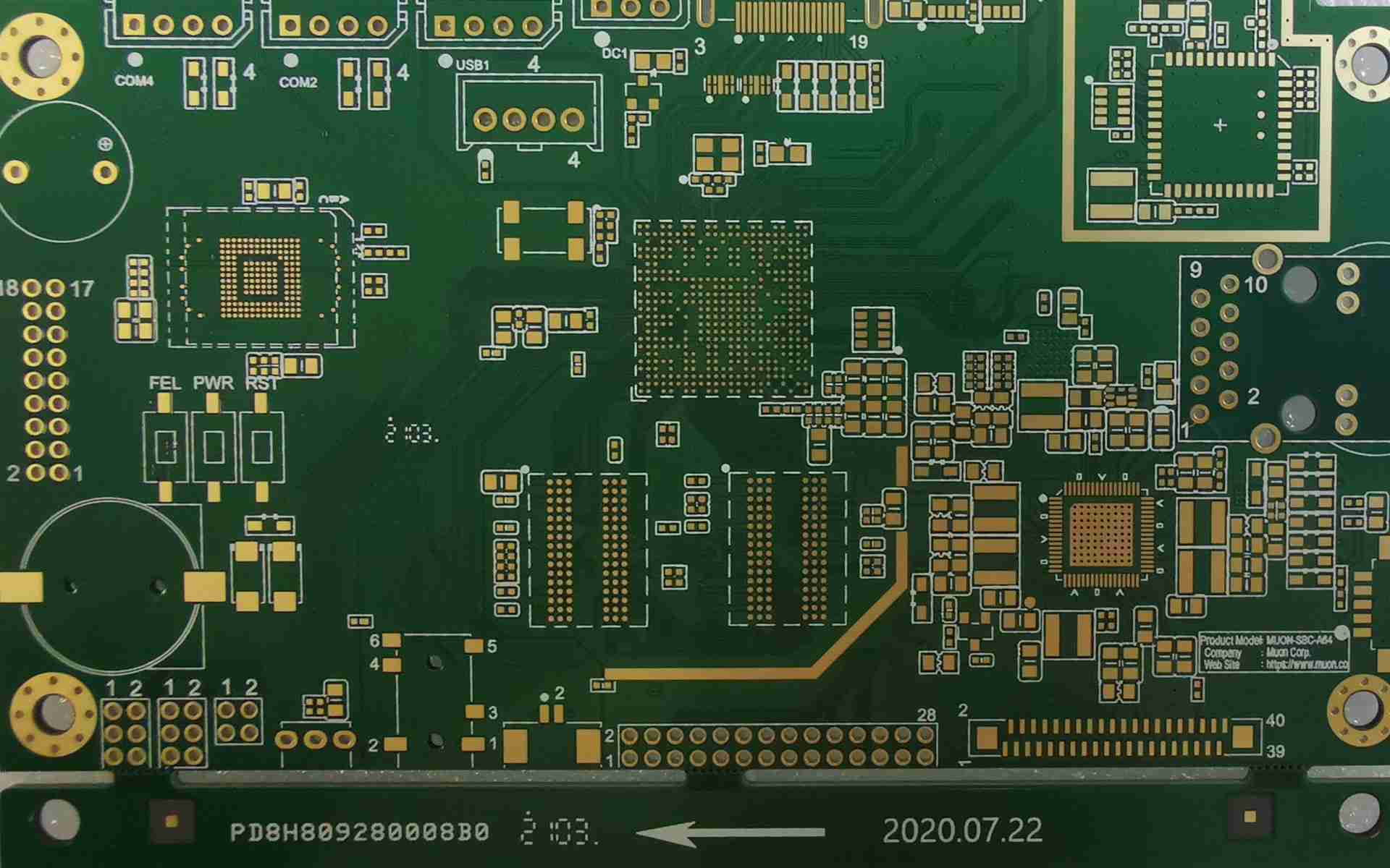
High Density Interconnect (HDI) technology has revolutionized the design and manufacturing of large, dense printed circuit boards (PCBs), enabling unprecedented levels of miniaturization and performance in modern electronic devices. As component densities continue to increase and form factors shrink, HDI layer stackup design becomes critical for achieving optimal electrical performance, manufacturing reliability, and cost-effectiveness in complex electronic systems.
Understanding HDI Technology Fundamentals
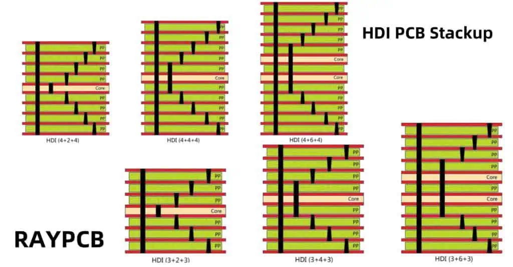
HDI PCBs are characterized by their use of microvias, buried vias, and sequential build-up layers that allow for significantly higher routing density compared to traditional PCB designs. The defining feature of HDI boards is the microvia structure, typically with diameters of 150 micrometers or less, which enables fine-pitch component placement and high-density routing. These microvias are formed through laser drilling, allowing for precise hole formation that would be impossible with mechanical drilling techniques.
The sequential lamination process used in HDI manufacturing allows for the creation of complex layer stackups with multiple build-up layers on each side of a core substrate. This approach enables designers to route high pin-count components like ball grid arrays (BGAs) and chip-scale packages (CSPs) while maintaining signal integrity and minimizing board real estate requirements.
Strategic Stackup Planning for Large Dense PCBs
When designing HDI stackups for large, dense PCBs, several fundamental principles must guide the planning process. The stackup must accommodate high-speed digital signals, power distribution requirements, thermal management considerations, and manufacturing constraints while maintaining mechanical stability across large board dimensions.
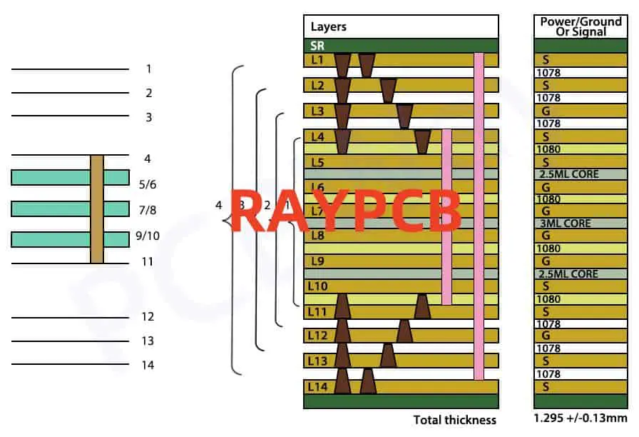
Layer count determination begins with component pin-out analysis and routing density calculations. Large dense PCBs often require 12 to 20+ layers to accommodate complex routing requirements. The distribution of these layers between signal, power, and ground planes requires careful optimization to ensure adequate power delivery, signal isolation, and electromagnetic compatibility.
Power distribution network (PDN) design becomes particularly challenging in large HDI boards due to increased power consumption and the need for multiple voltage rails. The stackup must incorporate sufficient power and ground planes positioned strategically to minimize impedance and provide adequate decoupling. Typically, this involves dedicating 30-40% of the layer count to power distribution, with careful attention to plane pairing and via transitions.
Signal Integrity Considerations in HDI Stackups
High-speed signal routing in large dense HDI PCBs requires meticulous attention to controlled impedance design and crosstalk mitigation. The stackup must provide consistent impedance profiles across all signal layers while accommodating various signal types including single-ended, differential pairs, and high-speed serial interfaces.
Dielectric selection plays a crucial role in achieving target impedance values while maintaining low loss characteristics for high-frequency signals. Modern HDI designs often employ low-loss dielectric materials with stable dielectric constants across temperature and frequency ranges. The choice between different prepreg and core materials must balance electrical performance with manufacturing feasibility and cost considerations.
Via transitions present unique challenges in HDI designs, particularly when signals must traverse multiple build-up layers. The stackup design must minimize via stub lengths through the use of back-drilling or blind/buried via structures. Sequential via transitions, where signals move from one build-up layer to another through carefully planned via chains, require precise impedance modeling to prevent signal degradation.
Thermal Management Integration
Large dense PCBs generate significant heat that must be efficiently dissipated to maintain component reliability and performance. The HDI stackup design must incorporate thermal management features including thermal vias, heat spreading planes, and strategic copper balancing to facilitate heat transfer from high-power components to heat sinks or thermal interfaces.
Thermal via design in HDI stackups requires careful coordination with the electrical routing to avoid interference while maximizing thermal conductivity. Dense arrays of small thermal vias often prove more effective than larger, less numerous vias for heat transfer from surface-mounted components to internal ground planes or dedicated thermal layers.
Copper balancing becomes critical in large HDI boards to prevent warpage during manufacturing and operation. The stackup must maintain relatively uniform copper distribution across layers while accommodating varying routing densities in different board regions. This often requires the addition of copper fills, hatching patterns, or dummy features in lightly routed areas.
Manufacturing Constraints and Design Rules
HDI manufacturing imposes specific constraints that must be considered during stackup design. Sequential lamination processes require careful attention to registration tolerances, especially in large boards where thermal expansion can cause significant dimensional variations. The stackup design must accommodate these manufacturing realities through appropriate design margins and tolerance allocations.
Microvia formation through laser drilling requires specific material combinations and thickness limitations. Each build-up layer must conform to manufacturer capabilities regarding minimum via sizes, aspect ratios, and capture pad dimensions. These constraints often influence layer thickness selection and routing strategies throughout the stackup.
Aspect ratio management becomes particularly important in thick HDI stackups. While mechanical drilling can achieve higher aspect ratios for through-hole vias, the combination of through-holes and microvias in a single stackup requires careful optimization to ensure reliable via formation and plating. This often necessitates the use of staggered via structures or multiple via transitions to connect signals across the full board thickness.
Advanced HDI Architectures
Modern large dense PCBs often employ advanced HDI architectures including any-layer HDI (ALDI) and embedded component technologies. ALDI allows via formation between any two layers in the stackup, providing maximum routing flexibility but requiring sophisticated manufacturing processes and design verification.
Embedded passive components, including resistors and capacitors built directly into the PCB substrate, can be integrated into HDI stackups to further increase functional density. This approach requires specialized materials and manufacturing processes but can significantly reduce component count and improve electrical performance through reduced parasitic effects.
Package substrate integration represents another advanced approach where the PCB stackup is designed to accommodate flip-chip mounting of bare die or advanced packaging technologies. This requires extremely fine feature sizes and specialized materials but enables unprecedented integration levels for high-performance applications.
Design Verification and Testing Strategies
Large dense HDI PCBs require comprehensive design verification including electromagnetic simulation, thermal analysis, and mechanical stress evaluation. The complex stackup structures and high component densities make traditional design rule checking insufficient for ensuring reliable operation.
Signal integrity simulation must account for the complex via transitions, layer changes, and coupling effects present in HDI stackups. Three-dimensional electromagnetic modeling becomes essential for accurate prediction of high-frequency behavior and optimization of critical signal paths.
Power integrity analysis must verify adequate power delivery across all voltage rails while accounting for the distributed nature of power distribution in large boards. This includes evaluation of voltage ripple, transient response, and electromagnetic interference from power distribution networks.
Manufacturing design for testability becomes challenging in dense HDI designs due to limited test point accessibility and high routing density. The stackup design must incorporate provisions for in-circuit testing, boundary scan testing, and functional verification while maintaining signal integrity and routing efficiency.
Cost Optimization Strategies
HDI manufacturing costs scale significantly with layer count, via complexity, and feature density. Effective stackup design must balance performance requirements with cost constraints through strategic material selection, via optimization, and manufacturing process selection.
Selective HDI implementation, where high-density features are used only in areas requiring maximum routing density, can provide cost savings while maintaining overall board functionality. This approach requires careful interface design between HDI and conventional PCB sections but can significantly reduce manufacturing complexity and cost.
The future of HDI layer stackup design for large dense PCBs continues to evolve with advancing materials technology, manufacturing capabilities, and electronic system requirements. Success in this field requires careful integration of electrical, thermal, mechanical, and manufacturing considerations to achieve optimal performance, reliability, and cost-effectiveness in increasingly complex electronic systems.
High-Density Interconnect (HDI) technology has revolutionized printed circuit board (PCB) design and manufacturing, enabling unprecedented levels of miniaturization and functionality. This comprehensive guide explores the latest developments in HDI technology, design considerations, and best practices for achieving optimal miniaturization in modern PCB designs.
Greater design flexibility and component placement options These advantages make HDI essential for modern electronic devices requiring high performance in small form factors.
2. How does HDI technology impact manufacturing costs?
HDI manufacturing costs are influenced by several factors:
More sophisticated processing equipment requirements
More stringent quality control requirements However, these costs are often offset by the reduced board size and improved performance.
3. What are the key design considerations for HDI PCBs?
Critical design considerations include:
Stack-up planning and impedance control
Microvia placement and structure
Component density and placement optimization
Power distribution network design
Thermal management strategies Careful attention to these factors is essential for successful HDI implementation.
4. How can reliability be ensured in HDI designs?
Reliability in HDI designs is achieved through:
Proper material selection for the application
Careful stack-up design and via structure planning
Comprehensive thermal management strategies
Thorough testing and validation procedures
Adherence to manufacturing design rules Regular testing and validation throughout the design process is crucial.
5. What future developments are expected in HDI technology?
The future of HDI technology includes:
Further miniaturization of features and components
Integration of embedded components
Advanced materials for improved performance
3D packaging and integration
Novel manufacturing processes These developments will enable even greater levels of integration and performance.
Conclusion
High-Density Interconnect technology continues to evolve, pushing the boundaries of PCB miniaturization and performance. Success in HDI design requires a thorough understanding of materials, processes, and design constraints, along with careful consideration of reliability and cost factors. As electronic devices continue to demand higher performance in smaller packages, HDI technology will remain crucial for meeting these challenges. The future of HDI lies in the successful integration of emerging technologies and materials while maintaining focus on manufacturability and reliability.