Aluminum PCB Stackup: Balancing Thermal Conductivity and Signal Integrity

aluminum substrate pcb

Introduction

In the ever-evolving world of electronics, thermal management and signal integrity have become critical factors in design and performance. Enter the Aluminum PCB Stackup, a innovative solution that addresses these challenges head-on. This article delves into the intricacies of Aluminum PCB Stackups, exploring how they balance thermal conductivity and signal integrity to meet the demands of modern electronic devices.

Aluminum PCBs have gained significant traction in recent years, particularly in applications requiring efficient heat dissipation. The importance of Aluminum PCB Stackup in modern electronics cannot be overstated, as it offers a unique combination of thermal management and electrical performance. As we push the boundaries of what’s possible in electronic design, striking the right balance between these two critical aspects becomes increasingly crucial.

What is an Aluminum PCB Stackup?

Definition and Structure

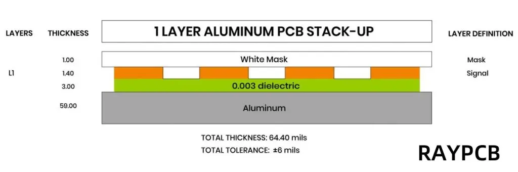
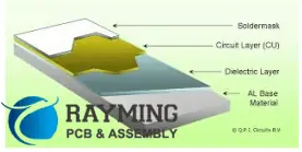
An Aluminum PCB Stackup refers to the layered construction of a printed circuit board that incorporates an aluminum base layer. This structure typically consists of three main components:

  1. Metal Base Layer (Aluminum Core): This forms the foundation of the PCB, providing mechanical support and excellent thermal conductivity.
  2. Dielectric Insulating Layer: A thin layer of thermally conductive yet electrically insulating material that separates the aluminum core from the copper circuitry.
  3. Copper Circuitry Layer: The topmost layer where electronic components are mounted and interconnected.

Comparison to Traditional FR4 Stackups

Unlike traditional FR4 (Flame Retardant 4) stackups that use a fiberglass-reinforced epoxy laminate as the base material, Aluminum PCB Stackups leverage the superior thermal properties of aluminum. This fundamental difference results in significantly improved heat dissipation capabilities, making Aluminum PCB Stackups ideal for high-power applications.

Key Benefits of Aluminum PCB Stackups

Superior Thermal Conductivity

The standout feature of Aluminum PCB Stackups is their exceptional thermal conductivity. The aluminum core acts as a built-in heat sink, efficiently spreading and dissipating heat generated by electronic components. This property is particularly valuable in applications where thermal management is critical, such as high-power LED lighting or automotive electronics.

Enhanced Mechanical Durability

Aluminum’s inherent strength and rigidity contribute to the overall durability of the PCB. This increased mechanical stability helps protect sensitive components from vibration and physical stress, making Aluminum PCB Stackups well-suited for rugged environments.

Lightweight and Compact Design

Despite its strength, aluminum is relatively lightweight compared to other metals. This characteristic allows for the creation of robust yet lightweight PCBs, which is particularly advantageous in applications where weight is a concern, such as aerospace or portable electronics.

Cost-effectiveness for High-Power Applications

While the initial cost of Aluminum PCB Stackups may be higher than traditional FR4 boards, they often prove more cost-effective in high-power applications. The improved thermal management can reduce or eliminate the need for additional cooling solutions, potentially lowering overall system costs.

Challenges in Designing an Aluminum PCB Stackup

Managing Differential Thermal Expansion

One of the primary challenges in designing Aluminum PCB Stackups is managing the differential thermal expansion between the aluminum core and other materials in the stackup. As temperature fluctuates, materials expand and contract at different rates, which can lead to stress and potential delamination if not properly addressed.

Maintaining Signal Integrity at High Frequencies

While Aluminum PCB Stackups excel in thermal management, they present unique challenges for signal integrity, especially at high frequencies. The proximity of the conductive aluminum layer to the signal traces can affect impedance and introduce unwanted capacitance, requiring careful design considerations.

Layer Adhesion and Material Compatibility

Ensuring strong adhesion between the aluminum core, dielectric layer, and copper circuitry is crucial for the longevity and reliability of the PCB. Selecting compatible materials and employing appropriate manufacturing processes are essential to prevent delamination and ensure the PCB’s long-term performance.

Thermal Conductivity Considerations

Role of the Dielectric Layer’s Thermal Conductivity

The dielectric layer plays a crucial role in the thermal performance of an Aluminum PCB Stackup. While it must provide electrical isolation, it should also facilitate heat transfer from the copper layer to the aluminum core. Selecting a dielectric material with high thermal conductivity is key to maximizing the stackup’s heat dissipation capabilities.

Thickness of the Aluminum Core and Heat Dissipation

The thickness of the aluminum core directly impacts the PCB’s ability to spread and dissipate heat. A thicker core generally provides better thermal performance but comes at the cost of increased weight and potentially higher manufacturing complexity. Designers must carefully balance these factors based on the specific requirements of their application.

Examples: Applications in LED Lighting, Automotive, and Power Electronics

Aluminum PCB Stackups find extensive use in applications requiring efficient thermal management:

  1. LED Lighting: High-power LED modules benefit from the enhanced heat dissipation, allowing for brighter and more reliable lighting solutions.
  2. Automotive Electronics: Under-hood electronics and LED headlights leverage Aluminum PCB Stackups to withstand high temperatures and vibrations.
  3. Power Electronics: Inverters, motor drives, and power supplies use Aluminum PCB Stackups to manage the heat generated by high-current components.

Read more about:

Signal Integrity Factors in Aluminum PCB Stackups

Importance of Consistent Impedance Control

Maintaining consistent impedance throughout the PCB is crucial for signal integrity, especially in high-speed digital and RF applications. The presence of the aluminum layer can affect impedance characteristics, requiring careful design and potentially the use of impedance-controlled dielectric materials.

Effects of the Dielectric Constant on Signal Propagation

The dielectric constant of the insulating layer influences signal propagation speed and can impact timing in high-speed circuits. Designers must consider this factor when selecting materials and determining trace geometries to ensure proper signal timing and minimize reflections.

Mitigating Signal Loss and Cross-talk in Multilayer Aluminum PCBs

As with traditional PCBs, multilayer Aluminum PCB Stackups must address signal loss and cross-talk issues. The proximity of the aluminum layer can exacerbate these problems, necessitating careful layer stackup planning, appropriate use of ground planes, and strategic trace routing to maintain signal integrity.

Common Aluminum PCB Stackup Configurations

Aluminum PCB LAYER
Aluminum PCB LAYER

Single-sided Aluminum PCB Stackup

The simplest configuration consists of an aluminum base, a dielectric layer, and a single copper layer for circuitry. This design is cost-effective and suitable for applications with straightforward thermal requirements and low complexity.

Double-sided Aluminum PCB Stackup

This configuration adds a second copper layer on the opposite side of the aluminum core, separated by another dielectric layer. It offers increased routing flexibility and can accommodate more complex circuits while maintaining excellent thermal properties.

Multilayer Aluminum PCB Designs

For applications requiring higher complexity, multilayer Aluminum PCB Stackups can be created. These designs typically involve additional dielectric and copper layers built up on one or both sides of the aluminum core. Careful consideration must be given to thermal vias and layer arrangement to maintain optimal heat dissipation.

Hybrid Structures: Combining FR4 and Aluminum Layers

Some designs benefit from a hybrid approach, combining the thermal advantages of aluminum with the cost-effectiveness and familiarity of FR4. These stackups might feature an aluminum core with FR4 layers built up on one or both sides, offering a balance between thermal performance and traditional PCB design techniques.

Material Selection for Optimal Performance

Choosing the Right Dielectric Material

Selecting the appropriate dielectric material is crucial for balancing thermal conductivity and signal integrity. Materials like ceramic-filled epoxy offer high thermal conductivity but may have higher dielectric constants, affecting signal propagation. Conversely, materials with lower dielectric constants might not provide optimal thermal performance.

Copper Thickness Considerations

The thickness of the copper layers affects both electrical and thermal performance. Thicker copper can carry higher currents and aid in heat spreading but may complicate fine-pitch routing and impedance control. Designers must balance these factors based on their specific application requirements.

Aluminum Alloy Types and Their Impact

Different aluminum alloys offer varying thermal, mechanical, and cost characteristics. Common choices include Alloy 1050A for general applications and Alloy 6061 for improved strength. The selection of aluminum alloy can impact the overall performance and cost of the Aluminum PCB Stackup.

Best Practices for Designing an Effective Aluminum PCB Stackup

Aluminum PCB Properties

Thermal Simulation During Design

Utilizing thermal simulation tools during the design phase is crucial for optimizing heat dissipation. These simulations can help identify hotspots, validate cooling strategies, and ensure that the Aluminum PCB Stackup meets the thermal requirements of the application.

Via Design and Thermal Vias

Strategic placement of vias, especially thermal vias, is essential for efficient heat transfer in multilayer designs. Thermal vias provide direct paths for heat to travel from outer layers to the aluminum core, improving overall thermal performance.

Balancing Cost, Performance, and Manufacturability

While Aluminum PCB Stackups offer superior thermal performance, they can be more expensive and challenging to manufacture than traditional PCBs. Designers must carefully balance these factors, considering the entire system cost and performance requirements when deciding on the optimal stackup configuration.

Applications of Aluminum PCB Stackups

High-power LED Modules

Aluminum PCB Stackups are widely used in high-power LED applications, from street lighting to automotive headlights. The efficient heat dissipation allows for higher LED density and brightness while ensuring long-term reliability.

Automotive Electronics

The automotive industry leverages Aluminum PCB Stackups for various applications, including engine control units, LED lighting, and power converters. The combination of thermal management and mechanical durability makes them ideal for the harsh automotive environment.

Industrial Power Equipment

Industrial motor drives, inverters, and power supplies benefit from the high current-carrying capacity and thermal performance of Aluminum PCB Stackups. These attributes enable more compact and efficient power electronics designs.

RF and Microwave Devices

Despite the challenges in maintaining signal integrity, carefully designed Aluminum PCB Stackups find use in RF and microwave applications. The thermal benefits can outweigh the design complexities in high-power RF amplifiers and transmitters.

Future Trends in Aluminum PCB Stackups

Advances in Dielectric Materials

Ongoing research into advanced dielectric materials promises to further improve the thermal and electrical performance of Aluminum PCB Stackups. Materials with higher thermal conductivity and lower dielectric constants will enable even more efficient designs.

Innovations in Multilayer Aluminum Stackups

As demand for higher complexity circuits with excellent thermal management grows, we can expect innovations in multilayer Aluminum PCB Stackup designs. This may include novel layer arrangements and improved manufacturing techniques to optimize both thermal and electrical performance.

Integration with Flexible and Hybrid PCB Technologies

The future may see increased integration of Aluminum PCB Stackups with flexible and rigid-flex technologies, combining the thermal benefits of aluminum with the versatility of flexible circuits. This could open up new possibilities in wearable electronics and other applications requiring both flexibility and thermal management.

Conclusion

Aluminum PCB Stackups represent a significant advancement in PCB technology, offering a powerful solution to the dual challenges of thermal management and signal integrity. By leveraging the superior thermal properties of aluminum while carefully addressing the unique design considerations, engineers can create high-performance PCBs capable of meeting the demands of modern electronics.

As we’ve explored throughout this article, the key to success with Aluminum PCB Stackups lies in understanding their unique characteristics and applying best practices in design and material selection. Whether it’s for high-power LEDs, automotive electronics, or cutting-edge RF devices, a well-designed Aluminum PCB Stackup can provide the perfect balance of thermal conductivity and reliable signal performance.

As technology continues to advance, we can expect further innovations in Aluminum PCB Stackup designs, materials, and manufacturing processes. These developments will undoubtedly expand the applications and capabilities of this versatile technology, solidifying its place as a cornerstone of modern electronic design.

FAQs about Aluminum PCB Stackup

  1. What makes Aluminum PCB Stackups different from standard PCBs? Aluminum PCB Stackups feature an aluminum core that provides superior thermal conductivity compared to traditional FR4 PCBs. This makes them ideal for applications requiring efficient heat dissipation.
  2. Can multilayer Aluminum PCBs maintain high signal integrity? Yes, with careful design considerations. While the aluminum layer can affect signal propagation, proper stackup planning, material selection, and layout techniques can ensure high signal integrity in multilayer designs.
  3. How does the aluminum core thickness affect PCB performance? A thicker aluminum core generally improves thermal performance by providing better heat spreading. However, it also increases weight and can affect manufacturing complexity, so the thickness must be balanced with other design requirements.
  4. Are Aluminum PCB Stackups suitable for all types of electronic designs? While Aluminum PCB Stackups excel in high-power and thermally demanding applications, they may not be necessary or cost-effective for all designs. They are most beneficial in scenarios where thermal management is a critical concern.
  5. How do you address the differential thermal expansion in Aluminum PCB Stackups? Careful material selection, appropriate layer thicknesses, and strategic use of vias can help manage differential thermal expansion. Some designs may also incorporate stress-relief features to minimize the impact of thermal cycling.

KiCad’s ODB++ Export: Bridging the Gap Between Design and PCB Manufacturing

In the world of Printed Circuit Board (PCB) design and manufacturing, seamless communication between designers and fabricators is crucial. As the complexity of electronic designs increases, so does the need for more comprehensive and error-free data formats. Enter KiCad’s ODB++ export functionality โ€“ a game-changing feature that’s revolutionizing how open-source PCB designs transition from concept to reality. This article delves into the intricacies of KiCad’s ODB++ export, exploring its significance in modern PCB manufacturing workflows and how it’s bridging the gap between design and production.

YouTube video

Introduction

The journey from a PCB design to a physical board involves multiple steps, each critical to the final product’s quality and functionality. Traditionally, this process relied heavily on Gerber files โ€“ a long-standing industry standard for communicating PCB design data. However, as designs grow more complex, the limitations of Gerber files become increasingly apparent.

KiCad, a popular open-source electronic design automation (EDA) software, has been at the forefront of addressing these challenges. With its recent introduction of ODB++ export capabilities, KiCad is not just keeping pace with industry trends โ€“ it’s setting new standards for open-source PCB design tools.

This article aims to explore how KiCad’s ODB++ export enhances the PCB manufacturing process, offering insights into its implementation, benefits, and best practices for designers and manufacturers alike.

What is ODB++?

Definition and History

ODB++ (Open Database++) is a proprietary PCB manufacturing data exchange format developed by Valor Computerized Systems, now part of Siemens Digital Industries Software. Introduced in the 1990s, ODB++ was designed to address the limitations of traditional Gerber files by providing a more comprehensive and intelligent data format for PCB manufacturing.

Why ODB++ Matters

Unlike traditional Gerber files, which primarily contain 2D image data of PCB layers, ODB++ offers a richer, more complete representation of the PCB design. This comprehensive approach includes:

  1. Layer information
  2. Netlist data
  3. Component placement
  4. Manufacturing notes
  5. Material specifications

The result is a single, cohesive package that contains all the information needed to manufacture a PCB, reducing the chances of misinterpretation or data loss between design and production stages.

Key Benefits of ODB++ in PCB Manufacturing

  1. Fewer Errors: By providing a more complete dataset, ODB++ reduces the likelihood of miscommunication or missing information, leading to fewer manufacturing errors.
  2. Easier CAM Processing: Computer-Aided Manufacturing (CAM) systems can directly interpret ODB++ data, streamlining the pre-production process and reducing manual intervention.
  3. Improved Communication: ODB++ facilitates clearer communication between designers and manufacturers, as all relevant information is contained in a single, standardized format.
  4. Time and Cost Savings: With reduced errors and streamlined processes, ODB++ can lead to faster turnaround times and lower overall production costs.

KiCad’s Evolution Toward Professional Manufacturing Support

Background on KiCad’s Capabilities

KiCad has long been a favorite among hobbyists and professionals alike for its powerful, free, and open-source approach to PCB design. Historically, KiCad has supported standard output formats like Gerber and Excellon drill files, which have been the industry norm for decades.

Challenges with Traditional Gerber + Drill Files

While Gerber files have served the industry well, they come with limitations:

  1. Multiple Files: A complete Gerber package typically includes separate files for each PCB layer, drill data, and often additional documentation.
  2. Limited Intelligence: Gerber files essentially describe PCB layers as images, lacking inherent information about connectivity or component properties.
  3. Potential for Errors: Managing multiple files increases the risk of missing or mismatched data during the handoff to manufacturers.

Growing Demand for ODB++ in Open-Source Workflows

As more professional designers and manufacturers adopt open-source tools like KiCad, the demand for industry-standard outputs like ODB++ has grown. This push reflects a broader trend in the industry towards more integrated, data-rich design-to-manufacturing workflows.

KiCad’s ODB++ Implementation

KiCad introduced ODB++ export capabilities in version 6.0, with continued improvements in subsequent releases. This addition marked a significant step in KiCad’s evolution, aligning it more closely with commercial EDA tools and professional manufacturing requirements.

Read more about:

How KiCad Exports ODB++

Step-by-Step Guide to ODB++ Export in KiCad

  1. Open Your PCB Project: Ensure your design is finalized and ready for manufacturing.
  2. Access the Export Menu:
    • Navigate to “File” > “Export” > “ODB++”
    • Alternatively, use the shortcut Ctrl+Alt+O (Windows/Linux) or Cmd+Alt+O (Mac)
  3. Configure Export Settings:
    • Choose the output directory
    • Select layers to include
    • Specify netlist and drill file options
  4. Review and Confirm: Double-check your settings before initiating the export process.
  5. Export: Click “Export” to generate the ODB++ files.

Overview of Export Options and Settings

  • Layers: Select which PCB layers to include in the ODB++ output.
  • Netlist: Choose to include detailed netlist information.
  • Drill Files: Specify drill file formats and options.
  • Component Placement: Include data on component positions and orientations.
  • Design Rules: Option to include DRC (Design Rule Check) information.

Practical Tips for Clean ODB++ Export

  1. Validate Your Design: Run DRC checks before exporting to ensure your design is error-free.
  2. Use Consistent Units: Ensure all measurements in your design use consistent units to avoid conversion issues.
  3. Check Layer Stack-up: Verify that your layer stack-up is correctly defined before export.
  4. Review Component Properties: Ensure all components have correct footprints and attributes assigned.

Common Mistakes to Avoid

  1. Incomplete Layer Selection: Forgetting to include critical layers in the export.
  2. Ignoring DRC Errors: Exporting without resolving design rule violations.
  3. Outdated Libraries: Using old component libraries that may not align with current manufacturing standards.
  4. Neglecting Mechanical Layers: Forgetting to include important mechanical information like board outlines or assembly notes.

Why Use ODB++ with KiCad?

ODB++ Vs. Gerber
ODB++ Vs. Gerber

Advantages over Traditional Gerber Exports

  1. Consolidated Package: ODB++ provides all necessary manufacturing data in a single, organized structure, reducing the risk of missing files.
  2. Enhanced Data Intelligence: ODB++ includes detailed information about components, nets, and design rules, enabling more intelligent processing by manufacturers.
  3. Improved Accuracy: The comprehensive nature of ODB++ data reduces the chance of misinterpretation or errors during the manufacturing process.
  4. Faster Turnaround: With more complete data upfront, manufacturers can often process ODB++ files more quickly, potentially leading to faster production times.

Better Error Checking and Validation

ODB++ allows for more thorough automated checks at the manufacturing stage, catching potential issues that might be missed with Gerber files alone. This can include:

Reduced Back-and-Forth with PCB Fabricators

The comprehensive nature of ODB++ often results in fewer queries from manufacturers, streamlining the production process. This reduction in communication cycles can lead to:

  • Faster time-to-market
  • Fewer opportunities for miscommunication
  • Reduced overall project stress

Real-World Feedback from Manufacturers

Many PCB manufacturers report preferring ODB++ files for several reasons:

  1. Ease of Use: ODB++ files are often easier to import and process in modern CAM systems.
  2. Reduced Pre-Production Time: The completeness of ODB++ data often results in less time spent on pre-production setup and checks.
  3. Higher Confidence: Manufacturers often express higher confidence in the accuracy of ODB++ data compared to traditional Gerber files.

Limitations and Considerations

ODB++ Export Maturity in KiCad

While KiCad’s ODB++ export functionality is a significant advancement, it’s important to note that it’s still a relatively new feature. As with any software feature, there may be occasional bugs or limitations:

  1. Ongoing Development: The KiCad team continues to refine and improve ODB++ export capabilities with each release.
  2. Community Feedback: Users are encouraged to report any issues or inconsistencies they encounter to help improve the feature.
  3. Version Compatibility: Always check the KiCad release notes for the latest information on ODB++ export capabilities and any known issues.

Compatibility Considerations

While ODB++ is growing in popularity, it’s not universally accepted by all PCB manufacturers:

  1. Check with Your Manufacturer: Always verify that your chosen PCB fabricator accepts and can process ODB++ files.
  2. Gerber as Backup: Consider providing both ODB++ and traditional Gerber files to ensure compatibility with a wider range of manufacturers.
  3. Growing Acceptance: More PCB fabricators are adding ODB++ support, but it’s not yet universal.

When to Stick with Traditional Outputs

There are scenarios where traditional Gerber files might still be preferable:

  1. Simple Designs: For very simple PCBs, the additional complexity of ODB++ might not offer significant advantages.
  2. Manufacturer Preference: Some PCB fabricators might still prefer or only accept Gerber files.
  3. Legacy Systems: If you’re working with older manufacturing systems or processes, Gerber files might be more compatible.

Best Practices for Smooth Handoff to PCB Manufacturers

Checklist for Validating ODB++ Files Before Sending

  1. Layer Completeness: Ensure all necessary layers are included in the ODB++ package.
  2. Netlist Verification: Double-check that the netlist in the ODB++ file matches your design intent.
  3. Component Placement: Verify that all components are correctly placed and oriented.
  4. Drill File Accuracy: Confirm that all drill data is accurate and complete.
  5. Design Rule Compliance: Run a final DRC check to ensure all design rules are met.

Recommended Tools for Previewing ODB++ Outputs

  1. ODB++ Viewer: Use specialized ODB++ viewing software to inspect your export.
  2. CAM350: A professional tool that can open and analyze ODB++ files.
  3. CircuitCAM: Another professional option for viewing and validating ODB++ data.
  4. Online Viewers: Some PCB manufacturers offer online tools to preview and check ODB++ files before submission.

Communicating with Your PCB Fab About ODB++ Capabilities

  1. Early Inquiry: Reach out to your manufacturer early in the design process to discuss their ODB++ capabilities.
  2. Specification Alignment: Ensure your ODB++ export settings align with your manufacturer’s requirements.
  3. Version Information: Provide information about the KiCad version used for the export, as this can be helpful for troubleshooting.
  4. Feedback Loop: Establish a clear channel for feedback from the manufacturer regarding the ODB++ files.

Conclusion

KiCad’s support for ODB++ export represents a significant leap forward in bridging the gap between open-source PCB design and professional manufacturing processes. By providing a more comprehensive and intelligent data format, KiCad is empowering designers to communicate their intentions more clearly and efficiently with manufacturers.

The introduction of ODB++ export in KiCad not only enhances the software’s capabilities but also elevates the entire open-source PCB design ecosystem. It demonstrates that open-source tools can indeed meet and even exceed industry standards, providing professionals with powerful, cost-effective alternatives to proprietary solutions.

As KiCad continues to evolve and refine its ODB++ export functionality, designers are encouraged to explore this feature alongside traditional Gerber exports. The potential benefits in terms of reduced errors, faster turnaround times, and improved communication with manufacturers make it a valuable addition to any PCB designer’s toolkit.

The ongoing development and improvement of features like ODB++ export in KiCad underscore the software’s commitment to providing cutting-edge, professional-grade tools to the open-source community. As more designers adopt these advanced features and provide feedback, we can expect to see even greater strides in the capabilities and reliability of open-source PCB design tools.

In embracing ODB++ export with KiCad, designers are not just improving their own workflows โ€“ they’re contributing to a broader shift in the industry towards more open, efficient, and collaborative PCB design and manufacturing processes.

Additional Resources

FAQ

Does KiCad support ODB++?

Yes, KiCad supports ODB++ export starting from version 6.0, with ongoing improvements in subsequent releases.

What’s the difference between ODB++ and Gerber in KiCad?

While Gerber files primarily contain 2D image data of PCB layers, ODB++ provides a more comprehensive package including netlist data, component placement, and manufacturing notes, all in a single, structured format.

Can you edit ODB++ files exported from KiCad?

ODB++ files are not directly editable like Gerber files. They’re intended as a final output for manufacturing. Any changes should be made in the original KiCad design and then re-exported.

What is a Gerber File? The Essential Guide for PCB Design and Manufacturing

Introduction

In the world of Printed Circuit Board (PCB) design and manufacturing, few elements are as crucial as the Gerber file. These unassuming files serve as the bridge between the intricate designs crafted by engineers and the physical boards that power our electronic devices. But what exactly is a Gerber file, and why is it so vital to the PCB production process?

Gerber files are the industry standard for transmitting PCB design data to manufacturers. They contain all the necessary information for creating each layer of a PCB, from copper traces to solder mask and silkscreen. Without accurate Gerber files, even the most brilliantly designed circuit board would be impossible to produce correctly.

YouTube video

For PCB designers and manufacturers alike, a thorough understanding of Gerber files is not just beneficialโ€”it’s essential. Mastering the intricacies of Gerber files can mean the difference between a smooth production run and costly errors that require multiple revisions. Whether you’re a seasoned engineer or new to the field of PCB design, grasping the fundamentals of Gerber files will enhance your ability to create high-quality, manufacturable designs.

In this comprehensive guide, we’ll delve deep into the world of Gerber files. We’ll explore their origins, examine their structure, and uncover best practices for creating and handling these critical PCB design files. By the end of this article, you’ll have a solid foundation in Gerber file knowledge, empowering you to navigate the PCB design and manufacturing process with confidence.

1. What is a Gerber File?

Definition and Purpose

A Gerber file is a standardized vector format used in the electronics industry to describe the layers of a printed circuit board (PCB). It contains information about various PCB elements, including copper traces, solder mask, silkscreen, and drill holes. Essentially, Gerber files serve as a universal language between PCB designers and manufacturers, ensuring that the final product matches the intended design precisely.

A Brief History

The Gerber file format has its roots in the early days of PCB manufacturing. It was developed in the 1960s by Gerber Systems Corporation, founded by H. Joseph Gerber. Initially, these files were used to control vector photoplotters, machines that exposed photoresist-coated materials to light, creating the artwork for PCB production.

Over time, as PCB design became increasingly complex, the Gerber format evolved. The original standard, known as RS-274D, was eventually superseded by the more capable RS-274X format. This newer version, sometimes called “Extended Gerber,” includes additional features that make it more suitable for modern PCB designs.

Industry Standards: RS-274D vs RS-274X

While both RS-274D and RS-274X are referred to as “Gerber” formats, there are significant differences between them:

  1. RS-274D (Standard Gerber):
    • Older format
    • Requires separate aperture definition files
    • Limited in its ability to define complex shapes
  2. RS-274X (Extended Gerber):
    • Modern standard
    • Includes aperture definitions within the file
    • Supports more complex shapes and features
    • More efficient and less prone to errors

Today, RS-274X is the preferred format for most PCB manufacturers due to its enhanced capabilities and reduced potential for misinterpretation.

The Role of Gerber Files in PCB Production

Gerber files play a crucial role in translating PCB designs into physical boards. They act as a set of instructions for manufacturing equipment, guiding processes such as:

  1. Photoplotter imaging
  2. CNC drilling
  3. Solder mask application
  4. Silkscreen printing

By providing precise, layer-by-layer information, Gerber files ensure that every aspect of the PCB design is accurately reproduced during manufacturing. This level of detail is essential for creating functional, high-quality circuit boards that meet the exacting standards of modern electronics.

Read more about:

2. Why Are Gerber Files Important for PCB Manufacturing?

The Cornerstone of PCB Fabrication

Gerber files are the lifeblood of PCB manufacturing. They serve as the primary means of communication between designers and fabricators, ensuring that the final product matches the intended design with utmost precision. Here’s why Gerber files are so crucial:

  1. Universal Language: Gerber files provide a standardized format that can be understood by various manufacturing equipment and software, regardless of the original design tool used.
  2. Layered Information: They contain separate data for each layer of the PCB, allowing manufacturers to create complex, multi-layer boards accurately.
  3. Precision: Gerber files offer high-resolution data, enabling the creation of intricate designs with fine details.

How Manufacturers Use Gerber Files

PCB manufacturers rely on Gerber files to guide every step of the fabrication process. Here’s how different Gerber file layers are used:

  1. Copper Layers: These files guide the etching process to create the conductive traces on the PCB.
  2. Solder Mask Layers: Determine where the protective solder mask should be applied or removed.
  3. Silkscreen Layers: Guide the application of component labels, logos, and other printed information on the board.
  4. Drill Files: While technically not Gerber files (usually in Excellon format), these accompany Gerber files to specify the location and size of holes and vias.

Risks of Incorrect Gerber Files

The importance of accurate Gerber files cannot be overstated. Errors in these files can lead to significant issues:

  1. Production Errors: Inaccurate Gerber files can result in misplaced components, incorrect trace widths, or missing features on the final PCB.
  2. Costly Revisions: Mistakes discovered after production require new boards to be manufactured, leading to increased costs and delays.
  3. Functionality Issues: Errors in Gerber files can create PCBs that fail to function as intended, potentially causing problems in the final product.
  4. Wasted Materials: Incorrect files may lead to scrapped boards, wasting valuable materials and resources.

By understanding the critical role of Gerber files in PCB manufacturing, designers can better appreciate the need for accuracy and attention to detail when preparing these files for production.

3. Components and Layers in a Gerber File

Different software have different method to generate Gerber,EAGLE

Understanding PCB Layers

A typical PCB consists of multiple layers, each serving a specific purpose in the board’s functionality. Gerber files provide detailed information for each of these layers, ensuring that the PCB is manufactured exactly as designed. Let’s explore the common layers included in a set of Gerber files:

1. Copper Layers

Copper layers are the heart of any PCB, carrying the electrical signals between components. A typical set of Gerber files includes:

  • Top Copper Layer: Contains the copper traces and pads on the top side of the board.
  • Bottom Copper Layer: Represents the copper traces and pads on the bottom side.
  • Inner Copper Layers: For multi-layer boards, additional copper layers are sandwiched between the top and bottom layers.

2. Solder Mask Layers

Solder mask is a thin lacquer-like layer of polymer that is usually applied to the copper layers of a PCB to protect the copper from oxidation and to prevent solder bridges from forming between closely spaced solder pads. Gerber files for solder mask typically include:

  • Top Solder Mask: Defines areas on the top of the board where solder mask should be applied or removed.
  • Bottom Solder Mask: Specifies solder mask application for the bottom of the board.

3. Silkscreen Layers

Silkscreen layers contain text and symbols printed on the PCB surface, providing valuable information for assembly and future reference. These layers usually include:

  • Top Silkscreen: Text and symbols to be printed on the top side of the board.
  • Bottom Silkscreen: Text and symbols for the bottom side of the board.

4. Drill Files

While not technically Gerber files, drill files are crucial companions to the Gerber set. They specify the location, size, and type of all holes in the PCB. Drill files are typically in Excellon format and include:

  • Plated Holes: For component leads and vias.
  • Non-Plated Holes: For mounting or other mechanical purposes.

5. Board Outline

The board outline file defines the physical shape and dimensions of the PCB. It’s crucial for ensuring that the board fits properly into its intended housing or alongside other components.

Example of a Full Set of Gerber Files

A complete set of Gerber files for a typical two-layer PCB might include:

  1. TopCopper.gbr
  2. BottomCopper.gbr
  3. TopSolderMask.gbr
  4. BottomSolderMask.gbr
  5. TopSilkscreen.gbr
  6. BottomSilkscreen.gbr
  7. BoardOutline.gbr
  8. Drill.xln (Excellon drill file)

For more complex multi-layer boards, additional layers would be included, such as Inner1Copper.gbr, Inner2Copper.gbr, etc.

Understanding the components and layers in a Gerber file set is crucial for both PCB designers and manufacturers. It ensures that all necessary information is included and properly organized, leading to accurate and efficient PCB production.

4. How to Generate a Gerber File from PCB Design Software

PCB Design Software Altium Designer

Creating accurate Gerber files is a critical step in the PCB design process. Most modern PCB design software packages include built-in tools for generating Gerber files. While the exact process may vary between different software, the general principles remain the same. Let’s look at how to generate Gerber files using some popular PCB design tools:

Altium Designer

  1. Open your PCB project in Altium Designer.
  2. Go to “File” > “Fabrication Outputs” > “Gerber Files”.
  3. In the Gerber setup dialog, ensure all necessary layers are selected.
  4. Set the output directory and other parameters as needed.
  5. Click “OK” to generate the Gerber files.

KiCad

  1. Open your PCB layout in KiCad’s PCB Editor.
  2. Go to “File” > “Plot”.
  3. In the Plot dialog, select the layers you want to export.
  4. Choose your output directory and format (typically, use “Gerber” format).
  5. Click “Plot” to generate the files.
  6. For drill files, use the “Generate Drill Files” button in the same dialog.

Eagle

  1. Open your board layout in Eagle.
  2. Go to “File” > “CAM Processor”.
  3. In the CAM Processor, select a suitable job file (e.g., “gerb274x.cam” for extended Gerber).
  4. Verify that all necessary layers are included.
  5. Click “Process Job” to generate the Gerber files.

EasyEDA

  1. Open your PCB design in EasyEDA.
  2. Click on the “Fabrication” button in the top toolbar.
  3. In the Fabrication Output dialog, ensure “Gerber” is selected.
  4. Choose your layer setup and other parameters.
  5. Click “Generate Gerber” to create the files.

Common Export Settings to Check

Regardless of the software you’re using, there are several important settings to verify when generating Gerber files:

  1. Units: Ensure the correct unit (inches or millimeters) is selected.
  2. Format: Choose the appropriate Gerber format (typically RS-274X for modern designs).
  3. Layers: Verify that all necessary layers are included in the export.
  4. Precision: Set the coordinate precision (usually 2:4 or 2:5 for inches, 3:3 or 4:4 for millimeters).
  5. Apertures: For older formats, ensure apertures are correctly defined.
  6. Drill File Format: Typically, use Excellon format for drill files.

By carefully checking these settings and following the correct procedures for your specific PCB design software, you can ensure that your Gerber files accurately represent your PCB design and are ready for manufacturing.

5. Best Practices for Preparing and Checking Gerber Files

Preparing and verifying Gerber files is a crucial step in ensuring successful PCB manufacturing. Following best practices can help you avoid costly errors and delays. Here are some key strategies to implement:

Importance of Design Rule Checks (DRC)

Before exporting Gerber files, it’s essential to run a thorough Design Rule Check (DRC) in your PCB design software. DRC helps identify potential issues such as:

  1. Trace width and spacing violations
  2. Clearance errors
  3. Unconnected nets
  4. Drill and pad size mismatches

Resolving these issues before generating Gerber files can prevent many common manufacturing problems.

Using Gerber Viewers for Verification

After generating Gerber files, it’s crucial to verify them using specialized Gerber viewer software. This step allows you to visually inspect your design and catch any issues that might have been missed. Popular Gerber viewers include:

  1. Gerbv: An open-source Gerber viewer for Linux, macOS, and Windows.
  2. ViewMate: A free Gerber viewer from PentaLogix.
  3. GerberLogix: A comprehensive Gerber file viewer and editor.

When using a Gerber viewer:

  1. Load all layers and check their alignment.
  2. Verify that all expected features are present.
  3. Check for any unexpected artifacts or missing elements.
  4. Confirm that drill holes are correctly placed.

Common Mistakes to Avoid

When preparing Gerber files, be aware of these frequent pitfalls:

  1. Missing Layers: Ensure all necessary layers (copper, solder mask, silkscreen, etc.) are included in your Gerber set.
  2. Incorrect Layer Polarity: Verify that positive and negative layers are correctly defined, especially for solder mask and silkscreen.
  3. Mismatched Units: Ensure consistency in units (inches or millimeters) across all files.
  4. Outdated Design Elements: Remove any unused or outdated elements from your design before generating Gerber files.
  5. Incompatible Drill File Format: Make sure your drill file format is compatible with your manufacturer’s requirements.
  6. Inaccurate Board Outline: Verify that the board outline is correctly defined and matches your design intentions.
  7. Insufficient Precision: Use appropriate numerical precision in your Gerber files to ensure accurate representation of your design.

Additional Best Practices

  1. Use Descriptive Filenames: Name your Gerber files clearly and consistently (e.g., ProjectName_TopCopper.gbr).
  2. Include a README File: Provide a text file explaining the contents of your Gerber package, including any special instructions.
  3. Double-Check Drill Files: Ensure that your drill files accurately represent all holes in your design.
  4. Verify Against Manufacturing Guidelines: Check your design against your chosen manufacturer’s specific guidelines and capabilities.
  5. Use Panelization Carefully: If panelizing your design, ensure that the panel layout is correct and includes necessary features like fiducials and breakaway tabs.

By following these best practices and carefully checking your Gerber files before submission, you can significantly reduce the risk of manufacturing errors and ensure a smoother PCB production process.

6. How to Submit Gerber Files to PCB Manufacturers

Submitting Gerber files to PCB manufacturers is the final step in bringing your design to life. Proper submission ensures that your design is interpreted correctly and manufactured efficiently. Here’s a guide to help you through this crucial process:

Zipping and Naming Gerber Files

  1. Create a Zip Archive: Compress all your Gerber files and associated documents into a single ZIP file. This makes it easier to upload and keeps all files together.
  2. Use Clear, Consistent Naming: Name your ZIP file clearly, including the project name and version number (e.g., “ProjectName_v1.0_Gerbers.zip”).
  3. Organize Internal Folders: If your Gerber set is complex, consider organizing files into subfolders within the ZIP (e.g., “Gerbers”, “Drills”, “Documentation”).

Manufacturer-Specific Requirements

Different PCB manufacturers may have specific requirements for Gerber file submissions. Always check with your chosen manufacturer for their particular guidelines. Common requirements include:

  • File Format Versions: Confirm which Gerber format (e.g., RS-274X) and drill file format (e.g., Excellon) the manufacturer prefers.
  • Layer Naming Conventions: Some manufacturers have specific naming conventions for Gerber files (e.g., GTL for top copper, GBL for bottom copper).
  • Additional Documentation: Many manufacturers require a fabrication drawing or assembly drawing along with the Gerber files.
  • Board Specifications: Provide details such as board thickness, copper weight, and material type in a separate document.

Example of a Submission Checklist

To ensure you’ve covered all bases, use a checklist like this when submitting your Gerber files:

  1. Gerber files for all PCB layers (copper, solder mask, silkscreen, etc.)
  2. Drill file (Excellon format)
  3. Board outline file
  4. Fabrication drawing (if required)
  5. Bill of Materials (BOM) for assembly orders
  6. Pick and place file for assembly orders
  7. README file with any special instructions or notes
  8. Confirmation that all files use consistent units (inches or mm)
  9. Verification that file naming follows manufacturer’s conventions
  10. Check that the Gerber format matches manufacturer’s requirements

Tips for a Smooth Submission Process

  1. Use the Manufacturer’s Online Platform: Many PCB manufacturers offer online portals for file submission, which often include automatic design rule checks.
  2. Communicate Special Requirements: If your design has any unusual features or requirements, communicate these clearly to the manufacturer.
  3. Request a Design Review: Some manufacturers offer a design review service. Take advantage of this to catch any potential issues before production.
  4. Keep Versions Organized: If you need to submit revised files, clearly indicate the new version number and what changes were made.
  5. Backup Your Files: Always keep a backup of the submitted Gerber files for your records.

By following these guidelines and maintaining clear communication with your PCB manufacturer, you can significantly increase the chances of a successful and efficient production run.

7. Common Errors and How to Fix Them

Even with careful preparation, errors can occur in Gerber files. Recognizing and addressing these issues promptly can save time and resources. Here are some common Gerber file errors and how to fix them:

1. Misaligned Layers

Problem: Layers in the PCB design do not align correctly when viewed in a Gerber viewer.

Solution:

  • Check the origin point settings in your PCB design software.
  • Ensure all layers use the same coordinate system.
  • Re-export the Gerber files with corrected settings.

2. Missing Apertures

Problem: Certain features are missing or appear incomplete in the Gerber viewer.

Solution:

  • Verify that all necessary apertures are defined in your design.
  • Use the RS-274X format, which includes aperture definitions in the file.
  • Check your PCB design software’s export settings for aperture-related options.

3. Incorrect Board Outline

Problem: The board outline in the Gerber file doesn’t match the intended design.

Solution:

  • Ensure the board outline layer is correctly defined in your PCB design software.
  • Check that the board outline is a closed polygon without any gaps.
  • Verify that the board outline is included in the Gerber export process.

4. Drill File Mismatches

Problem: Drill holes don’t align with pads or are the wrong size.

Solution:

  • Confirm that the drill file uses the same unit and origin as the Gerber files.
  • Check for any scaling issues in the drill file export process.
  • Verify that hole sizes in the design match those in the drill file.

5. Layer Polarity Issues

Problem: Negative layers (like solder mask) appear positive or vice versa.

Solution:

  • Check the layer polarity settings in your PCB design software.
  • Verify that the Gerber file export process correctly handles layer polarities.
  • Use a Gerber viewer to confirm the correct appearance of each layer.

Tips for Troubleshooting

  1. Use Multiple Gerber Viewers: Different viewers may catch different issues.
  2. Compare with Original Design: Open your original PCB design alongside the Gerber files to spot discrepancies.
  3. Check Software Settings: Review your PCB design software’s export settings thoroughly.
  4. Consult with Manufacturers: Many PCB manufacturers offer design for manufacturing (DFM) checks that can catch common errors.
  5. Learn from Mistakes: Keep a log of errors encountered and their solutions for future reference.

By being aware of these common errors and knowing how to address them, you can improve the quality of your Gerber files and reduce the likelihood of manufacturing issues.

8. Future of Gerber Files in PCB Design

PCB Antenna Layout
PCB Antenna Layout

While Gerber files have been the industry standard for decades, the PCB design and manufacturing landscape is constantly evolving. Let’s explore the current trends and potential future of Gerber files in PCB design.

Introduction of New Formats

  1. ODB++: Developed by Mentor Graphics, ODB++ is a comprehensive data format that includes not just PCB layout data, but also component information and manufacturing instructions.
  2. IPC-2581: This open standard, developed by the IPC (Association Connecting Electronics Industries), aims to provide a single, unified data format for PCB manufacturing, assembly, and testing.

Will Gerber Files Still Dominate?

Despite the introduction of these new formats, Gerber files continue to be widely used due to several factors:

  1. Industry Inertia: Many manufacturers and designers are familiar with Gerber files and resistant to change.
  2. Proven Reliability: Gerber files have a long history of successful use in PCB manufacturing.
  3. Continuous Improvements: The Gerber format has evolved over time to meet new requirements, such as the introduction of the X2 format.
  4. Universal Support: Nearly all PCB design software and manufacturing equipment support Gerber files.

However, the limitations of Gerber files, such as the need for multiple files to represent a single board and lack of built-in component information, may gradually lead to increased adoption of newer formats.

Trends in Smart Manufacturing

The future of PCB design and manufacturing is likely to be influenced by broader trends in smart manufacturing:

  1. Increased Automation: More sophisticated data formats may be required to support fully automated manufacturing processes.
  2. Digital Twins: The concept of creating digital representations of physical products may drive the need for more comprehensive data formats.
  3. Industry 4.0: As factories become more connected and data-driven, there may be a push for more integrated design and manufacturing data formats.
  4. AI and Machine Learning: These technologies may be employed to optimize PCB designs and manufacturing processes, potentially requiring more detailed data than traditional Gerber files provide.

While Gerber files are likely to remain important in the near future, PCB designers and manufacturers should stay informed about emerging standards and be prepared to adapt to new technologies and data formats as they gain traction in the industry.

Conclusion

Gerber files remain the cornerstone of PCB design and manufacturing, serving as the critical link between designers’ visions and the physical reality of printed circuit boards. Throughout this guide, we’ve explored the intricacies of Gerber files, from their basic definition to best practices for their creation and use.

We’ve learned that Gerber files are more than just simple design files; they are a universal language in the PCB industry, enabling clear communication between designers and manufacturers. Their importance cannot be overstated, as accurate Gerber files are essential for producing high-quality, functional PCBs.

Key takeaways from this guide include:

  1. The structure and components of Gerber files, including various layers like copper, solder mask, and silkscreen.
  2. Best practices for generating Gerber files from popular PCB design software.
  3. The importance of thorough checking and verification of Gerber files before submission.
  4. Common errors in Gerber files and how to address them.
  5. The future of Gerber files in the context of evolving PCB design and manufacturing technologies.

As we look to the future, it’s clear that while new formats may emerge, Gerber files will continue to play a crucial role in PCB manufacturing for the foreseeable future. However, staying informed about new developments and being prepared to adapt to changing technologies will be crucial for PCB designers and manufacturers alike.

Remember, the key to successful PCB production lies in attention to detail and a thorough understanding of the Gerber file format. By mastering the creation and handling of Gerber files, you can ensure that your PCB designs are accurately translated from digital designs to physical boards, paving the way for innovative and reliable electronic products.

FAQ Section

  1. What is included in a Gerber file? Gerber files typically include data for various PCB layers such as copper traces, solder mask, silkscreen, and board outline. They may also include drill files, though these are often in a separate format like Excellon.
  2. How do I open a Gerber file? Gerber files can be opened using specialized Gerber viewer software. Popular options include Gerbv, ViewMate, and GerberLogix. Many PCB design software packages also include built-in Gerber viewers.
  3. What software creates Gerber files? Most PCB design software can generate Gerber files. This includes popular tools like Altium Designer, KiCad, Eagle, and EasyEDA, among others.
  4. Are Gerber files still used? Yes, Gerber files remain the industry standard for PCB manufacturing. While newer formats like ODB++ and IPC-2581 are gaining traction, Gerber files are still widely used and supported by manufacturers worldwide.
  5. What’s the difference between Gerber and Excellon files? Gerber files typically contain PCB layer information, while Excellon files are specifically used for drill data. Both are usually required for PCB manufacturing, with Excellon files complementing the Gerber set.

Design Guidelines of Solder Mask Layer in PCB

In the intricate world of Printed Circuit Board (PCB) manufacturing, the solder mask layer plays a crucial role in protecting and enhancing the functionality of electronic components. This article delves deep into the design guidelines of the solder mask layer, providing comprehensive insights for both novice and experienced PCB designers. By understanding and implementing these guidelines, you can significantly improve the quality, reliability, and longevity of your PCB designs.

Understanding the Solder Mask Layer

Before we dive into the design guidelines, it’s essential to grasp what exactly a solder mask layer is and why it’s so important in PCB manufacturing.

What is a Solder Mask Layer?

The solder mask layer is a thin, lacquer-like layer of polymer that is applied to the copper traces of a printed circuit board, excluding areas where components will be soldered. It’s typically green in color, although other colors are available for aesthetic or functional purposes.

YouTube video

The Importance of Solder Mask in PCB Design

The solder mask layer serves several critical functions:

  1. Protection: It shields the copper traces from oxidation and other environmental factors.
  2. Insulation: It prevents short circuits between closely spaced conductive areas.
  3. Solder control: It helps control the flow of solder during the assembly process.
  4. Visual aid: It improves the visibility of the circuit layout for inspection and repair.

Key Design Guidelines for Solder Mask Layer

Now that we understand the basics, let’s explore the essential design guidelines for the solder mask layer in PCB manufacturing.

1. Solder Mask Clearance

One of the most critical aspects of solder mask design is ensuring proper clearance around pads and vias.

Pad Clearance

  • For through-hole components, maintain a clearance of 50-75 ฮผm (2-3 mils) between the pad edge and the solder mask.
  • For surface mount devices (SMDs), the clearance should be 25-50 ฮผm (1-2 mils).

Via Clearance

  • For vias that will be tented (covered by solder mask), ensure the solder mask opening is 50-75 ฮผm (2-3 mils) larger than the via pad.
  • For exposed vias, maintain a clearance of 75-100 ฮผm (3-4 mils) around the via pad.

2. Solder Mask Dam

A solder mask dam is the area of solder mask between two adjacent pads or between a pad and a via. Proper dam width is crucial for preventing solder bridges.

Minimum Dam Width

  • For fine-pitch components (0.5 mm pitch or less), maintain a minimum dam width of 75 ฮผm (3 mils).
  • For standard components, aim for a dam width of 100-150 ฮผm (4-6 mils).

Read more about:

3. Solder Mask Defined (SMD) vs. Non-Solder Mask Defined (NSMD) Pads

The choice between SMD and NSMD pads can significantly impact the reliability of your PCB.

SMD Pads

  • The solder mask opening is smaller than the copper pad.
  • Provides better adhesion between the pad and the board.
  • Suitable for fine-pitch components and areas with high mechanical stress.

NSMD Pads

  • The solder mask opening is larger than the copper pad.
  • Allows for better solder joint formation and inspection.
  • Preferred for most applications due to improved reliability.

4. Solder Mask on Vias

Proper handling of vias in solder mask design is crucial for preventing solder wicking and ensuring reliable connections.

Tented Vias

  • Cover small vias (0.3 mm or less) with solder mask to prevent solder from flowing through during assembly.
  • Ensure the solder mask opening is slightly larger than the via to account for registration tolerances.

Exposed Vias

  • For vias that need to be exposed, maintain a clearance of 75-100 ฮผm (3-4 mils) around the via pad.
  • Consider using via plugging for critical applications to prevent solder wicking.

5. Solder Mask Color Selection

While green is the most common color for solder mask, other colors can be used for specific purposes.

Considerations for Color Selection

  • Green: Standard color, provides good contrast for visual inspection.
  • Red or Blue: Often used for prototype boards or to distinguish different PCB versions.
  • White: Provides excellent contrast but may yellow over time.
  • Black: Offers a sleek appearance but can make visual inspection challenging.

6. Solder Mask Thickness

The thickness of the solder mask layer can impact both the protection it provides and the manufacturing process.

Recommended Thickness

  • Aim for a solder mask thickness between 0.5 and 1.5 mils (12.7-38.1 ฮผm).
  • Thicker solder mask provides better protection but may cause issues with fine-pitch components.
  • Thinner solder mask may not provide adequate protection against environmental factors.

Advanced Considerations for Solder Mask Design

As PCB designs become more complex, additional considerations come into play for solder mask design.

1. High-Frequency Applications

In high-frequency PCB designs, the solder mask layer can impact signal integrity.

Design Tips for High-Frequency PCBs

  • Consider selective removal of solder mask in critical areas to reduce parasitic capacitance.
  • Use solder mask materials with low dielectric constants for improved performance.
  • Maintain consistent solder mask coverage to ensure uniform impedance across the board.

2. Flex and Rigid-Flex PCBs

Flexible and rigid-flex PCBs present unique challenges for solder mask design.

Solder Mask Considerations for Flex PCBs

  • Use flexible solder mask materials that can withstand bending without cracking.
  • Avoid solder mask in areas of maximum flex to prevent cracking and peeling.
  • Consider selective solder mask application to balance protection and flexibility.

3. High-Temperature Applications

For PCBs that will operate in high-temperature environments, special considerations are necessary for the solder mask layer.

High-Temperature Solder Mask Design

  • Use high-temperature solder mask materials rated for the expected operating temperature.
  • Ensure proper curing of the solder mask to prevent degradation under heat stress.
  • Consider thicker solder mask application for improved thermal protection.

4. Fine-Pitch and BGA Components

As component sizes shrink and pin counts increase, solder mask design becomes increasingly critical.

Solder Mask Design for Fine-Pitch Components

  • Use NSMD pads for improved solder joint reliability.
  • Maintain strict control over solder mask registration to prevent bridging.
  • Consider laser-defined solder mask openings for the highest precision.

5. Solder Mask Registration

Proper registration of the solder mask layer is crucial for ensuring accurate coverage and preventing manufacturing defects.

Tips for Improving Solder Mask Registration

  • Use fiducial marks to aid in aligning the solder mask layer.
  • Consider adding local fiducials near critical components for improved accuracy.
  • Maintain consistent clearances and dam widths to account for registration tolerances.

Common Pitfalls in Solder Mask Design

Even experienced PCB designers can fall into common traps when designing the solder mask layer. Being aware of these pitfalls can help you avoid costly mistakes.

1. Insufficient Clearance

Not providing enough clearance around pads and vias can lead to solder bridges and other assembly issues.

2. Inconsistent Dam Widths

Varying dam widths across the board can lead to inconsistent solder paste application and potential bridging.

3. Ignoring Thermal Considerations

Failing to account for thermal expansion in high-temperature applications can result in solder mask cracking or peeling.

4. Overlooking Manufacturing Tolerances

Designing to the edge of manufacturing capabilities without considering tolerances can lead to yield issues.

5. Neglecting Via Protection

Failing to properly tent or plug vias can result in solder wicking and unreliable connections.

Conclusion: Mastering Solder Mask Layer Design

Designing an effective solder mask layer is a critical aspect of PCB manufacturing that requires careful consideration and attention to detail. By following these design guidelines and being aware of common pitfalls, you can significantly improve the quality, reliability, and manufacturability of your PCB designs.

Remember that while these guidelines provide a solid foundation, each PCB design is unique and may require specific adjustments. Always consult with your PCB manufacturer to ensure your design aligns with their capabilities and processes.

By mastering the art and science of solder mask layer design, you’ll be well-equipped to create high-quality PCBs that meet the demanding requirements of modern electronic devices. Whether you’re working on simple two-layer boards or complex multi-layer designs, a well-designed solder mask layer is key to achieving optimal performance and longevity in your PCB projects.

IPC Standards for PCB Manufacturing: The Complete Quality Assurance Guide

IPCโ€”the Association Connecting Electronics Industriesโ€”sets the global benchmark for PCB design, fabrication, and assembly. These standards provide manufacturers with detailed guidelines on everything from material selection to final inspection, ensuring consistency, reliability, and performance.

The best contract manufacturers (CMs) donโ€™t just follow IPC standardsโ€”they integrate them at every stage of production. Whether itโ€™s IPC-A-600 for acceptability criteria, IPC-6012 for rigid PCB qualification, or J-STD-001 for soldering requirements, top-tier CMs use these standards to:

YouTube video

โœ” Minimize defects โ€“ Reducing rework and scrap costs
โœ” Ensure repeatability โ€“ Delivering consistent quality across production runs
โœ” Meet industry certifications โ€“ Complying with automotive, medical, or military requirements
โœ” Enhance traceability โ€“ Maintaining thorough documentation for audits and troubleshooting

For OEMs, choosing a CM with deep IPC expertise means fewer manufacturing risks and a smoother path to market. In an industry where quality = competitiveness, IPC standards arenโ€™t just guidelinesโ€”theyโ€™re the foundation of success.

What Are IPC Standards?

PCB IPC standards

Definition and Origin

IPC, formerly known as the Institute for Printed Circuits and now as Association Connecting Electronics Industries, is a global trade association that sets the standards for the electronic interconnect industry. IPC standards are a set of guidelines and specifications that cover various aspects of the electronics manufacturing process, including PCB design, production, and quality control.

The Importance of Standardization in PCB Manufacturing

Standardization plays a crucial role in ensuring consistency and quality across the PCB manufacturing industry. By adhering to IPC standards, manufacturers can:

  1. Ensure product reliability
  2. Improve manufacturing efficiency
  3. Enhance product performance
  4. Facilitate better communication between designers, manufacturers, and customers
  5. Reduce production costs by minimizing errors and rework
YouTube video

Key IPC Standards for PCB Manufacturing

IPC-A-600: Acceptability of Printed Boards

IPC-A-600 is one of the most fundamental standards in PCB manufacturing. It sets the criteria for the acceptability of printed circuit boards based on visual inspection. This standard covers:

  • Dimensional requirements
  • Laminate quality
  • Conductor patterns
  • Plated-through holes
  • Surface finishes

The standard defines three classes of PCB quality:

  1. Class 1: General Electronic Products
  2. Class 2: Dedicated Service Electronic Products
  3. Class 3: High-Reliability Electronic Products

Each class has different acceptability criteria, allowing manufacturers to tailor their production to specific product requirements.

IPC-6010 Series: Qualification and Performance Specifications

The IPC-6010 series provides a set of qualification and performance specifications for various types of printed boards. Some key standards in this series include:

  • IPC-6011: Generic Performance Specification for Printed Boards
  • IPC-6012: Qualification and Performance Specification for Rigid Printed Boards
  • IPC-6013: Qualification and Performance Specification for Flexible Printed Boards
  • IPC-6018: Microwave End Product Board Inspection and Test

These standards define the requirements for electrical, mechanical, and environmental performance of PCBs, ensuring that boards meet the necessary quality and reliability standards for their intended applications.

IPC-2220 Series: Design Standards

The IPC-2220 series focuses on PCB design standards, providing guidelines for creating PCB layouts that are both manufacturable and reliable. Key standards in this series include:

  • IPC-2221: Generic Standard on Printed Board Design
  • IPC-2222: Sectional Design Standard for Rigid Organic Printed Boards
  • IPC-2223: Sectional Design Standard for Flexible Printed Boards
  • IPC-2226: Sectional Design Standard for High Density Interconnect (HDI) Printed Boards

These standards cover various aspects of PCB design, including:

  • Layer stackup
  • Conductor spacing and width
  • Via and hole sizes
  • Pad dimensions
  • Thermal management considerations

By following these design standards, engineers can create PCB layouts that are optimized for manufacturability and performance.

IPC-4101: Specification for Base Materials for Rigid and Multilayer Printed Boards

IPC-4101 is crucial for ensuring the quality of the base materials used in PCB manufacturing. This standard defines the requirements for:

  • Laminate and prepreg materials
  • Electrical and mechanical properties
  • Thermal characteristics
  • Environmental durability

Adhering to this standard helps manufacturers select appropriate materials for specific PCB applications, ensuring the final product meets performance and reliability requirements.

IPC-4562: Metal Foil for Printed Board Applications

This standard specifies the requirements for metal foils used in PCB manufacturing, primarily copper foils. It covers:

  • Physical properties of the foil
  • Electrical characteristics
  • Surface treatments
  • Testing methods

Ensuring compliance with IPC-4562 is essential for maintaining consistent quality in the conductive layers of PCBs.

Read more about:

Implementing IPC Standards in PCB Manufacturing

Training and Certification

To effectively implement IPC standards, it’s crucial for personnel involved in PCB manufacturing to receive proper training and certification. IPC offers various certification programs, including:

  1. IPC-A-600 Certified IPC Specialist (CIS)
  2. IPC-6012 Certified IPC Specialist (CIS)
  3. IPC J-STD-001 Certified IPC Trainer (CIT)

These certifications ensure that staff members have a thorough understanding of the relevant standards and can apply them correctly in their work.

Quality Control Processes

Implementing IPC standards requires robust quality control processes throughout the PCB manufacturing workflow. Key elements include:

  1. Incoming Material Inspection: Verifying that all raw materials meet IPC specifications before entering production.
  2. In-Process Inspections: Conducting regular checks during the manufacturing process to catch and correct issues early.
  3. Final Inspection: Thoroughly examining finished PCBs to ensure they meet all applicable IPC standards.
  4. Documentation: Maintaining detailed records of all inspections, tests, and quality control measures.

Equipment and Tools

To meet IPC standards, PCB manufacturers must invest in appropriate equipment and tools. This may include:

  • High-precision measuring instruments
  • Automated optical inspection (AOI) systems
  • X-ray inspection equipment
  • Environmental testing chambers
  • Electrical testing equipment

Regularly calibrating and maintaining this equipment is crucial for ensuring accurate measurements and reliable quality control.

Continuous Improvement

Implementing IPC standards is an ongoing process that requires continuous improvement. Manufacturers should:

  1. Regularly review and update their processes
  2. Stay informed about updates to IPC standards
  3. Conduct internal audits to identify areas for improvement
  4. Encourage feedback from employees and customers
  5. Invest in new technologies that enhance quality control capabilities

Benefits of Adhering to IPC Standards

Enhanced Product Quality and Reliability

By following IPC standards, manufacturers can significantly improve the quality and reliability of their PCBs. This leads to:

  • Reduced failure rates in final products
  • Improved product longevity
  • Enhanced customer satisfaction
  • Fewer warranty claims and returns

Improved Manufacturing Efficiency

Implementing IPC standards can streamline the manufacturing process by:

  • Reducing rework and scrap rates
  • Improving first-pass yields
  • Standardizing processes across different production lines or facilities
  • Facilitating better communication between design and manufacturing teams

Competitive Advantage

Adherence to IPC standards can provide a significant competitive edge in the PCB manufacturing industry:

  • Demonstrating commitment to quality
  • Meeting customer requirements more effectively
  • Qualifying for high-reliability or mission-critical projects
  • Improving reputation in the industry

Global Market Access

Many industries and regions require compliance with IPC standards for electronic components. By adhering to these standards, manufacturers can:

  • Access global markets more easily
  • Meet regulatory requirements in different countries
  • Participate in tenders for government or military contracts

Challenges in Implementing IPC Standards

Cost Considerations

Implementing and maintaining compliance with IPC standards can be costly, involving expenses such as:

  • Training and certification for staff
  • Investment in specialized equipment
  • Potentially slower production speeds due to more rigorous quality control
  • Higher material costs for components that meet IPC specifications

Keeping Up with Standard Updates

IPC regularly updates its standards to keep pace with technological advancements and industry needs. Challenges in this area include:

  • Staying informed about the latest revisions
  • Updating internal processes and documentation
  • Retraining staff on new requirements
  • Potentially upgrading equipment to meet new specifications

Balancing Standards with Innovation

While IPC standards provide crucial guidelines for quality and reliability, they can sometimes be perceived as limiting innovation. Manufacturers must find ways to:

  • Meet standard requirements while still pushing technological boundaries
  • Adapt standards to new materials and manufacturing techniques
  • Participate in the development of new standards to ensure they remain relevant

Future Trends in IPC Standards for PCB Manufacturing

Integration of Industry 4.0 Concepts

As the electronics industry moves towards greater automation and data exchange, future IPC standards are likely to incorporate Industry 4.0 concepts such as:

Addressing Environmental Concerns

With increasing focus on sustainability, future IPC standards may place greater emphasis on:

  • Use of eco-friendly materials in PCB manufacturing
  • Energy-efficient production processes
  • End-of-life considerations and recyclability of PCBs

Adapting to New Technologies

As PCB technology continues to evolve, IPC standards will need to adapt to address:

  • Advanced packaging technologies
  • Flexible and stretchable electronics
  • 3D printed electronics
  • Incorporation of novel materials like graphene

Conclusion

IPC standards play a crucial role in ensuring the quality, reliability, and consistency of PCBs in the ever-evolving electronics manufacturing industry. By providing a common language and set of expectations for designers, manufacturers, and customers, these standards facilitate the production of high-quality electronic components that power our modern world.

While implementing and maintaining compliance with IPC standards presents challenges, the benefits far outweigh the costs. Enhanced product quality, improved manufacturing efficiency, and access to global markets are just a few of the advantages that adherence to these standards can bring.

As technology continues to advance, IPC standards will evolve to address new manufacturing techniques, materials, and industry needs. Staying informed about these changes and actively participating in the standards development process will be crucial for PCB manufacturers who wish to remain competitive in this dynamic industry.

By embracing IPC standards and integrating them into every aspect of the PCB manufacturing process, companies can ensure they are well-positioned to meet the demanding quality requirements of today’s electronic products while preparing for the innovations of tomorrow.

Blind Vias in PCB Design: Complete Guide for Engineers

As a PCB designer working on high-density boards, I’ve seen blind vias PCB technology transform how we approach complex multilayer designs. If you’re routing signals under fine-pitch BGAs or trying to squeeze more functionality into a compact form factor, understanding blind vias is no longer optionalโ€”it’s essential.

This guide covers everything you need to know about blind vias in PCB design: what they are, when to use them, design rules, manufacturing considerations, and practical tips I’ve learned from years of working with HDI boards.

What Are Blind Vias in PCB?

A blind via is a plated hole that connects an outer layer of a printed circuit board to one or more inner layers without passing through the entire board. Unlike through-hole vias that punch from top to bottom, blind vias are only visible from one side of the PCBโ€”hence the name “blind.”

According to IPC-A-600G standards, blind vias extend from an external surface layer and terminate at an internal layer. They’re drilled partway into the board using either mechanical controlled-depth drilling or laser ablation, then copper-plated to establish electrical connectivity.

The key distinction from other via types:

Via Type Connects Visible From Typical Application
Through-hole via Top to bottom (all layers) Both sides Standard multilayer PCBs
Blind via Outer layer to inner layer(s) One side only HDI PCBs, BGA fan-out
Buried via Inner layer to inner layer Neither side Complex multilayer routing
Microvia Adjacent layers only One side HDI PCBs, fine-pitch components

Why Use Blind Vias PCB Technology?

When I first started working with blind vias, the cost premium seemed hard to justify. But after a few projects where through-hole vias simply couldn’t meet the routing requirements, the benefits became clear.

Space Efficiency and Routing Density

Through-hole vias consume space on every layer they pass through, even layers where you don’t need connections. Blind vias free up that real estate on the layers they don’t penetrate. For a 6-layer board with a signal routed from Layer 1 to Layer 2, a blind via leaves Layers 3-6 completely available for other traces.

Signal Integrity Improvements

Shorter vias mean shorter current paths. In high-speed designs operating above 1 GHz, blind vias can reduce signal propagation delay by 20-30% compared to through-hole alternatives. They also eliminate stub effectsโ€”the unused portion of a through-hole via that acts like an antenna and causes signal reflections at high frequencies.

BGA Fan-Out Solutions

Fine-pitch BGAs with 0.5mm or 0.4mm pitch create routing nightmares. There’s simply no room for through-hole vias between pads. Blind vias allow signals to escape to inner layers without blocking adjacent routing channels.

Overall Cost Reduction

Waitโ€”didn’t I mention blind vias cost more? Yes, the per-via cost is higher. But smart use of blind vias can actually reduce total board cost by eliminating layers. I’ve seen 8-layer designs reduced to 6 layers by strategic blind via placement, saving more on materials and lamination than the via processing adds.

Types of Blind Vias and Manufacturing Methods

Not all blind vias are created equal. The manufacturing method impacts hole diameter, reliability, and cost.

Mechanical Controlled-Depth Blind Vias

These are drilled using standard CNC machines with depth control. The drill stops at a programmed depth rather than passing through.

Specifications:

  • Minimum diameter: 0.15mm (6 mil)
  • Best for: Standard multilayer boards
  • Cost: Most economical blind via option

The challenge is accuracy. Drill bit wear affects depth consistency, and the process requires generous tolerances.

Laser-Drilled Blind Vias (Microvias)

Laser drilling enables much smaller holes with better precision. According to IPC-T-50M, a microvia has a maximum aspect ratio of 1:1 and total depth not exceeding 0.25mm (10 mils).

Specifications:

  • Minimum diameter: 0.075mm (3 mil) or smaller
  • Best for: HDI PCBs, fine-pitch BGAs (0.5mm and below)
  • Cost: Higher than mechanical drilling

CO2 lasers and UV lasers are commonly used. UV lasers provide better precision for copper ablation, while CO2 lasers work faster on dielectric material.

Sequential Lamination Blind Vias

For complex designs requiring blind vias spanning multiple layers, sequential lamination is often necessary. The fabricator builds the board in stagesโ€”drilling and plating pairs of layers before bonding them together.

Specifications:

  • Can span multiple layer pairs
  • Enables stacked and staggered via configurations
  • Cost: Highest due to multiple processing cycles

Comparison of Blind Via Manufacturing Methods

Method Min. Diameter Aspect Ratio Relative Cost Lead Time Impact
Mechanical drilling 0.15mm (6 mil) 1:1 Low +2-3 days
Laser drilling (CO2) 0.10mm (4 mil) 0.75:1 to 1:1 Medium +3-5 days
Laser drilling (UV) 0.075mm (3 mil) 0.75:1 to 1:1 Medium-High +3-5 days
Sequential lamination 0.10mm (4 mil) Varies Highest +5-10 days

Blind Via Design Rules and Guidelines

Getting blind vias right requires attention to specific design rules. These aren’t suggestionsโ€”ignoring them leads to manufacturing failures.

Aspect Ratio Requirements

The aspect ratio (depth-to-diameter) is the most critical parameter for blind via reliability. During copper plating, solution must flow into the hole. Higher aspect ratios make uniform plating difficult.

Recommended aspect ratios:

Aspect Ratio Manufacturability Notes
0.75:1 to 1:1 Ideal Preferred for all blind vias
1:1 to 1.5:1 Acceptable Requires process control
1.5:1 to 2:1 Challenging Higher cost, potential quality issues
Over 2:1 Not recommended Few fabricators can achieve reliably

Calculation example: For a blind via with 0.2mm diameter connecting Layers 1-2 through 0.2mm of dielectric, the aspect ratio is 0.2/0.2 = 1:1โ€”right at the ideal limit.

Pad Size Requirements

Per IPC standards, the blind via pad should have a diameter at least 300ฮผm (12 mil) larger than the via diameter after copper plating. For laser-drilled vias, this can be reduced to 250ฮผm (10 mil).

Pad size formula (IPC-6012 and IPC-2221):

ย 
ย 
Pad Size = Finished Hole Diameter + 2(Minimum Annular Ring) + Fabrication Allowance

For IPC Class 3 designs, maintain minimum annular rings of 2 mil on external layers and 1 mil on internal layers.

Layer Stack-Up Planning

Blind vias must be planned into your layer stack-up from the start. They’re not something you add later. Key rules:

  • Blind vias should always span an even number of copper layers
  • They must start from an outer layer (top or bottom)
  • Avoid overlapping blind and buried via spans (e.g., L1-L3 blind vias simultaneously with L2-L4 buried vias)โ€”this dramatically increases manufacturing complexity

Clearance and Spacing

Maintain adequate spacing between blind vias and other features. A common rule is at least 0.2mm (8 mil) clearance to prevent shorts or manufacturing defects.

For via-in-pad designs under BGA pads, blind vias must be filled with conductive or non-conductive material and plated over to prevent solder wicking during assembly.

Blind Vias PCB Cost Factors

Understanding what drives blind via costs helps you make informed design decisions.

Primary Cost Drivers

Cost Factor Impact Mitigation Strategy
Number of lamination cycles High Minimize blind via layer spans
Laser drilling vs. mechanical Medium Use mechanical where diameter permits
Via filling requirements Medium Only fill vias under pads
Overlapping via spans Very High Design stack-up to avoid this
Tight tolerances Medium Work within standard fabricator capabilities

When Blind Vias Save Money

Despite higher processing costs, blind vias can reduce overall board cost when they:

  • Eliminate one or more layers from the design
  • Reduce board size by enabling denser routing
  • Improve first-pass yield by providing better signal integrity

I’ve worked on designs where adding blind vias reduced layer count from 8 to 6, cutting total fabrication cost by 15% despite the via processing premium.

Applications of Blind Vias in Modern Electronics

Blind vias PCB technology appears across virtually every high-density electronics application.

Consumer Electronics

Smartphones, tablets, and wearables rely heavily on blind vias to achieve their compact form factors. These devices typically use 6-10 layer HDI boards with multiple blind via structures.

Medical Devices

Implantable devices and portable diagnostic equipment require maximum functionality in minimum space. Blind vias enable the dense packaging these applications demand while maintaining the reliability standards required for medical certification.

Aerospace and Automotive

High-reliability applications in aerospace and automotive electronics use blind vias where standard vias can’t meet density or signal integrity requirements. These designs typically follow IPC Class 3 specifications with additional testing protocols.

High-Speed Computing

Servers, network switches, and high-performance computing systems use blind vias extensively for memory interfaces, high-speed serial links, and processor breakout routing.

Common Mistakes and How to Avoid Them

After reviewing hundreds of blind via designs, I see the same mistakes repeatedly.

Mistake 1: Ignoring Aspect Ratio Limits

Problem: Designer specifies 0.15mm blind via through 0.3mm dielectricโ€”a 2:1 aspect ratio that many fabricators can’t reliably plate.

Solution: Check aspect ratio for every blind via. Adjust hole diameter or dielectric thickness to stay within 1:1 whenever possible.

Mistake 2: Late Stack-Up Planning

Problem: Designer finishes routing, then realizes blind vias are needed but stack-up doesn’t support them.

Solution: Define your via strategy and layer stack-up before starting placement. Coordinate with your fabricator early.

Mistake 3: Overlapping Via Spans

Problem: Design has L1-L3 blind vias and L2-L4 buried viasโ€”requiring extra lamination cycles that double the cost.

Solution: Plan via spans to avoid overlap. Use a stack-up visualization tool to verify.

Mistake 4: Forgetting Via Fill Requirements

Problem: Blind vias under BGA pads aren’t specified as filled, causing solder wicking during assembly.

Solution: Call out via fill and cap plating requirements in your fabrication notes for all vias under component pads.

Useful Resources for PCB Engineers

Here are resources I reference regularly when working with blind vias:

IPC Standards:

  • IPC-2221B: Generic Standard on Printed Board Design
  • IPC-6012E: Qualification and Performance Specification for Rigid PCBs
  • IPC-A-600: Acceptability of Printed Boards
  • IPC-T-50M: Terms and Definitions for Interconnecting and Packaging Electronic Circuits

Design Tools Documentation:

  • Altium Designer HDI and Blind/Buried Via Guide
  • Cadence Allegro Via Structure Setup
  • KiCad Multilayer Design Guide

Fabricator Design Guidelines: Most PCB fabricators publish detailed design guides covering their specific blind via capabilities. Request these before starting your designโ€”they’ll save revision cycles.

Frequently Asked Questions

What is the difference between blind vias and buried vias in PCB?

Blind vias connect an outer layer to one or more inner layers and are visible from one side of the board. Buried vias connect only inner layers and are completely hidden within the PCBโ€”invisible from both outer surfaces. Both serve to increase routing density, but blind vias are generally easier to manufacture.

How much do blind vias add to PCB cost?

Blind vias typically add 20-50% to fabrication cost compared to through-hole only designs, depending on complexity. However, if blind vias allow you to reduce layer count or board size, the net cost may actually decrease. A simple blind via structure (one lamination cycle) costs less than complex multi-level structures.

What is the minimum blind via size for PCB manufacturing?

Mechanical drilling supports minimum diameters around 0.15mm (6 mil). Laser drilling enables sizes down to 0.075mm (3 mil) or smaller. Your fabricator’s capabilities determine the actual limitsโ€”always confirm before finalizing your design.

Can blind vias be filled?

Yes, and they often should be. Vias under component pads must be filled with conductive or non-conductive material and cap-plated to prevent solder wicking. Filling also prevents air entrapment during subsequent lamination cycles in complex builds.

When should I use blind vias instead of through-hole vias?

Consider blind vias when: routing under fine-pitch BGAs (0.8mm pitch or finer), through-hole stubs would degrade signal integrity at your operating frequency, you need to reduce layer count, or board size constraints prevent using through-hole vias. If none of these apply, through-hole vias are simpler and cheaper.

Wrapping Up

Blind vias PCB technology has become a standard tool for any engineer working on dense, high-performance designs. The learning curve is realโ€”understanding aspect ratios, stack-up planning, and manufacturing constraints takes time. But once you’ve mastered these concepts, blind vias open up design possibilities that simply aren’t achievable any other way.

Start with simple blind via structures on your next HDI project. Work closely with your fabricator, verify your aspect ratios, and plan your stack-up early. The resultsโ€”more routing density, better signal integrity, and potentially lower overall costsโ€”make the effort worthwhile.

What is PCB DFA (Design for Assembly)?

DFA Validation for PCB Assembly

At RAYMING, efficiency and customer satisfaction are at the heart of everything we do. Thatโ€™s why we take every step necessary to ensure your PCB project is executed flawlessly from the very first attempt. Beyond our extensive range of testing methodsโ€”including Electrical Netlist Testing, multi-stage Visual Inspection, X-Ray Inspection, AOI (Automated Optical Inspection), ICT (In-Circuit Testing), and FCT (Functional Circuit Testing)โ€”we also offer independent verification at the outset of the PCB assembly process. This critical step, known as the DFA (Design for Assembly) Check, ensures that your design is optimized for seamless assembly.

This article provides a brief overview of the purpose and general procedure of the DFA Check. Our goal is to empower our clients with greater control over their projectโ€™s efficiency by maintaining rigorous standards during the design phase. For a detailed explanation of the DFA Check process, along with all relevant tolerances and guidelines, please refer to our comprehensive DFA Guidelines document.

YouTube video

What is Design for Manufacture and Design for Assembly?

Design for Manufacture (DFM) and Design for Assembly (DFA) are two closely related concepts in the field of product development and manufacturing. While often used together, they focus on different aspects of the production process.

Design for Manufacture (DFM)

DFM is the practice of designing products with manufacturing processes and limitations in mind. The goal is to create designs that can be easily and cost-effectively manufactured at scale. In the context of PCBs, DFM considerations include:

  • Layer stackup
  • Trace width and spacing
  • Via sizes and placement
  • Copper pour design
  • Solder mask and silkscreen specifications

Design for Assembly (DFA)

DFA, on the other hand, focuses on optimizing the product design to make the assembly process easier, faster, and more cost-effective. For PCBs, DFA considerations include:

  • Component placement and orientation
  • Connector locations
  • Test point accessibility
  • Thermal management
  • Ease of rework and repair

Both DFM and DFA are crucial for creating PCBs that are not only functional but also efficient to produce and assemble.

DFA during PCB Prototype Assembly

During the prototyping phase, DFA principles are particularly important as they can significantly impact the ease of assembly and testing. Key considerations include:

  1. Component placement: Ensure components are placed logically and with adequate spacing for easy manual assembly.
  2. Test point accessibility: Include test points for critical signals to facilitate debugging and testing.
  3. Connector placement: Position connectors for easy access and to minimize interference with other components.
  4. Thermal considerations: Place heat-generating components strategically to allow for proper cooling.
  5. Component orientation: Maintain consistent orientation for similar components to reduce assembly errors.
  6. Fiducial marks: Include fiducial marks to aid in automated assembly, even for prototypes.

By implementing these DFA principles during prototyping, you can identify and resolve assembly issues early in the development process, saving time and resources in later stages.

Learn more about:

DFA during PCB Production Assembly

When moving from prototype PCB Assembly to production, DFA becomes even more critical. Production assembly often involves automated processes, which have their own set of requirements. Key considerations for production DFA include:

  1. Component selection: Choose components that are compatible with automated assembly equipment.
  2. Panelization: Design the PCB layout with panelization in mind to optimize for pick-and-place machines.
  3. Component spacing: Ensure adequate spacing between components for automated placement and soldering.
  4. Solder paste stencil design: Optimize the solder paste stencil design for reliable solder joints.
  5. Reflow profile compatibility: Ensure all components are compatible with the planned reflow soldering profile.
  6. Testability: Design for in-circuit testing (ICT) and functional testing, including test pads and programming interfaces.
  7. Traceability: Include space for marking and labeling to enable component and board traceability.

By focusing on these aspects, you can create PCB designs that are well-suited for high-volume, automated production assembly.

How is DFA Important in PCB Design and Development?

Design for Assembly is crucial in PCB design and development for several reasons:

  1. Cost reduction: By optimizing the design for easy assembly, you can reduce labor costs and assembly time.
  2. Improved quality: DFA principles help minimize assembly errors, leading to higher quality products.
  3. Faster time-to-market: Efficient assembly processes result in quicker production cycles and faster product launches.
  4. Enhanced reliability: Proper component placement and orientation can improve the long-term reliability of the PCB.
  5. Easier maintenance and repair: DFA considerations can make PCBs easier to service and repair in the field.
  6. Scalability: Designs optimized for assembly are better suited for scaling up to high-volume production.
  7. Reduced waste: By minimizing assembly errors, DFA helps reduce material waste and rework.

Implementing DFA principles throughout the design and development process can lead to significant improvements in both product quality and manufacturing efficiency.

15 PCB Assembly Design (DFA) Tips

To help you implement effective Design for Assembly in your PCB projects, here are 15 essential tips:

1. Pay Attention to Part-to-Part Spacing

Adequate spacing between components is crucial for both manual and automated assembly. Consider the following:

  • Leave enough room for pick-and-place machines to operate efficiently
  • Ensure sufficient space for soldering and rework
  • Account for component tolerances and potential movement during reflow

Recommended minimum spacing:

  • 50 mils (1.27 mm) between small components
  • 100 mils (2.54 mm) between larger components

2. Choose Components During the Design Phase

Selecting components early in the design process allows you to:

  • Optimize the PCB layout for specific component packages
  • Ensure component availability and manage lead times
  • Consider cost implications of component choices
  • Verify compatibility with assembly processes

Involve your procurement team early to avoid last-minute component substitutions that could impact DFA.

3. Separate Non-Lead-Free from Lead-Free Components

Mixing lead and lead-free components can complicate the assembly process:

  • Different soldering temperatures may be required
  • Risk of contamination between lead and lead-free solder
  • Potential reliability issues due to mixed solder types

Whenever possible, stick to one solder type (preferably lead-free) for the entire PCB.

4. Evenly Place Your Large Components

Distribute large components evenly across the PCB to:

  • Balance the board’s weight for easier handling
  • Improve thermal management
  • Reduce the risk of warpage during reflow soldering

Consider using both sides of the PCB for large component placement when appropriate.

5. Avoid Mixing Technologies

Stick to a single assembly technology when possible:

  • Through-hole technology (THT)
  • Surface-mount technology (SMT)

Mixing technologies can complicate the assembly process and increase costs. If mixed technology is necessary:

  • Group THT components together
  • Minimize the number of assembly steps required

6. Pick the Appropriate Package Size

Choose component packages that balance performance, cost, and assembly requirements:

  • Larger packages are generally easier to assemble but take up more board space
  • Smaller packages allow for higher density but may require more advanced assembly equipment
  • Consider the capabilities of your assembly partner when selecting package sizes

7. Look for Long-Lead-Time Components

Identify components with long lead times early in the design process:

  • Work with your procurement team to manage lead times
  • Consider alternative components or sources for critical parts
  • Design with component availability in mind to avoid delays

8. Keep Your BOM Up to Date While Designing

Maintain an accurate and up-to-date Bill of Materials (BOM) throughout the design process:

  • Include detailed component specifications
  • Note any special assembly requirements
  • Keep track of component costs and lead times
  • Regularly review and update the BOM with your team

9. Carefully Inspect Your Footprint Development

Accurate component footprints are crucial for successful assembly:

  • Use manufacturer-recommended footprints when available
  • Double-check footprint dimensions and pad sizes
  • Consider thermal relief for large pads or ground planes
  • Verify footprints with physical components when possible

10. Be Sure All Indicators Are Present

Include clear indicators on the PCB to aid in assembly:

  • Pin 1 indicators for ICs and other multi-pin components
  • Polarity markings for polarized components (e.g., electrolytic capacitors, diodes)
  • Reference designators for all components
  • Fiducial marks for automated assembly

11. One Pad for One Connection

Avoid connecting multiple component leads to a single pad:

  • Each lead should have its own dedicated pad
  • Improves solderability and reduces the risk of solder bridges
  • Facilitates easier rework and repair

If space is limited, consider using a different component package or adjusting the PCB layout.

12. Ease CAM Setup

Design your PCB with computer-aided manufacturing (CAM) in mind:

  • Use standard drill sizes whenever possible
  • Maintain consistent trace widths and spacings
  • Avoid unnecessarily complex routing
  • Include clear layer stackup information in the design files

13. Address Your Component Delivery

Consider how components will be delivered to the assembly line:

  • Design for compatibility with tape and reel packaging for SMT components
  • Account for component orientation in the tape when designing the PCB layout
  • Consider using trays or tubes for larger components

Coordinate with your assembly partner to ensure compatibility with their equipment and processes.

14. Component Orientation With Polarity Markings

Maintain consistent orientation for similar components:

  • Align polarized components (e.g., diodes, electrolytic capacitors) in the same direction
  • Orient ICs consistently, preferably with pin 1 in the same corner for all chips
  • Ensure polarity markings on the PCB match component orientations

Consistent orientation reduces the risk of assembly errors and simplifies visual inspection.

15. Part-to-Hole Spacing

For through-hole components, maintain adequate spacing between parts and holes:

  • Ensure sufficient clearance for component leads and bodies
  • Account for component tolerances and potential misalignment
  • Consider the space needed for soldering and rework tools

Typical minimum part-to-hole spacing:

  • 100 mils (2.54 mm) for small components
  • 200 mils (5.08 mm) for larger components

By implementing these 15 PCB Assembly Design tips, you can significantly improve the manufacturability and assembly efficiency of your PCB designs. Remember that Design for Assembly is an ongoing process that should be considered throughout the entire product development lifecycle, from initial concept to final production.

In conclusion, PCB Design for Assembly (DFA) is a critical aspect of creating efficient, cost-effective, and high-quality electronic products. By incorporating DFA principles early in the design process and following best practices throughout development, you can optimize your PCBs for both automated and manual assembly processes. This attention to DFA not only reduces manufacturing costs and time-to-market but also improves the overall quality and reliability of your electronic designs.

The way of converting PDF to Gerber for PCB layout

Introduction

In the world of Printed Circuit Board (PCB) design and manufacturing, the ability to convert various file formats is crucial. One particularly challenging conversion is from PDF (Portable Document Format) to Gerber files, which are the standard format used in PCB fabrication. This article will explore the process, challenges, and best practices for converting PDF files to Gerber format for PCB layout.

Understanding PDF and Gerber Formats

PDF Format

PDF (Portable Document Format) is a file format developed by Adobe to present documents consistently across different platforms and devices. While PDFs are excellent for sharing and viewing documents, they are not inherently designed for PCB manufacturing.

Key characteristics of PDF:

  • Vector and raster graphics support
  • Text embedding
  • Platform-independent
  • Widely used for document sharing

Gerber Format

Gerber format is the de facto standard for describing PCB images in the electronics industry. It’s used to communicate PCB design information to manufacturing equipment.

YouTube video

Key characteristics of Gerber:

  • Vector format
  • Describes individual PCB layers
  • Contains information about tracks, pads, and other PCB elements
  • Used directly by PCB manufacturing equipment

The Challenge of PDF to Gerber Conversion

Converting from PDF to Gerber is not a straightforward process due to fundamental differences in the file formats’ purposes and structures. PDFs are designed for visual representation, while Gerber files contain specific PCB manufacturing data.

Main Challenges:

  1. Loss of layer information
  2. Lack of PCB-specific metadata
  3. Potential loss of precision
  4. Inability to directly interpret PCB design elements

Step-by-Step Process for PDF to Gerber Conversion

1. PDF Analysis

Begin by analyzing the PDF file to understand its content and structure.

Key aspects to consider:

  • Number of pages (each may represent a different PCB layer)
  • Presence of vector graphics
  • Text elements that may represent component designators or values

2. PDF to Vector Graphic Conversion

Convert the PDF to a vector graphic format, typically DXF or SVG.

Recommended tools:

  • Adobe Illustrator
  • Inkscape (open-source alternative)
  • Online PDF to DXF converters

3. Vector Cleanup

Clean up the vector file to ensure it only contains relevant PCB information.

Cleanup tasks:

  • Remove text elements
  • Separate layers (if multiple layers are present in a single file)
  • Ensure closed paths for PCB elements

4. Import to PCB Design Software

Import the cleaned vector file into PCB design software capable of Gerber output.

Popular PCB design software:

5. PCB Element Definition

Define PCB elements based on the imported vector data.

Elements to define:

  • Tracks
  • Pads
  • Vias
  • Board outline

6. Layer Assignment

Assign the defined elements to appropriate PCB layers.

Common PCB layers:

7. Design Rule Check (DRC)

Perform a Design Rule Check to ensure the converted design meets manufacturing requirements.

DRC checks:

  • Minimum track width
  • Minimum clearance
  • Drill sizes

8. Gerber File Generation

Generate Gerber files from the PCB design software.

Gerber file types:

  • Extended Gerber (RS-274X)
  • Standard Gerber (RS-274D) (less common now)

9. Gerber Verification

Verify the generated Gerber files using specialized Gerber viewers.

Recommended Gerber viewers:

  • GerbView (part of KiCad)
  • CAM350
  • GerberLogix

Best Practices for PDF to Gerber Conversion

  1. Start with high-quality PDFs
  2. Use vector-based PDFs when possible
  3. Maintain original scale and units
  4. Double-check layer assignments
  5. Verify drill holes and pad sizes
  6. Perform thorough DRC checks
  7. Use extended Gerber (RS-274X) format

Comparison of PDF to Gerber Conversion Methods

MethodProsConsSuitable for
Manual TracingHigh accuracyTime-consumingSimple designs, low volume
Automated Vector ConversionFast, good for complex designsMay require cleanupMedium to complex designs
OCR-based ConversionCan handle text elementsProne to errorsDesigns with many labels
Specialized PCB SoftwareIntegrated workflowCan be expensiveProfessional PCB designers

Common Pitfalls in PDF to Gerber Conversion

  1. Loss of scale information
  2. Misinterpretation of line weights as track widths
  3. Incorrect layer assignment
  4. Missing or inaccurate drill holes
  5. Failure to recognize specialized PCB elements (e.g., fiducials)

Tools and Software for PDF to Gerber Conversion

Vector Graphics Software

SoftwareTypeKey FeaturesPrice Range
Adobe IllustratorCommercialProfessional-grade, extensive features$20-$50/month
InkscapeOpen SourceFree, good for basic to medium complexityFree
CorelDRAWCommercialComprehensive suite, good for PCB work$200-$500 one-time

PCB Design Software

SoftwareTypeGerber SupportPrice Range
Altium DesignerCommercialExcellent$3000-$7000/year
EagleCommercialGood$100-$500/year
KiCadOpen SourceGoodFree
OrCADCommercialExcellent$2000-$5000/year

Gerber Viewers

SoftwareTypeKey FeaturesPrice Range
GerbView (KiCad)Open SourceBasic viewing, freeFree
CAM350CommercialAdvanced analysis tools$1000-$3000
GerberLogixCommercialComprehensive Gerber toolset$500-$1500

Future Trends in PCB Design File Formats

As the electronics industry evolves, new file formats and conversion techniques are emerging:

  1. IPC-2581: A comprehensive, open standard for PCB design data exchange
  2. ODB++: A proprietary format gaining popularity for its comprehensiveness
  3. AI-assisted conversion tools for improved accuracy and efficiency
  4. Cloud-based conversion services for easier accessibility

Conclusion

Converting PDF files to Gerber format for PCB layout is a complex but necessary process in many scenarios. While it presents challenges, following a structured approach and using the right tools can yield accurate results. As the industry moves towards more standardized and comprehensive file formats, the need for such conversions may decrease, but the skills and understanding gained from this process will remain valuable for PCB designers and manufacturers.

Frequently Asked Questions (FAQ)

1. Why would I need to convert a PDF to Gerber format?

You might need to convert a PDF to Gerber format if you receive PCB design information in PDF form but need to manufacture the board. This can happen when working with older designs, dealing with clients who don’t have access to PCB design software, or when recovering lost original design files. Gerber files are the standard format used by PCB manufacturers, so conversion is necessary to proceed with fabrication.

2. Can I directly convert a PDF to Gerber format?

There is no direct, one-step conversion from PDF to Gerber format due to the fundamental differences between these file types. PDF is a general-purpose document format, while Gerber is specific to PCB manufacturing. The conversion process typically involves multiple steps, including converting the PDF to a vector format, importing it into PCB design software, defining PCB elements, and then generating Gerber files.

3. What are the main challenges in converting PDF to Gerber?

The main challenges include:

  • Loss of layer information in the PDF
  • Lack of PCB-specific metadata
  • Potential loss of precision during conversion
  • Difficulty in interpreting certain PCB design elements from a PDF
  • Ensuring the scale and dimensions are accurately preserved
  • Correctly identifying and converting text elements, such as component labels

4. What software do I need for PDF to Gerber conversion?

You typically need a combination of software tools:

  1. Vector graphics software (e.g., Adobe Illustrator, Inkscape) for initial PDF conversion and cleanup
  2. PCB design software (e.g., Altium Designer, Eagle, KiCad) for creating the PCB layout and generating Gerber files
  3. Gerber viewer software (e.g., GerbView, CAM350) for verifying the final Gerber files

The choice of software depends on your specific needs, budget, and the complexity of the designs you’re working with.

5. How accurate is the PDF to Gerber conversion process?

The accuracy of the conversion process can vary depending on the quality of the original PDF, the methods and tools used, and the complexity of the PCB design. With high-quality vector PDFs and careful attention to detail during the conversion process, it’s possible to achieve very accurate results. However, it’s crucial to thoroughly verify the converted design, including running Design Rule Checks (DRC) and visually inspecting the Gerber files, to ensure accuracy before proceeding to manufacturing.

Schematic Drawing Tutorial for Eagle

Autodesk EAGLE (formerly CadSoft EAGLE) is a popular electronic design automation (EDA) software used for creating printed circuit board (PCB) designs. One of the crucial steps in PCB design is creating a schematic diagram, which serves as a blueprint for your electronic circuit. This tutorial will guide you through the process of drawing schematics in EAGLE, from basic setup to advanced techniques.

YouTube video

Getting Started with EAGLE

Installing EAGLE

Before diving into schematic drawing, you need to install EAGLE on your computer. EAGLE is available for Windows, macOS, and Linux operating systems.

  1. Visit the Autodesk EAGLE website
  2. Download the appropriate version for your operating system
  3. Follow the installation wizard instructions
  4. Launch EAGLE after installation

Understanding the EAGLE Interface

When you open EAGLE, you’ll be greeted with the Control Panel. This is where you can create new projects, open existing ones, and access libraries. The main components of the EAGLE interface are:

  1. Control Panel
  2. Schematic Editor
  3. Board Editor
  4. Library Editor

For this tutorial, we’ll focus primarily on the Schematic Editor.

Creating a New Schematic

Setting Up a New Project

To begin drawing a schematic, you need to create a new project:

  1. In the Control Panel, right-click on “Projects” and select “New Project”
  2. Name your project and click “OK”
  3. Right-click on your new project folder and select “New” > “Schematic”
  4. Name your schematic file and click “OK”

The Schematic Editor will open, presenting you with a blank canvas to start your design.

Configuring the Schematic Grid

Before placing components, it’s important to set up your grid:

  1. Go to “View” > “Grid”
  2. Set the grid size (e.g., 0.1 inches)
  3. Choose the grid style (lines, dots, or both)
  4. Click “OK” to apply the changes

Adding Components to Your Schematic

Accessing the Component Library

EAGLE comes with an extensive library of components. To add components to your schematic:

  1. Click on the “Add” button in the left toolbar (or press the “ADD” key)
  2. Browse through the libraries or use the search function to find your desired component
  3. Select the component and click “OK”

Placing Components

Once you’ve selected a component:

  1. Move your cursor to the desired location on the schematic
  2. Left-click to place the component
  3. Right-click to rotate the component (if needed)
  4. Press “ESC” to exit the placement mode

Common Schematic Symbols

Here’s a table of common schematic symbols you’ll likely use in your designs:

ComponentSymbolDescription
Resistorโ”ดโ”ฌโ”ดโ”ฌโ”ดResists electric current flow
Capacitor||Stores and releases electrical energy
Inductorโ•ญโ•ฎโ•ญโ•ฎโ•ญStores energy in a magnetic field
Diode|โ–ถAllows current flow in one direction
TransistorโŠฅAmplifies or switches electronic signals
LED|โ–ถโ–Light-emitting diode
Switcho/oOpens or closes an electrical circuit

Connecting Components

Different software have different method to generate Gerber,EAGLE

Using the Wire Tool

To connect components in your schematic:

  1. Click on the “Wire” button in the left toolbar (or press the “WIRE” key)
  2. Click on the first connection point
  3. Draw the wire to the second connection point
  4. Click to place the wire
  5. Press “ESC” to exit the wire mode

Creating Junctions

When connecting multiple wires:

  1. Use the “Wire” tool to create intersecting wires
  2. EAGLE automatically creates a junction (represented by a dot)
  3. If a junction is not created automatically, use the “Junction” tool to add one manually

Labeling Nets

To keep your schematic organized:

  1. Click on the “Name” button in the left toolbar
  2. Click on a wire or junction
  3. Enter a name for the net (e.g., VCC, GND, SIGNAL1)
  4. Press “Enter” to apply the label

Adding Power and Ground Symbols

Using Power Symbols

  1. Click on the “Add” button
  2. Search for “VCC” or “GND” in the library
  3. Place the power symbol on your schematic
  4. Connect it to the appropriate components

Creating Power Nets

To ensure all components are properly powered:

  1. Connect VCC and GND symbols to your components
  2. Use the “Wire” tool to connect power rails across your schematic
  3. Label power nets consistently (e.g., +5V, +3.3V, GND)

Annotating Your Schematic

Adding Text and Notes

To include explanatory text:

  1. Click on the “Text” button in the left toolbar
  2. Click where you want to add text
  3. Type your note or explanation
  4. Adjust the text size and font as needed

Creating a Title Block

A title block provides important information about your schematic:

  1. Go to “Draw” > “Frame”
  2. Select a frame size (e.g., letter, A4)
  3. Place the frame on your schematic
  4. Use the “Text” tool to add project details (name, date, revision, etc.)

Advanced Schematic Techniques

Creating Custom Components

If you can’t find a specific component in the library:

  1. Go to “File” > “New” > “Library”
  2. Use the Symbol Editor to create the schematic symbol
  3. Use the Package Editor to create the physical footprint
  4. Use the Device Editor to combine the symbol and package
  5. Save your custom component to a personal library

Using Buses for Complex Circuits

For schematics with many connections:

  1. Click on the “Bus” button in the left toolbar
  2. Draw the bus line across your schematic
  3. Use the “Wire” tool to connect components to the bus
  4. Label bus segments (e.g., DATA[0..7])

Hierarchical Schematic Design

For large projects:

  1. Create multiple schematic sheets
  2. Use the “Module” tool to create hierarchical blocks
  3. Connect blocks using “Port” symbols
  4. Navigate between sheets using the “Sheet” command

Schematic Verification and ERC

Running Electrical Rule Check (ERC)

To check for common electrical errors:

  1. Go to “Tools” > “ERC”
  2. Review and configure the ERC settings
  3. Click “Check” to run the ERC
  4. Address any errors or warnings in the ERC results

Common ERC Errors and Solutions

Error TypeDescriptionSolution
Open PinUnconnected input pinConnect the pin or use a “No Connect” flag
Power Pin ErrorIncorrect power connectionEnsure proper connection to VCC/GND
Output ConflictMultiple outputs connectedReview and correct conflicting connections
Unconnected WireWire segment not fully connectedComplete the connection or remove the segment

Preparing for PCB Layout

Assigning Footprints

Before moving to PCB layout:

  1. Ensure all components have appropriate footprints assigned
  2. Use the “Change” tool to modify footprints if necessary
  3. Verify that component values are correctly set

Generating a Board File

To create a PCB layout from your schematic:

  1. Go to “File” > “Switch to Board”
  2. EAGLE will create a new board file based on your schematic
  3. All components will be placed in a pile, ready for arrangement

Best Practices for Schematic Drawing

  1. Use consistent naming conventions for components and nets
  2. Organize your schematic logically, grouping related components
  3. Use buses and named nets to reduce clutter
  4. Include ample documentation and notes
  5. Regularly save your work and create backups
  6. Use version control for collaborative projects

Troubleshooting Common Issues

Dealing with Library Problems

If you encounter missing components:

  1. Verify that the required libraries are installed and activated
  2. Update your libraries to the latest version
  3. Consider creating custom components for specialized parts

Resolving Connectivity Issues

If components aren’t connecting properly:

  1. Check that wires are properly snapped to component pins
  2. Verify that junctions are created where needed
  3. Use the “Show” tool to highlight connected nets

Frequently Asked Questions (FAQ)

  1. Q: How do I add a custom component to my EAGLE library? A: To add a custom component, create a new library file, design the symbol and package using the respective editors, combine them in the device editor, and save the library. You can then use this custom component in your schematics by adding the new library to your project.
  2. Q: What’s the difference between a wire and a net in EAGLE? A: In EAGLE, a wire is a visual representation of a connection on the schematic, while a net represents the electrical connection between components. Multiple wires can belong to the same net, and nets can span across different sheets in a hierarchical design.
  3. Q: How can I make my schematic more readable and organized? A: To improve readability, use consistent naming conventions, group related components, utilize buses for complex connections, add explanatory notes, and maintain a logical flow in your schematic layout. Regular use of power and ground symbols also helps in reducing clutter.
  4. Q: Why is the Electrical Rule Check (ERC) important, and how often should I run it? A: The ERC helps identify potential electrical issues in your schematic, such as unconnected pins or power conflicts. It’s recommended to run the ERC regularly during the design process, especially after making significant changes and before generating the board layout.
  5. Q: Can I collaborate with others on an EAGLE schematic project? A: Yes, you can collaborate on EAGLE projects. While EAGLE doesn’t have built-in version control, you can use external version control systems like Git to manage your project files. Ensure that all collaborators have access to the same libraries and maintain consistent naming conventions for smooth collaboration.

How to Export Gerber Files from Protel 99se

Protel PCB

Here’s a brief overview of the process export gerber files from protel 99se:

YouTube video

Generating Gerber Files

  1. Open your PCB project in Protel 99se.
  2. Select Tools > CAM Wizard from the menu bar.

3. Follow these steps in the CAM Wizard:

  • Click “Next” on the first screen.
  • Select “Generate Gerber files” and click “Next”.
  • Name your Gerber files as desired and click “Next”.
  • For units, select “Inches” (default).
  • Choose the appropriate format (Bittele supports the highest resolution, so 2.5 is recommended).
  • Click “Next”.
  • On the next screen, select all options under “Plot”.
  • Ensure all options under “Mirror” are unselected to avoid producing upside-down board layers.
  • Click “Next”.
  • On the following screen, leave the default boxes checked and click “Next”.
  • Select “Characters” and leave the rest of the options as their default values.
  • Click “Next” three more times, then click “Finish”.

Generating Drill Files

  1. Right-click in the workspace and select “Insert NC Drill…”.
  2. In the pop-up menu:
    • Set units to “Inches” (default).
    • Change the format to 2.5.
    • Keep “Optimize change location commands” checked.
    • Check “Suppress trailing zeroes”.
    • Click “OK”.

Exporting Gerber and Drill Files

  1. Right-click in the workspace and select “Generate CAM files”.
  2. A “CAM for (file name)” folder will be created in your catalog.
  3. Right-click on the created folder and choose “Export”.
  4. Select the destination where you want to export your files.
  5. Once completed, you will find your generated Gerber and drill files in the exported folder.

Important Notes

  • When selecting the format (step 3.5 in Generating Gerber Files), choose based on your design requirements. 2.5 is recommended for highest resolution.
  • Ensure that no options under “Mirror” are selected to avoid producing upside-down board layers.
  • Double-check that all necessary layers are selected for plotting to ensure a complete set of Gerber files.

Powered By EmbedPress