What are the Best Electronics Companies in Netherlands?

Electronic Shielding

Netherlands is ranked among the top wired European Countries. As a result, it is positioned as the top location for businesses involved in information technology and technology. The multilingual as well as tech-savvy workforce, great digital infrastructure, as well as an open but rather creative culture, development and research incentives, as well as the government’s emphasis on technology and technology development policies are all key factors in the upsurge and achievement of the electronics companies in Netherlands.

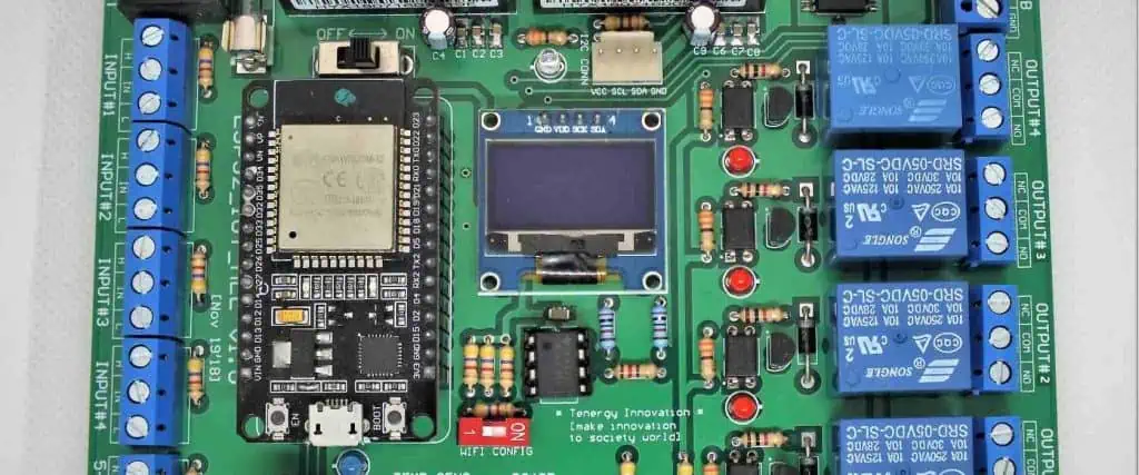
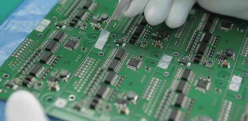
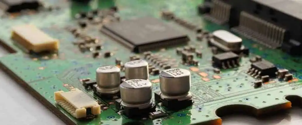
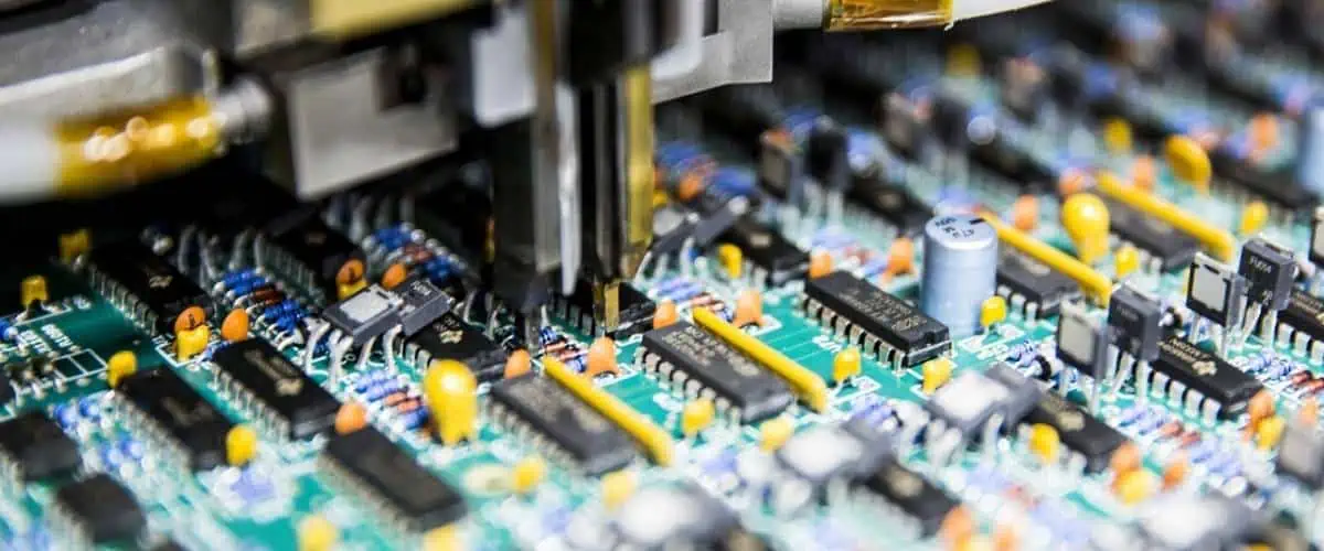
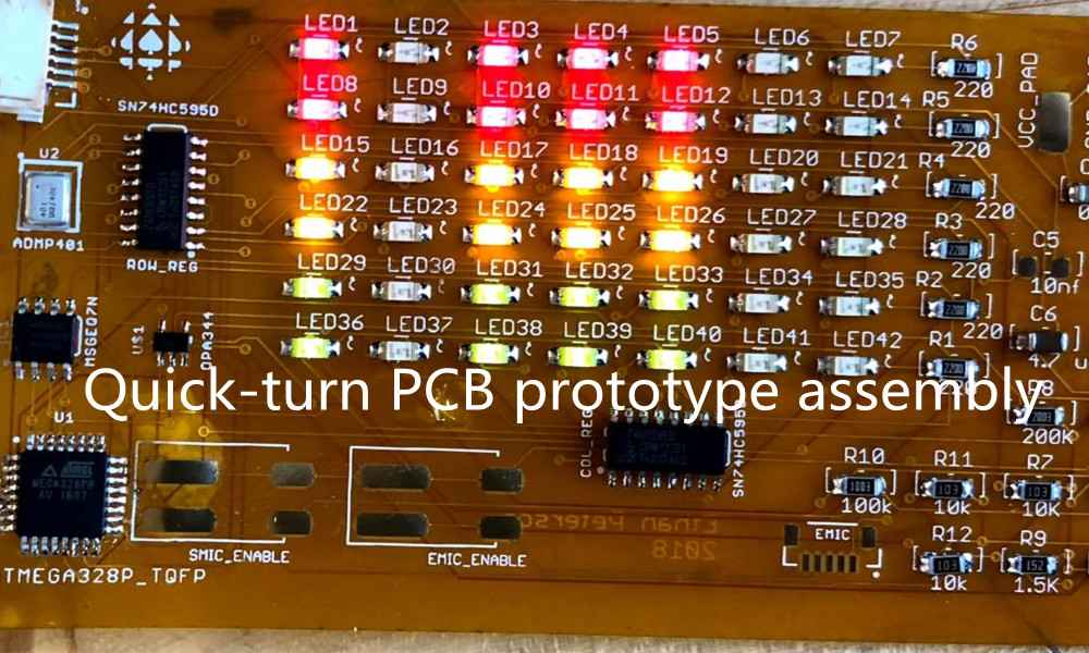
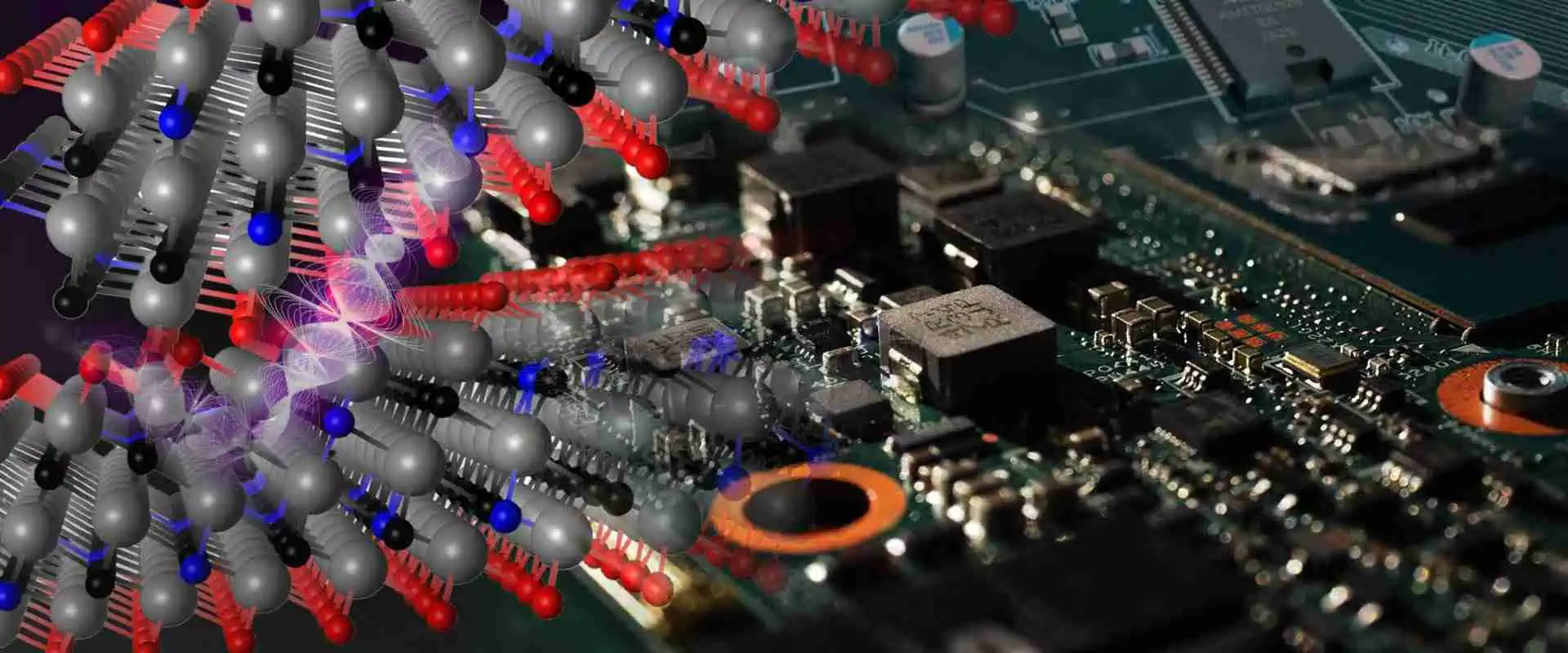
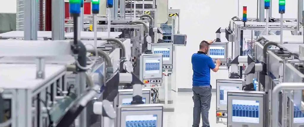
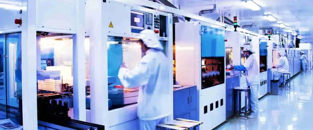
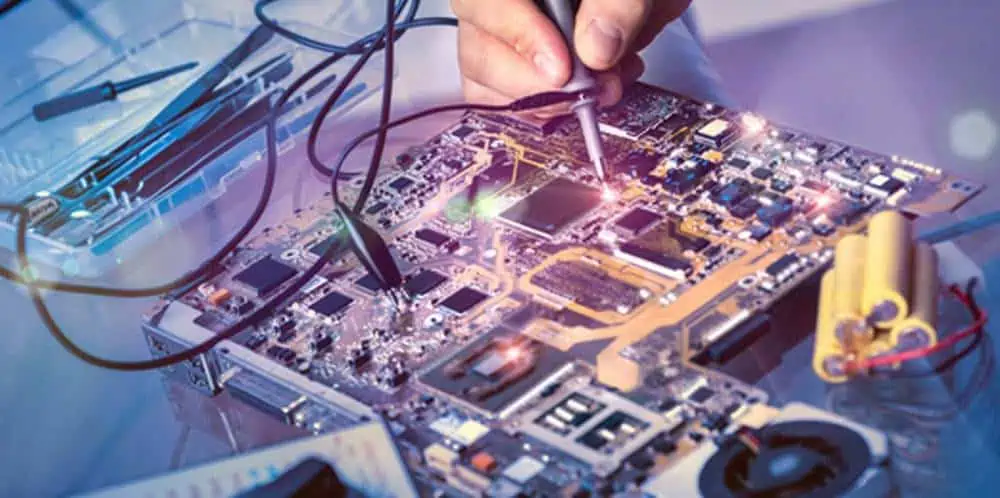
Electronics, out from the basic level of PCBs to a more ancillary sophisticated user interfaces, are essential in modern civilization. The increased demand for such items from consumers also increases the need for service providers in electronic manufacturing.

Yet, like an electronics organization that wants their electronic manufacturing services demand satisfied, it becomes crucial to choose a reputable manufacturer to assure high-quality production and finished products. Therefore, how should you do this in Netherlands?

How to Choose the Best Electronics Companies in Netherlands

Industrial electronics manufacturers

You must get in touch with the greatest electronic manufacturing firm in order to receive the best assistance for your electrical needs. This manufacturer will guarantee the electronic product’s quality while maintaining quality consistency regardless of volume. In addition, the manufacturing firm will provide you with outstanding support as well as designing, prototyping, plus production-related services.

So, you must make the right choice to avoid choosing an EMC which cannot meet your needs for electronics manufacturing. Along with the standard baseline factors like recommendations, EMC ratings, from experienced and reliable sources, personal tastes, and web evaluations from prior and present clients, you should consider the inquiries that follow to make sure you get things right.

Does the company providing the electrical manufacturing services have a long history and substantial industry experience?

Selecting a partner for electronic manufacturing might be difficult, but it always leads to assessing the reputation and history of electronics companies in Netherlands, particularly the one that you wish to go into.

Regarding the successful manufacturing of electrical items, the amount of time an EMS supplier has been in business becomes crucial. In addition, the manufacturer’s expansion within the same time period is crucial since it suggests that they can consistently satisfy the wants of their customers within the market sector.

Is there a way these electronics companies in Netherlands can improve the design process?

A number of EMS providers often provide some support during the DFM process. As a result, it is crucial to continually search for electronics companies in Netherlands with the most up-to-date toolkits, clear and concise design rules, readily available knowledgeable and qualified employees, and a proactive attitude. It will help your products reach the market more quickly.

Can you clearly identify the EMS provider’s investment in contemporary technology and cutting-edge equipment?

You could only rely on a reliable EMS provider that can meet your objectives for electronic manufacturing through implementing cutting-edge testing and production technologies in addition to exhibiting a strong commitment to ongoing investment.

Would the EMS provider follow all rules and norms for electronic manufacturing?

FULL PCB MANUFACTURING Quote

All major electronics companies in Netherlands fully comply in numerous industry criteria that appear in certificates. Demonstrating such a capacity suggests the dependability and accuracy of your EMS provider in Netherlands to ensure quality output, even though attaining and retaining such qualifications in extremely tasking manufacturing environments proves challenging.

How thorough is the Product Testing Program of the EMS Provider?

Product testing will become an essential step in the production of electronics. For electronic equipment intended for extreme environmental conditions, it’ll become especially important. If the EMS provider possesses access to these facilities, they can show to be the best choice for all your needs involving electronic manufacturing.

Would these Electronics Companies in Netherlands fulfill orders after they are placed?

Particularly, regarding the type of support provided after the production stage, assurances are always crucial. Component engineering management services, full support throughout the product lifecycle, including component lifespan management are a few examples.

Are these Electronics Companies in Netherlands communicating in a clear and efficient manner?

Any high-quality process of electronic manufacturing always becomes centered around information flow. As a result, these top electronics Companies in Netherlands must exhibit consistency, teamwork, and communication. These factors will enable engaged conversation, which will also ensure easier and faster decisions for business.

Does the EMS supplier have the flexibility to handle all product revisions and adjustments promptly, regardless of how they might affect the current production?

It particularly applies to companies built for high-mix low-volume operations since they need to show that their business processes and systems can adapt to sudden changes.

Exists a new product launch procedure at the prospective EMS partner?

Regarding design reviews, cost awareness, volume ramp, as well as product validation, top electronics Companies in Netherlands must have a pipeline approach in place in order to assure understanding and respond to all of your manufacturing and design demands.

Is there a good cultural fit with this Electronics Companies?

The best electronics Companies in Netherlands must speak a language that is equivalent to the OMC. It aids in understanding the requirements for design and production in order to deliver high-quality electrical products on schedule. So, before choosing an optimal EMS suitable for your production needs, you must take this element into account.

Does the production footprint of the EMS supplier match your immediate and future needs?

The ideal electronics Companies in Netherlands for you would be a Company, which can both fulfill your long-term strategic objectives and your current needs for electronic production.

What is the provider handling plan for traceability?

Electronics manufacturing relies heavily on traceability since it enables tracking of production, matching of replacement components, and product recalls in the event of technical or unforeseeable difficulties.

Does the production mix of the EMS Company satisfy the requirements for your products?

While choosing a manufacturer of manufacturing solutions, it becomes crucial to understand the portfolio setup and company infrastructure. It will assist in ensuring that you chose the appropriate EMS provider.

Is there a structure in place at these Electronics Companies in Netherlands to keep track of service levels?

These consumer-oriented activities comprise VOC programs as well as assure customer satisfaction whenever the production process concludes.

Best Electronics Companies in Netherlands

Microelectronics Manufacturing

Neways Electronics

This is one of the best electronics companies in Netherlands, formerly known as Elektrotechnisch Projecten Bureau Meulensteen, was founded in 1969. It offers specialized services for the entire lifecycle of a product of electronically controlled systems as well as electronic components. Also, I t offers high-quality EMS services to the automotive, defense, semiconductor, industrial, medical, as well as other industries. It is situated in the Science Park in Eindhoven Ne.

Business highlights include long-term collaborations, multi-certification, and lifecycle partnerships. The following services and products are provided: PCBA, Box Building, Hybrid microelectronics, System integration, Wires and Cables, Design and development, Manufacturing, Material management, as well as After-sales services.

Remeha

This is another top electronics company in Netherlands established in 1935 and specializes in solar energy, biomass boilers, hot water, heat pumps, as well as heating systems. The business is equipped with the most recent technology, talented workers, and contemporary machinery to produce high-quality electrical goods for many industries.

Its main office is in the Gelderland area of the Netherlands.

Highlights of the company include:

  • Producing sustainable as well as diverse solutions for heating
  • Certification and compliance with industry requirements surrounding product safety
  • About 500 employees worldwide;
  • A division of the BDR Thermea

The items offered include Thermostats, heat pumps having high power, hybrid heat pump, electric heat pump, heating boilers, and sunlight systems

Vanderlande

The business operates as a global provider of services for electronic manufacturing that deals with the automation of transportation processes. It was founded in 1949 and has since received certification, a staff of highly qualified specialists, cutting-edge technology, and cutting-edge equipment to assure high-quality services for the product lifecycle for your happiness. It is situated in the Dutch province of North Brabant.

Business highlights

  • Lifecycle services (logistics, business, as well as asset services).
  • Focuses on manufacturing and electronic innovation
  • multiple certifications, as well as industry compliance
  • Close client collaboration to enhance delivery

Products provided include

  • Systems (transportation, check-in, security checks, Bag Storage, Bag Sortation, Make-up, Transfer and Unload Break).
  • Softwares (VIBES, monitoring and reporting tools, PAX Multiplex software for screening, and PAX Checkpoint)

TKH Group

This highly regarded company in the field of electronic manufacturing was founded in 1930 and specializes in creating and producing high-end technology. Via development and research, engineering, marketing, process development, production, logistics, as well as project management, the company offers superior electronic solutions.

Its headquarters is in Haaksbergen area of the Netherlands.

Business highlights

  • Aims at the building, construction, as well as industrial sector
  • Decentralized management structure
  • High responsiveness to client needs and market prospects
  • Certification as an ethical and legal EMS provider

Items provided

  • Telecoms: copper cable system, fiber optics, parts, and systems, including SAODF, site management systems, including smart access technologies.
  • Building solutions
  • Industrial Solutions

Lumileds

From its founding, this Company has provided lighting solutions for more than a century. It focuses on the creation, production, and distribution of LED and automotive lights. It takes great satisfaction in its ability to develop high-quality lighting solutions and products through innovation and certification. It is situated in the Dutch province of North Holland.

Business highlights

  • Almost a century of experience in the field
  • Production of innovative lighting solutions
  • Accredited manufacturer
  • Display, UV, infrared, and flash are among their specialties

Items provided

  • LED bulbs and modules
  • Integrated LEDs
  • Single die LED
  • Infrared technology

Signify

The company providing electronic manufacturing services was founded more than 125 years back and is a market leader throughout the lighting industry. It concentrates on creating lighting products for the Internet of Things, industry, and consumers. This business is based in Eindhoven, North Brabant, in Netherlands.

Business highlights

  • Provides lighting products under several brand names
  • Has expertise in supply, manufacturing, and innovation;
  • complies with different industry standards;
  • emphasizes sustainability; and
  • offers customization services

The following services are provided: professional services, managed services, and lifecycle services (essential package, remote package, as well as premium packages)

NXP Semiconductors

This company has more than 60 years experience in advancing technology and offering electronic goods and services. It strives to safeguard infrastructure and connections for a developed and intelligent world in the present day as well as the future. The business is based in the Dutch city of Eindhoven.

Business highlights

  • Target several industries, including the automotive, communications smart home, infrastructure, and smart city
  • Dedicated to sustainability

The following products are available: Arm processors, all processors, Arm MCUs, and application-specific products etc.

Philips

Philips is an EMC with more than 130 years of experience that specializes in product manufacturing, primarily for the medical or healthcare industry. It offers top-notch electrical items since it has certified employees, cutting-edge technology, and equipment of the finest quality.

It is situated in the Dutch city of Amsterdam.

Business highlights

  • Produces and supplies medical equipment
  • embraces innovation
  • more than 130 years professional experience
  • produces high-quality goods
  • Complies with the industry regulation

Products Offered

Items available include consumer goods like electric razors, toothbrushes, lights, etc. and professional healthcare goods.

ASM

This company, which was founded in 1968, is recognized as a leader in the field for offering licensed and excellent manufacturing services. Excellent facilities, cutting-edge technology, and a knowledgeable personnels enable it in producing high-quality manufactured products.

It is situated in the Dutch city of Almere Stad.

Company highlights

  • More than 52 years of experience
  • many manufacturing facilities
  • features specific to semiconductor industry
  • adherence to the industry standards and regulations

Products available include: Plasma enhanced vapor deposition with chemicals, Plasma enhanced ALDs, deposition of atomic layers, Low-pressure diffusion of chemicals as well as vapor deposition, Epitaxy, and goods.

Conclusion

When you choose the best electronics Companies in Netherlands, they might become your perfect destination for all of your electronic manufacturing needs. I hope you now completely comprehend the steps required to choose a great EMS service.

Why is EMI Insulation necessary?

EMI Insulation

We live in an era full of EMI (electromagnetic interference)โ€”the many gadgets we utilize daily, such as phones and laptops, cause these EMI interferences. Moreover, various natural phenomena also cause EMI disturbance, for example, lightning. Generally, we, as humans, can’t feel EMI. However, multiple types of electronic and electrical gadgets can.

When electronic gadgets receive excessive amounts of EMI, they can become unreliable due to reduced performance. That is why modern electronic and electrical manufacturers install EMI insulations in their gadgets to eliminate or reduce electromagnetic interference. These impeccable electromagnetic shielding systems utilize multiple methods to shield your essential gadgets from EM interference.

Suppose you manufacture, use, or design electronic and electrical gadgets prone to EMI. In that case, you must have basic knowledge of EMI shields, how they work, and how to deal with them effectively. Moreover, you should be able to answer EMI-related questions with ease. For example, what are the effects of EMI? Why should you utilize an EMI shield on your gadgets? And what are the effects of not installing EMI shields on electrical and electronic devices?

YouTube video

EMI in a Nutshell

low-frequency EMI shielding

EMI basically refers to the transmission of harmful or unwanted EM radiations to an electronic or electrical gadget. These EM signals can disrupt the normal operations of a device, ultimately lowering its performance and reliability. Electromagnetic interference can emerge from various sources, both man-made and natural.

Common workplace and household gadgets are among the most popular EMI sources. Some devices like TV remote controls generate relatively weak and small EM fields. Other gadgets like smartphones and ovens generate stronger and more powerful EM fields. When these EM fields move from the source to the receiver, they have the potential to generate detrimental interference.

Moreover, EMI does not have to emerge from outside sources. It can also arise from internal sources. Internal electromagnetic interference refers to when the components of a device cause EMI to another element in the same gadget. Moreover, upstream issues with the conditioning and quality of various power sources also cause EMI to multiple gadgets. And when these kinds of internal electromagnetic interference come together, they can generate tough problems that can be challenging to fix.

Electrical gadgets aren’t the only culprits when it comes to causing EMI. Nature itself tends to generate electromagnetic interference. In addition, various atmospheric phenomena like solar storms and thunderstorms, tend to emit EM radiation naturally. Though natural, these radiations can also have detrimental effects on various electrical gadgets.

In the discussion about EMI, you might also hear the term RFI or radiofrequency interference. Most people tend to utilize these two terms interchangeably. Radiofrequency interference is an EMI subset that resides in the broad EM spectrum called the RF or radio frequency band. RF is also a pretty popular interference since multiple gadgets, including prevalent types of electric motors and power-switching gadgets, can emit RF, causing radiofrequency interference.

Major Types of Electromagnetic Interference

FULL PCB MANUFACTURING Quote

When it comes to EMI, you’ll find that there are two main types of electromagnetic interference that cause the most interference in electronic and electrical gadgets. Once you differentiate these two forms of EMI, you will be able to pinpoint and analyze the source of electromagnetic interference in your gadget and then devise an effective strategy to handle the situation.

These major types of electromagnetic interference are the following:

Ambient EMI

Ambient EMI, which also goes by the name radiated EMI refers to a type of electromagnetic interference that originates from natural phenomena or another gadget. Common workplace and household gadgets are the most popular causes of ambient EMI. However, some natural phenomena, for example, lighting and solar magnetic storms, also cause ambient EMI.

Power Quality EMI

Power quality electromagnetic interference, which also goes by the name conducted EMI, originates due to various inconsistencies and disturbances in a device’s power supply. These include line noise, voltage spikes and sags, and power interruptions.

Some EMI subsets affect systems and devices in various application types. The most crucial application-specific electromagnetic types are the following:

Intentionally Generated Electromagnetic Interference

Intentionally generated electromagnetic interference is a type of electromagnetic interference that comes from various phenomena, for example, NEMPs (nuclear electromagnetic impulses), that the military utilizes to disrupt the operation of various gadgets.

The intentionally generated electromagnetic interference is just a crucial factor in some operations, for example, critical infrastructure and military systems. However, you must utilize intensive precautions to combat this type of EMI.

Mass Transit and Railroad System EMI

The various electrical systems that technicians utilize to power modern-day rails transit are prone to various types of electromagnetic interference. For example, train control systems, third rails shoes, and other electrical and train supply lines can ultimately generate EMI, which can affect nearby gadgets, causing pretty adverse outcomes.

Medical Gadget EMI

Clinic and hospital environments have multiple devices that can receive and emit electromagnetic interference; this includes common devices such as:

  • Imaging machines
  • Drug pumps
  • Patient monitoring systems

These gadgets generate pretty high levels of ambient electromagnetic interference in most healthcare settings. Moreover, with the emergence and integration of Medical IoT gadgets in hospitals, you can expect this situation to worsen with time.

Significant Consequences of Electromagnetic Interference

PCB Design Guidelines For EMI EMC

RFI and EMI can affect various types of tech and can ultimately cause many problems. Here are the most common issues that emerge as a result of EMI:

  • General technological difficulties and malfunctions
  • Fires and overheating
  • Interference with monitoring and control systems
  • Difficulty in terms of establishing wireless connections
  • Audio and video signal distortion

Gadgets that are more vulnerable to EMI

Various electrical and electronic gadgets are vulnerable to electromagnetic interference. However, these are the gadgets that are more vulnerable to this interference:

  • FM and AM radio
  • Broadcast TVs
  • Walkie-talkies
  • Baby monitors
  • Smartphones
  • GPS systems
  • Computers
  • Wi-Fi routers
  • Medical devices

EMI Insulation: Common Techniques and Tools

EMI insulation (shielding) is basically the act of utilizing various countermeasures on electronic and electrical gadgets to shield them from EMI. The most popular methods of electromagnetic insulation include:

Electrical Enclosure Boxes

Suppose you seek the assistance of professional electrical gadget designers on the topic of EMI insulation. In that case, they will probably advise you to utilize an EEB (electrical enclosure box) on your device. Electrical enclosure boxes are basically boxes that are made using conductive metals, for example, steel and aluminum, which effectively shields the gadget from EMI. Moreover, constructing the electrical enclosure well will effectively redirect and absorb the EMI instead of letting it reach the components inside your device.

To generate electrical enclosure, technicians primarily utilize the following metals:

  • Silver
  • Copper
  • Aluminum
  • And different variations of steel

Technicians prefer these metals due to their resistance to electromagnetic interference, which comes naturally.

EMI Insulated Gaskets

For further mitigation of EMI, you can also equip your gadget’s electronic enclosure with EMI-insulated gaskets. These gaskets encompass standard components, for example, neoprene. However, they also encompass conductive linings, for example, wire mesh or expanded aluminum, that turn this gasket into an effective conductive barrier that you can use for EMI shielding.

Conductive Spray Coatings

Another technique that you can utilize for EMI shielding is applying a conductive coating via the utilization of a conductive spray coating. Generally, these conductive coatings encompass conductive metals, for example, nickel or copper, in a format of a spray-on. You can then utilize this spray-on on non-conductive components, for example, polycarbonate. Applications of a conductive spray coating provide an effective technique to add electromagnetic interference resistance on a wide variety of gadgets.

EMI Shielded Cables

You can also utilize EMI-shielded cables to effectively combat the multiple EMI issues that occur in electrical cables during the process of transferring current. For example, cables can receive and emit EMI. Therefore, the utilization of EMI-shielded cables tend to minimize the occurrence of both receiving and causing EMI.

If you want to combat EMI effectively in your device, you should significantly consider utilizing EMI-shielded cables in your project.

Electronic Filter Circuits

Most electrical and electronic gadget designers utilize electronic filter circuits on their devices to help in terms of better shielding the device against EMI. Moreover, electronic filter circuits come in multiple variations to fit different projects. Furthermore, you can recalibrate these filters to help them reject and accept specific frequencies. You can utilize this feature to make your shield more flexible and efficient in terms of controlling electromagnetic interference.

EMI Insulation Foil and Tape

EMI insulating foils, films, and tapes each bear their unique places in the electromagnetic insulation market.

Electromagnetic interference shielding materials tend to come in various shapes. For instance, conductive silicone functions impeccably as a window film that helps in terms of shielding electronic components from electrical and magnetic signals in commercial areas.

The component that you utilize to shield your gadget from EMI will depend heavily on two factors:

  • The frequency that you are dealing with
  • And the electronic component that you are shielding

For instance, you can utilize plaited braids and metallic foils to shield electronic cables from EMI. The foil can act as an impeccable component if you are looking for a substitute for EMI-shielded cables. To achieve this feat, you must wrap all the wires in your gadget with a conductive foil to make it resistant to EMI.

Moreover, you can also cover various connectors with this foil to give the gadget complete protection against EM interference.

However, when the magnetic fields hit 100 kHz and above, you will have to utilize magnetic materials and conductive points to deal with EM interference better. Technicians will also utilize mesh metal screening, conductive plastic, and metal foam.

Shielding tapes tend to be pretty ideal for EMI insulation due to a couple of reasons. For one, they are flame retards, and they are resistant to corrosion. Moreover, they are also embossed and flat, which makes them pretty ideal for effectively shaping around various odd shapes and corners.

Shielding tapes are primarily present in the following components:

  • Electronic medical devices
  • Keyboard components
  • Ground panels for connectors and electronic cables
  • Panels and doors of various electronic cabinets
  • Around outside relays and coils

Electromagnetic Mitigation Techniques

Electromagnetic mitigation methods are often adequate substitutes for EMI shields. These methods can include:

  • Erecting a wall between two gadgets
  • Placing devices facing different directions

In rare cases where the electromagnetic radiation levels aren’t high, you can utilize these techniques solely to combat EMI.

Crucial Aspects of EMI Insulation that you should keep in Mind

EMI shielding materials

Electromagnetic interference is a pretty complex phenomenon, and it can interact with various gadgets, circuit pathways, and materials in unpredictable ways. However, these are the most crucial aspect of EMI insulation that you should keep in mind:

Devices that rely on RF Signals to Function

Some gadgets, for example, key fobs and Wi-Fi routers, tend to rely on RF signals to transmit information wirelessly. However, metal enclosures that various other technicians utilize to block electromagnetic interference can also unintentionally block RF signals coming from these gadgets. If you find yourself stuck in this situation, you should utilize a polycarbonate enclosure which tends to function more efficiently in such applications.

Gaps and Seams

The performance of an enclosure can be affected negatively by gaps and seams that have not been secured properly. In addition, even tiny apertures in these enclosures can allow electromagnetic radiation to enter or leave the gadget, causing adverse effects. To effectively combat this issue, you can specify your enclosure with body designs that are continuous. Doing so will minimize the amount of EMI passing or entering your device.

The Ground Facts

The ground is an excellent source of persistent electromagnetic interference. That is because high impedance grounds with high frequencies can generate noise voltage that tends to be pretty challenging to eliminate. However, to combat this issue, you can utilize low-impedance grounding methods, which work perfectly.

Conclusion

Electronic and electrical components have become a significant part of the human race. You can find this component in multiple crucial industries, for example, the medical industry and the military sector. Moreover, we also utilize them to carry out various everyday tasks, for example, baking using an oven. Due to the crucial part that these components play in the human race, we expect them to be functional and reliable. Therefore, to ensure that this is the case, we have to combat common hazards that seek to compromise the functionality and reliability of electronic and electrical gadgets, for example, EMI. We hope this article has provided you with all the information you need to combat EMI effectively.

A Comprehensive Guide to the Top Pads Schematics

Pads Layout Viewer Download

PADS is a powerful software for PCB design that facilitates the creation of schematics, board layouts, and overall circuit design. With its comprehensive tools, PCB designers can achieve optimal board layouts efficiently. PADS is offered in three different versions to cater to different needs. This tutorial on PADS PCB design is perfect for novices as it guides them through the exploration of the software, from circuit board design to schematic entry.ย 

What are Pads Schematics?

PADS, a sophisticated printed circuit board design software developed by Mentor Graphics, boasts a robust and user-friendly interface. It is a popular choice among engineers & designers, and its capabilities ensure a successful design. PADS enables you to seamlessly navigate the entire electronic design process, from prototype to production, within a user-friendly environment. With just your desktop, you can connect with multiple industry professionals and collaborate with them to achieve your design goals. 

PADS offers three distinct versions, each tailored to the specific needs of different user groups. The versions are Standard Plus, Standard, and Professional, each with unique capabilities. PADS is a cutting-edge, commercial-grade software package with a broad range of advanced features, such as thermal design analysis, signal analysis functions, & advanced auto-router.

Engineers whose primary focus is printed circuit board design & schematic capture will find that the PADS Standard version is precisely tailored to their needs. This version boasts impressive capabilities, such as robust search & filtering tools, IPC-compliant patterns, & component selection. 

The PADS Standard Plus software is tailored to meet the needs of hardware engineers seeking efficient verification & analysis capabilities. It boasts a centralized parts library and advanced signal integrity features like crosstalk. On the other hand, the PADS Professional software is the ultimate choice for engineers who require a comprehensive software solution.

YouTube video

Features of Pads Schematics

PCB Layout in KiCA
PCB Layout in KiCA

The PADS printed circuit board design software incorporates cutting-edge features that simplify the PCB design process. Moreover, these advanced capabilities greatly enhance the software’s efficiency in accomplishing PCB design tasks.

ยท Analog simulation

The PADS printed circuit board is a sophisticated model subject to meticulous scrutiny. This layout software is also instrumental in simulating both mixed-signal & equivalent circuits.

ยท Component data organization

The PADS printed circuit board represents a highly advanced PCB model that undergoes rigorous examination. Additionally, this printed circuit board design software plays a pivotal role in emulating both mixed-signal & equivalent circuits. 

ยท Broad electrical rule check

Incorporating precise layout rule screening within PADS facilitates the validation and assessment of intricate design rules.

ยท Variant reprocessing and management

PADS printed circuit board design software enables users to incorporate a single schematic into multiple design layouts & workflows.

ยท Power-integrity examination

This functionality aids designers in identifying any potential power circulation issues before commencing the PCB layout process. Additionally, it can detect IP drops.

ยท Design Multi-Trace HSD

By incorporating program tasks and high-speed capabilities, this feature can minimize the time required for design.

ยท Thermal assessment

PADS offers a thermal evaluation feature that enables you to analyze design concerns and generate temperature maps for PCBs at the board level.

Use Pads Schematics PCB Design Software

FULL PCB MANUFACTURING Quote

ยท Schematic capture

A schematic is a visual representation of a circuit board’s design that includes connectivity and design rules. This crucial feature enables users to obtain data in multiple formats and gather the necessary information to input into design simulations and plots.

Moreover, the schematic is a dynamic design database containing component characteristics & tolerances. To create a schematic in PADS, navigate to the software’s start page and select the “Create” tab, where you can customize the features of your chosen components. Additionally, PADS PCB software offers a sample and features a toolbar that includes various displays and functionalities.

In addition, you can utilize any of the available features & displays to create personalized designs. Once you have created the schematic, it’s essential to verify the functionality of your printed circuit board design. You can accomplish this by navigating to the Libraries section and selecting “Common,” followed by the Central Library Synchronization, which enables you to check for any PCB parts that may be causing issues. 

ยท Component management

PADS provides component handling functionality, which grants users access to all component data. The management system eliminates the need to manage multiple libraries or data redundancy. PADS printed circuit board design also seamlessly integrates with MRP databanks, allowing designers to access critical components easily. Additionally, PADS updates the database, ensuring that all information is current.

PADS’ component manager fulfills multiple functions, including the ability to locate specific components by entering search criteria. When a search is conducted, the software displays all available components. To optimize your search, additional details, such as the tristate output, can be inputted. Furthermore, PADS provides the number of components that meet the specified criteria, further streamlining the search process. 

It is important to thoroughly examine the participant elements & their parameters when reviewing a component. One way to access detailed component information is through spreadsheet links, which allow you to view the component datasheets. It can offer you extensive and valuable data regarding the component.

ยท Include Generic Components in Pads Schematics

When selecting a PCB manufacturer, PADS software displays all available options once you have selected the necessary parts. The software also provides information on different parameters, such as inventory and inventory level.PADS layout capabilities can be leveraged to create advanced circuit boards, regardless of complexity. PADS can handle the whole design process, from production preparation to advanced 3D layouts and physical design reclamation, enabling users to design much more quickly. Additionally, PADS enables users to finish their circuit projects swiftly, providing the necessary information to make informed decisions. The PADS software has a feature called part management that can identify design parts that don’t have a unique brand name and can also help fix mistakes in the property information.

ยท PCB Layouts

You can expect a high-quality end product with Standard Plus Pads. This version of Pads also provides additional benefits such as fast signal routing and time-saving Design for Test (DFT) reviews. It’s important to note that all versions of Pads include Pads Outline, as well as a complete 3D visualization of the PCB that includes traces, solder masks, pads, and more. This photorealistic view helps to facilitate accurate assessments of the PCB before the fabrication of the end product. 

Moreover, 3D visualization enables users to obtain a clear and unobstructed view of the PCB’s internal stack-up, providing the necessary information for designing customized boards. Additionally, one can gauge the minimum distance between objects to determine their relative positioning accurately. Furthermore, PADS allows for including features such as heatsinks & covers.

With PADS design feature capabilities, designing high-performance printed circuit boards is made easy and efficient, regardless of the complexity of the circuit involved. PADS layout is a regular part of Altium’s Select Design feature for all PADS settings.

 Import a Circuit Design From Pads Schematics Layout into Altium

esp32 pcb design
esp32 pcb design

ยท Install the Importer

The initial step is to set up the PADS converter alongside any other necessary exporters & importers. Afterward, activate the exporter & importers functionality by enabling it. Additionally, if required, support for PADS can be added from the customize the Platform page.

ยท Import PADS Files

To access the layout file importer in PADS through Altium’s Import Wizard, select the PADS ASCII Design & Library Files option. Then, you will be directed to the Type of Files to Import page, where you can import both schematic design files & library output files.

ยท Net Name Options

In PADS, establishing net connectivity can be accomplished through the utilization of net names, which are assigned as a property of the wire. Wires without a net name are automatically given an automatically generated name. Furthermore, Altium Designer offers a unique method of identifying nets that do not have a manually assigned name.

When importing a PADS schematic using the Wizard, an option to “Do not localize” hidden net names” is presented. 

Typically, all layout work in PADS commences on the logic page, which serves as the logical working area. PADS schematic layout files can comprise multiple schematic pages. In Altium, the virtual workspace begins with a document, and each document has a corresponding file saved on the computer’s hard drive.

ยท Check for Net Shorts in Pads Schematics

The wire possesses a characteristic called a net name, and when using PADS, a net name designated by humans is shown at the midpoint of the wire. If you import a PADS schematic into Altium, the net name marker may be located at the intersection of two nets. Therefore, it’s important to review the schematic and confirm the location of each label. You can relocate the netlabel by clicking & dragging it to an appropriate position, ensuring the corner connects to the wire of a corresponding net.

Limitations of Object Translation

ยท PADS Layout

When using a PADS layout, it is necessary to split physical design reuse blocks into individual parts as the software does not support them.

ยท PADS logic

Individual pin-type connectors are not supported by PADS logic. As a solution, It is possible to transform them into block-style connectors, resulting in all pins being included in a single schematic component.

Design a PCB with Pads Schematics

solidworks-pcb-design

This section will cover finishing a PCB using a PADS design.

ยท Select components

First, select the components that you require for the project. Once you have a list of components, gather their datasheets and check the recommended footprints mentioned in the datasheet.

ยท Design a footprint

For every element used in the PCB, it is necessary to create a corresponding footprint, which is the physical representation of the component. In most cases, the required footprints will already be available in the design library and can be reused multiple times within the same PCB. However, you may need to create new footprints for any unique components. It is crucial to verify that the existing footprints in the design library align with the mechanical dimensions of the used components.

Reference designs are available from certain companies like Texas Instruments and Freescale. 

ยท Schematic view of PCB

In this process, different components will be added to the PCB and connected using wires. To achieve this, Orcad can assist in creating schematics.

ยท Netlist and import it to PADS.

After creating the schematic, the netlist must be in PADs. The next steps involve defining the ground & power planes. It is essential to thoroughly check the printed circuit board for any potential errors at this stage.

ยท Generate Gerber files

Once the PCB layout has been designed, it is necessary to create Gerber files. PCB manufacturers use these files to produce the board.

To create the Gerber file, navigate to the “File” menu and select “CAM.” Typically, the Gerber file includes the following components:

To begin, press the “Add” button and proceed to choose the document type. Next, select “routing” and choose the top layer for layer association. Give the document a name and click on “preview” to see a preview of the top routing layer. Review the preview carefully to verify that there are zero errors.

Firstly, navigate to the “layers” option and choose “Top.” Additionally, select “Board Outline.” Clicking on “preview” will display the board outline. It is important to note that the circuit board outline must be in a file and should not be in either the top or bottom layer routing.

Follow the same steps for the bottom layer and the inner layer. However, it’s important to note that the board outline should not be added to the inner layers.

Once completed, the next step is to generate the “solder mask gerber”. Click “Add” and select “Solder Mask” under the document kind. Next, select the appropriate layer association and give the document a name.

Next, click “preview” to preview the upper solder mask coating. Review the preview carefully to confirm that all necessary details are present. It’s worth noting that there are multiple ways to display reference descriptions in silkscreen.

It’s also essential to confirm that the silkscreen includes additional text, logos, and serial numbers. This verification should be for the top and bottom layers to complete the silkscreen generation process.

To proceed, you need to generate a drill drawing. First, click on “add,” then choose “drill drawing,” and select “layer association.” To view the drill blueprint preview, click on “preview selection.” The preview includes three components: fabrication blueprint notes, a drill blueprint & drill table.

Conclusion

PADS is a professional software suite that caters to the needs of PCB designers. It has advanced functionalities that make it stand out in the market. In this article, we not only guided novices on how to integrate PADS into their printed circuit board designs but also delved into its essential tools. 

The essential IEEE IoT framework and standards

IEEE IoT

The IEEE Internet of Things (IoT) is a framework for enabling connectivity and communication between systems and devices. As a result, it allows the development of intelligent network devices. They can gather and share data, monitor and control processes, and optimize operations across various industries and applications.

The interconnectedness of systems, objects, and devices that enables them to gather and exchange data is known as the Internet of Things (IoT). The IEEE is a professional association dedicated to improving technology for the benefit of humanity. IEEE is significantly influencing the IoT ecosystem by creating standards and recommendations that promote compatibility and interoperability across diverse platforms, devices, and systems.

The perception, network, middleware, and application layers are only a few of the layers that comprise the IEEE IoT ecosystem. The perception layer has several sensors, actuators, and cameras that gather information from the surroundings. The network layer has several gateways and communication protocols that allow data to move between systems and devices. Various software elements that enable data processing, storage, and analysis are in the middleware layer. Finally, numerous IoT applications are in the application layer, which uses the data produced by IoT devices to offer value-added services to end users.

IoT primarily entails using software and cloud computing technologies to analyze and respond to data in real-time collected from the physical world via sensors and other connected devices, as well as other software to collect data from the physical world. This enables the development of intelligent systems that can decide what to do and how to do it depending on the data they gather, increasing efficiency, production, and cost savings.

YouTube video

Interoperability, scalability, security, and privacy are just a few of the fundamental ideas upon which we build the IEEE IoT framework.

Privacy

intel iot
intel iot

Several IoT (Internet of Things) standards the IEEE (Institute of Electrical and Electronics Engineers) created address privacy and security issues.

IEEE 802.11ah specifies the physical and medium access control layer requirements for wireless IoT devices. It is one of the most significant standards. In addition, this standard incorporates privacy-preserving features like encryption and authentication to guarantee the security of data sent between IoT devices and their networks.

IEEE P2413, another significant standard, offers a foundation for creating IoT architectures. This standard underlines the importance of building IoT systems with privacy and security in mind from the beginning.

In addition, the IEEE P2933.1 standard focuses on security and privacy in IoT systems. With the help of this standard, IoT developers may create systems that respect user privacy, reduce the gathering of personal data, and provide consumers control over their data.

Generally speaking, IEEE standards are crucial in ensuring that IoT systems and devices are created with privacy and security in mind, protecting user data, and preventing unauthorized access to IoT networks.

Interoperability

The IEEE IoT (Internet of Things) standards place a premium on interoperability, which is the capacity of various systems and devices to operate efficiently and effectively together. Interoperability in the IoT refers to the ability of devices from various manufacturers and operating systems to communicate with one another and exchange data in a standardized and reliable manner.

The IEEE IoT standards provide a common framework for assuring interoperability among IoT systems and devices. These standards provide the communication interfaces, protocols, and data formats that IoT devices must follow and the controls for handling data privacy and security.

For several reasons, interoperability is crucial. It first makes it possible to build a uniform IoT ecosystem where devices can easily interact with one another to enhance user experience. It also fosters innovation and competition by enabling various manufacturers to design devices that can cooperate rather than being restricted to proprietary systems. Finally, interoperability allows IoT devices to exchange data and resources more effectively, which can assist in lowering costs and boosting efficiency.

Interoperability is crucial to the IEEE IoT standards since it creates a unified and effective IoT ecosystem that can benefit consumers and enterprises.

Scalability

Connecting gadgets to the internet allows them to exchange data and communicate with one another, and this process is known as the Internet of Things (IoT). The IEEE IoT effort seeks to increase knowledge of and use of IoT applications and technology, including creating standards for IoT systems and devices. Scalability, which in this case refers to the capability of IoT systems to handle growing volumes of data and devices as they increase in size and complexity, is a crucial component of IEEE IoT.

Because IoT systems sometimes contain large numbers of devices and generate enormous volumes of data, scalability is crucial. As the number of devices grows, so does the volume of data they produce in an IoT system. Real-time processing and analysis of this data are necessary to derive insightful conclusions and inform wise choices. The system must also be capable of handling the boosted traffic and processing requirements that come with scaling up.

The necessity for effective and dependable communication between devices is one of the main obstacles to scaling IoT systems. IoT devices often connect to the internet and one another via wireless communication protocols like Wi-Fi, Bluetooth, or Zigbee. Unfortunately, the volume of traffic on these wireless networks also grows as the number of devices in the system does, which may cause congestion and performance problems.

Security

FULL PCB MANUFACTURING Quote

Several security features in the IEEE IoT (Internet of Things) standard aim to defend IoT systems and devices from various dangers, including illegal access, data breaches, and cyberattacks. Several of the IEEE IoT standard’s essential security elements are listed below:

Access control and authentication Only authorized users and devices can access the IoT network thanks to procedures for device authentication and access control included in the IEEE IoT standard. This lessens the likelihood of data breaches and illegal access.

Data protection and encryption: The IEEE IoT standard contains data protection and encryption features to help ensure that sensitive data exchanged between IoT devices and systems is secure and shielded from eavesdropping or tampering.

Security protocols: The IEEE IoT standard contains several security protocols, including the Transport Layer Security (TLS) protocol. It enables secure internet communication, and the Datagram Transport Layer Security (DTLS) protocol, which enables secure IoT device communication.

Updates to the firmware are allowed by the IEEE IoT standard. It helps keep IoT devices secure by addressing security flaws and issues that hackers could abuse.

Privacy protection: The IEEE IoT standard includes privacy protection clauses that help to guarantee that user data is gathered and processed in line with privacy laws and industry best practices.

The IEEE IoT standard offers a thorough framework for securing IoT systems and devices. Its security features address the particular problems IoT networks present. They include the high density of connected devices, the variety of communication protocols, and the limited computing power.

IoT-based ISO/IEC & IEEE Standards

ISO/IEC 30141

According to the organization, the Internet of Things (IoT) – Reference Architecture offers an IoT Reference Architecture that follows international standards. They assist in making linked systems safer, seamless, and more resilient. It intends to accomplish this by giving IoT application developers and designers a standard architecture. Additionally, it makes it easier to construct dependable systems which are dependable, privacy-friendly, safe, and resilient to interruptions like attacks and natural disasters.

It highlights non-functional requirements such as system maintainability, high availability, dependability, usability, scalability, and functional requirements. Therefore, by employing reference architecture, you can increase interoperability and make it easy for others to access your data while making enabling outsiders comprehend your system. You will realize that there are six domains with related entities communicating and exchanging data via a network.

The IoT reference architecture’s conceptual building blocks, which comprise the following:

  • Things are tangible things or gadgets connecting to available internet.
  • Devices that link things to the internet and perform protocol translation and other tasks include gateways.
  • Network infrastructure refers to the underlying network that links devices and gateways.
  • Services are platforms and software programs that give the Internet of Things ecosystem functionality.
  • Applications and analytics are software programs and services that use and analyze data produced by the Internet of Things environment.

The standard also offers instructions on creating and implementing IoT solutions using the reference architecture. It is intended for use by businesses engaged in the design, deployment, and administration of IoT systems and solutions and by academics and researchers working in the sector.

ISO/IEC 30165

The International Electrotechnical Commission (IEC) and the International Organization for Standardization (ISO) produced the ISO/IEC 30165 standard. It offers a foundation for real-time Internet of Things (IoT) systems.

Real-time IoT systems identify by their capacity to process and react to data in close to real-time, and the standard outlines their architecture, functionality, and interfaces. Furthermore, outlining standard interfaces and protocols seeks to guarantee interoperability and compatibility amongst various IoT systems.

The real-time IoT system requirements provided by ISO/IEC 30165 cover system architecture, data management, security, connectivity, and performance. It includes many uses, such as transportation, smart cities, healthcare, and industrial automation.

The standard can assist businesses in creating and implementing dependable, secure, and scalable real-time IoT systems. Additionally, manufacturers and service providers can use it as a guide to ensure their goods and offerings satisfy the needs of real-time IoT systems.

The IoT standards ISO/IEC 30165, IoT architecture, IoT reference model, IoT interoperability, and IoT privacy and security are all included in this series.

IEEE P1912

The design and implementation of ethical considerations for autonomous and intelligent systems are covered by IEEE P1912.

Moreover, IoT also presents ethical issues regarding privacy, security, and the possibility of data exploitation. IoT system designers and developers can follow P1912’s guidelines to ensure their creations adhere to moral standards and ethical values.

P1912 discusses the importance of creating IoT systems with transparency, privacy, security, and accountability. These systems should have security in mind and have the necessary safeguards to thwart malicious attacks or unauthorized access. They should also have processes for identifying and fixing any flaws or issues that may occur.

So, IEEE P1912 offers helpful advice for the ethical design and implementation of autonomous and intelligent systems. They include those that are a part of the Internet of Things. This is true even though it is not unique to IoT.

IEEE 1451-99

embedded iot

As a standard for smart transducers, the Institute of Electrical and Electronics Engineers developed IEEE 1451-99. (IEEE). An intelligent transducer is a device that combines a sensor or actuator with additional components. A microprocessor and communication interfaces communicate with other devices in a networked environment.

The IEEE 1451-99 standard defines several data formats and communication protocols that allow smart transducers to interact with other devices in a network. Since they are platform-independent, these formats and protocols can function with various smart transducers and network configurations.

The standard also contains a list of recommendations for building smart transducers that adhere to IEEE 1451-99. These suggestions cover the physical design of the transducer, its communication interfaces, and the data types it can support.

Overall, the IEEE 1451-99 standard provides a framework for developing intelligent transducers that may be integrated into many networked settings. As a result, it simplifies the collection and processing of data from various sensors and actuators.

IEEE P2413

The Institute of Electrical and Electronics Engineers (IEEE) established the IEEE P2413 standard. This standard outlines an Internet of Things (IoT) architectural framework. (IoT). The framework gives everyone a shared knowledge of the Internet of Things (IoT) and its numerous parts. They include devices, gateways, networks, and cloud services, as well as how they work together.

The standard aims to give IoT system developers a single language and infrastructure to aid interoperability, scalability, and security. Additionally, it offers instructions for designing and putting into practice IoT systems, along with suggestions for the application of open standards and best practices.

The IEEE P2413 standard includes three main components:

  • Architectural Reference Model (ARM): The ARM outlines the high-level organization of an IoT system, outlining all of its constituent parts and how they relate to one another. The ARM outlines an IoT system’s characteristics and features, including sensing, actuation, and data processing.
  • Architectural Ontology (AO): The AO offers a collection of ideas and expressions to apply to the elements and connections specified in the ARM. The AO attempts to give IoT stakeholdersโ€”developers, manufacturers, and usersโ€”a single language.
  • Reference Architecture (RA): The RA implements the ARM and AO and guides the creation of IoT systems. The RA also offers instructions on implementing open standards and best practices to guarantee security and interoperability.

By giving IoT stakeholders a uniform structure and vocabulary, the IEEE P2413 standard seeks to encourage the development of safe and interoperable IoT systems.

IEEE 802.15.4-2015

Smart Manufacturing IoT

A standard for low-rate wireless networks is IEEE 802.15.4-2015. The physical (PHY) and medium access control (MAC) layers are ideal for low-power & low-data-rate wireless networking. The standard accommodates various applications, such as intelligent energy, healthcare, industrial, and home automation.

The operating frequency ranges, modulation techniques, data rates, and network topologies employed by devices. These devices comply with the standard that are ideal within the standard. Additionally, it specifies the protocol and frame structure for data transmission between devices.

Star and peer-to-peer network topologies are supported by IEEE 802.15.4-2015. One device serves as the coordinator in a star topology, and all other devices communicate with it. In a peer-to-peer topology, all devices are capable of communication.

The IEEE 802.15.4-2015 standard’s low power consumption is one of its essential characteristics. As a result, devices that follow the standard can run on modest batteries or even energy-harvesting resources. Examples include solar panels for long periods. The standard is, therefore, perfect for devices that need a lot of battery life or are challenging to power.

Overall, the IEEE 802.15.4-2015 standard for low-power wireless networking is significant. It offers devices a versatile and effective method of interfacing with one another in various applications.

Top 10 IoT Companies and how to select them

IoT Device PCB BOARD

Complete automation is now feasible thanks to IoT. IoT is the only technology that makes solutions like smart cities, smart homes, smart factories, and connected vehicles conceivable.

This technology will, in fact, aid in simplifying corporate procedures, significantly increasing productivity in the process. In addition, you’ll be able to provide superior goods and services.

A firm that develops and offers Internet of Things (IoT) goods and services is known as an IoT company. The Internet of Things (IoT) is a network of physical items, including cars, homes, and other machinery. It can gather and share data online because they have sensors, software, and network connectivity.

Startups and huge corporations alike may create IoT businesses specializing in various industries, including smart homes, healthcare, transportation, and agriculture, among others. These enterprises may provide Internet of Things (IoT) tools, platforms, and software to assist organizations and people in streamlining operations, increasing productivity, and improving customer satisfaction.

YouTube video

Factors to consider when choosing IoT companies

ESP IoT Board
ESP IoT Board

The number of linked devices will reach 30 billion by 2025, representing a rapid Internet of Things (IoT) expansion. As a result, businesses now have more chances than ever to develop cutting-edge goods and services, boost operational effectiveness, and improve consumer experiences. As a result, the market is full of IoT firms that provide a range of corporate solutions. Choosing the best IoT business, though, might be difficult.

Expertise and Experience

The level of knowledge and experience an IoT firm has in the industry is one of the most important things to consider. Finding a business with a demonstrated track record of delivering successful IoT projects is vital. Look for organizations with expertise working with businesses comparable to yours and well-versed in the sector you operate in. You may find the best solution to match your business goals and steer clear of any hazards with the assistance of a firm with experience in IoT technology.

Scalability

Consider the scalability of a company’s solution when selecting an IoT provider. You should pick a system that can alter with the IoT market’s quick evolution and expand with your company. As your organization expands, a scalable IoT solution will let you add additional hardware, users, and features. Therefore, it is crucial to pick an IoT provider that can offer a scalable solution to fulfill your current and future demands.

Security

IoT devices send and gather sensitive data. Thus security is essential when choosing an IoT firm. A good IoT organization should have security safeguards to prevent unwanted access, theft, or exploitation of your data. They have to be able to provide you with a thorough security strategy that takes into account all possible dangers and threats. Seek out businesses with expertise in putting security measures like data encryption, two-factor authentication, and recurring security audits into place.

Integration Capabilities

IoT is not an independent technology. It must interface with other systems and programs to offer insightful data and add value to your company. Therefore, selecting an IoT provider with integration capabilities with other systems, including ERPs, CRMs, and BI tools, is crucial. Thanks to integration capabilities, you will be able to get data from many sources, evaluate it, and come to wise judgments.

Customization

Every organization has different demands. Thus you need an IoT solution that can be adjusted to fit your particular requirements. An effective IoT provider should be able to offer a personalized solution that supports the aims and ambitions of your organization. In addition, you should be able to add or remove features as needed, and the solution should be adaptable enough to develop as your business demands do.

Cost

When selecting an IoT provider, you should remember that IoT solutions might be pricey. Look for businesses with adjustable price structures that fit your demands as a customer and your budget. Also, consider the whole cost of ownership, which includes setup, upkeep, and upgrades. Finally, the IoT provider must offer a cost-effective solution that adds value to your chosen organization.

Support and Maintenance

IoT devices are complicated, so you need a business offering support and maintenance services to ensure your solution runs without a hitch. Seek out businesses that provide dependable support and upkeep services, such as remote monitoring, troubleshooting, and software upgrades. In addition, a strong IoT provider should be able to offer a proactive maintenance schedule that reduces downtime and guarantees your solution’s peak functionality.

Here are 10 of the top IoT companies

FULL PCB MANUFACTURING Quote

Amazon Web Services (AWS)

The Internet of Things (IoT) platform from Amazon Web Services (AWS) is a cloud-based system. It enables secure device connections and communication with AWS services. AWS IoT offers several services, including Device Gateway, Device Registry, Device Shadow, Rule Engine, AWS IoT Analytics, AWS Lambda, S3, and DynamoDB, that enable managing connected devices and the data they produce. These services include real-time and batch processing, machine learning, data visualization for IoT data, and sophisticated analytics capabilities. AWS IoT also connects with other AWS services, enabling the construction of sophisticated IoT applications.

Cisco Systems

Various Cisco Systems IoT (Internet of Things) services enable businesses to safely connect to, control, and analyze their IoT devices and data. These services include IoT Edge Computing, IoT Security, IoT Connectivity Management, IoT Data Management, and IoT Application Development. In addition, for IoT networks and devices, Cisco offers end-to-end security solutions, including secure device onboarding, authentication, authorization, and encryption.

With the help of IoT Edge Computing, businesses can process and analyze data from IoT devices at the network’s edge, requiring less latency and bandwidth while allowing real-time insights and actions. IoT Application Development offers enterprises the tools and platforms they need to swiftly and efficiently create and deploy IoT apps and integrate them with other corporate systems. In addition, organizations can securely connect and manage their IoT devices with the aid of Cisco’s IoT services, which provide them with the necessary tools and capabilities. This helps them increase productivity, efficiency, and customer experience.

Microsoft

A collection of cloud-based tools and services called Microsoft IoT, commonly called Microsoft’s Internet of Things (IoT) platform, assists companies and developers in creating, deploying, and managing IoT solutions. Using the platform, users may connect, monitor, and manage IoT sensors and devices across a range of sectors. They include manufacturing, healthcare, retail, and transportation.

Azure IoT Hub, Azure IoT Central, and Azure Digital Twins are just a few of the tools and services the platform offers to help customers connect and manage their IoT devices and data in a dependable, scalable, and secure way. In addition, to aid customers in deriving insights from their data and influencing better business decisions. It also contains a variety of analytics and machine learning capabilities.

The Microsoft IoT platform makes it simple for companies and developers to create and deploy IoT solutions using their chosen hardware and software since it supports many devices, protocols, and operating systems. Additionally, it interfaces with other Microsoft services like Dynamics 365 and Power BI to offer comprehensive solutions for various corporate requirements.

General Electric

General Electric (GE) provides a variety of IoT (Internet of Things) services to assist businesses in streamlining their processes and increasing productivity.

The Predix cloud platform from GE is excellent for developing and managing industrial IoT applications. Its system for gathering and analyzing data from numerous devices and sensors is safe and scalable. Asset Performance Management (APM) is an Internet of Things (IoT) system that employs sensors and analytics to identify possible problems. Additionally, they recommend preventative maintenance to avoid expensive downtime. Manufacturing companies may speed up their production lines and eliminate bottlenecks with Brilliant Manufacturing’s real-time data and analytics.

GE’s IoT services aim to reduce downtime and help businesses make the most of their operations. It uses real-time data and analytics to forecast and avoid outages, boost uptime, and ensure the smoothest possible power supply. In addition, companies may create a virtual representation of their physical assets using their Digital Twin technology, track their performance, and ensure that it is operating at its best. Overall, GE’s IoT services can assist organizations in making the most of their assets and increasing their productivity.

Qualcomm

intel iot
intel iot

Internet of Things (IoT) services and products are available from Qualcomm. Their Snapdragon processors are ideal for various IoT gadgets, including wearable electronics, smart home appliances, and business-related IoT equipment. They’re suitable for Internet of Things (IoT) devices since they are extremely powerful and consume little energy. In addition, they provide various wireless options, like Wi-Fi, Bluetooth, and cellular. They guarantee that your IoT devices are constantly connected, even in challenging environments.

Qualcomm’s Snapdragon Developer Tools provide a complete collection of tools and resources for developers building IoT devices. These resources enable developers to easily create and test their IoT applications. They do this by providing a variety of SDKs, example code, and documentation. In addition, to have more accurate and natural interactions with your IoT devices, Snapdragon Voice and Audio provides a powerful voice and audio processing for IoT devices, including noise reduction, echo cancellation, and speech recognition.

To help cities become more effective and safe, consume less energy, and have less impact on the environment, Qualcomm provides services and solutions for street lighting, smart parking, and intelligent traffic management. In addition,  Qualcomm’s IoT services and solutions enable you to create dependable IoT hardware and software for a wide range of markets and applications.

Honeywell

A variety of IoT (Internet of Things) services is available from Honeywell to assist organizations in streamlining their processes and increasing productivity. These services include asset performance management, supply chain, logistics, cybersecurity, linked buildings, connected employees, regenerate response, and asset performance management. Connected buildings leverage IoT technology to improve building operations and provide a more cozy, effective, and energy-efficient environment. Connected employees use IoT devices and analytics to help keep them safe and productive. IoT data and analytics are used in asset performance management to track and improve the operation of crucial assets.

Businesses may defend their IoT equipment and data with the aid of cybersecurity. Overall, Honeywell’s IoT services assist companies in leveraging IoT technology to boost operational effectiveness, increase worker productivity and safety, and gain a competitive edge.

Oracle

With the help of Oracle’s IoT services, you can connect, manage, and analyze data from your internet-connected equipment, sensors, and devices. Everything you require to manage your Internet of Things (IoT) devices and data is provided. They include a device connection that supports various IoT protocols, including MQTT, CoAP, and HTTP. Additionally, you receive a scalable and secure platform for gathering and storing your IoT data. As a result, it enables real-time processing and analysis for deeper insights and wiser choices.

Oracle IoT services offer cutting-edge analytics and visualization solutions to help you make the most of your IoT data. You may utilize your IoT data to optimize your business operations and satisfy your customers. This is because they are simple to link to your enterprise systems, such as ERP, CRM, and SCM. Naturally, they also offer total security, including device authentication, data encryption, and access control. As a result, it ensures the safety of your data. In conclusion, Oracle IoT services are the ideal method to maximize your IoT expenditures.

Ericsson

Ericsson IoT provides a variety of specialized goods and services, including IoT connection, IoT device management, IoT data management, and IoT professional services. The company also offers a variety of platforms and tools to support the development and deployment of IoT services and applications by enterprises and developers.

IoT solutions from Ericsson aid companies in streamlining operations and generating new income. Additionally, the solutions support many IoT use cases, such as smart cities, linked automobiles, industrial automation, and healthcare.

Ericsson IoT generally strives to offer complete, end-to-end IoT solutions. These solutions empower companies and organizations to harness the potential of connected devices and data to spur innovation and growth.

Huawei

esp iot
esp iot

The IoT platform from Huawei enables you to link various devices to the internet so they may communicate with one another and have centralized systems. It includes many tools and services to manage devices, analyze data, and make apps. Additionally, it offers a device management system that enables you to add, set up, and monitor your IoT devices. It may also operate the device and update its firmware remotely.

Huawei IoT offers a range of IoT device connectivity options. They include wired and wireless connections and secure data transmission utilizing TLS/SSL encryption. Additionally, it provides real-time data analysis and visualization features in addition to gathering data from IoT devices and storing it in a centralized database. Java, C, Python, and APIs are among the application development tools available for gaining access to the platform’s features. As a result, Huawei IoT offers a complete platform for creating and administering IoT applications. Additionally, it facilitates seamless interaction between devices and centralized systems.

Bosch

A global engineering and technology business headquartered in Germany, Bosch invented the Internet of Things (IoT) platform known as Bosch IoT. For developing and deploying IoT applications across several sectors and use cases, the Bosch IoT Suite offers a collection of cloud-based services and tools.

The Bosch IoT Suite comprises several parts, including connection, analytics, edge computing, device management, and data management. In addition, the platform supports a wide variety of IoT devices and protocols, including sensors, gateways, and edge devices.

Bosch IoT makes it easier and safer for companies and organizations to grow and execute IoT solutions. The platform can support sophisticated analytics and insights. As a result, it aids businesses in streamlining processes, enhancing their goods and services, and developing new revenue streams.

The Digital Hardware Design Process And Its Advantages

digital hardware design

Digital circuit design involves developing circuits capable of performing various tasks, from simple logical operations to complex computational functions. The process involves several steps, such as assessing the circuit’s requirements, designing, testing, and validating the design. This article provides a brief of the basic principles involved in digital circuit design.

Overview of Digital hardware design

Digital circuits utilize electronic signals that convey information in a binary format. These signals can only take on two values, 0 & 1, represented using voltage levels. Typically, a low voltage level, such as 0 volts, represents 0, while a high electric potential, such as 5 volts, means 1. Digital circuits can perform basic logical operations like OR and AND and complex computing projects such as arithmetic & logic operations.

Digital circuits can be classified into two broad categories: combinational and sequential. Combinational circuits produce an output based solely on the input values and do not have memory components. In contrast, sequential circuits use memory components & generate results based on past and current input values.

YouTube video

The Digital hardware design Process

hardware design engineer

Although the circuit design process includes various stages, the essential steps in this process are as follows:

ยท Requirement Analysis:

The initial step in designing a digital circuit is to identify its requirements. It involves defining the circuit’s purpose, as well as any design constraints such as power consumption, budget & performance standards.

ยท Design Specification:

The subsequent step involves creating a detailed design specification for the circuit, which includes a thorough description of its specifications. The design specification must specify the outputs, inputs, and behavior of the board for all possible input combinations.

ยท High-Level Design:

Once the design needs are established, the next step is to create an excellent circuit design. It involves selecting the components needed to make the circuit & establishing the connections between them to form the complete board. In addition to the excellent circuit design, a circuit diagram (block diagram) should be created to demonstrate how the different components are interconnected.

ยท Detailed Design:

During the detailed design phase, a circuit diagram known as the accurate circuit schematic is created. This diagram depicts the components & their interconnections. Additionally, selecting the specific transistors, resistors, and capacitors used to build the digital circuit is an essential aspect of this phase.

ยท Simulation and Testing:

After completing the circuit schematic, it is vital to conduct simulations and tests to verify that the circuit operates as intended. It involves subjecting the board to multiple scenarios, including different ambient variables & input values, by leveraging software tools to simulate its behavior.

ยท Fabrication and Testing:

Upon concluding the simulation & testing phase, it is necessary to construct and evaluate the physical circuit to verify its expected performance. Assembling the board with the selected components and evaluating its behavior under various circumstances to confirm its adherence to the design specifications is a crucial step.

Main components of a Digital hardware design

FULL PCB MANUFACTURING Quote

The fundamental components of the digital system merge to construct a system that can perform diverse projects. The unit executes operations on data residing in memory & processes instructions obtained from input devices. The system can also connect with other systems & devices using communication interfaces & showcase the outcomes. The primary constituents of the digital system are as follows:

1. Communication Interfaces:

Communication interfaces enable a digital system to connect with other components/systems. These interfaces can include USB ports, Ethernet connections, & wireless technologies such as Bluetooth & Wi-Fi. Through these interfaces, the digital systems can interact with other devices and systems, exchanging information & commands as needed.

2. Output Devices:

A digital system produces results from its computations showcased on output devices. Output devices can include printers, speakers, or monitors, among others. These devices convert the digital signals a digital system generates into a comprehensible format-comprehend.

3. Memory:

Memory is where data & instructions are stored for the processor to access. In the digital system, there are two primary forms of memory: primary & secondary memory. The processing unit temporarily stores data & instructions in primary memory, also known as RAM, while working on them.

4. Processing Units:

The processing unit is responsible for computing in a digital system. It usually comprises a microprocessor or CPU, which performs operations on the/digital data.

5. Input Devices:

Input devices provide input to a digital system. Examples of input devices include mice, touch screens & keyboards. These devices allow individuals to interact with input data and digital techniques through digital signals.

Advantages of Digital hardware design

PCB-mounting-hardware

Digital circuits utilize binary code that indicates the presence or absence of a current. These circuits are crucial in many electronic devices, such as computers, smartphones & televisions, due to their numerous advantages. Here are seven benefits of these circuits:

ยท Reduced Signal Degradation:

Digital circuits can transmit signals over very long distances with minimal signal degradation. It preserves the reliability of digital signals, allowing them to travel extended distances without significant loss of quality.

ยท Compatibility:

Digital circuits are widely compatible with modern electronic devices that utilize digital signals. It simplifies the process of integrating these circuits with electronic systems & devices.

ยท Flexibility:

These circuits are highly adaptable due to their ease of reconfiguration and reprogramming. It is possible to use discrete components, such as quickly replaceable gates, in digital circuitry.

ยท Low Power Consumption:

Binary signals, which have only two states, are advantageous in digital circuitry as they consume less power than an analog circuit. It is because changing the state of the signal requires less power.

ยท High Accuracy:

Binary signals clearly distinguish between off and on states, allowing digital circuits to function accurately. It enables circuits to perform precise actions without error.

ยท Easy to Store and Transmit:

These signals are easy to store & transmit because they can be represented utilizing binary digits. It simplifies the storage & transportation of extensive data, which is crucial for various applications such as digital storage, data processing & communication.

ยท High Noise Immunity:

Digital circuitry uses binary signals of low or high voltage to operate. Compared to analog signals, these signals are less susceptible to noise & interference. It makes the work of circuits more reliable and accurate.

Disadvantages of digital circuit

Digital circuits offer numerous advantages over other analog circuits, but they also have several disadvantages. Here are five disadvantages of these digital circuits:

ยท Propagation Delay:

Propagation delay refers to the time it takes for a signal to travel from one place to another within a circuit. For applications that require high speed, this delay can introduce latency errors into the digital circuit.

ยท Limited Frequency Response:

These circuits are limited in frequency responses compared to analog circuits. It is because the discrete elements used in these circuits are typically designed to operate at specific frequencies. So, the uneven frequency response of digital circuits may limit their efficiency in high-bandwidth uses, such as wireless transmission.

ยท Nonlinear Behavior:

While digital circuits can exhibit nonlinear behavior, they operate on binary signals that are either off or on. It’s because transistors can sometimes behave nonlinearly. This nonlinearity can result in unwanted harmonics, oscillations, or distortion.

ยท Limited Resolution:

While digital circuits operate at the specific voltage/current levels, measuring or regulating particular parameters may be tricky due to their low resolution. It can pose a significant problem for some applications, such as scientific instruments.

ยท Complexity:

Designing and constructing digital circuits may be more complex than analog circuits due to the discrete nature of digital circuits, which combine logic gates to make more complex circuits. As the number of gates in digital circuits increases, the complexity increases, making it troubleshoot.

Future of Digital hardware design

Online PCB assembly quote

The field of this circuit design is rapidly evolving and holds immense potential for creating innovative electronic devices and systems. These are the significant areas that will impact digital circuit design coming days:

ยท More Emphasis on Energy Efficiency:

As energy usage becomes a pressing concern, digital circuit designers emphasize energy efficiency more. Voltage scaling, DVFS, and power gating are some methods used to reduce digital circuit power consumptionโ€”furthermore, novel design approaches, such as approximation computing trade accuracy for power/energy efficiency.

ยท More Focus on Security:

With the growing danger of cyberattacks, the importance of designing safe circuits is increasing. Manufacturers use methods such as secure boot & HSMs to prevent unauthorized access & modification. Additionally, new encryption and authentication approaches are being developed to enhance the safety of digital circuits.

ยท More Advanced Design Tools:

With the increasing complexity of circuit designs, designers are adopting more sophisticated design equipment to handle the complexity and enhance circuit performance. HLS and AI are being used to automate the digital design process & improve the quality of the final design. Additionally, new simulation equipment simulates digital circuits efficiently and accurately.

ยท Higher Levels of Integration:

Digital circuit designers strive to make electronic devices smaller and more cost-effective. The integration of multiple functionalities, including memory, processors, and communication, into one package is being achieved through the adoption of SoC & SiP architectures.

ยท More Advanced Process Technologies:

To meet the demand for more powerful & energy-efficient devices, circuit designers are relying on increasingly sophisticated methods. Furthermore, novel materials such as graphene & carbon nanotubes are being explored for use in circuits due to their unique electrical properties.

ยท Assembly of Digital PCB

The assembly process for PCBs involves the utilization of software to oversee and manage the circuit board assembly. A digital thread connects the various stages of data reception & transfer throughout the assembly procedure, enabling real-time adjustments to improve or maintain quality.

It is essential to know that digital signals are a type of electronic signal generated rather than occurring naturally. Generating these signals can result in countless signals, particularly when considering the controlled aspect. Thus, it is necessary to limit the form that the signal can take. As a result, digital signals are based on the binary system, which is the most straightforward system possible.

Although a binary system is simple, it can be applied to digitization with varying degrees of complexity. Despite this complexity, digital systems are programmable & controllable, making them ideal for building PCBs that control and power various systems & products worldwide.

To comprehend the practical use of digitization, let’s examine the assembly process explained below.   

ยท Assembly Process

The manufacturing of boards can be divided into two segments, each with different objectives. The first segment is PCB prototyping, which is crucial for developing high-quality, modern & complex PCB assembly designs. It is an iterative process that ensures reliable operation & quality construction. The second segment is production, which emphasizes cost-effectiveness & efficiency, whether it’s low or high-volume production. Regardless of the production volume, the quality of the process, in terms of board quality & yield rates that ensure reliability, remains of great importance.

The PCB assembly process is the final manufacturing stage for both production & prototyping purposes. The PCBA process heavily influences the quality of the boards received from the contracted manufacturer. Like board production, the assembly procedure involves well-detailed steps. At RayMing printed circuit board & Assembly, we are an expert manufacturer & assembly company, and for your convenience, we have provided informative details about the process.

Final Thoughts

The future of PCB lies in digital PCBs, which are becoming increasingly popular due to the rising demand for digital devices. This demand will result in more sophisticated and complex digital devices, increasing the need for digitally printed circuit boards. However, it is essential to note that analog printed circuit boards remain critical, either in coexistence with digital printed circuit boards or independently. As a digital circuit designer, you can consider contracting our organization for all your digital PCB needs. Best of luck!

How to install and the marvelous features of Altium designer 17

Altium designer 17

The computer-aided design (CAD) program Altium Designer 17 is a business specializing in electronic design automation software. The main function of Altium Designer 17 is to design printed circuit boards (PCBs). They are the foundation of most electrical products. For PCB design, it provides a full range of capabilities and tools. They include schematic capture, board layout, 3D visualization, and design rule checking. In addition, tools for building and managing component libraries, producing manufacturing files. Additionally collaborating with other team members are also in Altium Designer 17. As a result, it is a potent and popular tool in the electronics sector for developing dependable, high-quality PCBs.

Installing Altium designer 17

Altium Designer 20

Pre-Install Preparation

Pre-installation preparations for Altium Designer 17 include checking the system requirements, disabling antivirus software, downloading the installation files, backing up data, closing other applications, and running the installer as an administrator. To ensure the installation process goes smoothly, right-click on the installer file and select “Run as administrator” from the context menu.

Run the Installer

Once you have completed the pre-installation preparations for Altium Designer 17, you can begin the installation process. Here are the steps to run the installer:

To begin, double-click on the installation file.

Select your preferred language, then click “OK” to continue.

License Agreement

Any program, including Altium Designer 17, should always be installed after carefully reading the End User License Agreement (EULA). Any restrictions, limits, and obligations that apply are in the EULA, along with the software’s terms and conditions.

  • Find the installation file for Altium Designer 17 on your PC.
  • Use a text editor like Notepad or Wordpad by selecting “Open” or “Open with,” then right-click on the installation file.
  • In the text editor, locate the EULA section and carefully read it. Note any pertinent details, such as obligations, limitations, and restrictions.
  • Only continue with the installation process if you accept the terms and conditions stated in the EULA. Installing the software is not recommended if you disagree.

Before installing any software, it is crucial to carefully read the EULA to prevent any contractual or legal complications. You can comprehend the usage guidelines for Altium Designer 17 and determine whether or not to install the software by reading the EULA.

YouTube video

Installation Mode

Two installation options are available when installing Altium Designer 17: Express or Advanced. An overview of each installation mode includes the following:

  1. Advanced Installation Mode: You can tailor the installation to your requirements with this way of installation. Advanced users that need to modify the software to meet their unique needs and want more control over the installation process should select this mode.
  2. Express Installation Mode: With default settings and options, we can install Altium Designer 17 quickly and easily using this installation technique. It sets up every necessary part required for the software to function. This mode is suited for most users who merely need to get the software up and running quickly.

Consider your skill level and your particular demands when selecting the installation technique. For example, the Express Installation Mode might be your best bet to get going immediately if you’re a new user. On the other hand, the Advanced Installation Mode allows you greater control and flexibility over the installation process if you are an experienced user with particular needs.

Account Log-In

A pop-up window for Account log-in will now appear. This entails connecting to your Altium Account, linked to your valid license, using your AltiumLive Credentials. This is due to two factors:

First, it confirms your identification and that the program installation is legal, as defined by your account and license.

Second, it enables secure access to the Altium Vault, which contains the installation files you must download before installing the program on the PC.

The features and tools in Altium Designer 17 and any resources and help made available through your account are all accessible once you log in. In addition, you can sign up for updates and notifications for the program by making an account and logging in.

Select Design Functionality

FULL PCB MANUFACTURING Quote

Altium Designer 17 provides a comprehensive set of design capabilities for printed circuit board (PCB) design. Here are some design functionality alternatives for you to consider:

  • Signal Integrity Analysis: This enables you to examine and improve signal quality and performance in your PCB design, including finding and fixing problems like signal noise, crosstalk, and reflections.
  • Output Generation: This feature allows you to create output files like Gerber files, NC drill files, and bills of materials (BOM) required for PCB production.
  • Library Management: Manage your component libraries by creating and updating components, importing and exporting libraries, and sharing libraries with other users.
  • 3D Visualization: This feature enables you to examine and edit your PCB design in 3D, resulting in a more detailed and accurate depiction of the final product.
  • Design Rule Checking (DRC): This ensures that your design follows specified rules and limitations, such as component clearance, minimum trace widths, and minimum via diameters.
  • PCB Layout: This allows you to create the actual layout of your PCB, including component placement and routing path definition.
  • Schematic Capture: This feature enables you to build a schematic of your PCB design, specifying the components, connections, and relationships.

You may produce a high-quality, reliable, and efficient PCB design that satisfies your individual needs and limits by selecting the proper design functionality choices in Altium Designer 17.

Destination Folders

When you install Altium Designer 17, you will be requested to choose a location for the program installation. Consider the following factors while choosing a destination folder:

  • Custom Installation: If you pick the Advanced Installation Mode, you may modify the installation location and the installed components. This enables you to install the program in a folder of your choice.
  • User Access: Think about whether you want to install the software for all users or just one. Installing the software for all users may require administrator access, depending on your computer’s security settings.
  • Installation Location: Select an easily accessible target folder. The default installation location on the system disk is generally in the “Program Files” or “Program Files (x86)” folder.
  • Disk Space: Altium Designer 17 demands a lot of disk space to install, so be sure you have adequate free space on your computer’s hard drive. You may find the disk space requirements for program installation in the system requirements documents.

When choosing a destination folder, be sure it fulfills the software’s criteria and makes it easy to access and manage the data.

Installation Complete

Congratulations, you have successfully installed Altium Designer 17! After the installation, you may activate the program and design your PCBs. Here are some first steps you may take:

  • Run Altium Designer 17: To run the software, double-click the Altium Designer 17 icon on your desktop or find it in the start menu.
  • Activate Your License: If you haven’t previously, you’ll be requested to do so when you open the software. Follow the on-screen instructions to enter your licensing details and activate Altium Designer 17.
  • New Project: To start a new project, go to “File” and pick “New” from the menu. Select the project type and follow the steps to create a new project.
  • Begin Designing: Once you’ve established a new project, you can begin designing your PCB with Altium Designer 17’s many design feature options. These tools are accessible through the software’s numerous menus and toolbars.
  • Remember to Save Your Work: Save your work periodically to avoid losing progress. You may save your work by selecting “Save” or “Save As” from the File menu.

You may start using Altium Designer 17 and create your own high-quality PCBs by following these instructions.

Altium Designer 17 features

PCB Design Software Altium Designer

ActiveRoute

ActiveRoute is a useful Altium Designer tool that automatically routes traces on your printed circuit board. (PCB). It is a push-and-shove router that can route your PCB design fast and efficiently, minimizing the time and work necessary to finish your project.

ActiveRoute supports automatic routing, push-and-shove routing, real-time feedback, routing parameter management, interaction with other design tools, and the ability to develop a comprehensive design from start to end. It automates the routing process, removing the need for human routing and lowering the chance of mistakes. Other traces and components are automatically moved out of the way to generate the shortest and most efficient routing pathways with push-and-shove routing. As a esult, Real-time feedback allows you to monitor the routing process and make changes as needed.

You may expedite your PCB design process, save time, and develop high-quality designs that fit your unique needs by utilizing ActiveRoute in Altium Designer.

New Post-Route Glossing Tool

The post-route glossing tool enables designers to improve the clarity and readability of their PCB layout. This program makes a series of automatic changes to the routed traces on a PCB to make them more aesthetically appealing and easier to understand.

The following are some of the changes that the post-route glossing tool can make:

  • Adjusting trace curvature to avoid sharp angles
  • Removing unnecessary vertices and simplifying trace geometry
  • Adjusting trace widths for better visibility and consistency
  • Applying different colors and patterns to other net classes or signal layers

Designers may increase their PCB layout’s overall quality and readability by utilizing the post-route glossing tool, which is especially useful when presenting their designs to other team members or stakeholders.

Controlled Depth Drilling (Back Drilling)

Controlled Depth Drilling, commonly known as back drilling, is a PCB manufacturing procedure used to manufacture plated through-holes with a predetermined depth. This method entails drilling a hole through the whole thickness of the PCB. Then, remove a part of the conductor material from the surface layer to which the hole connects. As a result, the hole is plated and linked to the appropriate layers of the PCB.

Here are the general steps to perform back drilling in Altium Designer 17:

  • In Altium Designer, open the PCB design and select the via(s) you wish to back drill.
  • Right-click on the chosen via(s) and pick “Properties” from the context menu.
  • Navigate to the “Advanced” tab in the Properties panel and look for the “Back Drill” option.
  • Select “Back Drill” and enter the desired drill depth.
  • Specify the target layer(s) from which you wish the extra copper removed. Depending on your design needs, you may choose one or several layers.
  • Select the desired back drilling options, such as the drill size or drill depth tolerance.
  • Click “OK” to preserve the selected via’s back drilling settings. (s).

Smart Copper Editing

altium-library-1

Smart Copper Editing is an Altium Designer function that allows designers to easily change the copper polygons on their PCB layout without manually editing each segment. Instead, designers can effortlessly add or delete copper regions, change existing polygons, and reposition or reshape copper segments using Smart Copper Editing, all with a few clicks.

Some of the primary features of Altium Designer’s Smart Copper Editing include:

  • Interactive editing: Smart Copper Editing enables designers to edit copper polygons on the PCB layout interactively by clicking and dragging on the polygon borders. Designers may add or delete copper regions, relocate or reshape copper segments, and alter existing polygons.
  • Object selection: Smart Copper Editing enables designers to pick and alter numerous copper objects, such as copper pours, zones, and tracks, simultaneously.
  • Real-time preview: Smart Copper Editing displays a real-time preview of the modified polygon boundaries and the influence on the surrounding copper segments as designers adjust the copper polygon borders.
  • Auto-complete: Smart Copper Editing contains an auto-complete tool that fills in copper sections depending on the copper segments around it. This is very handy for making complicated copper polygons or filling gaps in the copper pour.

Design Rules Improvements

Many design rule choices are provided in Altium Designer to assist in guaranteeing that a PCB design is manufacturable and satisfy the specified performance criteria. Altium Designer now offers a complete set of design rule checks to aid in identifying possible design flaws before they become issues. Designers can use user-defined rules to create bespoke design rules based on specific design needs or manufacturing restrictions. Real-time rule checking enables designers to rapidly discover and remedy any rule breaches. Also, it ensures that the design remains within limits provided. So, designers may rank the relevance of distinct design rules using rule prioritization, and design rule templates serve as a starting point for new designs.

Support for Parameters in PCB Footprints

Altium Designer has parameter support for PCB footprints, allowing designers to generate flexible and customized footprints that may be helpful in various design scenarios. For example, parameters may be defined inside a PCB footprint and used to influence different elements of its geometry.

As a result, parameter support in Altium Designer PCB footprints may assist designers in creating more flexible and configurable footprints that can be helpful in various design scenarios. In addition, parameter support can enhance the design process’s speed and consistency.

Selection and Display Improvements

Altium Designer has several capabilities that assist designers in more effectively navigating and manipulating PCB designs. Among the features are multiple selection options, object highlighting, zoom and navigation, better layer management, real-time rendering, and 3D visualization. Altium Designer includes multiple selection modes for quickly selecting multiple objects on a PCB layout, object highlighting for easier visual identification of selected objects, and improved zoom and navigation features such as the “Zoom to Fit” option for quickly zooming in or out to the full extent of the design, or use the “Pan” option to move around the layout.

Designers may turn the display of different layers on and off. As a result, it makes it easier to focus on key areas of the design. In addition, real-time rendering allows changes to the design to be displayed on the screen instantaneously without requiring a manual refresh.

Designers may inspect the PCB design from various perspectives and discover potential design concerns using 3D visualization. As a result, these characteristics can make designers’ jobs easier and more productive, especially when working with complicated PCB designs.

Dynamic Cross-Probing and Cross-Selecting

Altium Designer’s dynamic cross-probing and cross-selecting capabilities enable designers to swiftly and effortlessly traverse between schematic and PCB views and select or highlight relevant items across both views. So, these features function by choosing an object in one view and the equivalent object in the other. As a result, it makes browsing between the two views simple and rapidly finding related things. This can assist in decreasing mistakes and enhance overall design quality.

An Overview of Joinsoon Electronics Manufacturing Company Ltd

Consumer Electronics Assembly

Joinsoon Electronics Manufacturing Co Ltd offers electronic solutions and products to various industries. As an electronics manufacturing company, Joinsoon offers electronics manufacturing services and interconnection products. Furthermore, it manufactures products like computer peripheral antennas, signal cables, data storage devices, medical lead wires, and connectors, among others.

Joinsoon Electronics Co., Ltd. was founded in the year 1977. It is a well-known cable manufacturer. For  the past three decades, this company has invested in expanding their business scales to offer a complete solution to their loyal and esteemed customers. Joinsoon established an Electronics Division in 2006 to meet the needs and demands of the customers. With this, Joinsoon was able to accomplish its goal.

The Electronics Division in Joinsoon contributed half of the total revenue of the company. This was over $50 million. Joinsoon Electronics doesnโ€™t only provide its services to OEM but it also serves ODM. The Electronics Division ventured into the DMS (Design Manufacturing Service) with their world-class in-house research and development teams and production site.

Therefore, this company ensures the provision of top-quality products and service from its design manufacturing service, to ID design, hard-tooling, software and firmware engineering, production, plastic injection to testing. Joinsoon Electronics Manufacturing Co Ltd has its headquarters at New Taipei City, Taiwan.

This Taiwan based electronics company markets cables and connectors for consumer electronics, computer, and communication industries.

What Products Does Joinsoon Electronics Manufacturing Co Ltd Offer?

Joinsoon Electronics Manufacturing CO., LTD. develops, produces, and supplies  interconnection products across the world. This electronics company in Taiwan provides precision components like connectors, antennas, customized cable assemblies, cables, infrared surveillance camera cable assemblies, noninvasive consumable cables, and fly-lights among others.  Also, this reliable company offers electronics products like OEM and ODM products, VoIP and HDMI series.

 Another amazing thing about this company is that it provides healthcare management products such as digital thermometers and infrared ear. Joinsoon offers technical support and product consultation services which comprise design manufacturing services, product design and development, manufacturing & engineering support, procurement and sourcing, and electronics manufacturing services. This company is one of the best electronics manufacturing companies in Taiwan.

Therefore, this company ensures the provision of top-quality products and service from its design manufacturing service, to ID design, hard-tooling, software and firmware engineering, production, plastic injection to testing.

Electronics manufacturing keeps evolving. Joinsoon is a flexible electronics solution provider that can has continued to keep pace with constant and rapid change in the industry. This company will keep experiencing success.

Capabilities of Joinsoon Electronics Manufacturing Co Ltd

FULL PCB MANUFACTURING Quote

Joinsoon Electronics Manufacturing Co Ltd offers electronic solutions and products to various industries. As an electronics manufacturing company, Joinsoon offers electronics manufacturing services and interconnection products.

Custom cable assemblies

Joinsoon Electronics Manufacturing deals with different types of cable assemblies ranging from simple to complex. This company offers a one-stop cable assembly service which involves designing, production, and testing. Since it is important to test the cable assemblies before supplying to their customers, Joinsoon integrates various testing methods like functional test and pull test.

Component procurement and sourcing

One of the capabilities of Joinsoon includes the procurement and sourcing of components and parts. This company helps their customers to get high-quality components for their electronic products. The procurement and sourcing of components are usually handled by a team of experts. Joinsoon has a stable supply chain and can help you source top-quality materials which are within your budget. Furthermore, this company offers inventory management services to their customers.

Testing

Joinsoon Electronics Manufacturing company provides testing services which help to ensure their products meet quality requirements. Testing is important as it helps to prevent huge losses result from product quality issues. A defective product can cause a company to loose its reputation. Therefore, Joinsoon ensures all its products undergo appropriate test before being supplied to customers. Some of these tests include automated optical inspection, flying probe testing, and in-circuit testing.

Prototyping

This is another crucial capability offered by Joinsoon Electronic Manufacturing Co Ltd. Prototyping is usually performed before commencing with the formal production. One of the benefits of prototyping is that it helps to detect possible problems, detect design errors, and more. The smooth implementation of production can only be enabled when the probability of manufacturing errors is reduced.

Technical support and product consultation services

These are some of the unique capabilities of Joinsoon. This company offers technical support to their customers and as well provides product consultation. Customers can seek advice as regards the products they want to manufacture.

Not all electronic manufacturing companies offer technical support and product consultation services. Offering these capabilities makes Joinsoon Electronics Manufacturing Co, Ltd stands out among other electronic manufacturing companies.

Aftermarket services

Joinsoonโ€™s dedication to customer satisfaction continues after delivering their products. This company prioritizes the interest and satisfaction of their customers. Therefore, it goes extra mile by offering aftermarket services. Customers can benefit from this offer.

Product design and development

Product design and development involves designing and developing electronic hardware. This stage entails the whole design and manufacturing process of your electronic device. Joinsoon Electronics offers product design and development. This means that this company takes charge of the whole process of designing and developing your electronic products.

Contract design

Contract design is a crucial service offered by Joinsoon. This company is capable of designing a product to meet your requirements. Also, it works with dedicated production and engineering teams that helps in ensuring a smooth design process.

Why Choose Joinsoon Electronics Manufacturing Co Ltd?

Xilinx FPGA Programming

Joinsoon Electronics Manufacturing is a reliable electronics manufacturer with vast experience and skills in manufacturing electronics devices. This company works with a team of experts who are devoted to offering only quality. There are reasons why you should choose Joinsoon Electronics Manufacturing Ltd for your electronic project.

Integrates high-quality machinery and parts

Joinsoon has remained relevant in the electronics manufacturing industry due to its integration of advanced machinery and parts. This has made this company to stay competitive in the industry. By choosing this electronics manufacturing company, you would be taking advantage of advanced technologies without the need to get them yourself.

For instance, Joinsoon can streamline the whole production process and make it more accurate. Working with this company gives you the assurance that all your parts are judiciously integrated in design and development of your devices.

Design products with great expertise

It can be challenging to create complex electronics and engineers may have to struggle with the challenges this process bring. Joinsoon Electronics Manufacturing Co, Ltd ensures all products are properly designed and manufactured. This company works with a team of professionals that makes the production process a smooth one. Joinsoon designs electronic products with fewer bumps.

Produces quality products

Joinsoon produces its electronics products using the highest quality parts and components. When you work with this company, you will be guaranteed of a faultless device. Also, this will help you increase your profit margin when there are fewer errors.

Scale back on spending

Joinsoon is a reputable electronics manufacturing company that helps you save your money. Working with this company helps you to cut down your spending. For instance, you can directly send faulty equipment for repair. Therefore, you wonโ€™t have to spend money on replacing the faulty parts.

How Joinsoon Electronics Contributes to Taiwan Electronics Industry

pcb-assembly-san-jose

Joinsoon Electronics Manufacturing Company is a Taiwanese based company. This company contributes to the development of the electronics industry in Taiwan. Some of its major impacts are responsible for the growth experienced in the industry. While the production of electronics has shifted to countries like China and Japan, Taiwan is another country that is thriving when it comes to electronics manufacturing.

Furthermore, Joinsoon accounts for some of the revenues in the electronics industry. As a world leader in electronics manufacturing, Joinsoon keeps creating innovative ideas that would move the Taiwanese electronics industry to the next level. It plans to achieve this by investing in technologies that would improve the production of electronics in the country.

Joinsoon Electronics doesnโ€™t only provide its services to OEM but it also serves ODM. Taiwan has many electronic companies. Not all of these companies contribute to the development of the electronics industry. Joinsoon Electronics has plans to improve the operations of the electronics industry in the country.

For the past three decades, this company has invested in expanding their business scales to offer a complete solution to their loyal and esteemed customers. Joinsoon established an Electronics Division in 2006 to meet the needs and demands of the customers. With this, Joinsoon was able to accomplish its goal.

Applications of Joinsoon Electronics Products

Joinsoon Electronics products are widely integrated in several industries. As it was earlier said, this company produces healthcare management products such as digital thermometers and infrared ear. Joinsoon provides electronic products for industries such as medical, industrial, and telecommunication. Also, this company produces a wide range of consumer electronics.  Joinsoon produces connectors and cables used in communication, computer, and consumer electronics.

Furthermore, it manufactures products like computer peripheral antennas, signal cables, data storage devices, medical lead wires, and connectors, among others.

Consumer electronics

Joinsoon manufactures a wide range of cables and connectors for use in consumer electronics. These cables are made of high-quality materials.

Medical

In the medical industry, Joinsoon produces electronics products like infrared ear and digital thermometers. These devices are ideal for use in the medical sector as they play a significant role in diagnosing and treating some health issues.

Telecommunications

Joinsoon electronic products are widely integrated in the electronics industry. This company produces infrared surveillance camera cable assemblies and antennas.

Computing devices

Joinsoon electronic products are ideal for use in computing devices. These products serve a lot of functions in these devices. The company manufactures computer peripheral antennas, signal cables, and data storage devices among others.

Challenges Faced by Electronics Manufacturing Companies

pcb assembly jobs

Electronic manufacturing companies are usually faced with a lot of challenges. These challenges are usually a cause for concern for most of these companies. Overcoming these challenges is one of the major goal of the electronic manufacturing industry.

Increasing competition

The electronics manufacturing industry is a highly competitive one as several companies are struggling to stay on top of the game. Most of these companies want to stay relevant regardless of the competition in the industry. Therefore, these companies compete for several things like market share. Furthermore, new companies are emerging in the market and as such this makes it difficult for companies to distinguish their electronic products.

Access to raw materials

This is another challenges being faced by electronics manufacturing companies. Electronics products are usually manufactured from rare materials which can be very difficult to get. Therefore, this can result in increased prices of materials. Low supply of raw materials used in electronics production can make the prices of these products increase. For instance, there has been a massive shortage of chip across the world since the year 2020.

Rapidly changing technology

The constant change in technology is another problem in the industry. As technology keeps evolving at a fast pace, companies need to upgrade their products. Upgrading these products is crucial for these companies to thrive in the industry.

Environmental regulations

There are several environmental regulations in the electronics industry. Companies in these industries are being subjected to a number of environmental regulations. These regulations are capable of affecting the design and manufacturing of electronic products. Also, they can affect the use of these products.

Changes in consumer preferences

Consumer preferences keep changing over time. This can make it hard for companies to meet up with these changing preferences.

Conclusion

After discussing the services and capabilities offered by Joinsoon Electronics Manufacturing Company, it is crucial to note that this company is one of the best electronics manufacturing companies in the world. As a leading electronics manufacturer, Joinsoon Electronics has a long standing experience in the design, production, assembly, and testing of electronic products.

Also, this company manufactures electronic devices based on the standards and regulations of the industry. Joinsoon is not just an electronic manufacturing company, but also helps their customers to grow.

Factors to consider when choosing a contract electronic manufacturing company

the cheapest PCB assembly service

What Is Electronic Contract Manufacturing

When a business contracts with another business to produce electronic items on its behalf, this practice is known as electronic contract manufacturing (ECM). Simple electronic components, complicated assemblies, and completed goods like computers, consumer electronics, medical equipment, automotive systems, and telecommunications equipment are all electronic products.

The typical spectrum of services an ECM supplier provides includes design, prototyping, testing, component acquisition, assembly, packing, and delivery. By leaving the manufacturing process to the ECM provider, the contracting firm can concentrate on its key capabilities, such as product design, marketing, and sales.

Companies that wish to cut expenses associated with manufacturing or that lack the necessary resources, knowledge, or facilities frequently employ ECM. Companies may take advantage of economies of scale and access to specialized knowledge. They also have the capacity to swiftly scale production up or down. One can do this in response to changes in demand by outsourcing the manufacturing process.

What to look for

The success of your project depends on choosing the correct Electronic Contract Manufacturing (ECM) provider. Here are 15 things to take into account when selecting a contract manufacturer of electrical components:

Expertise and Experience

When selecting an electronic contract manufacturer, expertise and experience are crucial variables to consider (CEM). A skilled, knowledgeable, and equipped CEM is more likely to generate items of a high caliber. They can also offer design aid and direction to guarantee that the finished product complies with all relevant criteria and specifications. A skilled CEM may also hasten the development process by spotting possible problems early in the design stage and offering prompt remedies. Furthermore, they may also save prices by streamlining the production process, finding supplies more effectively, and reducing waste. Lastly, they can offer dependable and dependable items on time and under budget, giving consumers peace of mind.

Quality Control

An essential component of contract electronic manufacturing is quality control (CEM). It reduces defects, maintains consistency, complies with regulatory standards, establishes customer confidence, and increases cost-effectiveness. The finished goods are made sure to fulfill the relevant specifications and criteria. Quality control procedures assist in finding flaws and mistakes made throughout the production process. It allows for correcting them as needed and maintaining consistency. Moreover, it aids in adhering to legal requirements, including safety and environmental laws. Gaining consumers’ trust may boost their pleasure and loyalty, encouraging them to shop with you again and spread the word about you to others. Ultimately, quality control may support cost-cutting and profitability enhancement while upholding quality standards.

Cost

Cost is an essential consideration in contract electronic manufacturing since it directly impacts both the manufacturer’s and the customer’s profitability. This is because electronic goods or components come from a different business in contract electronic manufacturing. First, the contract manufacturer manufactures the product following the agreed-upon terms. Then, the client, often an original equipment manufacturer (OEM), is responsible for developing it and providing the necessary specifications.

Cost is essential to the connection between the client and the contract manufacturer since it affects how much the finished product will cost. The contract manufacturer must also ensure they are profitable while manufacturing the product to the required quality and within the specified time frame.

Additionally, firms that can make goods at a reduced cost are more likely to secure contracts from clients in the fiercely competitive electronic manufacturing sector. Hence, to remain competitive and draw in new business, contract manufacturers must work to keep their production costs low.

In conclusion, the cost is an essential consideration in contract electronic manufacturing since it impacts both the client and the contract manufacturer’s profitability and is a key competitive element in securing new business.

Capacity

A manufacturer’s ability to satisfy its customers’ production demands is determined by capacity, making it a crucial issue in contract electronic manufacturing. When clients hire a contract manufacturer (CM), they frequently have a particular quantity of goods they must create in a certain amount of time.

A CM may be unable to satisfy the customer’s production demands if its capacity is too low. As a result, it might result in delays and even lost income for the client. Nevertheless, if the CM’s capacity is too great, it might result in inefficiencies and resource waste, raising prices for both the CM and the customer.

Moreover, a CM’s capacity may limit its capability to accept new clients or projects. If a CM’s capacity is currently at capacity, it might not be able to accept more work without expanding, which can be expensive and time-consuming.

Thus, capacity is a significant component in contract electronic manufacturing. This is because it influences a manufacturer’s ability to efficiently and profitably satisfy the production demands of its clients.

Location

FULL PCB MANUFACTURING Quote

First, a CEM company’s location may affect logistics, lead times, and shipping prices. For example, suppose a CEM firm is closer to a client’s facilities. In that case, it may minimize transportation costs and lead times, leading to a more efficient and cost-effective supply chain. Also, a CEM firm in a strategic position may give clients simple access to international markets. As a result, it facilitates the expansion of their clientele.

Secondly, geography can also affect the availability of skilled workers and resources. The quality and effectiveness of the manufacturing process may increase by a CEM firm situated in a region with a strong technical workforce. They give clients access to highly qualified and experienced engineers, technicians, and other professionals. Moreover, a CEM business in a region with a strong supply chain may provide clients with simple access to the tools and supplies required for manufacturing.

Lastly, the location might affect the legal and regulatory requirements for production. A CEM firm in an area with favorable regulatory circumstances may offer clients a more efficient and cost-effective manufacturing process. Various nations and regions have distinct rules, regulations, and standards connected to electronics manufacturing.

Manufacturing Process

Contract electronic manufacturing (CEM) relies heavily on the manufacturing process since it influences the production’s quality, cost, and timeliness. Therefore, to fulfill the demands of its clients, the CEM organization must guarantee that the manufacturing procedure is effective, dependable, and constant.

Several phases are involved in the manufacturing process, from the product’s design and engineering to assembly and testing. We must optimize to guarantee that the product is produced with good quality, reasonably priced, and within the agreed-upon deadline.

The manufacturing process might also influence the supplies and tools utilized in the production process. For example, the choice of soldering procedure might impact the type of solder paste used. As a result, it can alter the quality of the finished result. To guarantee consistent output, the CEM business must also ensure that the machinery used in the manufacturing process is appropriately maintained and calibrated.

Equipment and Technology

Technology and equipment play a crucial role in contract electronic manufacturing (CEM). This is because they may significantly impact the production process’s efficiency, speed, and quality.

Increased automation and accuracy in the production process have been made possible by equipment and technological advancements. For instance, automated optical inspection (AOI) tools may swiftly and precisely identify faults in printed circuit boards (PCBs), increasing yields and improving product quality. Similarly, surface mount technology (SMT) equipment can accurately and quickly position components on a PCB, reducing production costs and time.

To be competitive in the market, the CEM firm must guarantee that it has access to the most recent tools and technologies. In addition, to make sure their team is capable of using the technology and running the equipment, businesses must also spend on their training and development.

Technology and equipment can influence the manufacturing process’s sustainability in addition to helping it become better. For instance, environmentally friendly manufacturing techniques and tools can reduce waste and the production process’ negative environmental effects.

Regulatory Compliance

Contract electronic manufacturing (CEM) relies heavily on regulatory compliance. This is because failing to do so can have negative legal and financial repercussions for both the CEM business and its clients. In addition, product safety, dependability, and conformity with applicable standards and laws are all ensured through regulatory compliance.

Many regulatory requirements, including those relating to the environment, labor, safety, and quality standards, must be met by CEM businesses. RoHS and WEEE rules, for instance, place restrictions on using specific hazardous materials in electronic equipment and call for the correct disposal of electronic waste.

A quality management system must be in place in CEM enterprises. This guarantees consistent quality in production procedures and products, as required by standards like ISO 9001.

The cost of production may also depend on regulatory compliance. For instance, it could be necessary to do more testing and monitoring to comply with environmental standards, which could raise the price of manufacturing. Non-compliance, however, may lead to penalties, legal action, and harm to the CEM provider’s and its clients’ reputations.

Communication

For several reasons, communication is crucial in contract electronic manufacturing. It facilitates communication, prevents misunderstandings, manages adjustments, upholds quality assurance, and guarantees prompt delivery of the finished work. For all sides to grasp the project’s requirements and expectations, there must be open communication between the customer and the contract manufacturer. Preventing misconceptions can save expensive errors, delays, and even project failure. It can be difficult to manage changes, and plan revisions may be necessary.

Quality control is also crucial to ensure that the final product fulfils the standards and criteria of the customer. Lastly, prompt delivery is crucial to ensure that the manufacturer is informed of the client’s deadlines and can plan appropriately. This minimizes the chance of delays.

Flexibility

For several reasons, flexibility is crucial in contract electronic manufacturing. It enables producers to provide tailored solutions, scale production to meet shifting demand, keep up with technological improvements, realize cost savings, and reduce risks brought on by unanticipated events. Scalability is crucial for swiftly modifying production capacity. It is also essential for customization is crucial for delivering customized solutions that address the client’s unique demands, and technological innovation is ever-evolving. One can attain cost savings by optimizing efficiency and reducing waste in manufacturing processes and production schedules. Risk mitigation can also assist in lessening hazards.

Customer Service

In contract electronic manufacturing, customer service is crucial for several reasons, including relationship development, timeliness, issue-solving, quality assurance, and repeat business. Relationship building fosters a positive working relationship between the contract manufacturer and the client. Responsiveness entails attending to the client’s needs; problem-solving entails finding quick and efficient solutions; and quality control ensures the final product complies with the client’s specifications. In addition, a manufacturer’s reputation and customer base will grow if they receive repeat business from happy customers who are more inclined to refer them to others and return for future projects. Therefore, for contract electronic manufacturing to be successful, providing excellent customer service is essential.

Intellectual Property Protection

through-hole assembly process

As it helps ensure that the original equipment manufacturer (OEM) controls the design, development, and distribution of their goods, intellectual property protection is crucial for contract electronic manufacturing (CEM). Without sufficient security, a CEM company’s or other third parties’ theft or exploitation of an OEM’s priceless intellectual property might result in lost sales, a tarnished brand, and legal challenges. As a result, OEMs are more comfortable outsourcing their production to CEM firms. In addition, offering incentives for businesses to engage in R&D also promotes innovation in the electronics sector.

Supply Chain Management

For contract electronic manufacturing, supply chain management (SCM) is crucial (CEM). From acquiring raw materials through final delivery to the consumer, it entails coordinating and controlling all processes involved in manufacturing and delivering a product. SCM comprises choosing suppliers, managing logistics, inventories, quality assurance, lead times, and ensuring customer satisfaction. Efficient SCM increases the competitiveness of CEM enterprises by lowering costs, boosting efficiency, and improving customer satisfaction.

Environmental Sustainability

Environmental sustainability is gaining importance in the electronics sector and significantly influences electronic contract production (CEM). They include a green supply chain, energy efficiency, e-waste management, sustainable packaging, adherence to environmental legislation, boosting market competitiveness, and fostering the development of an electronics sector with a more sustainable future.

Company Culture

Culture is crucial in contract electronic manufacturing. It helps to establish the values, attitudes, and behaviors that inform how a company runs and interacts with its people. A great corporate culture should prioritize cooperation, innovation, employee involvement, reputation, and quality control. Collaboration fosters strong working connections and collaborations, while employee engagement fosters a sense of ownership and participation. Quality control helps guarantee that goods satisfy the necessary specifications and standards. Finally, reputation is crucial for establishing credibility and trust with clients and suppliers, whereas innovation promotes creativity, risk-taking, and experimentation. As a result, companies may increase performance, boost reputation, and forge enduring bonds with consumers by establishing a healthy culture.

You can make sure you choose an ECM supplier who can satisfy your needs and provide high-quality goods. Additionally, choose one that assists you in achieving your business goals by considering these considerations while making your decision.

Propelling Measurements to New Heights With the Accelerometer Sensor

Accelerometer and Gyroscope

Accelerometer sensors are widely applicable as a reliable and accurate measure of acceleration forces. This article overviews accelerometer sensors’ types, applications, and installation methods. It explains the different types of accelerometer sensors, ranging from piezoelectric to servo, and the various areas where we can apply them, such as car accident alarms and monitoring galloping of high voltage wires. Additionally, this article provides a detailed description of the installation process and the various mounting methods that one can use to attach the accelerometer sensor to a surface. With this information, engineers can use accelerometer sensors to create reliable and accurate systems for measuring acceleration forces.

YouTube video

What is an Accelerometer sensor?

An accelerometer sensor measures acceleration. Typically, an accelerometer sensor consists of dampers, elastic parts, sensitive parts, adaptive circuits, and masses. During acceleration, the sensor measures the inertial force acting on the mass block and uses Newton’s second law to calculate the acceleration value. Standard accelerometer sensors include inductive, capacitive, strain gauge, piezoresistive, and piezoelectric, according to the various sensitive components of the sensor.

Types of accelerometer sensor

The following are the common types of accelerometer sensors:

1. Piezoelectric Accelerometer Sensor:

A piezoelectric accelerometer operates as a sensor. Users can use the piezoelectric effect sensors to monitor acceleration forces. It comprises a mass fixed to a piezoelectric crystal, which produces an electrical charge when subject to force. Additionally, the mass may deform the crystal if you apply accelerating forces to it. Deformation may result in the production of an electric charge to the acceleration force. Furthermore, the designer can magnify the charge after the sensor produces it and utilize it to measure the acceleration. This accelerometer is appropriate for applications involving high-frequency vibration and shocks, such as seismic measurements, monitoring vehicle and aircraft vibration, and measuring g-forces during athletic competition.

2. Piezoresistive Accelerometer Sensor:

A Piezoresistive Accelerometer Sensor measures the effect of acceleration forces using piezoresistive. It comprises a mass attached to a piezo resistor that changes its electrical resistance when you subject it to force. In addition, applying acceleration forces to the mass causes the piezo resistor to deform, which changes the electrical resistance. Additionally, the change in resistance is proportional to the acceleration force and can help measure the acceleration. Piezoresistive Accelerometer Sensor is ideal for applications requiring low power consumption and noise, such as automotive applications.

3. Capacitive Accelerometer Sensor:

A capacitive accelerometer is a type of sensor that measures linear acceleration. It consists of a semiconductor substrate, typically silicon, with several fixed electrodes on one side and several movable electrodes on the other. The electrodes are in a pattern that when you subject the sensor to linear acceleration, the movable electrodes move relative to the fixed ones. This movement changes capacitance at the electrodes, which, when the designer measures, can help calculate the acceleration. Additionally, the capacitive accelerometer is a susceptible device and can measure acceleration as slightly as a few milligrams. Its sensitivity is typically in the range of 10-1000 milligrams (mg). The capacitive accelerometer is helpful in various applications such as automotive, medical, industrial, and aerospace.

4. Servo Accelerometer Sensor:

Servo accelerometers use a servo mechanism to measure acceleration. The device consists of a proof mass suspended by a spring and moving in response to acceleration. The engineers join the proof mass to a feedback loop that adjusts the voltage one will apply to an electrostatic actuator, which helps keep the proof mass fixed. The voltage essential to maintain the proof mass in a fixed position is proportional to the acceleration the designer is measuring. Servo accelerometers commonly help in aerospace and military applications requiring high accuracy and stability.

Application of accelerometer sensor

FULL PCB MANUFACTURING Quote

Accelerometer sensor is helpful in various areas, such as:

1. Geophone design:

A geophone is a device that detects, measures, and records ground movement. Accelerometers are helpful in geophones to measure ground motion, as they are sensitive to the acceleration of the ground. The designer mounts the accelerometer on the geophone and connects it to a device that converts the acceleration signals into electrical signals easily readable by a computer. Additionally, the accelerometer sensor measures the ground movements in three axes and provides the data to the computer for further analysis. In addition, the accelerometer measures the vibrations which could result from seismic activities, such as earthquakes. With the help of accelerometers, users can create a 3D map of the seismic activity in a detailed area map from data collected from the geophones.

2. Car Accident Alarm:

An accelerometer sensor can help detect sudden changes in acceleration, which can indicate a car accident. The designer positions the accelerometer inside the car and programmes it to detect sudden changes in acceleration, such as a sudden stop or sharp turn. If the accelerometer detects a significant change, it will trigger an alarm, such as a loud siren or flashing lights. This alarm, therefore, alerts the driver of a potential car accident, and the driver can take appropriate action. Additionally, if the manufacturers equip the car with a GPS, the alarm will transmit an alert to emergency services, allowing them to respond quickly in the event of an accident.

3. Monitoring Galloping of High-Voltage Wires:

High-voltage wires can gallop or vibrate due to strong winds and other external forces. Galloping can cause damage to the wires and the surrounding infrastructure if not checked. An accelerometer sensor detects these vibrations, allowing engineers to monitor the galloping of the wires and take appropriate action. Additionally, designers can attach the accelerometer to the wire and program it to detect vibrations above a certain threshold. If the accelerometer sensor detects a vibration, it alerts the engineers, allowing them to rectify the faults.

4. Car safety:

The application of accelerometer sensors in car safety is extensive. Accelerometers measure the rate of change in velocity to detect any sudden acceleration or deceleration, whether due to an impact or a sudden stop. This information helps see a crash and trigger airbags and other safety features. Additionally, accelerometers detect the severity of a collision, which allows for measuring the force exerted on the car and determining the proper deployment of airbags depending on the situation.

5. Compensate the dead angles in GPS Navigation System:

The application of an accelerometer sensor helps compensate for dead angles in GPS navigation systems. Dead angles are areas with blocked or weakened GPS signals, often due to terrain or buildings. Accelerometers measure the vehicle’s acceleration, and the data from the measurement help determine if the car is moving in a straight line or turning. Designers can improve the accuracy of the navigation system by combining this data with the GPS signal.

Accelerometer Sensor Installation

The following is the procedure to follow to install an Accelerometer Sensor successfully:

  1. Identify the mounting location:

Depending on the application, designers should install an accelerometer at the point of interest, generally the engine, suspension, or chassis of the vehicle. It’s crucial to ensure the mounting location is physically stable, with sufficient clearance, and away from vibration sources.

  1. Gather the accelerometer and mounting hardware:

Manufacturers should mount the accelerometer sensor securely to the mounting bracket using the provided hardware. Additionally, they should orient the accelerometer sensor to line the axis of interest with the direction of acceleration. Finally, if the designer uses a vibration isolator, they should attach it between the accelerometer and the mounting surface.

  1. Connect the accelerometer sensor to the power source:

Operators can execute this step by soldering the positive and negative wires of the accelerometer to the power source. Alternatively, users can connect the accelerometer sensor to the power supply using a connection.

  1. Configure the accelerometer sensor:

Designers can complete the configuration process by linking the accelerometer to a computer using a USB or serial interface. The designer can configure the accelerometer sensor by manually entering the settings or using the offered setup tools.

  • Tested accelerometer sensor:

Testing the accelerometer sensor confirms that it is working correctly. Measuring the output of the accelerometer when driving the car in different conditions helps with the testing procedure. Furthermore, the users should compare the outcome of the accelerometer to the projected output of the accelerometer to confirm it is working appropriately.

Methods of mounting Accelerometer Sensor

Below are methods one can apply when mounting an Accelerometer Sensor:

1. Probe:

A probe measures the position or vibration of an object. It comprises a flexible, elongated wire with a contact tip at the end that designers can insert into an opening or hole in the object. The probe measures the vibration or displacement of the thing, providing a signal to calculate the motion.

2. Magnetic base:

A magnetic base is a mounting device that uses a magnetic field to attach an accelerometer sensor to a surface. The base consists of a magnet, a mounting plate, and a mounting bracket. Additionally, the magnet is an electromagnet, and the mounting plate and bracket are from a non-magnetic material such as aluminum or stainless steel. The magnet provides a solid attachment to the surface, allowing the accelerometer to measure the motion in the desired direction.

3. Adhesive Mounting base:

A common way to mount an accelerometer sensor is with an adhesive mounting base. It uses a mounting base, often made of metal, plastic, or a composite material, with an adhesive backing those sticks to the accelerometer’s surface. In some circumstances, the adhesive backing may directly assist the accelerometer. For example, the adhesive backing may be helpful to the mounting base before attaching the mounting base to the accelerometer. Designers advocate using a heat gun or other thermal application equipment since the adhesive backing is pressure sensitive. When a more long-term mounting solution is needed, adhesive mounting bases offer a safe and dependable way to mount the accelerometer.

4. Adhesive wax:

Adhesive wax is a standard method that helps mount an accelerometer sensor. It involves melting a wax material, such as paraffin wax, onto the surface of the accelerometer sensor. After melting the wax material, designers allow it to harden and form a bond between the accelerometer and the mounting surface.

5. Adhesive Cement:

Adhesive cement uses a unique adhesive material to attach the sensor to a mounting surface. Since it creates a solid bond between the accelerometer sensor and the mounting surface, this technique provides a safe and dependable mounting option for the sensor. Moreover, adhesive cement is perfect for applications in automobile or aerospace industries where engineers must firmly and securely fasten the sensor to the mounting surface. The adhesive material applicable in this process includes a two-part epoxy or acrylic adhesive, available in various colors, viscosities, and curing times.

6. Isolated Mounting Stud:

An isolated mounting stud helps in an accelerometer sensor mounting approach, which isolates the mounting stud from the mounting surface. Isolated Mounting stud does not require sticky materials or other mounting techniques that could compromise the accelerometer sensor’s operation, making it a safe and reliable installation choice. Moreover, an isolated mounting stud is ideal for uses where the sensor needs a firm connection to the mounting surface without interference from other objects or materials. The mounting stud consists of sturdy material, such as aluminum or stainless steel, to resist corrosion and wear.

7. Mounting stud:

This method involves attaching the accelerometer sensor to a rigid surface through a mounting stud. The mounting stud comprises stainless steel, which securely holds the accelerometer in place. The mounting stud works by screwing the stud into a tapped hole in the mounting surface. When mounting an accelerometer sensor using a mounting stud, it is essential to ensure that you properly secure the stud and that the mounting surface is clean and free of contaminants. Additionally, it is crucial to ensure that the mounting stud is of the correct size for the accelerometer sensor. If the stud is too small, the accelerometer sensor may shift or become loose during vibration or shock, leading to inaccurate readings.

Benefits of accelerometer sensor

  1. Simple to interface and rugged in design:

Accelerometers are relatively simple to interface with other systems, making them easily integrated into various applications. Additionally, their design makes them easy to rug, therefore suitable for harsh environments.

  • High impedance:

Accelerometers have high input impedance; thus, they do not draw a lot of current from the connected system. This feature makes them ideal for use in low-power systems.

  • Higher sensitivity:

Modern accelerometers are highly sensitive, hence, able to detect tiny changes in acceleration. This aspect makes them ideal for applications that require precise measurements.

  • High-frequency response:

Accelerometers have a high-frequency response, enabling them to detect changes in acceleration at high frequencies. This feature makes them ideal for applications that involve high-speed motion or vibration.

  • Available at a lower cost due to advancements in MEMS technology:

Micro-electromechanical systems (MEMS) technology advancements have led to the development of small, low-cost accelerometers widely available in the market. This has made them accessible to a wide range of applications that require motion sensing.

  • Built-in signal conditioning circuit to measure capacitance:

Some accelerometers have a built-in signal conditioning circuit that allows them to measure capacitance. This makes them more accurate and reliable in measuring acceleration.

Conclusion

In conclusion, accelerometer sensors are incredibly versatile and helpful in various sectors. From monitoring the galloping of high-voltage wires and car accident alarms to compensating for dead angles in GPS navigation systems, accelerometer sensors provide an invaluable tool to designers and engineers. Furthermore, with the proper installation technique, accelerometer sensors can be reliable and accurate. So, if you need a device to measure acceleration, don’t hesitate to try your trusty accelerometer โ€“ you won’t regret it!