How to Improve Line Efficiency in Electronics? An Ultimate Guide

LINE EFFICIENCY

In the PCBs, the line efficiency refers to the ratio a pick-and-place robot takes to place components over the surface of a PCB, which is divided by SMT assembly staffing time. Line efficiency can be measured with various methods. These include capacity utilization. Compare the production process to the average line efficiency and acceptable production; it gives the capacity utilization value.

Line efficiency plays an integral part in the production and assembly process of PCBs. Therefore, one requires complete knowledge of line efficiency when dealing with production lines. Manufacturers can easily earn greater money if they fasten their assembly process of circuit boards. Whereas if the manufacturer is facing problems with the system and losing efficiency, thus resulting in underproduction. Therefore, in such time they need to identify the root cause of the problem and remove it as quickly as possible.

YouTube video

Formula of Line Efficiency

To calculate the line efficiency while using an SMT line, make sure to consider its efficiency level. According to many experts, the efficiency measurement of SMT seems a bit of a complex process. 

The efficiency formula of the line refers to a P&P machine taking time to place all the components on the PCB, which is divided by the SMT production line time taken for staffing. In simple words, it refers to the positioning time in hours by the staffing time in hours multiplied by 100. This, however, provides a simple, accurate, and clear value of the performance. 

Many manufacturers seem reluctant to utilize the efficiency of production lines instead of SMT lines. Because the efficiency of the production line does not consider time during measurement, this happens because the ratio is based on the actual staffing time instead of optimum time and labor time. Therefore, remember that uncontrollable outside factors affect the productivity level the most. Whereas the demand for the market the PCB assembly volume needs a factory. 

Moreover, one can easily measure the efficiency line number fastly and without effort, as it allows the easy process of calculating SMT time and placement time. The P&P operator needs to take readings of the placement of components. With the help of these recorded readings, one can easily identify the time of placement.ย 

Furthermore, one can also easily measure the time of staff hours if the manager keeps all the records noted and safe in computerized form. Also, even the break time of staff and employees is considered in the staff hours. Therefore, to enhance the efficiency of the line, make sure to keep all records, including the meeting, meals, and breaks of the staff. This ensures all the workers work on the line all the time. 

Thus, this gives an accurate, clear, consistent, and Jones efficiency value of the line. As you know, SMT production line efficiency provides an effective method to measure efficiency and productivity. Hence, use this method from now on to measure your lines.

Improving Line Efficiency in Electronics 

There are a few good methods for improving the efficiency of the production line. Collecting data is considered very important as much as the usage of data matters. Additionally, other than calculating the efficiency of the line, you must find out the factor that affects the efficiency of the line. It helps in analyzing the team’s performance also.

The collected data quality analysis helps in identifying the lagging behavior of productivity. This, however, offers changes and alterations that help to improve overall efficiency. A few possible reasons for productivity lagging include the following. There may be too many operators or not enough operators on the production line. Production lines may contain poor configuration and issues in the management of time. Moreover, the functionality and outdated behavior of the machine and equipment used in the production lines.

Benefits Of Assembly Line Balancing

smt factory

ยท       Reduce Waste

Waiting for waste refers to a type of lean manufacturing waste. This simply refers to any free time that happens during the non-synchronization of operations. For instance, waiting for waste mostly happens when operators wait for material and something else to finish the task. Moreover, equipment downtime also comes in waiting for waste type. It refers to a time when equipment doesn’t work. However, line balancing makes sure that all machines and operators work together to create a balanced work environment. It does not overburden the machine or operator. Therefore, this way, line balancing minimizes downtime. This automatically reduces the waiting waste.

ยท       Reduce Inventory Waste

The inventory waste serves as another waste type. It refers to raw material excess, finished products, or unfinished WIP products. Inventory waste determines the inefficient use of capital. However, line balancing makes the production standardize. This means that one can easily avoid excess inventory or build-ups. It reduces the free time and is sure that only a minimum amount of WIP is left. At the same time, it brings the time of production closer to desired time which guarantees delivery on time.

ยท       Absorb Irregularities

Life balancing minimizes the amount of variation in the production line. However, a balanced line refers to a stable line that has enough flexibility to adapt to any type of change. For instance, if a customer requests changes, the operation must realign fastly with line balancing. Moreover, one can easily produce the impact of the changes on the balanced line. Therefore, it makes it easy to modify an altered line to fix the rate of production.

ยท       Lower Production Cost 

A perfectly balanced line enables the machine and worker to operate in a synchronized way. Operators are not getting paid for just standing idle. Whereas machines also need to operate at their full potential. However, in simple words, it maximizes the capacity of machines and manpower. Such efficiency in the process leads to more profit and lesser costs.


Why Is Line Efficiency A Essential for The PCB Manufacturing Industry?

The PCB manufacturer’s profit depends on several business metrics. These metrics indicate the complex functionality of a production or assembly unit. Line efficiency serves as one of those factors. Line efficiency contains two types of methods to measure the efficiency of the line assembly unit of PCB. These two factors include the Surface-mount line Efficiency and the Production line.

The majority of manufacturers of PCBs tend to use SMT lines because of consistent and precise results. They do not use the production line because of its incompleteness. The ratio of production line efficiency does not contain the optimum time and the labor time. Therefore, it creates various types of challenges for the operators, which directly affects the efficiency of the line. At the same time, SMT production line efficiency serves as the most used metric. It gives correct and easy measurement with recorded staff time. Moreover, the output data to calculate the efficiency of the line needs to go through analysis to find degrading factors. This data helps in finding the lagging behavior of productivity, as we read before. 

Line efficiency refers to an essential business matrix that helps in evaluating the resource output of the assembly. It is incorporated with other factors like ORE and OEE, the overall equipment, and resource effectiveness whilst measuring the efficiency of the production. Identifying the efficiency of the line helps the contract manufacturers to reduce manual labor and enhances the placement of components per line. However, this reduces the risk of any delay in delivery. 

Moreover, manufacturers of PCB tend to adopt diverse manufacturing, which produces multiple products altogether. In such cases, optimizing the production also depends on the time of changeover. Shifting from batches of product one-on-one limits the overall line assembly utilization.

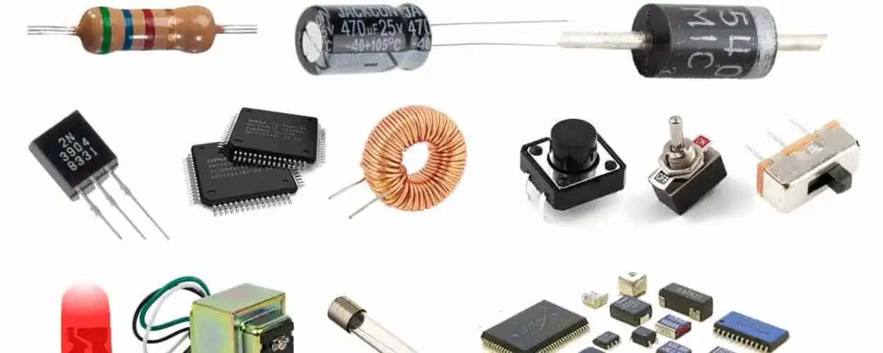
Main SMT Line Machine Efficiency 

The SMT line of PCB assembly contains the following few essential machines and equipment.

ยท       Pick & Place Machine

This P&P machine picks the SMT component and places it accurately over the surface of the PCB using the robotic placement hand. However, the tension in the surface of the solder pulls out the SMD automatically in alignment later in the soldering reflow process to fix little errors in the placement of the components.

ยท       Solder Paste Mixer

The soldering paste mixer, as the name suggests, mixes the paste of solder and powder efficiently and evenly. It helps in making the printing process, reflow, and standardized functions and minimizes the requirement of manual labor.

ยท       Oven

In the SMT line, both oven and reflow differ from each other. The oven bakes the PCBs to remove any type of moisture and comes in the last of an SMT line.

ยท       SMT Loader

The SMT loader places the circuit board in the soldering printing equipment racks automatically.

ยท       Solder Paste Printing Machine

The soldering paste printing device prints the soldering paste to draw off the board. It comes after the P&P device in an SMT Production line.

ยท       Solder Paste Inspection Machine

SPI refers to a Soldering Paste Inspection device. It analyzes the volume, thickness, and area of soldering paste over the surface of the PCB after the soldering printing process.

ยท       Reflow Machine

The reflow machine comes after the P&P machine. It melts the soldering paste between the SMT components and PCB to create a welding connection between them. After that, it cools down the solder paste and solidifies the welding bond.

ยท       AOI

The AOI machine sandwiches the reflow soldering machine in between two AOI. The first machine identifies any type of failures and errors in the placement of components before sending it to reflow. The second AOI checks the errors and failures of soldering after the reflow.

ยท       Docking Station

The docking station provides an intermediate stop between distinct machines of the SMT Production line.

ยท       SMT Unloader

The SMT unloader, as the name suggests, operates in the opposite way of the SMT loader. However, it receives the assembled board and stores it after the soldering reflow process.

Types Of SMT Production Line Efficiency

FULL PCB MANUFACTURING Quote

The design of the SMT line type contains the following details:

  1. One line contains a layout of a single rail P&P machine.
  2. The two-to-one line contains a layout of single or dual-rail P&P machine
  3. Tow-to-one contains the layout of a dual-rail P&P machine
  4. The three-to-one line contains a layout of a single-rail P&P machine
  5. Combination of multiple line layouts.

SMT Line Cost

SMT line contains around 60 to 70% pick and places robots. A large P&P machine that has a capacity of 100,000+CPH costs about $700,000. Whereas P&P with a middle range capacity of 12 to 35,000 CPH costs about $100 to $200,000.

However, the majority of brands usually cost one line of SMT of about $8,000,000. This seems so expensive. Therefore, we introduced high-tech, advanced SMT lines at a lower cost. It provides reliable and high-quality PCB production while keeping the production cost low. 


SMT Line Efficiency Development Trends

SMT production lines have several ongoing trends. Some of them include:

ยท       CIMS Application

CIMS refers to a computerized Incorporated manufacturing system. It basically links the production process and the design to minimize the time that preparation for SMT Production takes.

ยท       Efficiency Improvement

Efficiency is considered as the source of high output. At the same time, SMT lines are continuously obsoleting the human factor. However, to improve efficiency, try to implement a centralized CMS for the whole SMT line.

ยท       Environmental Protection

SMT production lines use materials like glue, solder paste, flux, and packaging material, which lead to environmental pollution. Although, the majority of PCB assemblers and manufacturers have started using an eco-friendly production process. They first identify the source of pollution and analyze how much quantity they use in the process. Then they look for methods to minimize their effect on the surroundings and create an eco-friendly environment. 

ยท       Flexible Production Environment

Internet development and grid IT provide process data control along with data management of products. This improves the functions of SMT lines. Moreover, they help in increasing maintenance management. Thus, eventually, make a flexible data integration production setup for SMT production lines. 

Conclusion 

SMT lines play an important role in the assembly process of Printed Circuit Boards. These SMT lines contain various types of high-tech machines that perform different types of functions. This article has explained all the details that you might need to know regarding SMT production lines. However, if you still have any type of query. Feel free to contact us.

Choose Rayming PCB for Irregular component Soldering Service

Irregular component

Wave soldering is highly important for smooth PCB assemblies, and we all know that. The process is popular among producers due to its quality and benefits. It strongly develops connections between the PCB parts and PCBs so that no harmful and unfavorable conditions would detach the components from PCBs. Wave soldering works on waves that come after each other to connect the components. Wave soldering is an interesting process, and we are going to explain our services besides wave soldering in this post so that you can choose what fits best for you easily!

As you already know, a PCB has a wide range of multiple components. Some are big, while others are small. You need a seasoned firm that can manage and assemble these components for your PCBs so that you can benefit from PCBs in the long run. We can help you with this. Our PCB assembly services have satisfied several customers like you. Our team of experts will address all your PCB-related problems and makes flawless assemblies possible for you. We offer services like BGA assembly to help you with all the issues so that it can save you time and energy. 

Below we are going to discuss some important factors that play an important role in PCB assemblies. Without these, PCBs might fail to perform effectively, leading to damage as well. So letโ€™s see the factors this instant:

Connectors & Contacts

PCB board to board connector
  • You might know that pin headers are a common part of PCBs, and these are available in different types. However, this is not the case with all PCBs.
  • Connectors are also important for some particular PCBs to function properly. These offer smooth interfaces that add to the delivery of PCBs for electronics. 
  • Other than this, you can go with coaxial and UFL connectors as per your project.
  • We know that connectors play a huge role in PCB assemblies, and this is why we have trained our experts to work out such connectors for your PCBs.
  • Not just this, but we are able to produce appropriate connectors for your PCBs at the same time. Our technicians just need important data and instructions from your end, which will get you desired connectors.
  • Not to forget contacts for PCBs assemblies, and you can rely on them on us completely. Hereโ€™s why: Spring-loaded contacts are regular types that we mostly work on. These are important for your high-frequency devices and RF machines. Sometimes these can wear out and need a quick replacement. You can have them quickly replaced by consulting our technicians, as they will come soon and serve you without any complications. 

Press-Fit Parts

  • These are an exception when we discuss PCB assemblies. Many producers fail to understand that press-fit parts need a special method for assembly, like wave soldering and reflow soldering. Due to this reason, you need seasoned assistance from us to work on press-fit parts. 
  • You need plated holes for these so that they can restrict the tolerance which follows through-hole assembly. We can efficiently work with this so that you don’t have to face any issues with that later. 

Modules

  • Modules are ICs and microprocessors that are important parts of several electronic devices. 
  • These are mostly present on congested PCB surfaced in general cases. 
  • Modules are crucial for high-frequency machines and RF equipment. 
  • You need precise castellated holes for the modules so that they can secure their position at the periphery of PCBs. 
  • In special cases, gold fingers will do the job if you just use the through-hole method. 
  • We specialize in dealing with modules for you and never compromise on effective management as well. 
  • However, if your modules don’t meet our DFA restrictions, we won’t be able to help you out. 
  • Module packages are not similar to PCBs in terms of assemblies; instead, you will consider them like normal SMT components

Part-On-Part (POP) Assembly

  • Our other service is POP assembly which can save your day from hustling for your PCBs if you hire us. 
  • So what is POP? It is the latest tech regarding PCBs which stacks some special components during assembly.
  • It comes in handy when you are aiming for miniaturization and optimizing the PCB surfaces. 
  • The primary benefit of POP is the HDI of the PCBs which makes them more efficient to work for heavy-duty machines. 
  • The components also gather less space when we work with POP-type assembly and benefit applications like microprocessors used in PCs. 
  • Our experts are adept in POP assembly no matter what type of PCB you will have for us. 
  • You can consult our active customer support to consult our technicians for POP assembly and get started with your PCB as soon as possible. 

Problem Packages

  • We know some packages can be problematic, but our expert engineers and technicians are the best problem solvers. 
  • However, we still do not work for some of the packages as they don’t fall under our expertise and guidelines. 
  • Speaking of which, we are offering semiconductor die assembly services to our customers since such packages are normally delicate and need special professional supervision to avoid complications.
  • The die needs our special attention here, especially when we are handling packages like QFP, BGA, and SOIC
  • The die is the element that complicates the assembly process, and for this, you need experts like us to cope with a problem package. 

Types of Soldering Defects

FULL PCB MANUFACTURING Quote

Disturbed Joint

  • An experienced PCB firm is one that can address major soldering problems for its clients. The disturbed joint is one of them, and we are going to discuss how our experts handle disturbed joints during soldering. 
  • Disturbed joints are like flakes and irregular chunks that are visible during soldering. When you are not applying the solder properly, it will develop a disturbed joint. Consider it just an accumulation of the solder on the PCB surface. 
  • Nonstable PCB surfaces also contribute to developing disturbed joints that negatively impact the composition. 
  • So it means there should be no oscillations and mishandling when you are dealing with the solder. These are also similar to cold joints; however, their causes are hugely different. 
  • So how do we address the disturbed joints? We will heat them and wait so that they will get solid again. 

Untrimmed Leads

  • Untrimmed leads are fatal, and we don’t recommend you deal with them on your own without professional assistance. 
  • These are visible with the solder joints and look like little spikes protruding out of the system. 
  • If two or more untrimmed leads interact with each other, they will cause a short circuit which means electrical fire and current leakage are also more likely to happen. 
  • So in this dangerous situation, you need to consult us before making any decisions. 
  • We will have our experts address this problem as soon as possible by re-trimming the spiky ends of these leads. They will re-size the leads and assemble them in an accurate position so that they will not cause any more damage to you. 

Solder Bridge

  • It usually happens when you are using excessive solder, and it accumulates between the solder joints of PCBs. 
  • It can mangle the PCB on the whole since the amount of solder is way more than sufficient. 
  • You can eventually make your board useless if the two joints of the PCBs interact and combine together due to the application of solder in them. 

Lifted Pads

  • Lifted pads are also a common defect when we are doing the assembly. 
  • Sometimes spots and sometimes pads can complicate the smooth PCB assemblies. 
  • Lifted pads also develop when you mishandle the hot iron in the joints of the PCBs, which will make your board dysfunctional. 

Stray Solder

  • Stray solder is also a common issue that most users like you face. Some remains of the solder left on the PCB can interfere with natural soldering.
  • These never combine with the copper wires and also damage the flux, which will reduce the efficiency of PCBs. Therefore make sure to clean your PCBs so that there will be no residue of solder. 

Insufficient Wetting for the Pin

  • Insufficient wetting of the pin can also create problems for you. It does not let you heat the pin properly, which resists the solder from properly covering the area and getting into place as well. 
  • It means you need to be careful while heating the pin. Make sure you are giving adequate heat to the pins to avoid insufficient pin-wetting. 

Conclusion

You can face any trouble with PCBs at any time, and it can be fatal for you if you decide to handle these problems on your own singlehandedly. That is why you need professionals to help you out with this. We are hopeful that after reading this discussion, you will be able to give our services a try so that our technicians can help you with their expertise and extensive engineering skills to solve soldering effects for you. Also, you never go wrong with our PCB assembly services and wave soldering expertise to outshine your PCBs on the whole. 

What are the Types and Functions of WiFi Antenna?

WiFi Antenna

Wireless local area networks (WLAN) require antennas for their functioning. These antennas are responsible for the wireless signal used in browsing the internet, playing games online, and other activities that require internet connection. The world we are in today is a digital one. Therefore, the internet plays a crucial role in our daily activities. Both businesses and individuals need the internet to carry out some of their activities.

Electronic devices such as computers, smartphones, and televisions can communicate with each other through WiFi. Connecting more devices can result in some certain issues like weak WiFi signal. WiFi has made it much easier to connect with the internet. These days, people now find it very easy to connect several devices to the internet via WiFi.

What do WiFi Antennas do?

Wireless devices can communicate with one another by using RF waves.  These devices include smartphones and routers. They comprise transmitting and receiving antennas.  WiFi receiving antennas transform electromagnetic waves into electrical signals while the transmitting antennas do the reverse.

Furthermore, a WiFi antenna offers an improved performance and better range when walls or other form of barrier blocks signals. WiFi is a short-distance wireless communication system that develops local networks. Its signals can get to 15 Km over 9 miles if they have got the right antenna. This means that Wifi signals have the capability to pass through isolated places or thin walls. However, they canโ€™t pass through stands of trees or big buildings.

What are the Types of WiFi Antennas?

2.4G WiFi Antenna
2.4G WiFi Antenna

WiFi antennas are of two main types which are directional and omnidirectional.

Directional antennas

These antennas concentrate all of power in just a single direction. They function in a similar way as a flashlight. For example, when a flashlight is switched on, it radiates the space you shine its light. The beam width of this flashlight is in a triangular shape. Therefore, any item outside the triangle wonโ€™t get light.

Directional antennas can transmit and receive wireless signal from a far distance. This is because the power of these antennas is in one direction. However, they have a small coverage area. This means the light can go beyond one room. However, it wonโ€™t radiate a whole room. You can use directional antennas for long-range point to point networks to enable internet connection between buildings.

There are different classifications of directional antennas. These include:

Mini panel antennas

These antennas can transfer radio waves from a particular area to a certain area. Mini panel antennas can enhance WiFi signal indoors. Also, they can be used instead of a paddle antenna on a router. These antennas need to be focused in the direction where you would be transferring a signal to and get a signal from. This helps to get rid of any connectivity problem that may likely occur. Also, you need to understand that the radiation patterns of mini panel antennas are 60 degrees.

Yagi antennas

This type of directional antenna looks like arrows. A Yagi antenna can only function when it focuses in the direction it is transmitting a signal to or getting a signal. The radiation pattern of a Yagi antenna is 450.

Panel antennas

These are very powerful antennas that enable signal transmission from very far distances. You can link them to a router for further transmission of data or connect them to a USB WiFi adapter to get data from far distances. These antennas are usually more directional when compared to mini panel antennas. Also, panel antennas feature a radiation pattern of 35 degrees.

Omnidirectional antennas

These are the second type of WiFi antenna. They transmit a signal at a 3600 angle in order to offer the most broad signal coverage. Omnidirectional antennas are similar to un-shaped incandescent lightbulb. For instance, a lightbulb will disperse light evenly in every direction in order to provide illumination to a room.

The range of omni-directional antenna is much shorter than that of a directional antenna. However, omnidirectional ย antennas have a much larger coverage area compared to directional antennas. This means the light radiated by the lightbulb wonโ€™t go any further as that of a directional antenna. You can use omnidirectional antennas in outdoors and indoors.

Classifications of Omnidirectional WiFi Antennas

There are different classes of omnidirectional WiFi antennas.

Outdoor omni antennas: These antennas can enhance WiFi signal when used outdoors. When these antennas are linked to a router or an outdoor access point, they enhance the wireless coverage outside.

Paddle or dipole antennas: They are usually integrated in WiFi adapters, access points, and routers.

Ceiling dome antennas: You can connect these antennas to an access point or WiFi router through coaxial cable. Based on their name, these antennas are installed on the ceiling of homes. Also, they are found in warehouse or office building.

The Wavelengths, Frequencies, and Range of WiFi Antennas

FULL PCB MANUFACTURING Quote

WiFi devices need radio waves to interact with each other. Just like all other waves, frequencies are the measurement of radio waves. These frequencies are the Hertz per second that is transmitted and received within a particular interval. It should be noted that WiFi antennas integrate several frequencies when transmitting data. These frequencies are 3.6 GHz, 5 GHz, 2.4GHz,  4.9 GHz, 900 MHz, and more. The frequencies specifically range from 900 MHZ to 60 GHz.

5GHz and 2.4 GHz are the two highly preferred frequencies utilized in WiFi communication. These frequencies correspond to wavelengths of 6cm and 12.5 cm. Based on this information, you will realize that lower frequency waves usually have longer wavelengths. Therefore, WiFi antennas with lower frequencies find it very easy to pass through obstacles like walls and metals. This enables them to transmit data further. However, data transfer is usually at a very slow rate.

On the other side, shorter wavelengths move at a faster rate and as such, this allows the transmission of very high speed data. But, shorter wavelengths find it very difficult to penetrate obstacles which in the long run, minimize the range of the signal.

WiFi antennas are carefully designed to correspond with the wavelength and frequency of the signal being transferred. This means that, a 2.4GHz antenna can never replace an antenna of 5GHz and vice versa. Also, some WIFi antennas can use both frequencies. These antennas are often referred to as dual band antennas. They have the capability to function under one frequency at the same time.

What are 5GHz WiFi Antennas?

5GHz WiFi antennas have a much shorter range coverage. However, this is much higher than 2.4GHz antenna. Also, the penetrating power of this antenna is less. It finds it difficult to pass through objects such as walls. The 5GHz frequencies are integrated in W-Lan and WiFi applications.

What is WiFi Antenna Gain?

Gain measures the ability and strength of an antenna and how it can direct EM waves in a particular direction. Decibels (dB) represent the measurement of antenna gain. Isotropic antennas feature 0 gain or O dBi. These antennas transfer and receive an even signal in every direction.

Antennas that feature much higher dBi measurements can reach further and stronger. Therefore, they are believed to be a much better option. However, antennas with higher dBi arenโ€™t usually better. The range of these antennas increases as their dBi rises. However, there is a decrease in their coverage area.

Letโ€™s say an isotropic antenna is like a symmetrical ball. The sides of this ball will increase once you press down. The ball will become flatter when you add more pressure to it. Also, the ballโ€™s beamwidth will be altered when you add gain. Therefore, this changes the shape of the ball from a sphere to that of a pancake.

Importance of WiFi Antennas in Homes, Offices, and Outdoor Spaces

Improves WiFi Signal at home

WiFi antennas can improve WiFI signals, enabling them to get to dead zones. When used in the home, these antennas improve the performance of your WiFi signals. The best way to enhance the network in your home is to move the antenna to a central location. If there are dead zones in your home, there are some antennas that can help you enhance the coverage.

For instance, if your home has a wireless gateway with no detachable antennas, an Ethernet cord is a great option in linking the gateway to a wireless router without detachable antennas.

Enhance WiFi signal in offices

Offices or commercial spaces are usually much bigger than homes. In some cases, there are obstacles that prevent WiFi signals from penetrating. Just like our homes, we always want the antenna to be in the best location. Luckily, if the router features detachable antennas, it could help in enhancing the coverage.

Office buildings have different devices positioned in different areas. Devices such as laptops, computers, cell phones, and printers are best used with omnidirectional antennas. It is possible to enhance the signal in big spaces with ceiling dome antennas. You can install these antennas on a buildingโ€™s ceiling.

Boost WiFi Signal outdoors

In most cases, WiFi signals donโ€™t always have a high transmission rate outside since there are hindrances that weaken the signal. An outdoor omnidirectional antenna can be a great tool in boosting the WiFi signal in outdoor spaces. This antenna offers a better signal when used. You can connect it to the router or an access point outside.

It is advisable to get a low gain antenna for outdoor spaces. This is because this antenna offers the best possible coverage. ย High gain antennas can discharge signal at farther distances.

What Does the 5.8GHz Antenna Offer?

The 5.8GHz antenna is a dual-band WiFi antenna that supports about 1300 mps. This antenna is commonly used since it offers enough frequency needed to allow modern wideband signals function. Also, this antenna is affordable and more economical.

You can improve the quality and range of a wireless connection by using this antenna. 5.8GHz antenna offers higher frequency than 2.4 GHz antenna. Most devices used in homes run on the 2.4 GHz antenna. However, the 5.8GHz band has less overcrowding compared to the 2.4GHz. This is because there are fewer devices that integrate this band.

There are 23 different channels in the 5.8GHz antenna and devices can integrate these channels. Meanwhile the 2.4GHz band features 11 channels and this depends on your regionโ€™s wireless regulations. 5.8GHz antennas offer less coverage. However, these antennas offer faster data transmission.

What to Consider When Choosing the Best WiFi Antenna

Size

Speaking of connectivity, the size of a WiFi antenna matters a lot. A big antenna can enhance your signal range and offer more reliable signal.

WiFi signal direction

This usually indicates the antenna type you need. A directional antenna will be ideal if you need to link one or more machines in the same direction.  However, if the devices you intend to connect are in different location in a building, you should opt for an omnidirectional WiFi antenna. There are a wide selection of WiFi antennas and you can choose based on your choice.

Interference

In this case, you have to consider the interruption your WiFi signal may experience. Physical obstacles and interruption are two different things. Also, interference attacks signals and minimizes their strength or blocks off the signal completely. Therefore, you need to choose a WiFi antenna that can tolerate this interference.

Range

Distance, obstacles, output, and power are factors that could weaken the signal of a router. Physical obstacles could be in houses or furniture. If you are purchasing a WiFi antenna, put these obstacles in mid.  Opt for an antenna that can intensify a signal regardless of the obstacles.

Cost

People donโ€™t often consider this when choosing a WiFi antenna. Cost usually determines everything in the long run. Although you shouldnโ€™t compromise quality or functionality for cost, there are budget-friendly antennas out there.

Conclusion

WiFi signals can go out of reach across cables. Therefore, integrate the minimum length of the cable. WiFi antennas with higher gain are ideal for signal transmission over long distances. To get the best WiFi signal, ensure the polarization between antennas corresponds. WiFI antennas are integral part of a wireless connectivity. Every WiFi antenna has receiving and transmitting properties that influence the coverage area of a device.

How Exactly Does a Cellular Antenna Boost Network Reception?

Cellular Antenna

Telecommunication has made it possible for us to keep in touch with loved ones, have access to the Internet and basically do anything we can to be updated with what goes on around the world.

A bulk of the success of telecommunications relies on the excellent performance of the telecommunication providerโ€™s network. You might have experienced disturbances while on a call, such as the line going off or the network breaking. If that has been the case, there is one logical explanation โ€“ your device doesnโ€™t have enough network.

In such cases, you want to go for a cellular antenna, otherwise called a network booster. In this article, we explain how the antenna works, some of the benefits and the different options available for you to choose.

What is a Cellular Antenna?

The simplest explanation is that it is an antenna that is meant for use with cellular devices. To put it into perspective, you need the antenna to boost the telecommunication network that comes into your cell phone.

How Does an Antenna Work?

To have a better understanding of the operations of a cellular antenna, we would like to explain the basic concept โ€“ antenna. Here are some of the things you need to know:

  • Antennas enable the conversion of radio waves into electric power and vice-versa.
  • The antenna works hand-in-hand with the radio receiver. For this to work, the antenna has to receive the oscillating radio frequency electric current from the radio receiver. This is receiver in the antennaโ€™s terminals and sets the stage for the antenna to radiate the energy derived from the current as electromagnetic waves.

When it comes to signal reception, the antenna works by intercepting some of the electromagnetic waves. Once this is done, tiny voltages will be produced at the terminals and these will be used to amplify the waves at the radio receiver/transmitter.

Do I Need a Cellular Antenna?

More often than not, you would make do with a cellular antenna, but you need to be sure you need it.

Here are some reasons why getting a high-gain cellular antenna is a good move:

  • Signal Amplification: you need the antenna to help the cellular phoneโ€™s built-in antenna to receive better signals. This need is necessitated by the fact that there might just not be enough signals outdoors. In this case, there wouldnโ€™t be enough either to deliver indoors.
  • Data Rate Improvement: cellular antennas can also improve the speed of your networkโ€™s data. This works best if you are looking for a higher Megabyte per Second (Mbps) download speed.
  • Long-Range Connections: you need to get a long-range cellular antenna to help you connect multiple devices across a longer range.

What is the Importance of Cellular Antenna?

Besides the signal boosting capabilities, the cellular antenna can also provide a couple of other benefits. Here are some of the additional benefits:

Cellular Antennas are Reliable

Certain factors are responsible for the limited signal you get on your device. If it is not the farther distance of the cell site/tower, it would be the presence of obstructions, such as an exterior wall.

Whichever is the case, the fact is that the network coming into the home or office from the outdoors might not be strong enough. Getting a cellular antenna to compliment works fine, as it helps you get guaranteed coverage.

Improved Data Performance

Do you notice that your Internet connectivity becomes sharper and faster when your Wi-Fi router is close? Such is the experience when you get a cellular antenna โ€“ your data transfer speed will significantly improve.

Long-Range Connection Capabilities

The demand for wireless cellular networks that connect over longer distances fuels the increasing popularity of cellular antennas.

The capabilities of these antennas towards connecting devices over larger distances are impressive. For example, you can rely on the 5G antenna to provide a larger bandwidth per unit area for applications across different industries.

Cellular Antennas & Cellular Signals

The trend of 5G networks didnโ€™t come about. It is a record of the impressive successes to the previous generations of cellular signals, such as 2G, 3G, 4G and now talks of 6G are already rife.

The success of cellular antennas relies on the type of cellular signals they are to be used. As a rule of thumb, these antennas must be used with the right cellular signals to avoid the primary problems they wanted to solve โ€“ the inability to get reliable signals.

We will now go in-depth to talk about the different types of cellular signals.

3G Antenna

This refers to the third generation of wireless telecommunication technology. Some of the highpoints of 3G cellular network include:

  • Simultaneous Cellular Network Usage: the 3G technology supports the dual usage of the signal both for data transfers and voice telecommunications.
  • Local Connection Enhancements: 3G networks also support the localization of cellular signals, such as the usage of devices on local wireless networks. It also supports the enhancement of the local Internetโ€™s signal strength.

The Types of 3G Antennas

There are different kinds of antennas you can use for your 3G network. They range from directional, omni-directional and clip antennas.

Here is a summary of how each works:

  • Directional 3G Antennas: these antennas are pointed in the direction of the cell site/tower. The aim is to get better signal and supply the same to the cellular device.
  • Omni-Directional: unlike the former, the omni-directional 3G antenna doesnโ€™t necessarily need to derive signals from the cellular tower. Instead, it can pick up these signals from any direction.
  • Clip 3G Antenna: this type of 3G antenna is designed for mobility purposes. You can clip or attach it to your device (laptop or computer)โ€™s screen for better signal reception.
  • Outdoor 3G Antenna: this type of cellular antenna is meant for locations or areas with limited indoor cellular signal. By mounting the antenna outside, you get to receive better signals indoors.
  • High-Gain Cellular Antenna:ย this is one of the 3G antennas and its primary use is for boosting the (Internet/data) signal for areas with limited data coverage.

Advantages of 3G Antennas

FULL PCB MANUFACTURING Quote

Cellular antennas designed for use with 3G networks are useful in the following ways:

  • The antenna provides high-speed access to both data transfer systems and cellular phones.
  • It improves data reception and transfer rates for supported devices, such as telephones, computers and laptops.
  • 3G antennas reduce signal noise.

4G Antenna

The fourth generation of wireless technology comes behind the 3G antenna. One of the major reasons for developing the 4G network was to bolster Internet connectivity.

However, this comes with some considerations, such as being close to a โ€œ4G areaโ€ to access the 4G network.

The Role of MIMO in 4G Networks

Multiple Input Multiple Output (MIMO) is one important feature of the 4G wireless technology. It functions as a slant polarizer for the electromagnetic waves. This plays an important role in the derivation of faster Internet speeds via the use of two separate antennas.

Types of 4G Cellular Antennas

There are two primary types of cellular antennas you can use to boost Internet speeds for your 4G device.

Here they are:

  • High-Gain Antennas: this type of 4G cellular antenna supports the delivery of Internet-enabled signals across longer distances. You however want to take note of the fact that the data speed might be reduced, as more users access the 4G bandwidth.
  • Multiband Antennas: these antennas also provide reliable data transfer rates across longer distances. They also increase the operating bandwidth.

5G Cellular Antenna

This is one of the cellular antenna types, but it is a step-up to the 4G network. The 5G wireless technology can provide data transfer rates of up to 1 Gbps.

Types of 5G Antennas

The following are some of the antennas you can use with 5G devices:

  • MIMO: this refers to the Massive Multiple Input Multiple Output (MIMO) antenna that uses the 5G NR architecture to support the MIMO capabilities for multiple users.
  • PIFA 5G Antenna: this is the Planar Inverted-F Antenna (PIFA) antenna that provides omnidirectional radiation and reduces the number of bits a smartphone uses.
  • Fractal Antenna: this 5G antenna improves the outside structure or internal componentsโ€™ circumferential. It achieves this via the use of a recursive, identity system.

Challenges with 5G Antennas

Using 5G antennas to boost Internet connections and data transmission speeds can pose some difficulties. Here are some of the challenges to the usage:

  • The MIMO functionality on the antennas often require a synchronization of different antennas. This synchronization must be done on a device that uses a similar frequency band.
  • The 5G (small cell) antennas are commonly used to fix and relay cellular signals. They are also used for distribute these signals in denser packages. This is the reason why the non-obstructive properties and compactness of the antennas must be a priority.

6G Antennas

The success of the fifth generation of wireless technology paves the way for the sixth generation. The 6G technology is expected to introduce a couple of innovations, chief among which is the delivery of higher frequencies than the 5G network provided.

In a publication, Popular Mechanics hinted that the 6G wireless technology may use the โ€œhuman being.โ€ The publication cited a report by a team of researchers at the University of Massachusetts who suggested leveraging the use of human-worn coiled copper and a Visible Light Communication (VLC) system to โ€œharvest waste energyโ€ for fostering the performance of the 6G technology.

The following are some of the things you need to know about how 6G antennas are poised to fuel the next-generation of wireless technology:

  • High-performance vertical and horizontal interconnections, as well as feed networks will be facilitated by the following: Antenna-in-Package (AiP), reduced signal integrity and on-chip antenna technologies.
  • Sub-THz communication will leverage relevant innovations, such as metasurface-based antennas, massive antenna arrays, and lens antennas.

Cellular Antenna Buying Guide

Looking to buy a long range cellular antenna? Here are some of the factors you want to consider before making that purchase:

1. What Material is the Building Made of?

Whether you are using the antenna at home or at the office, you want to make sure that the signal doesnโ€™t get interrupted.

The type of material used for the building can influence the rate of transmitting the signal inside. As a rule of thumb, the signal waves can be blocked if the building material comprise any of the following: brick, wood, drywall or glass.

2. Determine the Best Cellular Antenna Types

The indoor and outdoor cellular antenna types are the most common. While the former is used inside the home or office, the latter is best used outside.

When it comes to this, let us see how they compare:

  • Indoor Antennas: these are either panel antennas or dome antennas. The panel antennas are best for transmitting cellular signals across multiple floors, while the dome indoor antennas are best for one floor in the building.
  • Outdoor Antennas: here, you get to choose between the directional and omni-directional outdoor antennas. While the former gets signals from one direction, the latter initiates a 360-degree search to pick up working cellular signals from multiple directions.

3. Be Certain of the Coverage

The size of the area to be covered is also important. The general rule is to go for a cellular antenna that can cover the length and breadth of the area where you intend to use it.

4. How Many Users are to be Connected?

As much as the cellular antenna can draw in more signals, it could also be impeded at some point. The number of users connected to the antenna or booster could potentially reduce the data and signal transmission speed.

5. The Incoming Signal Matters

The strength of the signal coming from outside the building is very important. It is important to note that this works best for indoor antennas. In this case, the outdoor antennas need to connect to the cell site/tower so that it could derive the cellular signal. Once obtained, the signal is sent to the amplifier, from where it is enhanced ahead of the transmission to the cellular antenna for rebroadcasting.

Wrapping Up

RayPCB can help you evaluate the numerous options so you can have a clear-cut idea of the best cellular antennas to get for your home or office usage.

Differentiating between Conductive vs Non-conductive Via Fill PCB

Via in PCB

Do you know that a via needs to be filled? After it has been used to establish a connection between the circuitโ€™s layers, you have to get them filled. In this article, we help you understand the two major ways to get this done.

What is a Via?

It is the copper plated through-hole primarily used for connecting multiple (two or more) layers in a Printed Circuit Board (PCB).

What is a Via Fill?

It simply refers to the filling or closure of the via. It is important to mention that the filling or covering process is important, as it improves the reliability of the connections.

Thus, you need to use any of the common via fill processes to close the viaโ€™s holes.

What to Use for Via Fill?

It is common to use epoxy for covering the via holes. The choice of epoxy for the process is borne out of the fact that the material supports the retention of the solder at the assembly level. This allows for the reduced risk of compromising the solder joints and to keep away the bath solution from the surface.

Via-in-Pad vs. Through-Hole Technology

Today, you can choose between the through-hole technology and via-in-pad for filling the via in a PCB.

It is best to stick to using the via-in-pad process as compared to the through-hole process. The benefits to using it include:

Routing Density Improvement

The routing density (when measured in terms of the higher density per layer), is improved.

Streamlined Signal Transfer Process

The via-in-pad process also streamlines the process of transferring the signals. It is evident in the streamlined method of filling, planarizing and plating the via over copper. This proves to be a better method when compared to the traditional process of transferring the signal from the Ball Grid Array (BGA), pass it through the via and then have it passed on to the inner layers.

Additional benefits of using the via filling process are:

  • Reduction of the circuit boardโ€™s size, as well as the number of layers used therein.
  • The filled vis process also does away with the high-speed design constraints, especially low inductances.
  • It strengthens the padโ€™s attachments.
  • Filled vias also reduction the EMIs.
  • Increased thermal and electrical conductivity.
  • Through the use of filled vias, the high-frequency designs will have shorter possible routes, for bypassing the capacitors.

What is Conductive Via Filling?

It is one of the via fill processes/options for circuit boards. It refers to the process of initiating a transfer of electrical signals from one part of the PCB to the other. At the same time, the viaโ€™s thermal transfer properties are improved, while enabling the electrical signal transfer.

Conductive Via Filling Materials

You can choose between copper and silver epoxy for this purpose. The major advantage to the two is the excellent thermal conducting property. For example, you can rely on these materials to do the following:

  • The improved heat/thermal conductivity is accentuated by the metallic design of the via fill. This sees to the excellent transfer of heat from the Integrated Circuit (IC) to the other side of the PCB.
  • Once the heat is dissipated to the PCBโ€™s side, it is further moved away via the heatsink.

The major materials used here are the DuPont CB100 and the Tatsuto AE3030 epoxy fill. With the two making up the โ€œsilver coated copper particleโ€ and filled with the epoxy matrix; they are ideal for the improved thermal and electrical conductivities, even in a cured state.

Here are some of the additional points to note about these materials:

  • CTE Differences: there is a difference between the Tatsuto AE3030 and DuPont CB100, based on the Coefficient of Thermal Expansion (CTE). This difference is based primarily on the CB100โ€™s longer usage and the fact that it comprises both a higher CTE and a larger particle size.
  • The silver epoxy is used mostly and quite affordable, when compared to the superior heat conductivity capabilities of the copper conductive epoxy.
  • The use of a conductive polymer layer deposition method significantly the flow of current between the internal layers and vias of the circuit board. This is derived via the deposition methodโ€™s placement on the PCBโ€™s via-hole.
  • It is also possible to save up on costs via the conductive polymer layer deposition method. This can be enhanced via the direct metallization of the via holeโ€™s inner walls.

What is Non-Conductive Via Fill?

FULL PCB MANUFACTURING Quote

This process is not entirely an opposite of the conductive via fill option, because it is processed the same way as the latter.

However, the difference between the non-conductive via fill and the conductive via fill is based on the purpose. While the non-conductive is used for preventing the contamination of the via by solder and other contaminants; the conductive option allows for the effecting both signal and heat transfer.

Here are some of the additional benefits of the non-conductive via fill process:

  • The plating of the vias also supports the conduction of electrical signals and heat.
  • Non-conductive via fills also see to the creation of a structural support for the copper pad that covers the holes.

Non-Conductive Via Fill Materials

Both Peters PP2795 and San-Ei Kagaku PHP-900 epoxy are the common materials used for non-conductive via fills. The former has been enjoying the many years of usage, but now has a fierce competition in San-Ei, which has become a popular choice in recent years.

Conductive vs. Non-Conductive Via Fill Differences

The first difference between the two is that the conductive via fill facilitates the transfer of electrical signals and heat, while the non-conductive via fill primarily prevents contaminants from getting into the via.

Depending on the PCB designer and targeted application, using the non-conductive via fill option might be better. These reasons support the claim:

  • Solder Bridging Prevention: the risks of solder bridging are greatly reduced due to the stoppage of the solder mask on the filled vias a few mils short of the pad. When used in the medium-density circuit boards, it helps to prevent solder bridging between the nearby pad and the via.
  • The fill materials for the non-conductive vias help to fill the gap that contained air before.

CTE Value Matching

You also need to match the value of the Coefficient of Thermal Expansion (CTE), as it pertains to the via filling to be applied. This matching is important because of the reduced risks of stress-related fractures. These fractures are commonly caused by the contraction or expansion triggered by the same circumstances.

Here are some of the steps involved in the CTE value matching:

CTE & Surrounding Laminate

The first value matching should be between the surrounding laminate material and the Coefficient of Thermal Expansion (CTE).

This comes in handy as the circuit board โ€œlives off the lifeโ€ in an on/off and heating/cooling state of expansion and contraction of the padstack structures.

Between Conductive and Non-Conductive Epoxies

Should you choose the conductive epoxy or go for the non-conductive variant? Generally, the non-conductive variants are a better bet for the CTEโ€™s value matching. This is because they provide a more reliable overall structure for matching the CTE to the laminate.

On the other hand, despite the widespread adoption of the non-conductive epoxy; the conductive variant can also be used.

Considering the popularity of the DuPont CB100 as the best via fill, it is evident why the conductive epoxies are still popular in some quarters.

The following reasons also support the necessity of using the conductive epoxies for CTEโ€™s value matching to laminate:

  • Conductive epoxies are ideal for use with the high pin count Ball Grid Arrays (BGAs), especially the ones that โ€œrun hot.โ€
  • Conductive epoxies are a better option for the thermal vias. These vias benefit from the epoxiesโ€™ capability of fast-tracking thermal energy out and away from the originating source.
  • Legacy or older electronic products also benefit from conductive epoxies. The usage is due to the long-standing popularity and improved lifecycle properties.

Away from Conductive and Non-Conductive Via Fills

vias on pads
vias on pads

It is common for the non-conductive and the conductive via fills to be used in covering the vias in a PCB. However, there is a third option, which is not fully harnessed. The name is Copper-Plated Shut Filled Vias.

It is a filled vias process commonly used when the aspect ratio gets to 10:1. You can also use it when the diameter is less than 8 mils.

Considerations for the Copper-Plated Shut Filled Vias

It is imperative to mention that the copper-plated shut filled vias can also be prone to a couple of challenges. The following are some of the things you need to know:

  • If you are using either the Teflon or PTFE materials, rest assured that they would distort in the process.
  • Certain materials are better not used for the design. For example, thin materials or subs measuring less than 20 mils may not be ideal. This is because of the difficulty in processing through planarization. Besides, the material might be subject to tears or distortion.
  • The making of fine spaces or lines might not be possible. This is the case when wrap plating is required. It is a plating method that requires the termination of surfaces so they (the surfaces) could have a buildup of copper.

How to Manufacture the Filled Vias

Whether you are using conductive or non-conductive via fills, the processes often range from cleaning and preparation.

Here is a breakdown of the major steps that go into it:

1. Vias Drilling

You can choose between the laser beam and mechanical drilling methods for the viasโ€™ creation. You can determine the best viasโ€™ drilling method based on the number of circuit boards you want to produce, the costs and the hole depth.

Talking about the holes, make sure that the right annular ring size is created.

2. Clean the Vias

The drilling is followed by the cleaning process. The different cleaning options you can use are:

  • Brush and Solvent: this combination helps to get rid of debris, while paving the way for a smoother and finer drilling process.
  • You can also use a combination of chemical and abrasive mechanical processes for the cleaning.

Irrespective of the cleaning method used, one point to note is that the debris must be removed at all costs. Also, put the circuit board under close scrutiny to ensure that there is an even plating of the copper within the viaโ€™s holes.

3. Fill the Vias

Depending on what you want, you can choose to fill the vias with either the conductive or non-conductive via fill.

The via filling processes for a PCB include the filling of the holes with pressure and vacuum. This enables the excellent hole filling without giving a way for gap formation in the resin. The other process is to clean the panelโ€™s surface. This process serves a dual purpose of getting rid of the excessive resin and paving the way for planarization.

4. Planarize the Filled Vias

The planarization of filled vias refers to the mechanical-brushing process of getting rid of resin. It also requires the smoothening and flattening of the copperโ€™s surface. This way, a uniform surface is achieved, while getting rid of the excessive resin.

5. Over-Plating

This process comes after the planarization process is completed. Over-plating the PCB with copper is an ideal way of soldering the electronic components, accurately.

Before Filling the Vias

A VIA hole in a PCB

Note that despite the disparities between the conductive and non-conductive filled viasโ€™ processes; they also have some similarities and differences, which we have discussed in this article.

Generally, the processes of filling the via holes are fraught with some bottlenecks, which include:

  • Structure-related issues tend to come up.
  • There is a risk of filling up the via holes during the soldering process. If this happens, it tends to render the entire process useless.
  • Another challenge is choosing between the conductive and non-conductive via filling processes, based on the benefits they offer.

Final Thoughts

For the best results, always contact a professional PCB designer to help you navigate the hole drilling, soldering and filling process. Rayming Technology helps you make a perfect choice on which of the conductive vs non-conductive via fill PCB process is best for your circuits.

Exploring the Specifications and Applications of Temperature-Controlled Circuits

Temperature-Controlled Circuits

A digital circuit of temperature controller refers to a temperature control device that is used in home, medical, and industrial applications. This digital thermo controller seems better than a thermostat/analog system with poor accuracy. For instance, it proves helpful in devices like incubators where controlling an accurate amount of temperature is significant.

Digital Temperature-Controlled Circuits – Description of Block Diagram 

This refers to a digital thermo controller system that gives the data of temperature on the display. It switches off the load when the change in temperature starts exceeding the specific set point. Here we use a lamp for a load to give a demo explanation.

The digital thermo-controller system utilizes an 8051 series of microcontrollers. It serves as a heart or central part of the device. The unit of the display contains a four to seven parts display and a temperature sensor that interfaces with the microcontroller. The digital thermo-sensor interfaces with a microcontroller to sense the condition of temperature. Moreover, it also contains push buttons that help in adjusting the settings of the temperature.

The microcontroller, however, polls the data of temperature using a digital thermal sensor. It then displays it on the 7-part display. Therefore, when the temperature of the corresponding resistor rises from the specific set point, It automatically turns the lamp off.

How Does A Temperature-Controlled Circuit Switch Work?

Temperature-Controlled Schematic

A temperature or thermo control switch operates based on set values. Generally, it measures the environmental temperature and makes it a reference. Then measure the device temperature and compare both temperatures.

The sensor creates a power signal as an output as it completes its calculations. The output signal contains all the necessary variations. Moreover, the final element receives these output signals, which heat up or cool down the devices. Take an oven, a heater, a controller, and a thermocouple, for instance. The thermo-controller measures the temperature of the thermocouple of the oven and then compares them with a set threshold. Moreover, the Thermo controller also measures the run-time of the heater to maintain the environmental condition of the oven.

Temperature-Controlled Circuits – Relay Circuits

The temperature or thermo-controller circuit works and operates easily. One can easily create this temperature circuit. However, this simplicity does not affect its efficiency. In simple words, it proves ideal for almost all automatic thermal-control devices. 

This thermo-controller controls the integrated relay on the circuit. However, it uses a single-chip LM35DZ temperature sensor to commence this task. The relay begins working when the circuit temperature surpasses the set temperature. At the same time, it stops working when the circuit temperature starts going below the set point.

How Does Temperature-Controlled Circuit Work?

The temperature sensor LM35DZ serves as the central figure of the circuit. It uses the Celsius scale to work. At the same time, it uses a degree to convert the voltage to give accurate control. Moreover, the LM35DZ alters its power voltage output on the basis of the measured temperature. Also, its max temperature can range anywhere between 100 degrees to zero degrees Celsius.ย 

The preset VR1 and resistor R3 sets the temperature of a circuit ranging from 1.62 volts to 0 volts. Also, the op-amp reduces the voltage reference to stop the overloading of the R3 and V1. A comparator comes in. It compares the output voltage of LM35DZ with the set temperature. Additionally, it also determines whether to turn on or off the relay.

Applications of Temperature-Controlled Circuits

The output from the thermo-controller relay circuit can be used in cooling systems, heating systems, and alarm devices. For instance, the circuit helps in switching on or off the cooling fan when the circuit detects the change in temperature and reaches beyond the set temperature. Thus helping the heatsinks and semiconductor devices to cool down. Moreover, make sure to put the thermal sensor in a place that is close to the heating agents. 

Also, some other devices that need extra caution include outdoor usage, as it creates electrical interference and potential chemical connections. Also, systems like nuclear control devices, aviation devices, tailored devices, and combustion devices. Additionally, amusement machines and medical devices. Vehicles, safety equipment, and devices that need to be installed for industry and government regulations. Also, those devices, equipment, and systems that may affect the property or life need extra caution to install thermo-sensors.

Specifications of Temperature-Controlled Circuits

FULL PCB MANUFACTURING Quote

ยท Stability

It is hard to determine the stability of a system with a temperature controller, which serves as an essential specification. Thermistors are used to test the wavelength as it offers the greatest resistance to change at every degree Celsius. The load of the test is also controlled well using sensors nearby the device.

However, the thermoelectric, properly sized heat sink and all electrical components are connected with each other using high-quality thermal grease. It reduces the thermal resistance among them. Moreover, it gives stability in the form of Celsius and Kelvin. The range of typical stability can range below 0.001 degrees Celsius.

ยท Operating Temperature Range

Electrical devices contain a specific temperature range to operate well. It may lead to damage if the temperature exceeds or goes below that specific range. The wavelength specifies the device’s operating range.

It couples with the specification of Max’s internal dissipation of power. Moreover, when the value of the device temperature rises above the environmental temperature, the max internal dissipation of power drops to zero over the max operating temperature.

ยท Separate Monitor And Power Grounds

The temperature controller uses one higher power ground which connects with the supply of power. Various low-power grounds are present between the signals of the monitor to reduce inaccuracies and offsets. At the same time, high and low power ground connects internally and uses low power ground with a monitor to give the best results.

ยท Thermal Runaway

One thing that you need to understand is that when a thermoelectric removes the heat from a specific device, then heat needs to dissipate completely off the system. Moreover, any extra heat from overwork or inefficiency of components in a thermoelectric also needs to dissipate. Therefore, it needs an appropriate heat sink design.

It helps dissipate enough heat from the device and retains the temperature of the device below the surrounding temperature. But however, if the design does not suit well, instead of dissipating heat, it remains in a load. It, in fact, increases the temperature of the sensor rather than remaining at a specified temperature. However, a temperature control comes in, which drives additional cooling current from the thermoelectric.

Conclusion

A temperature controller circuit helps in controlling the temperature-sensitive device automatically. It operates without disturbing anyone. It also helps in avoiding various temperature effects. Moreover, it costs less, requires easy construction, and easily-available components. Thus making it ideal to use as a heat sensor.

A Closer Look at the Basics of Capacitive Circuits

capacitive circuit

An actual capacitor circuit refers to a type of circuit that comprises a pure and actual capacitor along with the C farads capacitance. The capacitor capacitance is a type of effect that occurs on strong electrical current in an electric field. It also serves as a condenser. It contains a dielectric substrate that separates both conductive plates and creates a capacitor. This dielectric substrate comprises mica, oxide layers, paper, glass, and other materials. Moreover, the current in the AC capacitor conducts the voltage at the right 90 degrees.

What Are Capacitive Circuits?

When the voltage passes through the plates of the capacitor, it creates an electric field around it. However, the current does not follow them. However, when an inconsistent voltage source device connects across the plates of a capacitor, the discharging and charging of a capacitor flow the current through the voltage source.

Definition Of Capacitive Circuits

A capacitor consists of two plates of dielectric material that separate from each other through the dielectric source. The capacitor stores the electrical energy in them. Thus reacting as a medium storage application. It charges when the device power turns on and discharges when the device power turns off. The charging directly connects to the voltage applied to it when connected to a power supply directly.ย 

How Capacitive Circuits Behave In Alternative Current Circuits?

Choose a large capacitor or a small capacitor

The capacitor behaves and reacts differently when an Alternating Current applies to it. Capacitors operate differently from resistors. Resistors allow electrons to flow through them, which are directly rational to the drop in voltage. At the same time, the capacitor does the opposite of it. It does not allow the voltage to drop. In fact, when the current is supplied to it, it charges or discharges the current into a new level of voltage. 

In a direct current supply, when the voltage supply remains constant, the capacitor starts charging up to the supplied voltage value. Where it acts as a storage device and stores the charge indefinitely. The flow rate of charging current in the capacitor equals the change rate of electronic charge present on the dielectric plates against any voltage change.

In an AC supply connection, the voltage and current of a capacitor contain a right 90-degree angle difference in which the current reaches the tip of 90 degrees before the voltage. The AC supply produces an oscillating type of voltage.

If the current is higher, it flows a greater charge to create a specific voltage over the dielectric plates, which enhances the capacitance. Whereas, if it has less time to alter the voltage, it enhances the voltage frequency, which needs greater current. However, as the frequency and capacitance increase, it automatically increases the current.

Capacitive AC Circuits

A complete capacitive Alternating Current circuit contains a capacitor and an Alternating Current-voltage supply. The capacitor directly connects with the Alternating Current-voltage supply. Moreover, the capacitor keeps charging and discharging based on voltage supply changes. The current in the circuit keeps changing its direction in two ways continuously. At the same time, the capacitor does not flow any current. The dielectric plates just attract the electrons from one plate to the other. Thus, showing off that current is passing through the capacitor insulator while separating the dielectric plates.

Capacitive Circuits Reactance

The capacitor rate of voltage change is directly proportional to the electrons flow across it. While in a complete AC circuit, the capacitive reactance of a capacitor is inversely proportional to the flow of current. This happens because reactance also refers to resistance which is measured in units of ohms.

However, it has the value of X, which makes it separate from the basic resistive value. The equation of capacitive reactance depends on both the Alternating Current waveform frequency and the value of the capacitor in farads.

The equation simply shows that increasing capacitance or frequency can reduce the capacitor’s capacitive reactance. When the value of frequency reaches infinity, it decrees the value of capacitance reactance to zero.

AC Capacitance With A Sinusoidal Supply

When the circuit encloses the switch, it starts flowing high current across the capacitor because the plate does not have any charge at t = 0. The supply of sinusoidal voltage (V) starts rising at the max rate in the positive path as it passes the zero axis in a given time. It gives the value of 0 degrees. As the plate’s rate of potential difference change reaches its max value, it takes the capacitor current flow at the max rate when the electrons keep moving at a max amount from one dielectric plate to another dielectric plate.

When the supply voltage of sinusoidal reaches 90 degrees, it starts slowing down. Here, in fact, for a very short time, the value of potential difference stops increasing or decreasing. Thus it decreases the current to zero because the voltage stopped changing for a while. However, at 90 degrees, the capacitor potential difference has the max value (Vmax), with zero flow of current across the capacitor. Because the capacitors are fully charged, and the dielectric plates do not have any electrons over them. 

When that specific short time finishes, the voltage supply starts decreasing in the negative direction back to the zero axis at 180 degrees. However, the voltage supply is still positive here; the capacitor automatically starts discharging some of the electrons from its dielectric plates to keep the voltage constant. Thus resulting, the current flows in the negative and opposite directions in a capacitor.

Capacitive Circuits Reactance Against Frequency

FULL PCB MANUFACTURING Quote

The capacitive reactance of capacitors decreases when the frequency in dielectric plates increases. Thus, it makes the capacitive reactance inversely proportional to the frequency. The charges over the dielectric plates oppose the flow of current, whereas the capacitive reactance over the dielectric plates stays constant.

This simply implies that the capacitor can have enough time to absorb the electrostatic charge change over the dielectric plates in every half cycle. Additionally, when its frequency increases, the flow of current also increases because of the increased change of voltage across the dielectric plates.

What Is The Difference Between Capacitive Circuits And Inductive Circuits?

Both capacitors and inductors simultaneously determine the load systemโ€™s equivalent impedance. A load of inductors contains positive equivalent impedance, whereas a load of capacitors contains negative equivalent impedance and loads of resistors contain zero equivalent impedance.

Importance of PCBs in IoMT Devices

IoMT

The effect of IoMT in the healthcare system has been recognized over the years. This aspect of IoT mainly focuses on medical and healthcare software applications and devices.

IoMT devices help to minimize the dependence on human intervention. Also, this subset of IoT has reduced the number of hospital visits per patient by simply connecting patients to their providers.

What is the Internet of Medical Things?

Internet of Medical Things (IoMT) deals with the medical devices and software that connect to the technology systems through the internet. IoMT is a part of the IoT technologies. It consists of internet connected applications and devices related to medical information. The Internet of Medical Things (IoMT) is very beneficial in the medical industry. IoMT devices have helped patients and doctors to stay connected, including medical devices.

Just like the usual IoT device, IoMT devices make use of sensors, machine-based intelligence, and sensors to perform their functions. Using IoMT devices in the healthcare systems helps to minimize our dependence on human intervention while routine monitoring operations are going on. Also, these devices help healthcare providers and patients to gain access to the healthcare details of a patient.

The introduction of IoMT has helped to minimize frequent visits or unnecessary visits to the hospital. Also, this type of IoT helps to minimize costs for healthcare providers and their patients. With IoTM, it is easy to transmit medical data over a network. Also, medical IoT enables remote devices and wireless devices to communicate via the internet. This enables flexible and quick analysis of medical information.

Due to the sensitivity of healthcare data, there should be a high level of security around IoMT.

Below are some scenarios that involve IoMT

  • Tracking of the medication orders of patient
  • Integrating remote patient monitoring (RPM) for patients that have long-term health conditions
  • Gathering of data from the wearable devices of a patient
  • Detecting the where patients admitted to the hospitals are

What are IoT Medical Devices?

Internet of Medical Things

IoT medical devices are now commonly used in the medical field. Most of these devices are wearable. They can detect health issues in the body and offer accurate data about these illnesses.  IoT medical devices connect to cloud, where there are stored data. These days, healthcare practitioners now use IoT medical devices to monitor patients in their homes. This practice is what is termed telemedicine.

Telemedicine has reduced the visits of patient to a doctorโ€™s office or a hospital. For instance, people who have asthma or diabetes can easily track their health status without any visit to the hospital. Some IoMT devices use bluetooth or apps on phone to function properly.

IoMT Device PCB

Printed circuit boards are the core of electronic devices. They are crucial in the production of IoMT devices. They enable these devices carry out the functions they are expected to. For instance, IoT medical devices like fitness trackers, glucose monitor, and heart rate monitors comprise PCBs. These devices mostly comprise flexible PCBs.

Circuit boards make it possible for new ideas to become reality, whether it is monitoring glucose levels or the symptoms of Parkinsonโ€™s disease. IoMT devices wouldnโ€™t have been able to attain a great feat without circuit boards. These boards are used in many medical devices and wearables.

Flexible PCBs can fit into any shape. Even the smallest IoT medical device features printed circuit boards. The functionality of IoT medical devices rely on PCBs. Flexible boards and high-density interconnect (HDI) boards offer the flexibility and freedom needed by high-performance medical devices.

IoMT device PCBs are crucial for the functionality of IoT medical devices. These PCBs are usually smaller in size and lighter in weight. Therefore, they make it possible to design portable medical devices which can be worn around or carried about. Due to IoT, the approaches towards the design of PCBs are gradually changing. Therefore, there is the need to reduce assembly errors and optimize reliability more than ever.

When designing IoMT device PCBs, there are major things to put in mind. Since these boards are used for medical purposes, they need careful simulation and tests to ensure they are adaptable to the human body. PCB designers need to address thermal effects.

Types of IoMT Devices

IoMT devices differ based on their environment. Therefore, there are different types of IoMT devices.

Wearable IoMT

Wearable IoMT devices connect to the body of a person and take records of medical data about the person wearing them. These devices can either be medical grade or consumer grade. Smart pills and neuromodulation device are examples of medical grade wearables while smartwatches are consumer-grade IoMT devices.

In-hospital IoMT

Examples of in-hospital IoMT devices include MRI machines, infusion pumps, and hospital beds. Healthcare facilities integrate internet connectivity to provide care for patients. Also, these devices help in asset and inventory managements.

In-home IoMT

This type of IoMT devices are used around the home. For instance, RPM devices monitor patients that have critical health conditions in their homes.

Public IoMT

Public IoMT devices are used throughout a geographic location. The point-of-care kiosks that gives out medical supplies and links patients with providers is an example of public IoMT devices. They help patients who are living in remote areas have access to healthcare.

What are the Use Cases of IoMT devices?

FULL PCB MANUFACTURING Quote

Glucose monitoring

A large number of people now have diabetes. Diabetes is now a well-known health issue among the young and the old. It is not convenient to track glucose level manually. Most times, manual recording of glucose levels in the body is always done when some tests have been performed. Therefore, diabetic patients with fluctuating glucose level would have problem with tracking their glucose level.

IoT medical devices provide a lasting solution to this problem. There is a monitoring device which can easily alert diabetic patients when they have a rising glucose level.

Heart rate monitoring

Heart rate monitors is an example of IoT medical devices which helps in regulating the heart rate. Patients need to connect to wired machines when using traditional cardiac IoT device. This could affect quality of life and mobility negatively. However, the advent if a portable heart rate monitor can offer better monitoring. Also, patients can freely move about while their heart rates are being monitored.

Connected inhalers

Some medical conditions such as asthma attack can occur suddenly. Most times, this attack occurs without any warning. However, IoT connected inhalers can monitor the frequency of these attacks and record them. This will help providers to know what causes the attack. Also, an IoT connected inhaler can remind patients to always go with their inhalers.

IoT contact lens

IoT contact lens works well by providing more opportunities to get data. This medical device is wearable and comprises micro-cameras that can take pictures. There are patent connected contact lens by Google. Smart contact lens intends to transform the human eye.

Remote health monitoring

This is the most common use case for IoMT devices. With remote patient monitoring, providers can have access to health metrics such as body temperature, blood pressure, and heart rate. Also, patients donโ€™t need to go to any healthcare facility to obtain this information. Remote health monitoring is beneficial to both providers and patients.

This enables patients to easily track their well-being and as well take measures to improve it. Also, healthcare practitioners can know if their patients are doing well. Furthermore, the remote patient monitoring device has reduced the need for patients to keep traveling in order to get medical information as regards their health.

Parkinsonโ€™s disease

For effective treatment of Parkinsonโ€™s disease, medical practitioners need to know how the symptoms fluctuate all through the day. There is a special IoT medical sensor designed to gather the symptom data of Parkinson’s disease.

What is the Impact of IoMT on Healthcare?

IoMT has a positive impact on healthcare in so many ways. It increases the amount of data providers can have access to. As it becomes easy to transmit data, the lives of patients will improve and providers will be able to make good decisions as regards their patientโ€™s health.

Also, the Internet of Medical Things comprises networks and devices which allow virtual care and telemedicine to become effective. For instance, during the COVID-19 pandemic, IoMT made things easier in the health sector. It helped in reducing the number of patients that traveled to hospitals. Also, it reduced the stress on hospitals that were already burdened with cases of COVID 19.

Through IoMT, people could live their lives in remote areas and still have access to good healthcare. Furthermore, it enables people to gain access to specialists virtually. Over time, IoMT has taught us that we donโ€™t need to have a physical meeting with healthcare practitioners before we can get treated.

Benefits of Internet of Medical Things

IoMT has been very beneficial in the healthcare system. Both healthcare practitioners and patients enjoy the benefit of IoMT. So, what are these benefits?

Patient empowerment

Patients can be in charge of their lives and regulate their vitals through IoMT devices. IoT devices like glucose monitors, remote health monitors, and more provide data concerning a patientโ€™s health to the patient and doctor. Therefore, doctors can have access to patientโ€™s health remotely.

Remote advice and medical treatment

The purpose of IoMT devices is to collect data from anywhere. These devices are capable of collecting data remotely. They could get data from a patientโ€™s home and send he information to the provider. The provider can access the information and then administer treatment and offer medical advice remotely.

Accuracy

IoMT gives accurate data to medical clinicians concerning the health conditions of their patients. In the medical world, accuracy is very important. In critical health conditions, doctors need to have access to a patientโ€™s health condition. For instance, an IoMT blood pressure monitor can offer information about the daily health rate readings and blood pressure of a patient. This information will be more accurate than data obtained from a single visit to a doctor.

Cost regulation

The cost of obtaining medical care has increased in recent years. Therefore, patients are looking for more cost-effective ways to get medical care. IoMT has provided means for patients to get such. With remote patient monitoring, a lot of money will be saved. According to prediction, about $305 billion will be saved.

Logistics

You can make use of IoT devices to regulate equipment used in hospitals. These devices will monitor equipment and then inform engineers when there are issues or when there is a need for maintenance. Also, IOMT devices can track patients and their medications.

Challenges of IoMT

Medical Devices PCBA

The IoT technology has impacted the healthcare system in several ways. Although there are several uses of IoT medical devices, there are some challenges that come with using these devices. Understanding these challenges is important.

Security issues

Insecurity is one of the problems faced by Internet of Things. In the medical field, it is crucial to safeguard data. Therefore, healthcare facilities must ensure they maintain strict security standards as regards patientโ€™s privacy. Medical data can expose providers to cybersecurity threats. Also, hackers can obtain credentials unlawfully in order to get drugs or medical care.

Data collection and classification

The collection and classification of data is a big challenge in IoMT. IoMT gathers various data in large amounts. It might become difficult to define what medical data comprise. IoT systems generate a lot of data, therefore before utilizing medical ecosystems, it is crucial to discuss the design of the system and the priorities that revolve around data usage and tracking.

Adoption

The Internet of Medical Things is still new in some countries. Hence, the adoption of this system can be a big challenge in the healthcare sector. It can be a difficult task and can take some time for a whole facility to adopt this new system. The installation time and cost can be a major barrier for some facilities.

Conclusion

IoMT devices have impacted the medical sector. These devices are transforming human lives as patients can now receive care remotely. Also, medical practitioners can easily and accurately diagnose illnesses. This has also reduced the overall cost incurred in getting medical care. IoT medical devices in clinical settings will continue to improve their performances. This means more improved diagnoses and faster recoveries for patients.  

What is the Best Smallest Arduino Board in the Market?

Smallest Arduino Board

Are you looking to buy or use the smallest Arduino board but unsure of which to go for? Several options exist and choosing one over the other is a matter of preference, cost and performance of the board.

In this article, we help you streamline the different options in the market and narrow down to the smallest Arduino circuit board.

What is Arduino Board?

Before we proceed, here is an idea of what to expect from the smallest Arduino board. Generally, Arduino is an open-source platform used for the development of electronic projects. Based on an easy-to-use software or IDE (Integrated Development Environment) and a Microcontroller/hardware; it allows for the flexible development of electronics.

Several Arduino boards exist today, but the ones with a smaller real estate are becoming more popular. You can use these boards for a wide range of purposes, including:

  • Reading inputs, such as the finger on a button and the light on a sensor.
  • Turning the read input into an output, such as turning on a Light Emitting Diode (LED) and activating a motor.

Smallest Development Boards from Arduino

Small Arduino Board
Small Arduino Board

A wide range of boards are available and some of them come in their smallest of sizes. From the classics to the new entries, you can be sure of finding a smaller Arduino board from the list.

1. Arduino Micro

As the name signifies, Arduino Micro is meant to be โ€œmicroโ€ โ€“ small. It is a successor to the Arduino Leonardo, but it takes a few of the predecessorโ€™s features.

Here are some of the attributes:

  • The Microcontroller: it is based on the ATmega32U4 microcontroller โ€“ the same as what the Arduino Leonardo used.
  • Zero Need for a Secondary Processor: the Arduino Micro board doesnโ€™t need a secondary processor, thanks to the built-in USB connection. This is also a major boost to the connection capabilities, as the boardโ€™s flexible connection and communication with the computer is assured.
  • Memory: the Arduino Microโ€™s ATmega32U4 microcontroller uses a 4 KB for the bootloader, 1 KB of EEPROM and up to 2.5 KB of SRAM.
  • Power Options: you can power the board in two ways. On the one hand, it uses a Micro-USB power connection, which is automated. On the other hand, it also supports an external power supply, which doesnโ€™t use a USB. The external power supply is derived from either a battery of a Direct Current (DC) power supply.
  • Programming: the Arduino IDE can be used for the boardโ€™s programming. Also, there are flexibilities here, as you get to choose between the preprogrammed and bypassing programming options. For the preprogrammed, you are using the ATmega32U4 preprogrammed with the bootloader to make new code uploads, without needing n external hardware programmer. You can also use the In-Circuit Serial Programming (ICSP) header to make a bootloader bypassing. This allows for the microcontroller to be programmed via the ICSP.
  • Virtual Serial Port: the Arduino Micro also has a virtual serial port that allows for the connection to a computer in any of the following forms: a generic peripheral, a keyboard and a mouse.

2. Arduino Nano

The Arduino Nano boards interface between the Arduino UNO and Arduino Micro boards. Designed to offer a combination of affordability and smaller real estate, they are one of the smallest microcontroller boards you can find out there.

Although it maintains a similar connection as the Arduino UNO, it uses a different kind of microcontroller โ€“ the ATmega328P.

The wide range of boards in the Arduino Nano family are known for the following attributes:

  • Memory
  • Central Processing Units (CPUs)
  • Onboard sensors
  • Flexible and versatile usage for robotics, the Internet of Things (IoTs) and wearables.

The following are some of the popular Arduino Nano boards:

Arduino Nano RP2040 Connect

Featuring the RP2040 chip from Raspberry Pi, the board supports both the libraries and ecosystems from both Arduino and Raspberry.

The properties include:

  • Connectivity: it supports the 12C, Wi-Fi, UART, BT/BLE connectivity, SPI and up to 23 GPIO pins.
  • Memory: this includes 264-Kb SRAM and 16 Megabytes of Flash.
  • A dedicated port for TensorFlow Lite.

Arduino Nano Every

Measuring 45 by 18 mm, the Arduino Nano Every board is a significant improvement to the previous generation of the Arduino Nano.

The features include an improved processor and increased Random Access Memory (RAM).

3. Arduino Portenta Boards

Arduino would soon realize that despite the versatility and adoption of most of the boards, there was one nagging problem. Some of these boards didnโ€™t meet the industry standards and that is a great cause for concern.

Hence, the platform had to release a sophisticated and professional variant to the boards. This is called the Portenta and a variety of boards have been made out of it.

The Portenta H7 Lite

This is one of the professional boards in the Arduino Portenta lineup. Designed for complex environments, it makes a good fit for the environments where radio communication is not always possible.

Here are some of the attributes:

  • Smart Project Support: the Arduino Portenta H7 Lite supports the development of smart projects, i.e., the Arduino IoT Cloud-compatible boards. This support allows for the visualization, sharing, control and connection of devices from one interface.
  • Developer-Friendly: irrespective of your expertise, you can leverage the boardโ€™s adaptation of the Portenta H7โ€™s computational power, without sacrificing the need for advanced security features and video output.
  • It supports the simultaneous running of real-time tasks and high-level codes to the two processors.
  • Customization: the Arduino Portenta H7 Lite can be customized and in volumes.
  • Twofold Functionality: you can run the board either as the main processor of an embedded computer or like any other embedded microcontroller board.
  • Multiple Applicationsโ€™ Support: the board is also useful in a wide range of applications, such as high-speeding booting computation, high-end industrial machinery, mission-critical devices, laboratory equipment, robotic controllers, and computer vision.
  • Multipurpose Connector: the Arduino Portenta H7 Lite also has a USB-C port that serves as a medium for making multiple connections. For example, this programming connector can either be used to deliver power to the OTG-connected devices and for powering the board. It can also be used as a Universal Serial Board (USB) hub.

Arduino Portenta H7 Connected

FULL PCB MANUFACTURING Quote

This is another variant of the Arduino Portenta boards. It is designed to improve on the areas the Portenta H7 lags. For example, it provides the computational power required for both the low-latency control solutions and Artificial Intelligence (AI) applications.

Thanks to the dual-core, the Arduino Portenta H7 Connected board can facilitate the following:

  • The simultaneous running of the Machine Learning (ML) algorithms with the latency sensor and actuator interaction.
  • It also supports the execution of the MicroPython and Arduino-compiled codes at the same time.
  • In addition to supporting the above, the board also uses the Remote Procedure Call mechanism to enable the real-time communication of the two cores.

Some of the additional attributes are:

  • The use of the MicroPython high-level programming language.
  • It uses an onboard wireless module that supports the simultaneous management of the Bluetooth and Wi-Fi connectivity.
  • It is a cost-effective Arduino board, considering that it removes the high-resolution video interface feature.

Arduino Portenta Breakout

This is another variant of the Arduino Portenta family, but designed for a different purpose โ€“ prototyping. The Arduino Portenta Breakout supports the prototyping and testing of device connections and capacities.

Although the primary application is for making board prototypes, the board can also be used for the following purposes:

  • Technical Education: the Arduino Portenta Breakout board can be used as an entry-point for technician education for both the embedded systems and industrial-grade control systems.
  • Product Development: you can also use the board for reducing the lead (development) time for the industrial-grade solution automation, especially those based on the Portenta line or products/devices.

The following are some of the features:

  • Class A safety
  • Power Options: it uses the external power terminal block and the CR2032 RTC Lithium Battery backup.
  • Connectivity Options: a wide range of connection options are supported. Examples are MIPI 20T JTAG with trace capability, USBA, Micro SD Card and RJ45 up to 1 Gigabyte per second (Gbps).
  • Power ON Button and;
  • Boot mode DIP switch.

4. Arduino MKR Zero

This family of smallest Arduino compatible boards includes the Arduino MKR lineups, which offer a mix of speed and varieties of connectivity options.

The Arduino MKR Zero is one of the most popular boards in this family. Despite the original optimization for music-related projects, it has now been used for a wide range of applications.

Here is the most important information about the Arduino MKR Zero smallest development board:

On-Board SD Connector

It is about the only Arduino board with a Serial Device (SD) card slot. The on-board SD Connector combined with the dedicated SPI Interfaces to support music and audio file access without an external hardware.

Microcontroller Support

The SAMD21 Microcontroller (MCU) from Atmel powers the board. The microcontroller also has the necessary support, such as a 32-bit ARM Cortex M0+Core, and flexible power options. You can either power it via the dedicated LiPo battery or connect it to a computer via the micro-USB cable.

Dual Library

The Arduino MKR Zero board uses two distinct libraries โ€“ I2S and Arduino Sound Libraries. Based on the Inter-IC Sound, the 12S library supports the connection of digital audio devices via an electrical serial bus interface standard. On the other hand, the Arduino Sound Library supports the playing and analysis of audio data using Arduino on the SAM D21-based boards.

Battery Monitor

To ensure the battery is functionally optimally, the board supports a battery voltage monitor feature. The feature is enabled via the interconnection that exists between the boardโ€™s analog converter and the battery.

Smallest Arduino Board Selection Board

Arduino has a wide range of boards, including the Arduino UNO smallest board, Arduino Nano and Arduino Micro. As much as costs, the features and applications of these boards are critical factors; some other factors can be used to separate one from another.

Here are some of the things you want to look out for before deciding on the best mini-sized board to go for:

Check the Dimensions

The dimensions give you an idea of whether it is truly the smallest Arduino microcontroller or not. Worthy of mentioning is that the 45 x 18 mm is a better criterion, though you could go lower, depending on the application.

The Arduino Nano matches that requirement and is ideal for USB-programming. You could also settle less for the 33 by 18 mm dimension, an example being the Arduino Pro Mini.

Power Consumption

This has to do with the amount of power that the board needs to function optimally. As a rule of thumb, ensure that the operations are kept within the specific voltage, especially for the battery-powered Arduino boards. This prevents the battery from overheating, and subsequently, damage.

GPIO

This has to do with the numbers of pins used for connectivity purposes. The higher the number, the better.

Hardware Interfaces

These are the โ€œpathways for connecting the smallest Arduino boards to the outside world.โ€ The hardware interfaces also make the boardโ€™s connection to the external devices or sensors simpler.

Examples of the hardware interfaces are:

  • 12C
  • UART
  • Ethernet
  • SPI and;
  • CAN

The difference between the smaller and bigger Arduino boards is that the former has fewer hardware interfaces.

Voltage Level

3.3 volts is the ideal logic voltage level for the smallest Arduino chips. However, there is a possibility to increase it up to 12 volts.

The downside to overloading the board is that once it goes beyond the rated voltage level; it might overheat and the smaller cells will be prone to damages.

Types of Memory

Smaller Arduino boards use three (3) major memory types. These are EEPROM, Flash and SRAM.

Here is their summary:

  • EEPROM: this is a non-volatile memory used for storing the data you want to keep for a long time.
  • Flash: this is the โ€œwarehouseโ€ for the boardโ€™s codes.
  • SRAM: this is the most popular type of Random-Access Memory (RAM) used in boards. It supports the storage and manipulation of variables.

Final Words

Arduinoโ€™s smaller boards are compatible, affordable, save a lot of time to modify the target applications and are versatile. There might never be a perfect board, but you can always choose the one with enough GPIO pins, excellent processing speed and versatility.

How to Choose a BLE Module for Your Electronic Device

BLE module

If you are searching for ways of adding BLE connectivity to a project, there are lots of options. Therefore, how can you choose the right BLE module for you?

BLE (bluetooth low-energy technology) can be grouped among the smart devices’ recent developments. BLE also plays a significant role in different applications for the complex IoT applications. This article exhaustively explains what BLE modules are as well as how to choose a BLE module for your electronic device

What Does Bluetooth Low Energy Mean and Why is it Popular?

This can be described as wireless networks using low power, which is very effective in 2.4 GHz ISM bands. In addition, it is important for enabling the device connection within a small radius.

Furthermore, the BLE module can be added to a brand-new device making use of a SoC (System-on-Chip) or module approach. Settling for devices having in-built antennas will suit this exercise.

What is Mesh Networking Using BLE?

bluetooth low-energy technology

In majority of cases, the BLE doesnโ€™t have mesh networking as a feature, in contrast to the similar wireless protocol such as ZigBee. However, there are great BLE solutions having this feature.

Usually, this BLE permits active devices present in an operating range of ten meters. Moreover, this mesh networking ability helps to improve the functionality by ensuring the control of different devices using just one device.

In addition, BLE mesh networking is necessary for the expansion of the coverage area of the network. Therefore, devices donโ€™t need to have direct connection in order to communicate during mesh networking. Instead this system avails the decentralized network, which enables a greater and expansive reach.

This featureโ€™s key hack is that all mesh networking devices can relay a message. Therefore, rather than the traditional direct communications in typical systems, with mesh networking, you are availing yourself of the option that involves intermediary devices.

This provision has a major upside, which is that it usually increases the range of coverage. Furthermore, bluetooth mesh is important in reducing the consumption of current coupled with allowing simultaneous control of many devices.

How to Choose a BLE Module for Your Electronic Device

There are some considerations to take note of when choosing a BLE module. Here are they:

  • Does this module offer support for the BLE features which the project needs?
  • Can it be multi-protocol capable when the project needs the multi-radio system?
  • Compliance, certification, and type of antenna
  • The RF performance, operating temperature, interfaces, and core of the module
  • Is it a reputable module vendor, in terms of quality and support?
  • OTA updates support
  • Consumption of power

BLE Support

When the application requires high transmission throughput, search for modules supporting 2M PHY as well as advertisement extension. For the longer ranges, choose modules which support the LE Coded PHY.

To ensure indoor positioning and location as well as tracking of the applications, you will want to work with modules which support angle of departure or angle or arrival mechanisms. This list can continue, however the major criteria has to do with the features necessary for your applications.

Multi-protocol Capability

Is your project related to multiple radios? If your answer is yes, then search for modules having in-built support for the multiple protocols.

Imagine your project makes use of both BLE and Zigbee, then youโ€™ll desire a module, which can offer support to the two protocols. This saves you the stress of designing and building the two radio systems.

Usually, this module contains just one radio chipset; therefore support for the two protocols would be conducted in a manner that is time plexed. Ensure you remember this because it can cause some new capabilities and limitations for every supported protocol.

Compliance, certification, and type of antenna

Also, you need to consider the antenna type the module uses. The antennas meant for the bluetooth modules can be majorly classified in two. These are the directional antenna and omnidirectional antenna.

  • Directional antenna focuses on the radio signals present in a specific direction
  • Omnidirectional antenna helps in radiating the signals into a specific area (360 degrees) to help in maximizing the rate of coverage.

This antenna type needed depends on the requirements of the applications. For example, if the device will be used for different orientations, you might need to try omnidirectional coverage with modules using an omnidirectional antenna.

When you have the product covered in metal, and you need its antenna to radiate from this enclosure, and not in it, then you need a directional antenna.

With respect to compliance and certification, many manufacturers of module usually sell their products tested or pre-certified. This comes as great news to the non-traditional radio frequency manufacturers that wish to incorporate these wireless modules in their products; however, they lack the experience in RF development.

RF performance, operating temperature, interfaces, and core of the module

The microprocessor is the core or brain of this module, which helps in deciding the processing capabilities of the module. Another significant factor here is the interfaces of the module. How this module goes ahead to connect the peripherals outside it is very important in determining the compatibility. Select a module that has the needed processing power to suit your application.

In addition, the operating temperature of the module has to work in a similar range of temperature as the product.

Finally, high output power and RF sensitivity modules provides you with a reliable link budget as well as caters to additional range without requiring any external amplifier. Put the needs of your product in mind, then the onus to getting the right module would be easier.

Reputable and Reliable BLE module vendors

FULL PCB MANUFACTURING Quote

Always work with module vendors having a strong support structure and a great reputation. This will ensure that your products get to the market very quickly coupled with offering updated high-quality modules in terms of SDKs, security features, etc.

Power Consumption

Consumption of power plays an important role regarding BLE products. This is due to the fact that majority of the products make use of power sources of current-constrained such as lithium ion cell batteries.

The radio and CPU of the module would be included among the components that are power hungry in the product. Whenever it has to do with the amount of power that a module utilizes during the sleep, receive, and transmit modes, you can choose the one having the best power-saving design, in order to cater for the productโ€™s battery life expectancy.

Other Parameters

There are other factors you will want to consider. These include development tools, packaging size and dimensions, hostless or hosted architecture, rate of transmission and more.

Cost

Cost is a serious concern for most applications. Moreover, the whole ownership cost linked with a choice of module might outweigh the unit cost of the module as a significant factor. The total cost involves software and tool purchases, certification expenses, added time for development,  post-development efforts for maintenance that are associated with the choice of device.

Asides pricing, important questions that you need to ask your vendor include the nature and type of software and hardware development as well as integration support provided (which includes mobile app creation and cloud services), availability of the regional support, experience level of the vendor with this technology, the need for the external components, actual listing and certification versus compliance, as well as the upgrade path into emerging standards like Bluetooth 5.

Hostless or hosted architecture

The design of several BLE modules is made to serve as peripherals for drop-in communications, with messages transfer as their main function. These modules function as โ€œblack boxesโ€ that are attached to host processors, which handle all the other operations of the device, simply carrying out the data transfer and setup commands of their host.

The other modules can be described as stand-alone hostless devices, which serve as BLE peripherals and user configurable system controllers. A good number of modules may serve in any of the architectures, which at times requires additional development or software effort to become hostless.

Size

Here, the amount of space that a module takes in a PCB board could be important in several applications. This could have an effect on the complexity and cost of the printed circuit board required to offer support to the device. For applications like wearable devices, the height of the module may also be a serious concern.

Rate of transmission

First, there is a need for you to have a well-defined purpose for your module. This will help you select the right rate of transmission.

Conclusion

To learn how to choose a BLE module for your electronic device will depend on your budget and the needs of the application. If you need a module that has lots of great features, then expect a higher price tag. If your desired module will have a good range, you must be sure it has huge output power and high sensitivity. Lastly, always work with a reliable and reputable vendor having great technical support.