It is very important to have adequate tools by your side when you are dealing with desoldering. Desoldering Pump and Desoldering Wick are considered two of the most popular ways to eradicate solder from components of a PCB. However, both tools perform the same function of eradicating the solder. But they give different benefits.
The difference between a desoldering pump and a desoldering wick helps you choose an appropriate desoldering tool. It does not matter whether you prefer efficiency, cost, precision, or cleanliness; this article will give a detailed insight into the features, working principles, and benefits of both desoldering tools. Thus, helping you in choosing the best tool for your desoldering process.
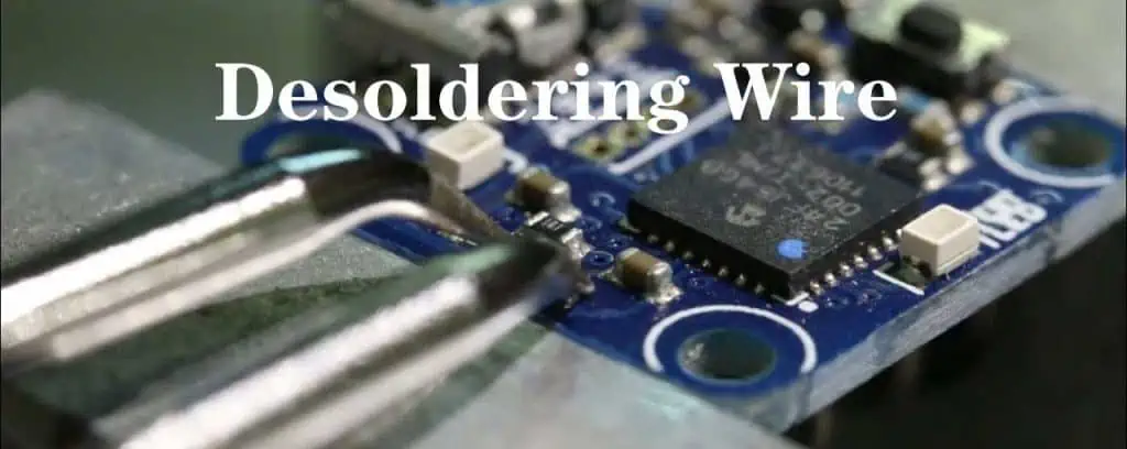
Desoldering Wick

How Does Desoldering Wick Work?
Desoldering wick is also termed a soldering braid or solder wick. It refers to a braided flat copper cable with a flux coating. It absorbs molten solder as the heated soldering iron is put on it. Thus making you able to eradicate the slider efficiently.
When Should We Use A Desoldering Wick?
Desoldering pumps or soldering suckers act as vacuum cleaners, while desoldering wicks act as mops. However, the ability to desolder the wick of solder absorption makes it crucial in applications and devices which do not accept solder splatter.
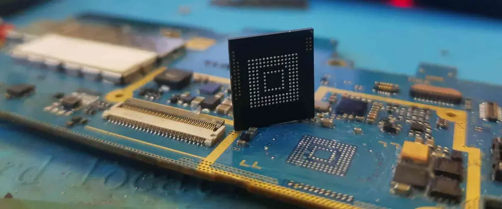
Furthermore, it naturally encourages desoldering wick better at removing off slider from SMT pads along with removing solder gaps on fine pitch BGA and SMT pads found on SMD integrated components PCBs. Though SMD components use special desoldering tweezers or rework stations of hot air to desolder, the desoldering wick also comes in handy.
Whereas a desoldering pump cannot be considered useful for any type of SMD component rework. It happens because of the too-flat conductive pads of PCB, which cannot absorb the solder efficiently. It’s more like drinking soup from a plate with a straw.
Nonetheless, desoldering pumps serve better in desoldering PTH joints. Though a desoldering wick may also do this, capillary action does not have enough efficiency in absorbing a larger quantity of molten solder from an in-depth cavity of a plated through-hole joint. The additional copper braid thermal mass and bigger PTH joint enhance the dwell time. This, however, is risky for both copper trace and electrical components on the Printed Circuit Board.
Selecting A Right Desoldering Wick
Desoldering wicks generally come in 5ft and 10 ft spools, which are also known as bobbins. Bigger spoons come in between the range of 500 ft to 25 ft, but such a large quantity doesn’t suit hobbyists much. Length gives convenience, but choosing a wick with the right width is a very crucial factor to consider.

· Braid Width
Desoldering wicks come in a variety of width options ranging from 0.8 mm to 5 mm. However, according to the thumb rule, the width of the braid must either be exactly equal to the size of the pad or a little larger. Small-size braids will not have the ability to remove the solder from the whole pad, while oversized wicks will impact the nearby pads that you don’t want to desolder.
Moreover, braids with smaller widths also tend the users of the wick to move and take them around during desoldering. This, however, enhances the chances of delaminating the pads from the circuit board. Moreover, an excessively wider desoldering wick also enhances the thermal mass of the components and increases the dwell time on electrical components. Once again, this enhances the chances of Printed Circuit Board pads and electrical components damage.
· Soldering Tip Size
The same reasoning also becomes valid for the tip of the soldering iron. It must match the width of the braid ideally. If the soldering iron has too small a tip, it heats the iron slowly, which enhances the dwell time with the chances of electrical components damaging. Whereas on the contrary, oversized tips of the soldering iron can affect nearby electrical components.
Hoof tips, knives, and chisels fit best for this type of job. Moreover, make sure to avoid utilizing the conical tips of the soldering iron as they have small patch contacts which guide to poor and bad thermal connection.
· Flux Composition
Last but not least, the composition of flux also plays a vital role in the whole desoldering wick. If the workflow demands no-clean solder usage just because you don’t want to clean, then you must utilize a type of desoldering wick with no-clean flux infusion. Whereas, if you wish to clean the Printed Circuit Board Assembly post-type rework, then use rosin flux as they have the fastest wicking action.
Moreover, desoldering wick also comes in the form of no additional flux specifically designed for certain rework processes. Thus, this enables you to utilize your flux which hobbyists usually use to prevent the chances of contamination.
Instructions to Use A Desoldering Wick
Desoldering wick offers a simple process of using it. Here are some steps that help you understand how to use desoldering wicks efficiently.
· Preparing Your Tools
Gather all the necessary equipment and tools like desoldering wick, solder flux, and soldering iron.
· Heating The Soldering Iron
Plug in the soldering iron. Set the temperature and leave it to heat up. The standard temperature relies on the solder type used in the process; therefore, refer to the recommendations of the manufacturer of the solder.
· Positioning The Desoldering Wick
Put a desoldering wick in the place of a solder joint that needs to be removed. However, make sure that a wick entirely wraps the solder.
· Applying Heat
Place the soldering iron head or tip over the desoldering wick right where it makes a connection with a solder joint. Now apply a very gentle force to ensure firm contact.
· Melting The Solder
Heat the joint using a soldering iron which allows the solder to be liquidy and flow over the desoldering wick.t The cooler strands of the wick will later absorb the solder.
· Moving the Wick
Once the solder fully melts down, carefully shift a desoldering wick through the joint while following the molten solder flow. This, however, enables the desoldering wick to absorb solder as much as it can.
· Removing The Wick
Once the desoldering wick absorbs the solder, take off the desoldering wick from a joint. Try to remove the wick carefully as solder, and the wick can still be very hot.
· Inspecting The Joint
Once you remove the wick from a joint, inspect the solder joint to make sure that the molten solder has been appropriately removed. However, if necessary, again, repeat the whole process by desoldering the wick’s new section.
· Cleaning The Tip
Clean the soldering iron tip with the help of a brass cable cleaner or damp sponge to keep its efficiency. This process, however, helps in removing any type of solder flux or residual solder.
Inspecting The Desoldering Wick
Fully examine the wick for signs of clogging or saturation. If the wick loses its ability to absorb or becomes saturated with molten solder, then replace the wick with a new one.
However, always be cautious while working with a soldering iron as it might be very hot to prevent damage or burns to components. Handle all safety measures and use tools with all care.
Desoldering Pump
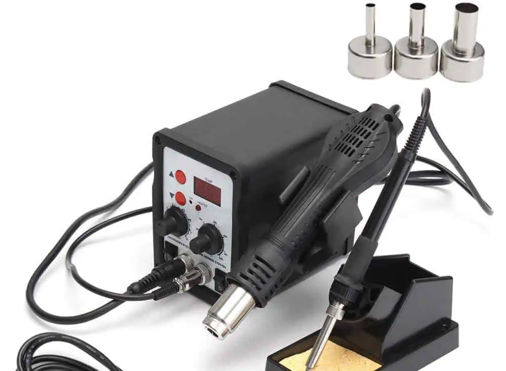
How does It work?
Desoldering pumps are also termed solder extractors or solder suckers which use a spring-loaded function to make suction. On triggering the pump, it quickly sucks away the solder from a joint which makes the removal easier.
How To Use A Desoldering Pump?
Desoldering pump refers to a type of portable machine that offers outstanding services like removing molten solder from the surface of a PCB. It, however, helps in removing the solder after heating it. Here are some steps that help you understand the procedure for using a desoldering pump.
Instructions To Use A Desoldering Pump
- First, apply heat to the molten solder using the soldering iron. However, in some scenarios, the desoldering pump can also come with the soldering iron.
- Second, press the plunger down and apply adequate pressure over it. However, in the case of desoldering pumps that have bulbs, you may squash them.
- Third, after liquifying the solder, place the pump head over the removing molten solder.
- Then comes the discharge or release of the bulb or plunger. Some specific desoldering pumps come with a special design that contains a button for release.
- After that, remove the required free electrical component.
- Repeat the process to fully remove any extra solder from the board.
First, press and then release the bulb or plunger constantly to remove the molten solder within a desoldering pump. The bigger clumps of molten solder have a tendency to remain in the form of liquid for a greater period of time which makes it easy to discard. However, whenever you try to remove extra solder, make sure to add additional solder on the joints.
Here are some specific benefits and drawbacks that both desoldering wick and desoldering pump offers.
Advantages Of Desoldering Wick
· Precision
Desoldering wick provides better accuracy in terms of removing tiny solder balls or dealing with sensitive electrical components. The flexible and thin aspect of a wick enables you to approach specific areas on the board with greater precision.
· Ease Of Use
Desoldering wick allows easy access and easy usage, which makes it easy for beginners to use it. Just simply put the wick over the solder joint, then apply heat on it using a soldering iron tip. Leave it for a few seconds to let the wick suck in the molten solder.
· Cost-Effective
Desoldering wick serves as more affordable and cost-effective than desoldering pumps as it allows you to use them multiple times, which makes it a reasonable and budget-friendly choice for regular desoldering activities.
· Accessibility
Desoldering wick comes in a variety of types and sizes which makes the availability and purchase easy.
Disadvantages Of Desoldering Wick
· Flux Consideration
Desoldering wicks already come with a coating of flux on it which allows the absorption of solder. But the flux may lose its efficiency or dry out with time; therefore, you may need to add extra flux for better results.
· Slower Desoldering
Desoldering wick consumes greater time in removing various soldiers than desoldering pumps, particularly for comprehensive desoldering activities.
Advantages Of Desoldering Pump
· Efficiency
Desoldering pumps serve to remove larger amounts of molten solder quickly. They generally come in handy when working with bigger electrical components or solder joints that need a robust suction force.
· Cleanliness
Desoldering pumps collect the removed molten soldering in a different chamber which helps in keeping the work space cleaner. However, this lessens the risk of molten solder splatter. Also, making the disposal of removed solder waste easy.
· Reduced Heat Exposure
Desoldering pumps enable the soldering joints to expose to a lesser amount of heat than desoldering wicks. However, this proves helpful in dealing with delicate PCBs or heat-sensitive electrical components.
Disadvantages Of Desoldering Pump
· Limited Precision
Desoldering pumps do not provide the same amount of precision level as desoldering wicks do whenever it deals with sensitive components or removes less amount of molten solder.
· Maintenance
Desoldering pumps need occasional maintenance and cleaning to enable optimal performance. Debris or clogs can dramatically impact the action of suction of a pump.
· Cost
Desoldering pumps cost a little higher as compared to desoldering wicks, which may prove helpful for people with tight budgets.
Conclusion
Both Desoldering Pumps and Desoldering Wicks come with their own benefits. Desoldering provides cost-effectiveness, ease of usage, and precision, whereas a desoldering pump offers cleanliness and efficiency and lessens exposure to heat.
Make sure to consider some important factors like desoldering nature requirements, components involved in the process, and some other factors which help in choosing the best tool. However, for a safe passage, take both the dealing pump and the desoldering wick in the toolkit. As this not only enhances the versatility but also makes you handle a variety of desoldering tasks with ease.