What Is Difference Between PCB Slip Ring and Split Ring?

Slip rings and split rings are two important devices used in electrical and mechanical systems for transmitting power and signals across rotating interfaces. Both allow transmission between stationary and rotating components, but have some key differences in their design and applications.

In this article, we will provide a detailed comparison between PCB slip rings and split rings, including:

  • Definitions and working principles
  • Construction and design
  • Materials and manufacturing
  • Performance characteristics
  • Advantages and disadvantages
  • Typical applications
  • Main differences summarized

Understanding the differences between slip rings and split rings enables selecting the right device for different use cases requiring rotary transmission.

Defining Slip Rings and Split Rings

What is a Slip Ring?

A slip ring is an electromechanical device that allows transmission of power and electrical signals from a stationary source to a rotating structure. It consists of a stationary part called the stator, and a rotating part called the rotor.

The stator contains conductive rings that are electrically insulated from each other. The rotor contains metal brushes that make sliding contact with the rings on the stator. As the rotor turns, the brushes maintain continuous electrical connection by sliding over the rings, allowing transmission of power/signals across the rotating interface.

Diagram showing construction of a slip ring.

Common configurations of slip rings include:

  • Pancake slip ring – Rings are arranged in a flat stack.
  • Cylindrical slip ring – Rings are arranged concentrically on a cylinder.
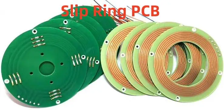
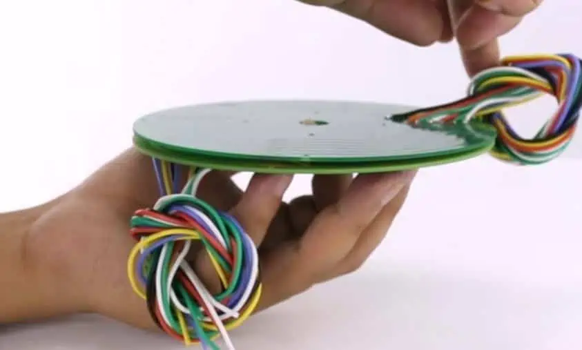
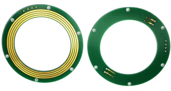
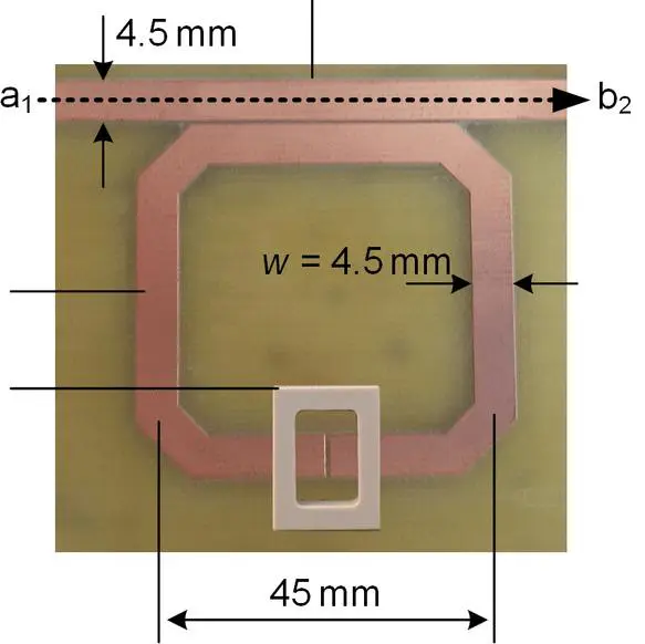
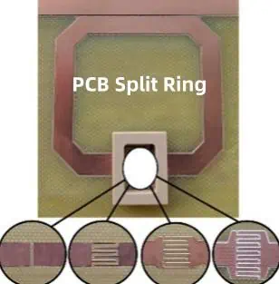
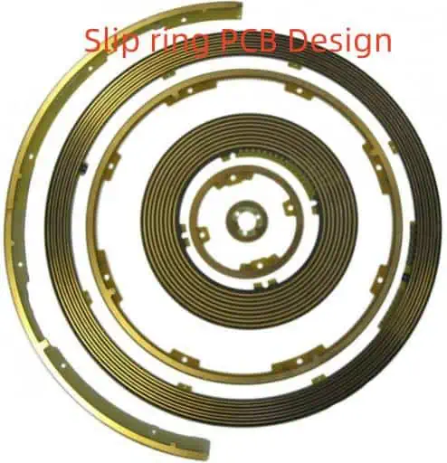
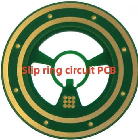
  • PCB slip ring – Rings are etched on a printed circuit board.

Slip rings are bidirectional and can transmit power/signals in both directions across the rotating interface. They allow transmission of low to high power, as well as a wide range of analog and digital signals.

What is a Split Ring?

A split ring, also called a brush block commutator, is a modified slip ring designed to transmit only low power signals or currents in one direction across a rotating interface.

It consists of a rotor assembly containing conductive segments or poles isolated from each other by small gaps. Stationary brushes contact these rotating poles to transmit signals.

As the rotor turns, the brushes make sliding contact with each pole in sequence, allowing transmission in only one direction – from the rotating poles to the fixed brushes. The small gaps between the poles prevent reverse transmission or short circuiting between segments.

Diagram showing construction of a split ring.

Split rings are unidirectional and can only transmit signals in one direction – from rotor to stator. They are suitable for low power signals, and not for high power transfer.

Construction and Design

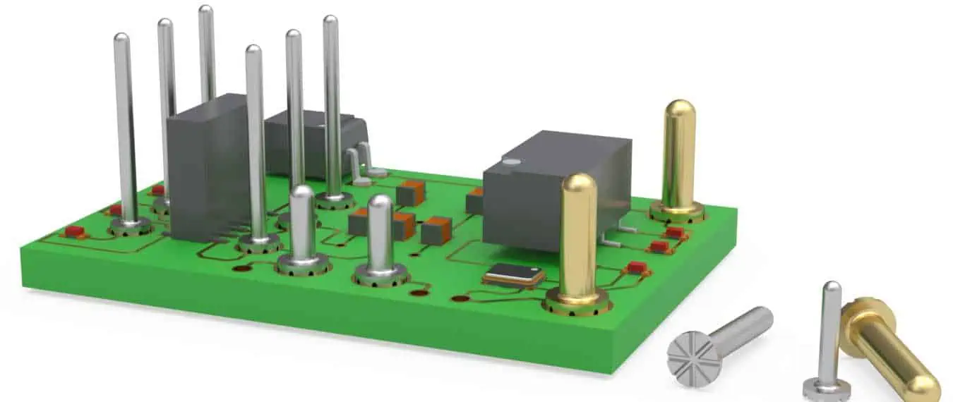
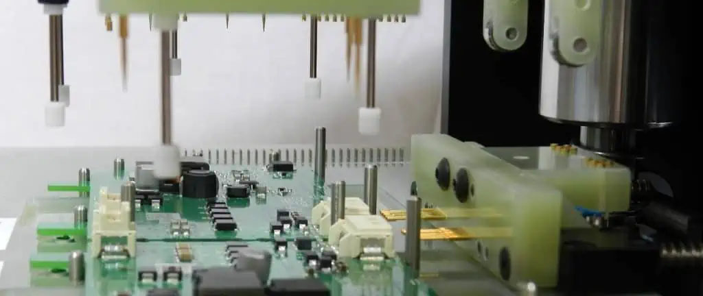
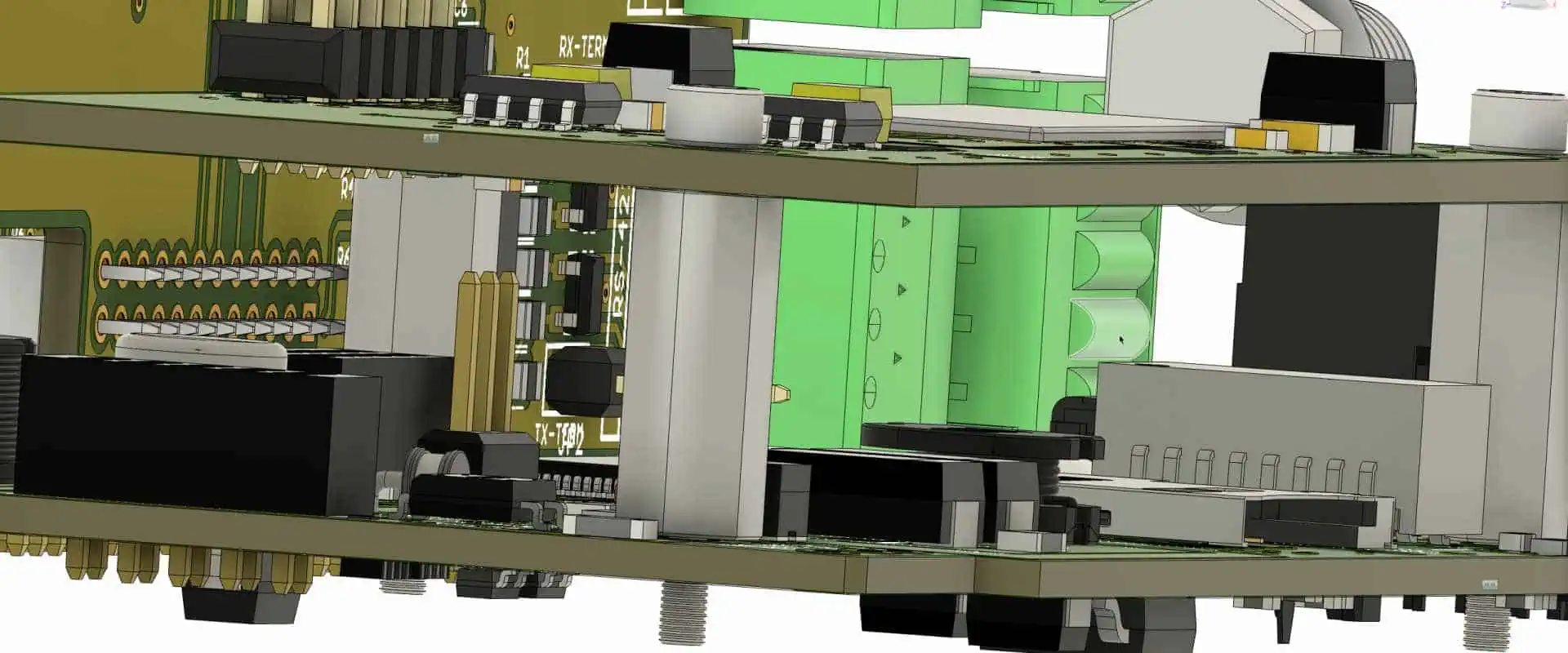
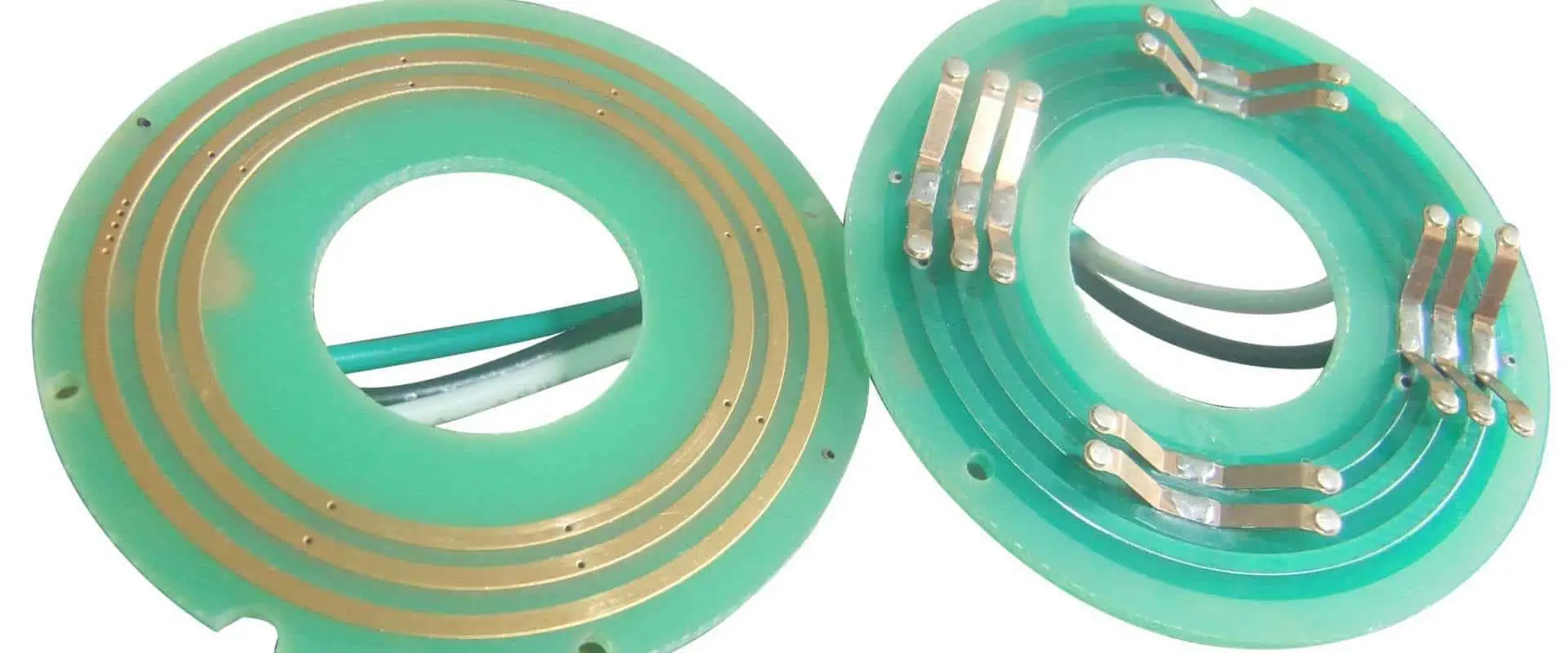
PCB Slip Ring Construction

PCB slip rings are constructed from rings etched on a printed circuit board, which allows compact construction and precise control of ring placement.

Key components of a PCB slip ring include:

  • Printed circuit board (FR4) that forms the stator, with conductive copper rings etched on one side.
  • Rotor containing metal brushes (copper, bronze, precious metals)
  • Insulating cover/housing enclosing the PCB and rotor assembly
  • Bearings allowing smooth rotation of rotor

The PCB is designed with the required number of concentric copper rings etched at precise intervals needed for circuit contacts. The rotor fits over the PCB and the brushes make sliding contact with the copper rings.

Cross section of a PCB slip ring showing copper rings and rotor brushes.

Advantages of PCB slip rings include compact size, easy manufacturing, precise control of tracks, and fast assembly.

Split Ring Construction

Split ring construction consists of a rotor containing segmented conductive poles separated by small air gaps. Common materials used include copper, brass or steel.

The rotor mounts on a bearing and is enclosed in a housing. Brushes are fixed to the stator housing and make sliding contact with the rotor poles.

As the rotor turns, the brushes consecutively connect with each rotor pole, allowing transmission from rotor to stator. The gaps between the poles prevent reverse transmission through the brushes.

Diagram of a split ring showing segmented rotor poles and fixed brushes.

Split rings provide unidirectional transmission and are suitable for intermittent signal contacts. Their simple construction allows low cost manufacturing.

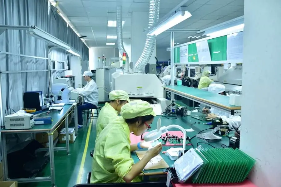
Materials and Manufacturing

PCB Slip Ring Materials

PCB slip rings are manufactured from the following materials:

  • Printed Circuit Board (FR4) – Forms the stator containing the copper ring tracks. FR4 provides electrical insulation between rings.
  • Copper – Used to etch the conductive rings on the PCB. Provides excellent conductivity.
  • Precious metal brushes (gold, silver, palladium) – Used for contacting the copper rings due to high durability and low contact resistance.
  • Plastics like PTFE, PEEK – Used for casing and flange components. Provide mechanical stability.
  • Bearings – Allow smooth rotation and consist of steel balls/rollers with a plastic retainer.

The PCB fabrication process allows high precision patterning of ring tracks in different configurations. The brushes are designed for stable low-friction contact and minimal wear. High quality materials ensure reliability with prolonged use.

Split Ring Materials

Split rings use the following common materials:

  • Copper, brass or steel for the rotor segments. Copper provides the best conductivity.
  • Precious metal brushes (silver, gold) for low contact resistance and reduced oxidation.
  • Plastic housings like nylon, PTFE to enclose the rotor and provide insulation.
  • Bearings using steel balls/rollers to enable smooth rotor rotation.

Split rings use basic materials that provide stable performance at low cost. The materials offer reasonable durability with low friction contacts between the brushes and rotor segments.

Performance Characteristics

PCB Slip Ring Performance

PCB slip rings provide the following performance characteristics:

  • Number of circuits – Can support 10 to 100+ ring contacts for multiple circuits.
  • Current rating – Handle currents from a few mA to over 100 A. Gold brushes allow up to 500 A on each ring.
  • Voltage rating – Rated up to 1000V AC/DC for standard designs.
  • Speed – Standard rings allow rotational speeds up to 1000 rpm. High speed rings support above 5000 rpm.
  • Temperature range – Operate from -40ยฐC to +80ยฐC. Special designs work upto 250ยฐC.
  • Noise – Low noise of 10-50 mฮฉ allows transmission of sensitive signals.
  • Contact resistance – Brush contact resistance of 1-10 mฮฉ allows high power transfer.
  • Lifetime – Brush lifetime over 100 million rotations with precious metal contacts.
  • Isolation – Up to 1000V isolation between adjacent rings.

PCB manufacturing provides precise ring dimensions and spacing for reliable transmission of multiple power/data circuits.

Split Ring Performance

Split rings have the following typical performance ratings:

  • Current – Maximum current around 15-20A. Only suitable for low power signal transmission.
  • Voltage – Maximum voltage rating up to 60V DC.
  • Speed – Standard split rings rated for speeds up to 3000 rpm.
  • Poles – Typical number of poles is 6 to 20. More poles allow more brush contacts.
  • Temperature – Operating temperature range of -20ยฐC to +80ยฐC.
  • Noise – Prone to electrical noise due to brush arcing.
  • Contact resistance – Brush contact resistance around 50-100 mฮฉ. Higher than slip rings.
  • Wear – Brush wear out faster than slip rings due to arcing and higher contact resistance.
  • Lifetime – Brush lifetime around 25 million rotations. Less than slip rings.

Split rings are designed for unidirectional transmission of intermittent, low power signals. They offer lower performance than slip rings but at a lower cost.

Advantages and Disadvantages

PCB Slip Ring Advantages

PCB slip rings provide the following benefits:

  • Compact size due to PCB manufacturing
  • Precise control and spacing of ring circuits
  • Low and stable brush contact resistance
  • Low electrical noise for reliable signal transmission
  • High current and voltage capacity
  • High rotational speeds capability
  • Long service life with minimal wear
  • Bi-directional transmission through rings
  • Easy integration and installation
  • Suitable for data and power transfer

PCB technology enables fabrication of small, high performance slip rings with multiple circuit capacity.

PCB Slip Ring Disadvantages

Some disadvantages of PCB slip rings include:

  • More complex manufacturing process
  • Higher cost than basic slip rings
  • Larger minimum diameter required for ring spacing
  • Not easy to repair or replace brushes
  • Precious metal brushes can be expensive
  • Requires smooth rotor shaft and precision assembly

While PCB slip rings provide superior performance, they also have higher costs and complexity than basic slip ring types.

Split Ring Advantages

Split rings offer the following benefits:

  • Simple and low cost construction
  • Compact, lightweight design
  • High speed operation easily achievable
  • Low friction provides smooth running
  • Only basic tools needed for manufacturing
  • Easy to repair and replace brushes
  • No need for special materials or complex production

The simple design of split rings allows them to be manufactured cheaply and used easily in applications requiring only low power transmission.

Split Ring Disadvantages

Some limitations of split rings include:

  • Only allow unidirectional transmission
  • Prone to electrical noise and interference
  • Low power and voltage capacity
  • Limited number of brush contacts
  • Short service life due to brush wear
  • Cannot transmit high speed data or multiple signals
  • Contact resistance is higher than slip rings
  • Not suitable for continuous power transfer

Split rings are not capable of the bi-directional, high power and data transmission possible with slip rings. Their design and materials impose limits on performance.

Typical Applications

PCB Slip Ring Applications

Some common applications of PCB slip rings include:

  • Industrial machinery – To transmit control and telemetry data between stationary controls and rotating machinery.
  • Medical equipment – MRI machines, CT scanners, etc. use slip rings to transfer signals/power.
  • Avionics – Used in radar systems, control surfaces, weapon turrets that must rotate continuously.
  • Robots – For transferring signals between robot base and rotating joints or platform.
  • Amusement rides – Used on rotating food trays, lighting rings and ride platforms.
  • Wind turbines – Allow power transfer from rotating turbine hub to stationary conductors.
  • CCTV cameras – Enable continuous video feed transmission from pan-tilt security cameras.

PCB slip rings are used anywhere continuous, bi-directional transmission under rotation is needed. Their compact size and high performance allow integration into complex systems.

Split Ring Applications

Typical applications of split rings include:

  • Low voltage electric motors – For periodic power transmission to rotor coils.
  • Automotive systems – Used in sliding door connectors, seat and mirror controls.
  • Rotating displays – For transmitting display data from stationary controllers to rotating signboards.
  • Assembly machinery – Allow power and control signals to rotating tool heads and positioners.
  • Material handling – Used on continuously rotating conveyors and sorters for sensor signals.

Split rings are suitable for cost-sensitive, unidirectional transmission applications that only require low power or occasional contacts.

Main Differences Between Slip Rings and Split Rings

ParameterPCB Slip RingsSplit Rings
ConstructionCopper rings etched on PCB. Precious metal brushes.Segmented rotor poles separated by gaps. Metal graphite brushes.
TransmissionBi-directional – Signals can pass in either direction.Unidirectional – Transmission only from rotor to stator.
Power ratingUp to 100s of Amps, 1000s of Volts.Less than 20A, under 60V.
SpeedUp to 5000 rpm for standard rings. High speed rings even higher.Around 3000 rpm max speed.
NoiseVery low electrical noise. Suited for sensitive data.Prone to electrical noise due to arcing.
Contacts10 to 100+ separate isolated contacts.Typically 6 to 20 contacts.
Resistance1-10 mฮฉ brush contact resistance.50-100 mฮฉ typical contact resistance.
Service life100 million rotations or more.Around 25 million rotations max.
CostHigher cost due to advanced materials and production.Low cost because of simple construction.
ApplicationsIndustrial, medical, military, robotics. For high speed data, video, power transmission.Low power motors, basic machinery, intermittent signals.

Conclusion

PCB slip rings and split rings both allow transmission across rotating interfaces, but have major differences in their design, capabilities and applications.

Key Points:

  • PCB slip rings use precise etched copper rings to enable bi-directional, low noise transmission of multiple power and data circuits simultaneously.
  • Split rings consist of an insulated rotor with segmented contacts, allowing only unidirectional, intermittent signal transmission.
  • Slip rings handle high speeds, power, voltages and lifetimes. Split rings are limited to low power signals and shorter lifetimes.
  • PCB manufacturing provides slip rings with small sizes but higher cost. Split rings have simple construction but lower performance.
  • Slip rings are used where high speed rotation and reliable transmission are needed. Split rings find use in cost-sensitive applications requiring only simple unidirectional contacts.

In summary, PCB slip rings are the preferred choice wherever continuous, reliable transmission of power and high-speed data in both directions is required – such as in precision industrial machinery, robotics, medical systems and military applications. Split rings are suitable for basic low cost systems involving only simple unidirectional signal contacts, like low voltage motors, basic automated systems and rotating displays.

How To Solder And Desolder Header Pins On PCB ?

Header pins are versatile through-hole components used to make removable connections between printed circuit boards (PCBs) and wires or cables. They allow boards to be interconnected or provide test points for diagnostics. Soldering headers securely is essential for reliability. Desoldering damaged headers then allows replacement. This article provides best practices on hand soldering and desoldering header pins to achieve robust, reproducible connections.

Header Pin Overview

Headers come in single, double, and multi-row configurations up to 50 pins or more. Common header types:

  • Male pin headers
  • Female socket headers
  • Straight and right-angle versions
  • Single and double row
  • Through-hole and surface mount styles
  • Common pins sizes from 0.6mm to 1.27mm diameter

Headers are manufactured from tin-plated copper alloy leads inserted into a supporting plastic body. The plastic provides insulation between pins.

Soldering Header Pins

YouTube video

Follow these steps to hand solder headers to a PCB:

1. Prepare the Header Pins

  • Check the header fits into the PCB holes without forcing. Reject if pins are bent or defective.
  • Pre-tinning the header pins can improve solder flow but is not required if using rosin-core solder.
  • For high temperature solders (over 275ยฐC), pre-tinning may be needed to prevent damaging the plastic.
  • Flux paste can be applied to pins and pads to aid solder flow.

2. Prepare the Board

  • Clean any oils, contamination, or oxides from the header pads using isopropyl alcohol.
  • Inspect pads under magnification to ensure there are no solder mask issues or open circuits.
  • Apply solder paste to pads if not using rosin-core wire solder. Match paste alloy to wire alloy.
  • Place the PCB on an ESD-safe work surface and secure with clamps or vise.

3. Insert the Header

  • Carefully insert the header into the mating PCB holes without bending pins.
  • Position the plastic snugly against the board surface.
  • Ensure the header sits straight and flat against the board.
  • Visual alignment marks aid placement for polarized headers.

4. Tack Solder Each Pin

  • Use a small, clean soldering tip suited to the pin pitch. Conical tips work well.
  • Set iron temperature for the solder alloy used. 300-375ยฐC is typical.
  • Lightly tack one pin on each end first to temporarily hold the header in place.
  • Solder remaining pins on one side with 1-2s heat per joint. Avoid bridging between pins.
  • Flux reduces bridging risks. Clean tip frequently.
  • Inspect each joint under magnification after soldering. Reflow if needed.

5. Finish Soldering

  • Solder remaining pins on the opposite side of the header using the same technique.
  • Recheck all pins for full fillets, no bridges, and straight alignment.
  • If pins shift during soldering, reheat and realign.
  • Clean flux residues if needed with isopropyl alcohol.

6. Post Solder Inspection

  • Use an inspection microscope to carefully check each joint around the entire header.
  • Reflow and resolder any joints with insufficient wetting, voids, or other defects.
  • Confirm there are no solder bridges between adjacent pins.
  • Headers should remain fully aligned without tilting or raising from the board.

Following this systematic soldering process will produce reliable, trouble-free header connections.

Desoldering Header Pins

Desoldering may be needed to replace a damaged header or change the configuration. Use the following process to safely desolder headers:

1. Clean Header Joints

  • Remove any conformal coating from the header area using alcohol or coating stripper.
  • Thoroughly clean solder joints of contaminants with degreaser. Flux remover can also be used.

2. Pre-Heat the Header

  • Set the soldering iron tip temperature to ~350ยฐC.
  • Apply heat simultaneously to the header plastic and a few pin joints.
  • Gradually increase temperature to avoid damaging plastic.
  • Heat both sides of header to evenly pre-heat all joints.

3. Desolder Each Joint

  • Using a narrow conical desoldering tip, apply heat to melt each solder joint.
  • Simultaneously use a desoldering pump or wick to remove the liquefied solder.
  • Take care not to apply excess force that may lift pads or damage plated-through holes.
  • Desolder one side of header completely before moving to the other side.

4. Remove the Header

  • Once both sides are fully desoldered, the header will detach easily from the board.
  • Elevate pins on each end alternately to gradually walk the header free.
  • If a short stub remains in a plated hole, use a desoldering tip to remove it.
  • Do not force or pound on the header which can damage the board.

5. Clean and Inspect

  • With header removed, thoroughly clean solder residue from pads using wick, pump, or cleaning solution.
  • Inspect each pad under magnification to ensure there are no lifted or damaged pads or holes.
  • Alcohol cleaning and mild abrasion can remove stubborn residues.

The board is now ready for a new replacement header to be soldered in place.

Hand Soldering Technique

Follow these techniques to hand solder headers successfully:

  • Use a temperature controlled iron or station for consistency.
  • Match tip size to pin pitch to minimize bridging.
  • Tinned copper tips transfer heat efficiently over untinned alloy tips.
  • Apply the minimum heat needed to reflow the joint to avoid damaging plastic or PCB.
  • Keep the soldering iron clean and tinned. Wipe frequently on a damp sponge.
  • Quality no-clean flux cores promote excellent solder flow and wetting.
  • Inspect every joint thoroughly under magnification after soldering.
  • Adjust process based on results – more heat, flux, or time if needed.

Good hand soldering skills take practice but are essential for quality PCB production.

Troubleshooting Guide

Problem: Solder bridges between pins

Solution: Use smaller tip, lower heat, less solder, and flux to prevent bridges. Inspect closely and clean any bridges with braid.

Problem: Cold solder joints

Solution: Increase heat or time to properly reflow joint. Flux and pre-tinning also helps. Rework unsoldered joints.

Problem: Pins lifting pads or shifting

Solution: Avoid putting lateral stress on pins during soldering. Remove and realign crooked pins.

Problem: Solder not wetting to pin

Solution: The pad or pin may be oxidized. Clean and reapply flux before resoldering.

Problem: Cracked or damaged plastic

Solution: Reduce soldering temperature and pre-heat plastic before soldering to avoid thermal shock.

Problem: Desoldering damage

Solution: Carefully pre-heat before desoldering, and never force or pound on the header which can damage the board.

Process Control

Consistent Quality

  • Use written procedures for hand soldering
  • Train operators on process requirements
  • Audit workmanship frequently under microscope
  • Document all process parameters

Traceability

  • Record solder wire and flux batch used
  • Track oven profiles and iron tip temperatures
  • Link parameters to individual boards and lots

Data-Driven Control

  • Log any defects discovered
  • Analyze defects for root cause
  • Optimize parameters to reduce defects

Controlling the soldering process improves yields, lowers rework, and ensures consistent header connections.

Frequently Asked Questions

What is the most common header pin diameter?

The most widely used diameter is 0.6 mm which offers ease of soldering while supporting a variety of wire gauges. 1.27 mm is also popular for high current applications.

Is it always necessary to pre-tin header pins?

Pre-tinning can help solder flow but is not essential if using a rosin-core solder and proper technique. It may be needed for solder alloys requiring higher temperatures.

What causes header pins to become crooked during soldering?

Applying uneven lateral stress, improper hole clearances, misaligned pins, or poor solder joints can all cause pins to shift out of alignment during soldering.

Can solder flux damage a PCB?

Yes, acidic flux can corrode copper pads and traces if not cleaned after soldering. Use no-clean flux designed for electronics. Clean any pastes or residue after soldering.

What is the benefit of breadboarding a header first?

Breadboarding allows checking the header fits and functions properly before permanent soldering. Doing so avoids potential rework if issues are found.

Conclusion

Soldering header pins onto PCBs requires following good hand soldering practices. Using the proper techniques and controls for heating, wetting, fluxing, and pin alignment minimizes defects like bridges and tombstoning. Similarly, careful desoldering prevents damage to the board. Consistent quality soldering produces durable, reliable header connections able to withstand vibration, shock, and repeated mating cycles over the product lifetime.

PCB Solutions: Design, Manufacturing, Assembly, Testing

Printed circuit boards (PCBs) are core components in nearly all modern electronic devices. Developing a successful PCB solution requires expertise across the entire process from initial design through volume production. This article provides a comprehensive overview of end-to-end PCB solutions encompassing design, layout, fabrication, assembly, test, and finally deployment into products. It covers key considerations and options at each stage to deliver a robust, high-quality PCB ready for integration.

PCB Design

The design phase transforms electrical requirements into physical board layout and documentation.

Schematic Capture

A schematic editor is used to diagram the circuit connections between components. This schematic drives layout and manufacture.

  • Capture all connections and nets
  • Follow schematic conventions for readability
  • Manage component library

Simulation and Verification

Simulate circuit performance to verify functionality before layout:

  • Analog/digital circuit simulation
  • RF/signal integrity analysis
  • Thermal modeling
  • Mechanical stress simulation

Layout

Transfer the schematic into board geometry within a PCB layout tool:

  • Place components and route connections
  • Ensure design manufacturability
  • Manage board layers and stackup
  • Produce manufacturing Gerber files

Design for Manufacturing (DFM)

Apply DFM practices to ensure the design can be successfully manufactured:

  • Follow fabrication capabilities
  • Allow tolerances for alignment
  • Enable testability
  • Facilitate assembly

Documentation

Generate drawings, models, specs, and notes for fabrication and assembly:

  • Component list (bill of materials)
  • Assembly drawings
  • 2D/3D models
  • Fabrication callouts
  • Impedance requirements
  • Board stackup

Thorough documentation prevents errors and minimizes ambiguity for PCB production.

PCB Fabrication

Fabricating the designed PCB involves complex processes.

Selecting a Fabricator

Choose a fabrication partner able to meet:

  • Technology requirements (layer count, density, line width)
  • Quality and reliability standards
  • Volume capabilities
  • Cost targets
  • Lead time needs

Fabrication Process

Typical PCB manufacturing steps:

  • Laminating – Building up board layer structure
  • Drilling – Creating holes for vias and components
  • Plating – Electroplating copper on hole walls
  • Etching – Removing copper to form traces
  • Solder mask – Applying protective coating
  • Silkscreen – Printing informational labels
  • Finishing – Edge treatments and surface plating
  • Electrical test – Validating continuity
  • Quality inspection – Verifying specifications are met

Testing and Inspection

Ensure fabricated boards are defect-free through:

  • Automated optical inspection (AOI)
  • X-ray inspection
  • Electrical testing
  • Impedance testing
  • Solderability testing

Documentation

  • Generate fabrication drawings
  • Supply bill of materials
  • Provide assembly instructions
  • Include any special notes or handling requirements

PCB Assembly

through-hole assembly process

Populating fabricated boards with components requires advanced manufacturing.

Selecting an Assembler

Determine an assembly partner meeting:

  • Technology capabilities
  • Quality and reliability needs
  • Volume capacity
  • Cost targets
  • Supply chain resource

Assembly Processes

Common assembly steps include:

  • Solder paste printing – Apply solder paste pads
  • Component placement – Mount parts on paste pads
  • Reflow soldering – Heat boards to form solder joints
  • Through-hole insertion – Add through-hole components
  • Wave soldering – Solder bottom-side pads
  • Conformal coating – Protect boards from environmental exposure
  • Cleaning – Remove flux residues

Automated Assembly

Use automated pick-and-place and soldering for:

  • Higher throughput
  • Improved consistency
  • Lower costs at volume
  • Small component handling

Testing and Inspection

Verify assembly quality and component placement:

  • In-circuit test (ICT)
  • Functional test
  • X-ray inspection
  • Optical inspection

Documentation

Supply assembly partner with:

  • Bill of materials
  • Centroid files for pick-and-place
  • Soldering profiles
  • Test requirements
  • Acceptance criteria

Test and Verification

Confirm boards function properly before deployment.

Design Verification Testing

Validate the design meets all electrical performance requirements:

  • Functionality testing
  • Parametric limits testing
  • Margins testing
  • Environmental stress testing

Production Testing

Check each production board for defects and consistency:

  • In-circuit test (ICT)
  • Flying probe
  • Boundary scan
  • Functional test

Debug and Diagnostics

Troubleshoot any faults or issues found:

  • Failure analysis
  • X-ray and thermal imaging
  • Signal probing
  • Optical inspection

Testing at multiple stages catches defects early and ensures quality.

Documentation

Maintain records of:

  • Test procedures
  • Test reports
  • Debug logs
  • Failure analysis reports
  • Corrective actions

Deployment

Deploy boards into final products and maintain through lifetime.

Integration and Installation

Prepare boards for system integration:

  • Program firmware/software
  • Configure settings
  • Burn-in to stabilize components
  • Final inspection

Qualification Testing

Validate performance meets system requirements:

  • Long term reliability testing
  • Thermal cycling
  • Vibration and shock exposure
  • Lifetime testing

Maintenance and Support

Provide continuity of supply and repair:

  • Monitor for emerging defects
  • Component obsolescence mitigation
  • Repair capabilities
  • Replacement part stocking

Documentation

  • As-built configuration documentation
  • Maintenance procedures and repair manuals
  • Lifetime warranties
  • Application notes

Conclusion

Delivering complete PCB solutions requires expertise spanning design, fabrication, assembly, test, and lifetime maintenance. Choosing the right partners and processes at each stage results in a ruggedized PCB ready for integration into products. A holistic approach reduces risk and total cost while accelerating time-to-market.

Frequently Asked Questions

What are the main steps in the PCB development process?

The core PCB development steps are:

  1. Design – schematic capture, layout, documentation
  2. Fabrication – producing bare boards
  3. Assembly – soldering components onto boards
  4. Test – validating board function and quality
  5. Deployment – integrating into products and systems

What are key design for manufacturing guidelines?

Some key DFM guidelines are:

  • Allowing adequate tolerances
  • Following manufacturer design rules
  • Incorporating testability features
  • Facilitating assembly and inspection
  • Standardizing components and footprints

What fabrication steps create the PCB trace layers?

The combination of laminating copper foil, drilling holes, electroplating copper, and chemical etching produces the patterned copper traces comprising the PCB layers.

What are some common PCB assembly process defects?

Typical assembly defects include:

  • Missing or incorrect components
  • Solder shorts
  • Insufficient solder
  • Solder balls
  • Damaged pads/traces
  • Board warp/twist

When is automated optical inspection (AOI) used?

AOI machines quickly scan assembled PCBs to identify defects like missing components, poor solder joints, or misalignments. It provides fast in-line inspection.

What is PCB Standards?

Printed circuit boards (PCBs) are at the heart of electronics, providing the foundation for mounting and interconnecting electronic components using conductive copper traces. PCBs come in an endless combination of materials, sizes, layer counts and complexities to suit diverse applications.

To ensure quality, consistency and compatibility across the electronics hardware ecosystem, PCB fabrication and assembly adheres to a set of well-defined industry standards. PCB standards provide specifications and guidelines governing vital aspects of materials, design, manufacturing and testing.

This article provides an overview of key PCB standards bodies, the purpose of PCB standards, design rule principles, fab and assembly process standards, and testing/inspection norms relevant for PCB production.

PCB Standards Bodies

PCB IPC standards

PCB standards are developed and published by professional organizations who aim to promote best practices and unified norms across the industry. The most notable standards bodies include:

  • IPCย – Association Connecting Electronics Industries
  • IEEE – Institute of Electrical and Electronics Engineers
  • IEC – International Electrotechnical Commission
  • JEDEC – JEDEC Solid State Technology Association
  • ANSI – American National Standards Institute
  • DIN – Deutsche Institut fรผr Normung (German Institute for Standardization)
  • JIS – Japanese Industrial Standards Committee

These entities collaborate with PCB manufacturers, electronics companies and government agencies to evolve standards addressing emerging needs. IPC and IEEE standards dominate the PCB industry.

Some standards are globally adopted, while others are more regional. However, common foundational principles run through most significant PCB standards.

Importance of PCB Standards

Well-defined PCB standards provide a variety of benefits:

  • Quality – Standards ensure consistency in materials and processes. This improves manufacturing quality.
  • Compatibility – Common design norms allow PCBs from different vendors to interoperate.
  • Interchangeability – Standard components and features enable interchangeability.
  • Reliability – Adhering to accepted test procedures improves field reliability.
  • Safety – Standards for insulation resistance minimize electrical hazards.
  • Communication – Standards like documentation symbols facilitate communication.
  • Innovation – Standards free up development resources to focus on innovation rather than basics.
  • Cost savings – Economies of scale lower costs when following standards.
  • Regulations – Standards help the industry conform to environmental regulations.
  • Global trade – Universal standards enable global import/export of PCBs and electronics hardware.

In essence, standards aim to maximize quality, reliability and productivity across the industry.

PCB Design Standards

PCB design standards establish norms for:

  • Materials – Specifications for substrate (fiberglass, ceramic etc.) thickness, copper weight, dielectric constants, etc.
  • Layers – Guidelines for number of conductive layers, copper thickness per layer, clearance between layers, etc.
  • Dimensions – Standard PCB sizes like 160mm x 100mm, 233mm x 160mm, or custom max dimensions.
  • Line Width/Spacing – Minimum trace width and spacing between traces based on voltage.
  • Via Styles – Types of plated through hole vias – thru hole, blind, buried, microvia – and their dimensions.
  • Clearances – Minimum electrical clearance between pads, tracks, holes and board edge.
  • Finishes – Recommended surface finishes like HASL, immersion silver, ENIG (Electroless Nickel Immersion Gold), etc.
  • Coatings – Specifications for solder mask, silkscreen and other protective coatings.
  • Markings – Board identifier nomenclature, date codes, revision numbering and other marking guidelines.
  • Documentation – Recommended formats for schematics, assembly drawings, fabrication drawings.

These fundamental standards allow PCBs to support components, connectors and technologies reliably. They promote manufacturability across different vendors.

Design Rules in PCB Standards

PCB design standards outline constraints known as design rules which specify acceptable limits for parameters like tracks, holes, spaces, masks, laminates, etc.

Design rules aim to ensure:

  • PCBs can be reliably manufactured using available fabrication processes
  • Completed PCBs work properly without faults or performance issues
  • Designs meet safety needs of the end product

Some key PCB design rules cover:

  • Minimum hole size for through hole components
  • Minimum annular ring for holes
  • Minimum spacing between copper elements
  • Minimum track width and clearance
  • Mask expansion margins from pads
  • Silkscreen keepout areas around pads

Tool-specific design rules:

  • Trace impedance requirements
  • High speed length matching constraints
  • Plane connection requirements
  • Specific pad shapes needed
  • Allowed via types

Complex rules help maintain signal integrity, high speed performance and reliability. PCB design tools automatically check rules. Waiving certain rules is possible through review and testing.

PCB Fabrication Standards

standard 4 layer stackup

PCB fabrication standards ensure consistency in materials, quality and reliability across PCB manufacturing processes like:

  • Lamination – Number of high pressure presses, temperature profiles, global vs local lamination.
  • Drilling – Hole position accuracy, hole wall quality, drill bit sizes and wear.
  • Via Formation – Copper plating thickness inside plated through holes and vias.
  • Outer Layers – Copper thickness, foil types, dimensional accuracy, registration.
  • Inner Layers – Alignment between layers, lamination adhesion, bond enhancers.
  • Coatings Application – Photoresist, solder mask, legend ink curing and adhesion.
  • Metallic Finishes – Thickness and properties of ENIG, immersion tin, other platings.
  • Electrical Test – Continuity testing, open/short detection, netlist verification.
  • Impedance Control – Methods for controlled impedance tracks.
  • Hole Wall Quality – Standards for desmear, etchback, hole wall roughness.
  • Panelization – Board depaneling, breakaway tab designs.

These manufacturing standards enable producing the designed PCB reliably in high volumes across vendor facilities.

PCB Assembly Standards

SMT QC
SMT QC

PCB assembly standards cover prototyping, low volume and mass production assembly of components on fabricated boards:

  • Soldering – Methods like wave, reflow, manual; solder types; solder bath maintenance.
  • Component Handling – ESD (electrostatic discharge) protection, moisture sensitivity procedures, baking.
  • Inspection – Automated optical inspection (AOI) capabilities and limitations.
  • Test – In-circuit test coverage; fixture design; diagnostics.
  • Coatings Application – Conformal coating material specs, coverage criteria, process control.
  • Rework – Conditions warranting rework; manual repair techniques; reballing/replating guidelines.
  • Cleaning – Removal of post-solder flux; solvents and methods.
  • Marking – Component orientation indicators; serial numbers; ink durability.
  • Packaging – ESD bags, desiccants, box styles, humidity indicators, drop test requirements.

Assembly standards maximize throughput yields and long term product reliability.

PCB Testing Standards

Rigorous testing to accepted standards ensures PCBs function as designed:

Materials Testing

  • Glass transition temperature
  • Coefficient of thermal expansion
  • Thermal conductivity
  • Flammability rating
  • Water absorption
  • Flexural strength
  • Bond strengths
  • Dielectric breakdown voltage
  • Surface insulation resistance

Electrical Testing

  • Continuity testing
  • Insulation resistance
  • High voltage testing
  • Impedance testing
  • Propagation delay
  • Signal integrity

Mechanical Testing

  • Vibration testing
  • Shock/drop testing
  • Bend testing
  • Solderability testing
  • Coating adhesion testing

Environmental Testing

  • Thermal cycling
  • Temperature/humidity cycling
  • Salt spray exposure
  • Life testing
  • HASS (highly accelerated stress screen)

Testing to these standards verifies the board can survive real-world operating conditions while maintaining electrical performance.

Documentation Standards

Clear documentation is vital for PCB fabrication and assembly. Relevant documentation standards cover:

  • Schematics – Symbol conventions; layout; netlist format; part numbering.
  • PCB Layout Drawings – Dimensioning format; fabrication layer notes; drills table.
  • Bill of Materials – Approved manufacturer names; component grouping; descriptions.
  • Assembly Drawings – Reference designators; allowable substitutions; callouts.
  • Gerber Files – File naming; format; layer assignments; attributes.
  • Netlist – Netlist format; connection ordering; component designators.
  • Fabrication Specification – Material requirements; acceptance criteria; IPC class.
  • Assembly Specification – Approved assembly processes; inspection criteria; test requirements.
  • Impedance Calculations – Supported tools and formats for controlled impedance reporting.

Standardizing documentation facilitates handoff between design, fabrication and assembly firms. Machine readable data speeds production.

Conclusion

PCB Quality control
PCB Quality control

PCB standards empower quality, scale and technological innovation across the electronics hardware industry. They balance practical manufacturing capabilities with optimizing performance, reliability and cost efficiency.

Knowledge of the most commonly applied standards helps engineers architect designs tailored for manufacturability and commercial success. As PCB technology progresses to integrate new materials and fabrication techniques, standards will co-evolve to incorporate emerging best practices.

Careful application of PCB standards, combined with strategic customization when justified, results in electronics products delivering robust functionality within budgetary constraints. This maximizes return on investment in PCB technology for enabling cutting edge products.

Frequently Asked Questions

Q1: Who establishes official PCB standards?

A1: Professional organizations like IPC, IEEE, JEDEC and IEC develop de facto standards widely adopted across the global PCB industry and supply chain. Regional groups like ANSI, DIN also publish standards.

Q2: How are PCB standards enforced?

A2: PCB standards are voluntary technical specifications. Market forces incentivize adhering to standards to enable compatibility, quality and reliability. Some performance and safety related standards are mandated by regulations.

Q3: Can I custom design a PCB violating standards?

A3: Specific standards may be judiciously waived after careful analysis confirms the design works correctly. Deviating from key electrical and physical design rules risks functionality flaws or manufacturing failures.

Q4: How frequently are PCB standards updated?

A4: PCB standards are updated every 2 to 5 years on average to incorporate technology advancements and new best practices. Changes aim to balance innovation with minimizng retooling costs.

Q5: Where can I find resources explaining PCB standards?

A5: IPC and IEEE provide technical PCB standards resources on their websites. Many are available for free download. PCB tool vendor documentation also explains implementing relevant standards.

What are PCB standoffs for๏ผš Standard Size, Uses and Placement

Printed circuit boards (PCBs) form the core foundation of electronics products by electrically interconnecting components using copper traces on an insulating substrate. PCBs need to be physically secured and separated from external surfaces for proper functioning. PCB standoffs play a vital mechanical role in providing secure mounting and spacing for circuit boards in electronic enclosures and assemblies.

This article provides a comprehensive overview of PCB standoffs covering their definition, key sizes, common uses, optimal placement considerations and installation best practices.

What are PCB Standoffs?

PCB standoffs, also called board spacers, are simple mechanical parts used to mount printed circuit boards and space them at a fixed distance from other surfaces.

They consist of a male and female end. The male end has threads that screw into a tapped hole in the enclosure or chassis. The female end has threads to accept a screw and secure the PCB. This creates separation between the PCB underside and the mounting surface.

PCB standoffs are always used in combination with compatible screws to affix the board. They are made from rigid, durable materials like nylon, brass, aluminum etc. Insulating plastic standoffs prevent electrical shorts.

Key properties and functions of PCB standoffs include:

  • Provide secure physical mounting for PCBs
  • Separate PCB from enclosure or other boards
  • Create space for components on back of PCB
  • Promote airflow and cooling under PCB
  • Prevent short circuits to chassis
  • Absorb vibration and shock
  • Allow washers, spacers etc. to adjust height
  • Reusable across multiple designs
  • Customizable length to suit needs

PCB standoffs are inexpensive, readily available and easy to install. They enable quick prototyping and revisions by allowing boards to be detached and remounted quickly. Multiple standoffs distribute mechanical load evenly across the PCB.

Standard Sizes of PCB Standoffs

PCB standoffs are manufactured in a range of standard sizes described by the stud diameter and length. Common imperial and metric sizes include:

Imperial Standoffs

Stud DiameterCommon Lengths
#4-401/4″, 3/8″, 1/2″, 3/4″, 1″
#6-321/4″, 3/8″, 1/2″, 3/4″, 1″
#8-321/4″, 3/8″, 1/2″, 5/8″, 3/4″, 1″, 1-1/4″
1/4″-201/4″, 3/8″, 1/2″, 5/8″, 3/4″, 1″

Metric Standoffs

Stud DiameterCommon Lengths
M35mm, 10mm, 12mm, 15mm, 20mm, 25mm, 30mm
M45mm, 12mm, 15mm, 20mm, 25mm, 30mm
M55mm, 10mm, 12mm, 15mm, 20mm, 25mm

Standoff lengths between 1/4″ to 1″ are typical for most applications. Longer standoffs are used when increased spacing is needed. Metric standoffs follow ISO standards for thread dimensions.

Standoffs often have a combination of male and female threads in imperial or metric sizes. Standard thread sizes ensure compatibility with common screws and maximize sourcing flexibility.

Uses of PCB Standoffs

PCB standoffs serve many important functions across a wide range of electronic equipment:

Electronic Enclosures

  • Mounting PCBs securely inside metal or plastic enclosures
  • Providing insulation and preventing electrical shorts
  • Allowing access to underside components
  • Permitting washers for height adjustment

Stacked PCB Assemblies

  • Separating stacked circuit boards
  • Maintaining spacing between boards
  • Allowing inter-board connectors

Carriers and Frames

  • Mounting PCBs in slide-in racks and carriers
  • Securing boards into chassis frames
  • Absorbing vibration and shock

Development Platforms

  • Prototyping circuits with easy installation
  • Revising PCBs by remounting quickly
  • Customizing height as needed

Thermal Solutions

  • Providing airflow gap below board
  • Improving convection cooling
  • Allowing heat sinks and cold plates

High Frequency Circuits

Test Fixtures

  • Securing PCBs to test jigs
  • Allowing probe access for testing

PCB standoffs are ubiquitous in electronic products thanks to their versatility, simplicity and low cost. They enable quick design iterations, shielding, cooling, stacking, production testing and much more.

PCB Standoff Placement Guidelines

Proper placement of standoffs is key to maximizing their mechanical benefits for the PCB. Here are some best practice guidelines for standoff placement on PCBs:

  • Near board edges – Standoffs should be close to board corners and edges for stability.
  • Distributed evenly – Spread standoffs uniformly to avoid stress concentrations.
  • On stronger layers – Attach standoffs to thicker, inner board layers for sturdiness.
  • Away from components – Keep standoffs clear of tall components on the backside.
  • Along expansion slots – Use standoffs adjacent to board slots for structural support.
  • Around connectors – Standoffs help relieve connector strain on the PCB.
  • On both sides – When possible, add standoffs on both sides for maximum holding strength.
  • Following enclosure mounts – Match PCB standoff locations to existing enclosure mounts.
  • Considering thermal impacts – Ensure standoffs don’t block airflow paths to heat generating components.
  • Facilitating test access – Position standoffs to enable easy probe access during testing.
  • Allowing service access – Don’t cover debug ports, jumpers and other accessed features.
  • Checking manufacturer guidelines – Follow PCB manufacturer’s guidelines for mechanical support.

Careful standoff placement safeguards PCB integrity through the product’s lifecycle. Slight adjustments enable tuning board performance and accessibility.

PCB Standoff Installation Process

Installing PCB standoffs involves simple steps but needs care to avoid damaging boards or components:

Step 1: Mark Holes

  • Mark desired standoff locations on PCB topside.
  • Select points following placement guidelines.
  • Account for nearby components and features.

Step 2: Drill Holes

  • Use small pilot drill for initial hole.
  • Open up hole to suit standoff diameter.
  • Drill slowly through PCB to avoid cracking.

Step 3: Countersink Holes (optional)

  • Countersink larger holes on component side.
  • Provides flat surface for screw heads.
  • Reduces risk of damage to components.

Step 4: Secure Standoffs

  • Screw male threaded end of standoff into mounting surface.
  • Tighten adequately but avoid over torqueing.
  • Use thread locker for permanent installs.

Step 5: Install PCB

  • Align PCB holes with protruding standoffs.
  • Add washers or spacers if needed.
  • Attach board using screws into standoff female ends.

The installation process can be done manually or integrated into an automated PCB assembly line. Proper torque control and dimensional tolerances are vital for reliability.

Assembly Considerations

Some additional considerations for PCB standoff assembly include:

  • Flat washers – Use flat washers under screw heads to prevent damage to traces. Nylon washers minimize shorts.
  • Shoulder washers – Shoulder washers provide a hard stop, preventing overtightening.
  • Spacers – Additional spacers or standoffs stacks allow adjusting board spacing.
  • Access windows – Cutouts in PCBs can allow accessing standoff screws for easier assembly.
  • Thread locker – Apply thread locking fluid for permanent or vibration-resistant installation.
  • Torque control – Controlled torque screwdrivers avoid overtightening damage during automated assembly.
  • Board support – Support the area around the standoff when screwing in or out to prevent board warping.
  • Repeated assembly – Use new or fresh hardware when re-installing boards to avoid wear and loosening.

Proper techniques and compatible hardware keeps PCB standoffs serving reliably over years of use and rework.

PCB Standoff Materials

PCB standoffs are constructed using materials that balance mechanical stability, electrical insulation and cost:

  • Nylon – Most common material. Offers good strength and insulation at low cost. Available in natural and black colors.
  • Polycarbonate – Provides very high strength but costs more than nylon. Translucent material.
  • Aluminum – Anodized aluminum has excellent mechanical rigidity. Must be insulated from PCB.
  • Brass – Brass standoffs have high stability though not as strong as steel. Corrosion resistant nickel plating is applied.
  • Stainless steel – Very robust but typically avoided due to electrical conductivity without insulation.
  • PEEK – Advanced high-temperature thermoplastic with excellent mechanical and electrical properties. Cost is high.

Nylon provides the best combination of cost, strength, stiffness and insulation for most applications. Other materials offer enhanced specific properties where needed.

Standoff Design Elements

Besides the core stud and threads, PCB standoffs can incorporate additional design elements:

  • Flanged head – Flanged end prevents the standoff rotating when tightening the nut or screw. Useful for thin panels.
  • Jam nut – Separate jam nut provides locking of standoff height. Reduces risk of loosening over time.
  • Phillips / hex drive – Drive tool interface on stud end speeds installation in high volume production. Allows controlled torque.
  • Locating pin – Protruding pin helps align PCB without shifting. Useful for assemblies with hidden standoffs.
  • Shoulder – Internal shoulder provides solid stop when tightening screw. Prevents damage to board or components.
  • Flat base – Flat base optimizes load distribution on panel surface. Reduces point stresses.
  • Cap nut – Low profile cap nut reduces need for tool access above board. Streamlines enclosed installs.
  • Mounting accessories – Clips, brackets, adapters etc. facilitate mounting standoffs in specific applications.

These design options customize PCB standoffs for specialized mechanical, assembly and service needs.

Conclusion

PCB standoffs play an indispensable role as simple mechanical parts enabling secure mounting of printed circuit boards across nearly all electronics sectors and applications. Their standardized materials, dimensions and threading deliver reliable, reusable board mounting.

Optimizing PCB standoff selection, placement and installation practices helps product designers extract maximum value from these oft overlooked components. An intimate understanding of their uses empowers engineers to architect elegant electronics solutions.

As increasing miniaturization and complexity demands enhanced support for delicate PCBs, the humble PCB standoff will continue serving a critical function in electronics product design for the foreseeable future.

Frequently Asked Questions

Q1: How are PCB standoffs sized and specified?

A1: PCB standoffs are sized by stud diameter and length. Standard diameters are #4, #6, #8 imperial or M3, M4, M5 metric threads. Length ranges from 1/4″ to 1″ typically.

Q2: How many standoffs should be used for a PCB?

A2: Use at least 4 standoffs – 1 near each corner. Larger boards benefit from additional standoffs distributed along the edges. Follow manufacturer guidelines for the number.

Q3: Can I use brass standoffs without insulation?

A3: Uninsulated brass standoffs may short connections on the PCB underside. Use plastic insulated brass standoffs or nylon / polycarbonate standoffs to avoid shorts.

Q4: Is thread locker fluid necessary for PCB standoffs?

A4: Thread locker improves vibration resistance and prevents loosening over time. It is recommended for permanent installs. For removable boards, thread locker may hinder future access.

Q5: What precision is needed for PCB standoff hole locations?

A5: Standoff holes can tolerate +/- 0.5 mm placement error. Tighter tolerances improve alignment but are not essential in most cases. Use spacers to correct minor mismatches.

What is a PCB Symbol?

A printed circuit board (PCB) is a board made of insulating material like fiberglass with copper tracks printed on it to connect electronic components. PCBs provide the electrical connections between components in an electronic device like computers, mobile phones, appliances etc.

PCB design involves creating schematics and layouts to represent the circuit connections. PCB symbols are graphical symbols used to represent various electronic components and connections in PCB schematic diagrams and layouts. They help engineers visualize the circuit and wiring connections during the design process.

This article will provide an in-depth explanation of what PCB symbols are, the common symbols used, how to read them and use them in PCB design software.

What are PCB Symbols?

Schematic Symbols

PCB symbols are abstract graphical representations of electronic components and connections used in schematic diagrams and PCB layouts.

They allow electrical engineers to visualize complex circuitry and wiring in a simple graphical manner. The symbols depict the function and connections of components without showing the actual physical appearance.

Some key points about PCB symbols:

  • PCB symbols represent components like resistors, capacitors, integrated circuits, transistors, connectors, wires and other parts found on a PCB.
  • Symbols utilize shapes like rectangles, circles and triangles to depict different components. Lines between symbols show electrical connectivity.
  • Symbols are not drawn to scale – they are conceptual abstract representations.
  • Each symbol represents a packaged component with two or more pins or leads to connect it to other parts of the circuit.
  • Symbols have unique representations across different PCB design software to avoid confusion between similar looking parts.
  • Symbols display the component name, value and other information to identify the specific part.
  • Standardized symbols from IEC and IEEE allow for consistency and readability across different schematics and layouts.

Overall, PCB symbols provide a simple way for design engineers to conceptualize complex PCB circuits and layouts. The visual language enables efficient schematic capture and layout routing.

Common PCB Symbols

There are hundreds of standard PCB symbols used to represent various electronic components and connections. Here are some of the most common PCB symbols found in schematic diagrams and layouts:

Passive Components

Passive components like resistors, capacitors and inductors have simple but distinct representations:

  • Resistorย – Zigzag line showing resistance to current flow. Value displayed in ohms (ฮฉ).
  • Capacitorย – Parallel lines indicating capacitor’s plates to store charge. Value in farads (F).
  • Inductorย – Coiled wire showing induction of magnetic field. Value in henrys (H).

Active Components

Active components like transistors and integrated circuits (ICs) have more complex symbols:

  • NPN Transistorย – Arrows show current flow from base to collector. Circle represents base.
  • Integrated Circuit (IC)ย – Rectangle with pins on sides. Label shows IC name/number.

Connectors

Various connectors are used to interface the PCB with other circuits or devices:

  • Male Headerย – Represented by pin protrusions. Number of pins indicated.
  • Female Header – Shows socket holes for male header. Pin count matches male version.
  • USB Portย – Standard USB symbol used. Indicates host/device with arrow direction.

Power Sources

Power symbols show connections to power sources:

  • DC Supply – Indicates DC power source. Positive (+Ve) and negative (-Ve) terminals shown.
  • AC Supplyย – Symbolizes AC power input. May show voltage value.
  • Ground – Common ground point for returns.

Miscellaneous

Other common symbols found in PCB schematics and layouts:

  • Fuse – Fuse element shown between connections. Current rating displayed.
  • Transformer – Two inductive coils coupled by magnetic field.
  • LEDย – Arrow indicates light emission. Longer lead is anode.
  • Batteryย – Voltage rating displayed inside cell symbol.

This covers some of the most prevalent PCB symbols, though there are many more niche representations for specific components and interfaces.

Reading PCB Symbols

schematic symbols currently drawn

Being able to accurately read PCB schematics and layouts requires understanding how to interpret the symbols correctly. Here are some tips on reading PCB symbols:

  • Recognize the basic symbol shape – Each component has a distinctive symbol. Learn the common shapes like zigzags, coils, rectangles etc.
  • Identify component type from symbol – The symbol directly represents what the component does. For example, capacitor symbols represent a device that stores charge.
  • Lookup unfamiliar symbols – Some symbols may be unfamiliar. Refer datasheets or symbol reference charts to identify them.
  • Note symbol directions and polarities – Arrowheads indicate current flow direction. Plus/minus signs show polarity.
  • Read component names/values – Name and values labeled on symbol provide further identification.
  • Follow connecting lines between symbols – Traces between symbols show electrical connectivity in the circuit.
  • Match inputs and outputs – Interface points on symbols show connections to other components.
  • Note special notations – Symbols may have additional letters, numbers and notes marked.
  • Adhere to industry standards – Most symbols follow standards from IEEE and IEC for consistency.

With practice, an engineer proficiently navigates and comprehends PCB schematics and layouts by correctly interpreting all the symbols depicted.

PCB Design Software Symbols

Modern PCB design software provides libraries containing hundreds of standard PCB symbols to use in the tool. Common PCB design software like Altium Designer, Eagle, OrCAD, KiCad etc. include extensive symbol libraries.

Symbols are categorized into components like:

  • Passive devices (Resistors, capacitors, inductors etc.)
  • Active components (Transistors, ICs, diodes etc.)
  • Connectors and interfaces
  • Switches, buttons and relays
  • Sources (Power supplies)
  • Sensors and transducer
  • and more

The software libraries provide symbols in all standard orientations – horizontal, vertical, 45ยฐ rotated etc. This allows flexibility in positioning symbols in the design diagrams. Engineers can also create custom symbols for specialized components.

PCB software features like Design for Manufacturing (DFM) checks ensure symbols follow accepted industry standards. This aids in proper documentation and production of the board.

PCB Symbol Creation Guidelines

When creating new PCB symbols, engineers should follow these guidelines for clear communication:

  • Use distinctive shape for component type
  • Include all connection pins/pads
  • Mark polarity, pin 1 etc.
  • Label part name and values
  • Follow industry standards
  • Provide symbols in all orientations
  • Make symbols clear and easy to recognize
  • Test symbols in designs before finalizing

Properly constructed symbols ensure accurate representation of components across the design workflow – from schematics to layout, assembly and testing.

Applications and Use of PCB Symbols

PCB symbols serve important applications throughout the electronics design and manufacturing process:

Schematic Capture – Symbols are used to create circuit schematics showing connectivity between components. Allows system-level visualization.

Simulation – Circuit simulation software leverages component symbols in schematics for functional verification through SPICE models.

PCB Layout – Symbols are mapped to physical footprints on the board during layout.

Bill of Materials – BOM generation tools extract symbols and values from schematics.

Assembly – Component symbols help identify parts for procurement and production.

Servicing – Symbols in schematics allow technicians to diagnose and troubleshoot issues.

Documentation – Symbols provide clear visualization of circuits in documentation like data sheets, manuals, reports etc.

In essence, PCB symbols enable seamless transition of the design through various stages – from concept to final product. Their universal nature makes them vital for standardized communication in the electronics industry.

Symbol Creation Tips

Here are some tips for creating clear and accurate PCB symbols:

Follow standards – Use existing standards for symbol shapes and conventions. This aids recognition.

Show connections – Include all relevant pins, terminals, pads etc. to depict electrical nodes.

Add polarity/direction – Indicate polarity, pin 1 marker and current flow with standard notations.

Include values – Note resistance, capacitance and other values on the symbol.

Add labels – Use clear, unambiguous labels for part name, pin names etc.

Maintain consistency – Use same symbols across schematics, layouts, BOMs etc for clarity.

Align neatly – Symbols should be aligned properly with neat connecting lines.

Test systematically – Verify symbol names, values and connections through software checks.

Get reviews – Have experienced engineers review new symbols to catch any errors.

Proper symbol creation is key for accurate PCB design communication and manufacturing.

Challenges of PCB Symbols

While PCB symbols provide an easy abstraction of complex electronics, some challenges can arise:

  • Cluttered schematics – Too many symbols can overcrowd schematics and layouts, making them hard to read.
  • Ambiguous representations – Some symbols may not clearly convey the exact component functionality.
  • Mismatched libraries – Symbols across tools may not perfectly match, causing confusion.
  • Custom symbols – Non-standard custom symbols reduce readability and tool compatibility.
  • Updates to standards – Keeping symbol libraries up-to-date with evolving standards is difficult.
  • Variation across disciplines – Symbols may vary slightly between electrical, mechanical and software domains.
  • Lack of symbol documentation – Symbols without documentation make it hard to interpret their meaning.

Engineers should aim to maximize the benefits of PCB symbols while being mindful of these limitations. Following standards, using consistent libraries and maintaining clean diagrams helps overcome the challenges.

The Future of PCB Symbols

PCB symbol conventions will continue evolving to meet the needs of emerging technologies and design practices:

  • New standards – Governing bodies like IEEE/IEC will release updated standards for new components and interfaces. For example, symbols for USB 4.0, DDR5 interfaces etc.
  • Smart symbols – Symbols may incorporate more metadata like simulation parameters, lifecycle data etc. for smarter workflows.
  • 3D symbols – To complement 3D design workflows, PCB tools could integrate 3D graphical symbols.
  • Automated generation – Software solutions to auto-generate symbols from datasheets and 3D models will save effort.
  • Multidisciplinary use – Expanding cross-domain use of symbols in electrical, mechanical, software contexts.
  • Advanced integration – Seamless usage and conversion of symbols across multiple tools in the design chain.
  • Validation checks – Improved automated symbol audits to verify consistency, accuracy and standards conformance.

PCB symbols will adapt to streamline electronics design as technologies continue making exponential advances.

Conclusion

In summary, PCB symbols are the visual language enabling simple and efficient design of complex electronics systems. The concise representations empower rapid schematic creation, hardware-software integration, layout, documentation and manufacturing.

Learning to efficiently leverage PCB symbols is an essential skill for any embedded systems designer and electrical engineer. Their widespread use across the industry underscores their importance at the core of electronics hardware development.

As products advance in complexity and functionality, PCB symbols will continue playing a key role in comprehension and development of sophisticated electronic devices through their simplicity, standardization and universality.

Frequently Asked Questions

Q1: What is the purpose of PCB symbols?

A1: PCB symbols allow engineers to represent components and connections in schematics and layouts visually for simplified design, simulation, production and servicing of electronics hardware. They convey the circuit information efficiently through standardized graphical shapes.

Q2: Should PCB symbols match datasheet symbols?

A2: It is a good practice to match the symbols used in component datasheets to avoid confusion. Many datasheets provide symbols following IEC/IEEE standards that can be reused.

Q3: How are PCB symbols different from schematic symbols?

A3: PCB symbols are a subset of schematic symbols specialized for printed circuit board design. PCB symbols focus on through-hole and SMT components and interconnections on boards.

Q4: Can I use the same PCB symbol in multiple tools?

A4: Yes, you can use PCB symbols across multiple tools like schematic capture, simulation, layout and BOM software. Standard compatible symbols maintain consistency.

Q5: Do symbols change from schematic to PCB layout?

A5: The basic symbol outline usually remains the same. Additional physical details like pad shapes are added in layout. The electrical connections and names stay constant.

Basic PCB Terminology List You Should Know

Printed circuit boards (PCBs) are essential components in all types of electronic devices and equipment. Designing, manufacturing, assembling, and testing PCBs involves a host of specialized terminology spanning electrical engineering, materials science, fabrication processes, and quality control.

This article provides an overview of common PCB terms you are likely to encounter as an electronics engineer or as part of the PCB supply chain. Understanding the key terminology is helpful for effective cross-functional collaboration and communication.

PCB Design

These terms relate to the schematic capture and board layout stages of the PCB design process:

  • Netlist – Connectivity list specifying the interconnections between components.
  • Bill of materials (BOM) – Listing of all components to be placed on the PCB.
  • Footprint – Physical size and layout of the solder pads and connections for a component on the PCB.
  • Schematic capture – Creating the circuit schematic diagram using CAD software.
  • Layout – Physical positioning and routing of traces to form the board layout.
  • Routing – Connecting component pins together with copper trace โ€œwiresโ€.
  • Via – Plated through hole connecting between layers in a multilayer PCB.
  • Plane – Continuous copper area on a layer, usually for power or ground.
  • DRC – Design rule check to validate manufacturability.
  • Gerber file – Standard file format for PCB fabrication data.

PCB Materials

These terms refer to the base materials that make up the layers of a PCB:

  • Substrate – The base insulating material upon which circuits are formed. Usually FR-4 fiberglass.
  • Prepreg – Fiberglass sheet impregnated with resin, used between layers in multilayer boards.
  • Copper foil – Thin copper layer laminated onto the substrate to form circuits.
  • Core – Central substrate layer in a multilayer board with built-up layers on either side.
  • Resin – Epoxy polymer that provides the adhesive to bond layers together.
  • Weave – Fiberglass reinforcement pattern, like plain weave or tighter weaves for rigidity.
  • Dielectric – Insulating substrate material between conductors. FR-4’s dielectric constant is around 4.
  • Lamination – Process of bonding foil and prepreg layers together under heat and pressure.

PCB Fabrication

These terms cover processes performed by the PCB manufacturer to fabricate the boards:

  • CAM – Computer aided manufacturing file conversions and tooling.
  • Etching – Chemical removal of unwanted copper not protected by resist mask.
  • Photoresist – Light-sensitive masking material to form the circuit patterns.
  • Tenting – Covering up through-hole vias with resist during etching.
  • Solder mask – Green epoxy layer that protects copper traces from solder bridges.
  • Silkscreen – White epoxy legend layer for markings like component designators.
  • Plating – Electrolytic plating of copper in holes and on surfaces.
  • Panel – Large board format containing multiple PCBs before singulation.
  • Buried via – Via connection within the PCB, not going to an outer layer.
  • Blind via – Via starting on an internal layer, not going fully through PCB.
  • Impedance control – Methods like smaller trace sizes to match desired impedance.

PCB Assembly

Terms involved in populating a bare PCB with components:

  • SMT – Surface mount technology for soldering small components directly to pads.
  • Through-hole – Leaded components inserted into plated holes before soldering.
  • Pick-and-place – Automated machine placing surface mount parts onto pads with precision.
  • Reflow – Soldering SMT parts by heating the entire board above liquidus temperature.
  • Wave soldering – Passing boards over a wave of molten solder to solder through-hole parts.
  • Hand assembly – Manual soldering of components using an iron, for rework or low volumes.
  • Cleanliness – Keeping PCBs free of particles to prevent defects like shorts.
  • ECO – Engineering change order to modify the board design or BOM.
  • FOD – Foreign object debris that can cause assembly issues.

PCB Parameters

Key specifications and parameters that characterize a PCB:

  • Layers – Number of copper layers, typically 2 to 20+ in multilayer boards.
  • Thickness – Total thickness of the board in mm or mils. Controlled by layer stackup.
  • Aspect ratio – Ratio of total thickness to minimum trace/space width.
  • Pitch – Center-to-center spacing between pins or traces.
  • Track/Trace – Conducting copper circuit between nodes.
  • Space – Gap between adjacent traces on a layer.
  • Line width – Width of a trace, often matched to impedance.
  • Annular ring – Copper pad area surrounding a drilled hole.
  • Finished hole size – Diameter of drilled hole after plating.
  • Tolerance – Allowable variation in parameters like hole size.
  • Clearance – Minimum distance between copper features on same layer.
  • Mask expansion – Solder mask pullback from copper edge.

PCB Testing

RFT Testing

PCBs undergo inspection and electrical testing to validate quality:

  • Flying probe – Automatic test system with movable probes contacting test points.
  • Bed-of-nails – Fixture with fixed test probes corresponding to PCB layout.
  • Boundary scan – Built-in IC testing through a standard serial interface.
  • ICT – In-circuit test system to verify individual components on an assembled board.
  • Functional test – Validating complete PCB performance with firmware and load conditions.
  • ATE – Automated test equipment systems for high volume production testing.
  • Go/no-go – Basic pass/fail criteria for a test step.
  • False call – Incorrect test failure result due to measurement inaccuracies.
  • Fault coverage – Percentage of possible faults detected by a test regimen.
  • Golden board – Unit verified as defect-free to reference against.

PCB Quality and Reliability

PCB Quality control
PCB Quality control

Maintaining quality levels and reliability throughout the PCB lifecycle:

  • Process capability – Cpk metrics assessing if a process meets specifications.
  • Process control – Monitoring processes for statistical control and continuous improvement.
  • Yield – Ratio of good boards to total boards manufactured.
  • DPPM – Defects per million, a metric for process quality.
  • Escape – Defect making it through manufacturing to field failure.
  • RoHS – Restriction of Hazardous Substances in electronic equipment.
  • Reliability – Probability a PCB functions for its intended lifetime.
  • Qualification – Process to validate a PCB for use through accelerated testing.
  • FAI – First article inspection of the initial production unit.
  • DER – Deliverable exception report if deliverables don’t meet requirements.
  • Corrective action – Steps taken to resolve defects and nonconformances.

PCB Repairs and Modifications

PCBs sometimes need fixes or design changes after initial production:

  • Re-spin – Iterating board layout to a new version to fix issues.
  • Errata – Published documentation of board issues.
  • Jumpers – A wire workaround to fix faulty board traces.
  • Removal – Using wick or solder pump to remove solder and components.
  • Reballing – Replacing solder balls under a BGA package.
  • Editing – Modifying the PCB by cutting traces or adding jumper wires.
  • Rework – Specialized work like component removal and replacement using hot air tools.
  • Focused IR – Using infrared heaters to locally heat specific areas.
  • Board handling – Using fixtures, frames, and rails for safe board manipulation.

Conclusion

In summary, PCB terminology spans a wide gamut covering electrical design, fabrication, assembly, testing, quality control, and reliability aspects. As you gain more exposure to PCB engineering, these terms will become increasingly familiar. Referring back to this glossary can help refresh your memory of key PCB vocabulary.

Frequently Asked Questions

Here are some common questions about PCB terminology:

Q: What are some key terms related to the PCB design process?

A: Important PCB design terms include netlist, bill of materials, footprint, schematic capture, layout, routing, via, and plane.

Q: What are some of the materials that make up a PCB?

A: PCB materials include the substrate, prepreg, copper foil, core, resin, fiberglass, and solder mask. The materials determine properties like flexibility and impedance.

Q: What are the main processes used to fabricate a PCB?

A: Key fabrication processes are lamination, photolithography, etching, drilling, plating, solder mask, and silkscreen printing. These transform the materials into a functional board.

Q: What are some ways PCB assemblies are tested?

A: PCB testing methods include flying probe, bed of nails fixtures, boundary scan, in-circuit test, functional test, and automated test equipment.

Q: How are quality and reliability characterized for PCBs?

A: Metrics like process capability, yield, defects per million, field failure rate, and results of qualification testing help quantify PCB quality and reliability.

How Does PCB Test Fixture Work ?

Printed circuit board (PCB) test fixtures are vital tools used during the PCB manufacturing process to confirm that fabricated boards meet design specifications. They provide an interface between test equipment and a unit under test (UUT) to enable efficient and accurate testing.

This article will provide an overview of PCB test fixtures, their key components, different types of fixtures, how they interface with test systems, and their role in PCB testing workflows.

What are PCB Test Fixtures?

A PCB test fixture is a specially designed platform that:

  • Physically holds and connects to a PCB under test
  • Provides an electrical interface between the UUT and external test instrumentation
  • Enables stimulus signals to be applied to the UUT and measurements to be taken
  • Accommodates handling of the UUT in and out of the fixture
  • Allows safe, repeatable, and reproducible testing

Test fixtures are tailored for particular PCB designs and test plans. They aim to maximize test coverage while minimizing cost.

Well-designed fixtures are crucial for enabling efficient production testing and quality control screening of fabricated PCBs at volume.

Key Components of a Test Fixture

A PCB test fixture consists of various components that support interfacing to the UUT.

Test Head

The test head, sometimes called a bed-of-nails, provides the electrical connections to the UUT. It consists of an array of spring-loaded test probes or โ€œpogo pinsโ€ that make contact with test points on the PCB.

Test heads are custom built according to the UUT designโ€™s netlist and test point locations. They ensure access to all nodes required for testing.

Interface Board

The interface board links the test head probes to an interface connector that mates with test instrumentation. It routes signals between the tight spacing of test probes to the wider pitch of the instrument connector.

Interface boards often contain circuitry for signal conditioning, fixturing control, and test debugging functions.

Mounting Hardware

Hardware like brackets, guides, toggles, and clamps hold the UUT securely against the test probes during testing. They provide precise alignment and apply the contact force needed for reliable electrical connections.

Fixture Frame and Enclosure

The frame or enclosure houses and protects the test electronics and moving parts of the fixture. It provides mounting points for the test head, interface board, and UUT handling hardware.

Types of Test Fixtures

There are several types of test fixtures used for PCB testing:

Bed of Nails Fixture

The most common type, containing an array of spring-loaded pins to contact test points on the bottom side of the UUT. Best for accessing PCBs with high density surface mount components on top.

Edge Connector Fixture

Holds the UUT like a plug-in card to mate with a slot connector. Gives access to test points on the edge of the PCB.

Clamshell Fixture

Has hinged top and bottom halves, each with a bed of nails test head. Allows interfacing to test pads on both sides of the UUT.

Vacuum Fixture

Uses vacuum pressure to pull the UUT securely against the test probes instead of mechanical clamping hardware.

Custom Fixtures

Fixtures designed for specialized applications like RF testing, vibration testing, or flexing testing of PCBs beyond basic electrical tests.

The right fixture depends on the PCB design, test coverage needs, and type of testing to be performed.

Interfacing Fixtures to Test Instruments

Test fixtures serve as the link between test equipment and the PCB under test:

Key interfaces include:

Test System Interface – Between fixture and mainframe tester or probe test instrument. Often uses a multi-pin connector. Can be paralleled for higher throughput.

UUT Interface – Contacts between the test probes and PCB test nodes. This needs to provide a good electrical connection and avoid damaging the PCB.

Control and Monitoring – For peripheral systems like UUT handlers and other automation. Uses discrete wires or digital buses like Ethernet.

Power Supply – Provides necessary power for fixture electronics and probe actuation.

Safety Interlocks – Hardwired signals to ensure safe conditions before testing execution.

The interfaces need to reliably support signal frequencies, voltages, and currents required for testing the specific UUT design.

Role of Test Fixtures in PCB Testing Workflow

Test fixtures enable key steps in taking a PCB from prototype to volume production:

Prototype Validation

Initial electrical validation of PCB prototypes is done with simple test fixtures to confirm the design functions correctly.

Test Coverage Evaluation

Test coverage analysis is performed to determine what nodes need access for production testing. This drives test point and fixture design.

Fixture Design and Build

The fixture is designed based on the PCB layout and test coverage analysis. The build includes the custom test head and interface board.

Process Optimization

The manufacturing process is refined while using the fixture for testing, including setting test limits.

Production Testing

The fixture is deployed for testing in the production environment at speed and quality thresholds required.

Troubleshooting

The fixture providesdiagnostic access when debugging issues with PCBs in the field.

Key Benefits of Using Test Fixtures

Some major benefits provided by PCB test fixtures:

  • Repeatable testing – Consistent results test after test through precise UUT positioning.
  • High throughput – Fast loading/unloading of UUTs and parallel test instrumentation interfaces.
  • Comprehensive access – Test probes access nodes deeply embedded inside multi-layer PCBs.
  • Hands-free operation – Automated UUT handling and instrumentation allow unattended testing.
  • Rapid diagnostics – Finds faults quickly through debug features like probe monitoring.
  • Protection from damage – Delicate electronics avoided versus manual probing.
  • Long term stability – Durability to withstand hundreds of thousand insertion cycles.
  • Scalability – Additional test interfaces can be added as needed.

With proper fixture and test development, high test coverage and throughput can be achieved cost effectively.

Challenges in Test Fixture Design

Some common challenges faced when designing PCB test fixtures include:

  • Achieving access to nodes while avoiding interference with components.
  • Maintaining signal integrity at high frequencies.
  • Providing adequate probe density and spacing.
  • Minimizing inductance for accurate power measurements.
  • Controlling contact force repeatably within small tolerances.
  • Managing heat dissipation from UUTs and test electronics.
  • Preventing mechanical wear and ensuring longevity.
  • Streamlining breeding or fixturing of incremental design changes.

Careful fixture design and fabrication is required to overcome these challenges.

Trends in Test Fixture Technology

Some newer developments in test fixture technology include:

  • Additive manufacturing – Allows more flexible and lower cost test head fabrication.
  • Automation – Using robotic arms for UUT handling and automated test programming.
  • Augmented reality – Guides operators in UUT loading and visualizes debug data.
  • Wireless interfaces – Reduces cabling and enables remote control.
  • IR thermography – Thermal imaging to map hot spots during testing.
  • Built-in diagnostics – In-fixture monitoring of test signals.
  • Smart fixtures – Adding intelligence and computation abilities within the fixture.

These innovations aim to continue advancing PCB test productivity and coverage.

Conclusion

In summary, PCB test fixtures are indispensable accessories that enable efficient and high quality testing of electronic boards in development as well as volume production. They provide an optimized electromechanical interface and handling mechanism tailored for a particular UUT design and test plan. Careful fixture design considering aspects like test access, signal integrity, thermal management, and automation helps maximize the benefits. Test fixtures are critical capital investments that pay dividends when deployed for PCB testing and quality control.

Frequently Asked Questions

Here are some common questions about PCB test fixtures:

Q: What are the main components of a PCB test fixture?

A: The major components are the test head or bed-of-nails, interface board, mounting hardware, frame/enclosure, UUT handling system, and connectors.

Q: How does a bed of nails test fixture access test points on a PCB?

A: Spring-loaded pogo pins in the bed of nails are arranged to make electrical contact with designated test pads on the PCB when the board is pressed down onto the pins.

Q: What are some key considerations when designing a test fixture?

A: Important considerations include test access, signal integrity, probe density, contact force, thermal management, longevity, and breeding provisions for design changes.

Q: How does a test fixture interface with external test instrumentation?

A: The fixture provides connectors to link the test head probes to instruments like a tester or oscilloscope for stimulus and response signals. Various bus interfaces are used for control.

Q: What role does a test fixture play in prototyping versus production testing?

A: Simple fixtures help initial prototype validation. More sophisticated fixtures needed for thorough, high-volume production testing.

How to Create a Planar Transformer PCB Design

Planar transformers are increasingly being used on printed circuit boards (PCB) in switch mode power supplies, DC-DC converters, gate drivers and other power electronic circuits owing to their compact size, improved performance, lower cost and ease of integration.

Designing planar transformers requires following specific layout guidelines and PCB design practices to achieve the electrical parameters, minimize parasitic losses and ensure manufacturability. This article provides a comprehensive guide on designing planar transformer PCBs.

What is a Planar Transformer?

A planar transformer is a flat, low profile transformer fabricated using PCB technology. The windings are made from etched copper tracks and turns on the PCB layers. The core is realized using the PCB dielectric material itself by interleaving the winding layers.

Planar transformers provide the electrical isolation, voltage transformation and energy transfer functions of conventional wire wound transformers in a smaller surface mount device footprint. Key advantages include:

  • Extremely low profile and small size
  • Improved power density
  • Lower leakage inductance
  • Reduced parasitic capacitance
  • Tightly controlled characteristics
  • Simplified manufacturing
  • Cost effective compared to hand wound transformers

Planar transformers are widely used in SMPS, LLC and other converters, gate drives, CM choke applications and RF impedance matching circuits.

Planar vs Conventional Wire Wound Transformer Comparison

ParameterPlanar TransformerWire Wound Transformer
ConstructionWindings etched as tracks on PCBWindings made from insulated wires
CorePCB dielectric materialFerrite, iron alloys etc.
SizeExtremely compact and low profileLarger, significant height
Leakage InductanceVery low due to tight couplingHigher due to poorer coupling
Parasitic CapacitanceLow as limited overlapping areaHigh due to more overlapping wires
AC ResistanceLow as wider copper tracksHigher due to thinner winding wires
Turns Ratio RangeTypical 1:1 to 1:5Wide – 10:1 or more
Power LevelsLower – less than 10W usuallyHigher power handling capacity
CostLower due to PCB processHigher labor for hand winding
IntegrationExcellent, embed directly on PCBModerate, but requires mounting
RepeatabilityVery consistent and controlledPoorer tolerance and unit-unit variation
Efficiency>90% in well designed planar transformers>95% in conventional transformers

Planar Transformer Construction

Planar transformers fabricated on PCB comprise the following elements:

  • Primary Winding – Made from PCB copper traces forming turns on a dedicated layer.
  • Secondary Winding – Second layer with turns made using etched PCB tracks.
  • Dielectric Layers – FR4 or other PCB substrate dielectrics act as insulating barrier between windings.
  • Magnetic Core – The PCB dielectric layers themselves form the core of the planar transformer.
  • Interconnections – Vias interconnect the ends of primary and secondary windings for circuit connections.
  • Shield Layer – Additional PCB copper layer to enclose windings for EMI control.
  • Encapsulation – Transformer may be encapsulated with epoxy or molding for protection.

Design Process for a Planar Transformer PCB

The typical design flow involves the following steps:

1. Define Electrical Specifications

  • Required primary and secondary voltages
  • Turns ratio
  • Output power
  • Switching frequency
  • Duty cycle
  • Efficiency target
  • Other parameters like leakage inductance etc.

2. Select Core Material

  • Choice of PCB dielectric material (FR4, Isola, Rogers, etc.)
  • Number of layers in PCB stackup
  • Thickness of dielectric layers

3. Calculate Number of Turns

  • Determine number of primary and secondary turns to achieve turns ratio based on voltages
  • Account for minimum required inductance
  • Estimate effective core area

4. Estimate Conductor Thickness

  • Select copper thickness/weight to handle expected load current
  • Account for allowable temperature rise

5. Design Winding Layout

  • Arrange turns to minimize overall area
  • Ensure adequate creepage and clearance between windings
  • Include shielding layer if needed

6. Size Winding Traces

  • Calculate trace width and spacing to match copper thickness
  • Manage leakage inductance via tight trace coupling
  • Minimize parasitic capacitance between windings

7. Validate Electrical Performance

  • Simulate transformer design to verify inductance, losses, impedance etc.
  • Iterate to meet specifications

8. Finalize PCB Layout

  • Layout board with integrated planar transformer following best practices
  • Add test points for characterization

9. Test Prototype

  • Fabricate prototype PCB and evaluate transformer parameters
  • Correlate measurements with simulations
  • Tune design if required and repeat prototype testing

The intricacies involved in each step are explained in detail in the following sections.

Selecting Core Material and Stackup

The choice of PCB dielectric material and layer stackup determines the magnetic core properties of the planar transformer:

  • PCB Dielectric Type – FR4, Isola, Rogers, Arlon etc. Low loss dielectrics improve efficiency.
  • Number of Layers – More layers increase primary to secondary isolation and creepage distance. 4 to 6 layers are typical.
  • Core Thickness – Total thickness of dielectric layers comprising the core affects inductance.
  • Dielectric Constant – Impacts achievable inductance since magnetic field lines pass through dielectric.
  • Loss Tangent – Low loss tangent materials reduce eddy current losses improving efficiency.
  • Z-direction Thermal Conductivity – Helps conduct heat from windings to external PCB layers.

For low power planar transformers, typically 2 oz. copper layers are used. For higher current capacity, 3 oz. or 4 oz. copper or even heavier copper up to 6 oz. can be utilized.

Calculating Number of Turns and Inductance

The number of turns required depends on the input and output voltages of the planar transformer based on the standard transformer voltage equation:

Vp / Vs = Np / Ns

Where:

Vp = Primary Voltage

Vs = Secondary Voltage

Np = Number of Primary Turns

Ns = Number of Secondary Turns

Once the turns ratio is determined, the actual number of turns can be calculated based on the area of the windings using:

L = (N^2 * A * ฮผ) / l

Where:

L = Inductance in Henries

N = Number of turns

A = Cross sectional area of core in m^2

ฮผ = Permeability of core

l = Magnetic path length in meters

For planar transformers, conservative inductance targets are preferred since achieving very high inductance requires large number of turns increasing size. Typical inductance values range from 1ฮผH to 30ฮผH for most designs.

Winding Layout Design

The winding layout arrangement determines the magnetic coupling and performance. Some layout guidelines are:

  • Place windings as close as manufacturing tolerances permit for tight magnetic coupling
  • Interleave or cross windings at 90 degrees for high mutual inductance
  • Minimize winding layers for reduced proximity effect losses
  • Keep windings compact to increase magnetic field concentration
  • Maintain symmetry between windings for optimal coupling
  • Surround with ground shield to contain electromagnetic fields
  • Align winding axes to improve coupling and repeatability
  • Place tuner components like resonating capacitors close to minimize stray interconnect inductance

Winding patterns can be interleaved, stacked, sectionalized or interwoven based on performance targets, manufacturability constraints and the number of available PCB layers.

Determining Optimal Winding Trace Dimensions

The width and spacing of the copper traces comprising the planar transformer windings must be carefully designed:

  • Trace Width – Based on expected load current and allowable temperature rise. Wider traces have higher conductance.
  • Trace Thickness – Depends on copper weight used. Heavier copper can carry more current.
  • Trace Spacing – Controls leakage inductance. Tighter spacing reduces leakage inductance.
  • Edge Spacing – Increased spacing at turns edges reduces fringing effects and improves coupling.
  • Trace Length – Impacts DC resistance. Shorter length decreases losses.
  • Number of Layers – More parallel layers lowers AC resistance and proximity effect.
  • Fill Ratio – Ratio of total trace width to pitch should be maximized for high coupling.
  • Layers Spacing – Thicker spacing between layers increases creepage distance and isolation.

Electrical simulations are used to determine the optimal trade-off between trace dimensions, leakage inductance, DC resistance and capacitance.

Simulating and Characterizing Planar Transformer Performance

Simulating the designed planar transformer is key before fabrication to verify performance against specifications and characterize parameters like:

  • Turns Ratio – Verify transformation ratio between primary and secondary voltages.
  • Inductance – Leakage and magnetizing inductance of both windings.
  • DC Resistance – Resistance of primary and secondary windings.
  • Q Factor – Quality factor determining losses.
  • Leakage Fields – Fringing leakage flux between windings.
  • Current Density – Validate winding trace thickness can carry maximum current loading.
  • Impedance -Transformer input and output impedance at operating frequencies.
  • Efficiency – Simulate core and copper losses to estimate achievable efficiency.

Any issues found during simulation can be addressed by revising the design before layout and prototype fabrication.

Layout Best Practices for Optimal Planar Transformer Performance

Careful attention must be paid to the PCB layout to realize the full performance potential of a planar transformer:

  • Maintain symmetry between primary and secondary windings for good matching.
  • Place windings on adjacent layers for tight magnetic coupling and low leakage fields.
  • Minimize overlap between non-adjacent winding layers to reduce inter-winding capacitance.
  • Use shielding layers above and below windings to reduce EMI emissions and interference.
  • Surround with ground fills and voids in planes under the core area to prevent eddy current losses.
  • Incorporate thermal reliefs and voids in thermal pads for proper heat dissipation from windings.
  • Ensure sufficient isolation spacing between primary and secondary circuits.
  • Add test points to enable characterization of transformer after fabrication.
  • Keep high dv/dt traces away from the transformer area to prevent EMI coupling.
  • Use staggered and multi-Via stitching to provide robust interconnections.
  • Maintain adequate creepage and clearance from transformer to other components and board edges.

Simulation vs Measurement Correlation

Once the prototype PCB with integrated planar transformer is fabricated, the parameters must be measured to correlate with simulated values. Good correlation helps validate the accuracy of modeling and design process for future designs.

Differences between simulated and measured results can be due to:

  • Variations in dielectric constant or loss tangent of material.
  • Inaccurate estimates of trace dimensions or spacing.
  • Layer registration tolerance and misalignments.
  • Improper calibration or parasitic effects during measurements.
  • Simplified assumptions in simulation models.
  • Process defects like under etching of traces.
  • Damage to windings or tracks during board handling and assembly.

The design can be fine tuned based on feedback from measured results to achieve results closer to simulations. The improved model then becomes the baseline for subsequent design iterations.

Applications of Planar Transformers

Some common applications where planar transformers provide benefits are:

  • Gate Driver Circuits: Used to drive power transistors and IGBTs isolated from control electronics.
  • Switch Mode Power Supplies: Small planar transformers used in DC-DC converters, LLC resonant converters, and other SMPS.
  • CM Chokes: Provide common mode noise filtering while passing differential signals.
  • EMI Suppression: Low leakage enables high CMRR for power line EMI filtering.
  • Audio Circuits: Low profile high fidelity transformers used in headphone amplifiers and other audio applications.
  • Impedance Matching: Match signal sources to transmission lines in RF circuitry.
  • Voltage Translation: Voltage transformation for battery backed systems like RTCs and memory.
  • Flyback Converters: Compact efficient planar transformers used in low power flyback SMPS.
  • Medical Electronics: Electrical isolation required for patient safety in medical devices.

Design Challenges with Planar Transformers

Some of the common design challenges encountered with planar transformers that must be addressed are:

  • Achieving sufficient inductance within the available PCB area and layers.
  • Minimizing eddy current losses in windings due to high frequency AC currents.
  • Reducing inter-winding capacitance leading to increased losses and EMI.
  • Preventing core saturation due to DC bias current in transformer windings.
  • Handling thermal rise due to resistive copper losses in windings under load.
  • Containing electromagnetic interference and noise pickup or radiation.
  • Providing adequate galvanic isolation between primary and secondary circuits.
  • Ensuring proper impedance matching between source and load connected to transformer.
  • Overcoming variations in manufacturability of tight tolerance windings across PCB fabrication shops.

Design Review Checklist

The following checklist summarizes the key points to review during the design review process for a planar transformer PCB design:

  • Confirm electrical parameters like inductance, turns ratio, efficiency meet requirements.
  • Verify adequate isolation spacing between primary and secondary.
  • Check for sufficient creepage distance between high voltage nodes.
  • Ensure trace width and copper thickness can carry maximum current loading.
  • Validate adequate thermal heat sinking of windings to handle dissipated power.
  • Review parasitic capacitance and leakage inductance meets target levels.
  • Evaluate EMI emissions and susceptibility performance.
  • Confirm mechanical spacings for manufacturing and service clearances are met.
  • Check board area utilized compared to conventional discrete transformer.
  • Ensure models and simulations have been correlated with measured results on prototypes.
  • Review if design leverages PCB technology benefits fully compared to hand wound transformers.
  • Validate design margins, deratings and analyze risks due to unit-unit variations.

Conclusion

Well designed planar transformers enable realizing the advantages of compactness, improved efficiency, lower cost, tighter tolerance and excellent integration offered by the PCB fabrication technology. However, careful modeling, analysis and layout techniques must be followed paying attention to electromagnetic, thermal and manufacturing considerations. Leveraging PCB design automation tools for analysis, verification and layout greatly simplifies creating high performance planar transformers tailored to the application needs.

Frequently Asked Questions on Designing Planar Transformers

Q1. What are the typical dielectric core materials used for planar transformer PCBs?

FR4 is commonly used due to low cost. For higher performance, RF materials like Isola, Rogers, Arlon etc. are preferable due to lower loss tangent.

Q2. How many turns should be used for planar transformer windings?

Optimal number of turns depends on required inductance and voltages. Typical range is 4-6 turns for primary and secondary to balance size and performance.

Q3. What PCB copper thickness should be used for planar transformer windings?

1 oz. or 2 oz. copper is suitable for low current designs. For higher load current handling, 3 oz., 4 oz. or thicker copper up to 6 oz. would be recommended.

Q4. What construction approaches are used for multilayer planar transformers?

Interleaved, stacked, sectionalized and interwoven winding arrangements on multiple layers are commonly used construction techniques.

Q5. How can performance differences between simulation and measurements of fabricated planar transformer be minimized?

Careful modeling of parasitics and tolerances coupled with correlation using prototype measurements helps improve simulation accuracy and achieve results closer to real performance.

How to Do Thermal Simulation of PCB ?

Thermal management is a critical aspect of printed circuit board (PCB) design. The temperature profile of a PCB depends on the power dissipation and distribution of heat generating components and the overall board construction. Overheating can lead to performance issues, lowered reliability and even complete failure.

Performing thermal simulation enables predicting the temperature distribution across the PCB and identifying hot spots. This allows optimizing the design to maintain components within their safe operating temperature range. This article provides a comprehensive guide on how to carry out thermal modeling and simulation for PCBs.

YouTube video

Importance of PCB Thermal Simulation

Thermal simulation of PCBs during the design stage is important for the following reasons:

  • Prevents overheating damage – Simulating temperature profile helps avoid thermal issues that can damage sensitive components.
  • Optimizes cooling provisions – Heat sink sizes, location and other cooling parameters are determined through simulation.
  • Improves reliability – Maintaining safe operating temperatures enhances long term reliability of the board.
  • Saves cost and time – Thermal issues found late can require expensive board spins. Simulation prevents this.
  • Gains insights early – Thermal behavior is understood upfront before building prototypes.
  • Allows design trade-offs – Simulating different scenarios facilitates design trade-off decisions.
  • Validates improvements – Verify enhancements like thicker copper, thermal vias, etc. through simulation.

Types of PCB Thermal Simulations

There are two main types of thermal simulation used for PCB analysis:

Steady-State Thermal Simulation

Steady-state simulation models the board under equilibrium conditions, with sustained power dissipation in components. It reveals the overall temperature distribution across the PCB when heat flow stabilizes after sufficient time.

Steady-state analysis is quick and provides a good understanding of the general thermal performance. It is commonly used in early design stage.

Transient Thermal Simulation

Transient simulation models the dynamic thermal response of the board to power cycling over time. The temperature profile is analyzed as heat varies when devices switch on-off during actual operation.

Transient analysis can capture peak temperatures and time-dependent effects. It provides more detailed understanding and is done at later design phases.

Steps for PCB Thermal Simulation

The typical workflow for performing thermal simulation on a PCB design involves the following steps:

1. Build the PCB Model

The first step is to build the complete PCB model with all mechanical and material details in the simulation software. This includes board shape, layer stackup, component footprints, copper weights, finishes, etc.

2. Define Material Properties

Materials like FR4, copper, solder mask, etc. have inherent thermal conductivity and heat capacity. These parameters need to be defined in the simulator library.

3. Identify Heat Sources

Determine all components that dissipate significant heat like ICs, regulators, LEDs, etc. Estimate their power consumption and define heat generation for each.

4. Apply Boundary Conditions

Specify the external thermal conditions the board will be subject to such as ambient temperature, air flow, contact surfaces, etc.

5. Generate Thermal Mesh

The software automatically meshes the PCB model into small nodes and elements to enable thermal calculations through finite element or finite difference techniques.

6. Run Thermal Simulation

Execute the thermal solver to calculate the steady-state or transient temperature profile based on the defined parameters and conditions.

7. Analyze Simulation Results

The software produces thermal maps showing the temperature distribution. Analyze hot spots, gradients, spreads and compare components against temperature limits.

8. Refine the Design

If any components exceed safe limits, modify the design with heat sinks, vias, copper weights, airflow, etc. and rerun simulation until results are satisfactory.

PCB Features Relevant for Thermal Simulation

To perform accurate thermal modeling, the PCB parameters that significantly influence heat flow need to be properly captured in the simulation software. These include:

  • Layer Stackup – Thickness and dielectric material used in the PCB layer structure impacts heat conductive and capacitive properties.
  • Copper Weight – Amount of copper in layers, landing patterns, plane fills determine heat spreading.
  • Board Size – Physical dimensions constrain how heat can dissipate laterally across the PCB.
  • Board Shape – Shape factors like cutouts, notches, openings affect airflow and heat concentration.
  • Component Footprints – Size, shape and distribution of component footprints influence localized heating.
  • Traces – Copper traces act as heat conduction paths to dissipate heat between pads.
  • Vias/Holes – Number, size, spacing and copper plating of drilled holes impacts vertical heat transfer.
  • Solder Mask – Openings in solder mask determine heat exposure and spreading from copper surfaces.
  • Silks and Legends – Non-copper areas where legends are marked affect underlying heat density.
  • Fiducials – Metallic fiducials can act as localized heat sinks.
  • Thermal Pads – Exposed thermal pads provide conduction path from hot components.
  • Heatsinks – Any attached heatsinks or devices to dissipate heat need to be modeled.
  • Thermal Vias – Copper vias under pads conduct heat between layers.
  • Buried Copper Planes – Internal copper planes distribute heat laterally within layers.
  • Multi-board Assembly – Any enclosure or adjacent PCBs influence airflow and heat transfer.

Defining Boundary Conditions for PCB Thermal Simulation

The boundary conditions specify the thermal environment the PCB will operate in. Key boundary parameters to define are:

  • Ambient Temperature โ€“ The temperature of air surrounding the PCB during operation.
  • Air Flow โ€“ Speed and direction of forced air cooling over the board if any fans or vents are present.
  • Adjacent Objects โ€“ If PCB is enclosed, temperature of walls and other objects should be provided.
  • Mounting Surfaces โ€“ Thermal properties of surfaces on which PCB is mounted like chassis, enclosure etc.
  • External Heating โ€“ Any external heat sources apart from the PCB affecting air temperature.
  • Operating Conditions โ€“ Whether normal room conditions or any harsh environment like vacuum, pressure, humidity etc.
  • Steady State vs Transient โ€“ For steady state, equilibrium temperature is given. For transient, temperature cycle profile over time is input.
  • Thermal Interface Materials โ€“ Any TIMs used between components, PCB and external surfaces along with their conductivity properties.
  • Radiation Effects โ€“ Radiative heat transfer can be additionally defined if relevant.
  • Convection Mode โ€“ Specify nature of convection heat transfer as natural or forced based on air flow.

Sources of Heat Generation in a PCB

The components generating heat dissipation need to be accurately identified and modeled in the thermal simulator. Typical heat sources in a PCB include:

  • ICs โ€“ Digital chips like microcontrollers, FPGAs, ASICs dissipate heat which increases with clock speed and gate density due to switching.
  • Regulators โ€“ Voltage regulators including linear and switching types convert and manage electrical power resulting in heat.
  • Optoelectronics โ€“ LEDs, laser diodes, photodiodes and lighting elements generate heat during operation and need heatsinking.
  • Transistors โ€“ Discrete transistors used as switches or amplifiers in power circuits heat up at higher currents.
  • Resistors โ€“ Resistors used for power applications like current sense, battery charging etc. exhibit thermal rise.
  • Inductors โ€“ Inductors designed to handle large currents heat up due to winding resistance and hysteresis losses.
  • Connectors โ€“ Connectors carrying higher currents like USB, HDMI, Ethernet etc. may dissipate heat.
  • Test Points โ€“ High power testpoints provide access to measure voltages/currents and result in thermal dissipation.
  • Physically Large Components โ€“ Bigger size discrete parts like capacitors or magnetics have more heat capacity.
  • High Density Areas โ€“ Localized regions containing multiple heat sources in close proximity require analysis.

Estimating Power Dissipation and Temperature Rise of Components

The power dissipation of heat generating components needs to be calculated to define heat sources for simulation. The following methods can be used:

  • Datasheet Values – Maximum power dissipation is often provided in component datasheet. These can be used for worst case estimates.
  • Calculated from Voltage and Current – Using Ohm’s law, power can be calculated as:P = V * I

where P is power in Watts, V is voltage across part in Volts and I is current through part in Amperes.

  • Inferred from Electrical Simulations – Power profiles obtained from circuit simulators like SPICE can provide dissipation data.
  • Assumed as Percentage of Total Board Power – Based on experience, assume power proportion of each component from total expected board consumption.

The heat and temperature rise of components can be related using thermal resistance:

ฮ”T = RฮธJA * P

where ฮ”T is temperature rise in ยฐC, RฮธJA is junction to ambient thermal resistance in ยฐC/Watt, and P is power dissipation in Watts.

Thermal Simulation Output and Results Analysis

fr4 thermal conductivity

The thermal simulation software generates outputs in the form of detailed thermal maps. The results should be carefully analyzed as follows:

  • Check peak temperatures reached at components and compare against their maximum rating.
  • Identify any hot spots where temperature exceeds safe limits and by how much.
  • Review temperature gradient between closely placed components and across board.
  • Examine spreading of heat laterally across board layers and impact of any heat sinks.
  • Check if temperature is lower at board edges showing heat dissipation paths are effective.
  • In transient analysis, evaluate temperature fluctuation over time and with cycling.
  • Verify if densely packed regions exhibit significant thermal rise and spreading.
  • Compare components with same rating to see if thermal response is similar.
  • Overlay electrical constraints like voltage levels, current density with thermal profile.
  • Determine impact on temperature due to changes in air flow or ambient conditions.
  • Correlate results with thermal metrics like thermal resistance, capacitance and time constants.

Using Thermal Simulation to Improve PCB Design

Based on the thermal simulation results, the PCB design can be optimized to enhance heat dissipation and cooling. Typical improvements are:

  • Resizing Components: Increase clearance around heat generating parts or shift location to spread heating.
  • Adding/Reshaping Heat Sinks: Use heat sinks more strategically to divert heat from hot components.
  • Thermal Vias: Add more vias under hot parts to transfer heat vertically between layers.
  • Copper Area Fill: Increase copper fill around critical components for lateral heat spreading.
  • Thicker Copper: Use thicker or heavier copper weights to improve thermal conduction.
  • Layer Stack Changes: Modify layer count or stackup to improve heat transfer to external layers.
  • Board Shape Modification: Consider cutouts, slots and openings to facilitate airflow and cooling of internal regions.
  • Component Grouping: Reposition components to avoid heating concentration in localized board regions.
  • Routing Tuning: Modify trace routing to improve conduction between heated component pads.
  • Solder Mask / Legend Tweaks: Adjust solder mask openings to expose more ground plane for cooling nearby parts.
  • Material Changes: Consider low loss PCB materials or insulating substrates with higher thermal conductivity.
  • Land Pattern Shapes: Adjust individual land shapes and sizes to steer heat away through copper shapes.

Thermal Simulation Tips and Best Practices

Here are some tips to follow for effective PCB thermal modeling:

  • Use the simplest model possible that represents the heat flow physics accurately. Overly complex models take longer to solve without much added benefit.
  • Leverage board symmetry and repeating patterns to reduce modeling size for faster simulation.
  • Apply fine mesh only in critical high gradient regions. Use coarser mesh in larger copper areas.
  • Start with steady-state simulation to quickly gauge overall thermal performance before doing transient analysis.
  • Focus simulation on the hottest components identified from power estimation and electrical design.
  • Validate simulation settings and results with measuring actual temperatures on prototype boards.
  • Adjust ambient conditions, air flow direction and interface materials across repeated simulation runs to evaluate sensitivity.
  • Simulate extreme use scenarios like heavy workloads, worst case environment, high duty cycles etc. to confirm robustness.
  • Compare simulation temperature scales and distribution with infrared thermography heat maps from real measurements.
  • Document all simulation assumptions, parameters and boundary conditions to enable correlation and reproduce results.

Role of PCB Thermal Simulation at Different Design Stages

Thermal modeling and simulation plays an evolving role as the PCB design progresses:

  • Concept Stage: Simulation used for feasibility study of cooling approaches and high level trade-off decisions.
  • Block Diagram Level: Simplified models analyze heating distribution between various functional blocks.
  • Detailed Schematic Design: Ascertain temperature rise across sections based on electrical power estimations.
  • PCB Layout: Analyze thermal performance of early layouts; identify hotspots and influence of board geometry.
  • Pre-Tapeout: Simulation with all placement, routing and stackup details finalized to validate temperature limits.
  • First Article: Correlate simulation results with measurements on initial fabricated boards.
  • Product Release: Confirm thermal management of PCB across use cases and environmental conditions.
  • Ongoing Improvements: continuing to utilize simulation to evaluate any design changes impacting thermal performance.

Thermal Simulation Applications and Use Cases

Some examples of practical use cases where thermal modeling provides significant value are:

  • High power PCBs with power devices, regulators, converters and amplifiers.
  • Densely packed digital boards with many heat generating ICs at high clock speeds.
  • RF and microwave PCBs checking impact on amplifier junction temperatures.
  • LED board cooling taking into account ambient light intensity driving power usage.
  • Automotive PCBs subject to under hood high temperature environments.
  • Handheld and portable electronics with thermal management challenges due to size constraints.
  • Multi-board enclosures confirming temperature rise within sealed chassis with ventilation.
  • Checking placement feasibility of high power components like FPGAs and GPUs.
  • Evaluating thermal performance impact of PCB construction variations between 2-layer, 4-layer, 6-layer, etc.
  • Analysis of buried copper planes and effectiveness of thermal vias in transferring heat between layers.

Thermal Simulation Tools and Software

Some of the commonly used software tools for performing PCB thermal analysis are:

  • ANSYS Icepak: Powerful general purpose CFD based thermal simulation tool with automated optimization.
  • Siemens Simcenter Flotherm XT: Specialized electronic design thermal simulator with extensive component libraries.
  • Cadence Celsius: Tightly integrated thermal solver for rapid electro-thermal simulation and co-design.
  • Altium Designerยฎ: Built-in finite-element based thermal analyzer to simulate temperature and heat flow.
  • Mentor Graphics FloEFD: CFD analysis addon embedded in Mechanical CAD for electronics cooling.
  • Keysight Totem-SC: Multiphysics electro-thermal analysis with customized modeling and simulation.
  • COMSOL Multiphysics: FEA simulation environment capable of modeling complex thermal characteristics.
  • Autodesk CFD: General computational fluid dynamics software applied for electronics thermal management.

Conclusion

Thermal simulation enables assessing the temperature distribution across a PCB design and identifying issues early before costly prototypes are built. Steady state and transient analysis provide insights into overall heating levels, hotspots and adequacy of heat dissipation provisions. The simulations must accurately account for all thermal design parameters and operating conditions expected. Thermal modeling is an indispensable part of the modern electronics design process allowing thermal validation from concept stage through to final product release.

Frequently Asked Questions on PCB Thermal Simulation

Q1. Why is thermal simulation important for PCB design?

Thermal simulation helps predict temperature rise across PCB components. This allows identifying and resolving overheating issues before prototype manufacturing avoiding expensive re-spins.

Q2. What type of components mainly contribute to heat generation in a PCB?

Components like ICs, voltage regulators, power transistors/MOSFETS, LEDs, RF amplifiers, and magnetics like inductors and transformers are typical heat sources due to power dissipation.

Q3. How are power values for components determined for thermal simulation?

Power dissipation values can be obtained from datasheets, electrical simulations, calculated from voltage and current, or approximated as a ratio of total board power based on experience.

Q4. What impacts accuracy of PCB thermal simulation?

Accuracy is influenced by correctly capturing materials, layer stackup, board geometry, thermal vias, copper weights, airflow conditions and power sources. Validating with measured temperatures on prototypes also helps.

Q5. How can thermal simulation results be used to improve PCB design?

Based on hot spots identified, design can be optimized by resizing components, adding heat sinks/fans, increasing airflow, using more thermal vias, modifying routing, and changing board shape or stackup.